US7569477B2 - Method for fabricating fine pattern in semiconductor device - Google Patents
Method for fabricating fine pattern in semiconductor device Download PDFInfo
- Publication number
- US7569477B2 US7569477B2 US11/824,362 US82436207A US7569477B2 US 7569477 B2 US7569477 B2 US 7569477B2 US 82436207 A US82436207 A US 82436207A US 7569477 B2 US7569477 B2 US 7569477B2
- Authority
- US
- United States
- Prior art keywords
- hard mask
- layer
- pattern
- patterns
- photoresist
- Prior art date
- Legal status (The legal status is an assumption and is not a legal conclusion. Google has not performed a legal analysis and makes no representation as to the accuracy of the status listed.)
- Expired - Fee Related, expires
Links
Images


Classifications
-
- H—ELECTRICITY
- H01—ELECTRIC ELEMENTS
- H01L—SEMICONDUCTOR DEVICES NOT COVERED BY CLASS H10
- H01L21/00—Processes or apparatus adapted for the manufacture or treatment of semiconductor or solid state devices or of parts thereof
- H01L21/02—Manufacture or treatment of semiconductor devices or of parts thereof
- H01L21/04—Manufacture or treatment of semiconductor devices or of parts thereof the devices having at least one potential-jump barrier or surface barrier, e.g. PN junction, depletion layer or carrier concentration layer
- H01L21/18—Manufacture or treatment of semiconductor devices or of parts thereof the devices having at least one potential-jump barrier or surface barrier, e.g. PN junction, depletion layer or carrier concentration layer the devices having semiconductor bodies comprising elements of Group IV of the Periodic System or AIIIBV compounds with or without impurities, e.g. doping materials
- H01L21/30—Treatment of semiconductor bodies using processes or apparatus not provided for in groups H01L21/20 - H01L21/26
- H01L21/31—Treatment of semiconductor bodies using processes or apparatus not provided for in groups H01L21/20 - H01L21/26 to form insulating layers thereon, e.g. for masking or by using photolithographic techniques; After treatment of these layers; Selection of materials for these layers
- H01L21/3105—After-treatment
- H01L21/311—Etching the insulating layers by chemical or physical means
- H01L21/31144—Etching the insulating layers by chemical or physical means using masks
-
- G—PHYSICS
- G03—PHOTOGRAPHY; CINEMATOGRAPHY; ANALOGOUS TECHNIQUES USING WAVES OTHER THAN OPTICAL WAVES; ELECTROGRAPHY; HOLOGRAPHY
- G03F—PHOTOMECHANICAL PRODUCTION OF TEXTURED OR PATTERNED SURFACES, e.g. FOR PRINTING, FOR PROCESSING OF SEMICONDUCTOR DEVICES; MATERIALS THEREFOR; ORIGINALS THEREFOR; APPARATUS SPECIALLY ADAPTED THEREFOR
- G03F7/00—Photomechanical, e.g. photolithographic, production of textured or patterned surfaces, e.g. printing surfaces; Materials therefor, e.g. comprising photoresists; Apparatus specially adapted therefor
- G03F7/70—Microphotolithographic exposure; Apparatus therefor
- G03F7/70425—Imaging strategies, e.g. for increasing throughput or resolution, printing product fields larger than the image field or compensating lithography- or non-lithography errors, e.g. proximity correction, mix-and-match, stitching or double patterning
-
- H—ELECTRICITY
- H01—ELECTRIC ELEMENTS
- H01L—SEMICONDUCTOR DEVICES NOT COVERED BY CLASS H10
- H01L21/00—Processes or apparatus adapted for the manufacture or treatment of semiconductor or solid state devices or of parts thereof
- H01L21/02—Manufacture or treatment of semiconductor devices or of parts thereof
- H01L21/027—Making masks on semiconductor bodies for further photolithographic processing not provided for in group H01L21/18 or H01L21/34
- H01L21/033—Making masks on semiconductor bodies for further photolithographic processing not provided for in group H01L21/18 or H01L21/34 comprising inorganic layers
- H01L21/0334—Making masks on semiconductor bodies for further photolithographic processing not provided for in group H01L21/18 or H01L21/34 comprising inorganic layers characterised by their size, orientation, disposition, behaviour, shape, in horizontal or vertical plane
- H01L21/0337—Making masks on semiconductor bodies for further photolithographic processing not provided for in group H01L21/18 or H01L21/34 comprising inorganic layers characterised by their size, orientation, disposition, behaviour, shape, in horizontal or vertical plane characterised by the process involved to create the mask, e.g. lift-off masks, sidewalls, or to modify the mask, e.g. pre-treatment, post-treatment
-
- H—ELECTRICITY
- H01—ELECTRIC ELEMENTS
- H01L—SEMICONDUCTOR DEVICES NOT COVERED BY CLASS H10
- H01L21/00—Processes or apparatus adapted for the manufacture or treatment of semiconductor or solid state devices or of parts thereof
- H01L21/02—Manufacture or treatment of semiconductor devices or of parts thereof
- H01L21/027—Making masks on semiconductor bodies for further photolithographic processing not provided for in group H01L21/18 or H01L21/34
- H01L21/033—Making masks on semiconductor bodies for further photolithographic processing not provided for in group H01L21/18 or H01L21/34 comprising inorganic layers
- H01L21/0334—Making masks on semiconductor bodies for further photolithographic processing not provided for in group H01L21/18 or H01L21/34 comprising inorganic layers characterised by their size, orientation, disposition, behaviour, shape, in horizontal or vertical plane
- H01L21/0338—Process specially adapted to improve the resolution of the mask
-
- H—ELECTRICITY
- H01—ELECTRIC ELEMENTS
- H01L—SEMICONDUCTOR DEVICES NOT COVERED BY CLASS H10
- H01L21/00—Processes or apparatus adapted for the manufacture or treatment of semiconductor or solid state devices or of parts thereof
- H01L21/02—Manufacture or treatment of semiconductor devices or of parts thereof
- H01L21/04—Manufacture or treatment of semiconductor devices or of parts thereof the devices having at least one potential-jump barrier or surface barrier, e.g. PN junction, depletion layer or carrier concentration layer
- H01L21/18—Manufacture or treatment of semiconductor devices or of parts thereof the devices having at least one potential-jump barrier or surface barrier, e.g. PN junction, depletion layer or carrier concentration layer the devices having semiconductor bodies comprising elements of Group IV of the Periodic System or AIIIBV compounds with or without impurities, e.g. doping materials
- H01L21/30—Treatment of semiconductor bodies using processes or apparatus not provided for in groups H01L21/20 - H01L21/26
- H01L21/31—Treatment of semiconductor bodies using processes or apparatus not provided for in groups H01L21/20 - H01L21/26 to form insulating layers thereon, e.g. for masking or by using photolithographic techniques; After treatment of these layers; Selection of materials for these layers
- H01L21/3205—Deposition of non-insulating-, e.g. conductive- or resistive-, layers on insulating layers; After-treatment of these layers
- H01L21/321—After treatment
- H01L21/3213—Physical or chemical etching of the layers, e.g. to produce a patterned layer from a pre-deposited extensive layer
- H01L21/32139—Physical or chemical etching of the layers, e.g. to produce a patterned layer from a pre-deposited extensive layer using masks
Definitions
- the present invention relates to a method for fabricating a semiconductor device, and more particularly, to a method for fabricating a fine pattern in a semiconductor device.
- the technology for embodying a fine pattern in a semiconductor device is a technology necessary for achieving a large scale of integration in a next generation device.
- a typical method for forming a fine pattern includes repeatedly performing a mask patterning, a hard mask etch, a mask patterning, and a hard mask etch using a multiple-layer hard mask structure. Such method may provide limitations such as complicated processes and changes in the size of patterns depending on etch conditions. Also, there are limitations in usage of hard mask materials, and a unit cost of the pattern is expensive. Thus, a large burden is imposed on the fabrication cost.
- Embodiments of the present invention are directed to provide a method for fabricating a fine pattern in a semiconductor device, which can perform a patterning process with a mask, without using a multiple-layer hard mask structure, such that a change in the size of patterns is substantially reduced and critical processes are simplified.
- a method for fabricating a fine pattern in a semiconductor device including: forming a first photoresist pattern over an etch target layer; forming a first hard mask layer over a substrate structure; planarizing the first hard mask layer to form a first hard mask pattern and expose the first photoresist pattern; removing the first photoresist pattern; forming a second photoresist pattern enclosing the first hard mask pattern; forming a second hard mask layer over the substrate structure; planarizing the second hard mask layer to form a second hard mask pattern and expose the first hard mask pattern; removing the second photoresist pattern; and etching the etch target layer using the first hard mask pattern and the second hard mask pattern.
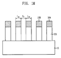
- FIGS. 1A to 1M illustrate cross-sectional views of a method for fabricating a fine pattern in a semiconductor device in accordance with an embodiment of the present invention.
- Embodiments of the present invention relate to a method for fabricating a fine pattern in a semiconductor device.
- FIGS. 1A to 1M illustrate cross-sectional views of a method for fabricating a fine pattern in a semiconductor device in accordance with an embodiment of the present invention.
- an etch target layer 12 e.g., a conductive layer or an insulation layer, is formed over a substrate 11 .
- a first bottom anti-reflective coating (BARC) layer 13 is formed over the etch target layer 12 .
- a first photoresist layer 14 is formed over the first BARC layer 13 .
- a photo mask process is performed using a photo-exposure and developing process to form a first photoresist pattern 14 A.
- a spacing distance between adjacent portions of the first photoresist pattern 14 A is referred to as a first spacing distance S P1 .
- the first BARC layer 13 is etched using the first photoresist pattern 14 A as an etch barrier.
- Reference numeral 13 A refers to an etched first BARC layer 13 A.
- a first hard mask layer 15 is formed over the first photoresist pattern 14 A and the etch target layer 12 .
- the first hard mask layer 15 includes a nitride-based layer, a silicon oxide layer, a tungsten layer, a polysilicon layer, or an amorphous carbon layer.
- the first hard mask layer 15 may be formed by performing a physical vapor deposition (PVD) method, a chemical vapor deposition (CVD) method, or a coating method.
- an etch-back process is performed to planarize the first hard mask layer 15 until the first photoresist pattern 14 A is exposed.
- a first hard mask pattern 15 A is formed.
- a portion of the first photoresist pattern 14 A may also be planarized while performing the etch-back process on the first hard mask layer 15 .
- a photoresist removal process is performed to remove the first photoresist pattern 14 A and the etched first BARC layer 13 A formed below the first photoresist pattern 14 A. Consequently, the first hard mask pattern 15 A remains over certain portions of the etch target layer 12 corresponding to the first spacing distance S P1 of the first photoresist pattern 14 A.
- a second BARC layer 16 is formed over the surface profile of the first hard mask pattern 15 A and the etch stop layer 12 .
- a second photoresist layer 17 is formed over the resultant structure, covering the first hard mask pattern 15 A.
- a photo mask process is performed using a photo-exposure and developing process to form a second photoresist pattern 17 A.
- a spacing distance between adjacent portions of the second photoresist pattern 17 A is referred to as a second spacing distance S P2 .
- the second photoresist pattern 17 A is formed in a structure that encloses the first hard mask pattern 15 A.
- the photo mask process for patterning the second photoresist layer 17 is performed in a manner that spacing distances and line widths of the first hard mask pattern 15 A and a subsequent second hard mask pattern are substantially the same.
- the second BARC layer 16 is etched using the second photoresist pattern 17 A as an etch barrier to expose certain portions of the etch target layer 12 .
- Reference numeral 16 A refers to an etched second BARC layer 16 A.
- a second hard mask layer 18 is formed over the second photoresist pattern 17 A and the etch target layer 12 .
- the second hard mask layer 18 includes a nitride-based layer, a silicon oxide layer, a tungsten layer, a polysilicon layer, or an amorphous carbon layer.
- the second hard mask layer 18 may be formed using a PVD method, a CVD method, or a coating method.
- an etch-back process is performed to planarize the second hard mask layer 18 such that an upper portion of the first hard mask pattern 15 A is exposed.
- a second hard mask pattern 18 A is formed.
- Reference numeral 15 B refers to a remaining first hard mask pattern 15 B.
- a portion of the second photoresist pattern 17 A may be planarized while performing the etch-back process on the second hard mask layer 18 .
- Reference numerals 17 B and 16 B refer to a remaining second photoresist pattern 17 B and a remaining second BARC layer 16 B, respectively.
- a photoresist removal process is performed to remove the remaining second photoresist pattern 17 B and the remaining second BARC layer 16 B.
- the second hard mask pattern 18 A corresponding to the second spacing distance S P2 of the second photoresist pattern 17 A is formed.
- the etch target layer 12 is etched to form an etch target pattern 12 A using the remaining first hard mask pattern 15 B and the second hard mask pattern 18 A as an etch barrier.
- the first and second line widths L H1 and L H2 of the remaining first hard mask pattern 15 B and the second hard mask pattern 18 A and a spacing distance S H between the remaining first hard mask pattern 15 B and the second hard mask pattern 18 A adjacent to each other are substantially the same.
- a line width of the etch target pattern 12 A which is substantially the same as the first and second line widths L H1 and L H2 , and the spacing distance S H between portions of the etch target pattern 12 A are substantially the same.
- two times of the photoresist patterning and the hard mask etch process are performed instead of using a multiple-layer hard mask structure as a hard mask for etching the etch target layer.
- the size change of the etch target pattern depending on the hard mask may be minimized.
- process cost may be reduced because the mask process is performed without using an expensive hard mask material.
- the embodiments of the present invention may be applied in most fields related to patterning in formation processes for semiconductor devices such as a dynamic random access memory (DRAM) or a flash.
- DRAM dynamic random access memory
- a change in the pattern size depending on the hard mask pattern may be minimized through repeatedly performing the mask patterning, the hard mask layer formation, and the etch process, instead of using a multiple-layer hard mask structure.
- the critical processes may be simplified, the fabrication cost may be decreased because expensive hard mask materials are generally not used.
Abstract
Description
Claims (6)
Applications Claiming Priority (2)
| Application Number | Priority Date | Filing Date | Title |
|---|---|---|---|
| KR2006-0095059 | 2006-09-28 | ||
| KR1020060095059A KR100798738B1 (en) | 2006-09-28 | 2006-09-28 | Method for fabricating fine pattern in semiconductor device |
Publications (2)
| Publication Number | Publication Date |
|---|---|
| US20080081479A1 US20080081479A1 (en) | 2008-04-03 |
| US7569477B2 true US7569477B2 (en) | 2009-08-04 |
Family
ID=39219533
Family Applications (1)
| Application Number | Title | Priority Date | Filing Date |
|---|---|---|---|
| US11/824,362 Expired - Fee Related US7569477B2 (en) | 2006-09-28 | 2007-06-29 | Method for fabricating fine pattern in semiconductor device |
Country Status (2)
| Country | Link |
|---|---|
| US (1) | US7569477B2 (en) |
| KR (1) | KR100798738B1 (en) |
Cited By (1)
| Publication number | Priority date | Publication date | Assignee | Title |
|---|---|---|---|---|
| US9012326B2 (en) | 2010-08-13 | 2015-04-21 | Samsung Electronics Co., Ltd. | Methods for patterning microelectronic devices using two sacrificial layers |
Families Citing this family (2)
| Publication number | Priority date | Publication date | Assignee | Title |
|---|---|---|---|---|
| KR101055962B1 (en) | 2008-05-15 | 2011-08-11 | 주성엔지니어링(주) | Thin film pattern formation method |
| KR102435855B1 (en) * | 2015-08-06 | 2022-08-25 | 삼성전자주식회사 | Method for forming hard mask patterns and method for manufacturing semiconductor device using the same |
Citations (11)
| Publication number | Priority date | Publication date | Assignee | Title |
|---|---|---|---|---|
| US5635423A (en) * | 1994-10-11 | 1997-06-03 | Advanced Micro Devices, Inc. | Simplified dual damascene process for multi-level metallization and interconnection structure |
| KR19990061090A (en) | 1997-12-31 | 1999-07-26 | 김영환 | Photoresist for multilayer resist process and fine pattern manufacturing method of semiconductor device using same |
| KR20010107233A (en) | 2000-05-26 | 2001-12-07 | 윤종용 | Semiconductor device fabricating method for use in minute pattern formation |
| US6833319B2 (en) * | 2001-12-19 | 2004-12-21 | Hynix Semiconductor Inc. | Method for fabricating semiconductor device |
| US20040266100A1 (en) * | 2003-06-25 | 2004-12-30 | Samsung Electronics Co., Ltd. | Method of fabricating semiconductor device having capacitor |
| US20050090055A1 (en) * | 2003-10-23 | 2005-04-28 | Min-Suk Lee | Method for fabricating semiconductor device with fine patterns |
| US20060094250A1 (en) * | 2004-09-30 | 2006-05-04 | Sung-Kwon Lee | Method for fabricating semiconductor device |
| US20070148983A1 (en) * | 2005-12-28 | 2007-06-28 | Hynix Semiconductor Inc. | Method for Manufacturing Semiconductor Device |
| US7309653B2 (en) * | 2005-02-24 | 2007-12-18 | International Business Machines Corporation | Method of forming damascene filament wires and the structure so formed |
| US7314810B2 (en) * | 2006-05-09 | 2008-01-01 | Hynix Semiconductor Inc. | Method for forming fine pattern of semiconductor device |
| US7479366B2 (en) * | 2003-11-06 | 2009-01-20 | Renesas Technology Corp. | Method for forming pattern |
-
2006
- 2006-09-28 KR KR1020060095059A patent/KR100798738B1/en not_active IP Right Cessation
-
2007
- 2007-06-29 US US11/824,362 patent/US7569477B2/en not_active Expired - Fee Related
Patent Citations (11)
| Publication number | Priority date | Publication date | Assignee | Title |
|---|---|---|---|---|
| US5635423A (en) * | 1994-10-11 | 1997-06-03 | Advanced Micro Devices, Inc. | Simplified dual damascene process for multi-level metallization and interconnection structure |
| KR19990061090A (en) | 1997-12-31 | 1999-07-26 | 김영환 | Photoresist for multilayer resist process and fine pattern manufacturing method of semiconductor device using same |
| KR20010107233A (en) | 2000-05-26 | 2001-12-07 | 윤종용 | Semiconductor device fabricating method for use in minute pattern formation |
| US6833319B2 (en) * | 2001-12-19 | 2004-12-21 | Hynix Semiconductor Inc. | Method for fabricating semiconductor device |
| US20040266100A1 (en) * | 2003-06-25 | 2004-12-30 | Samsung Electronics Co., Ltd. | Method of fabricating semiconductor device having capacitor |
| US20050090055A1 (en) * | 2003-10-23 | 2005-04-28 | Min-Suk Lee | Method for fabricating semiconductor device with fine patterns |
| US7479366B2 (en) * | 2003-11-06 | 2009-01-20 | Renesas Technology Corp. | Method for forming pattern |
| US20060094250A1 (en) * | 2004-09-30 | 2006-05-04 | Sung-Kwon Lee | Method for fabricating semiconductor device |
| US7309653B2 (en) * | 2005-02-24 | 2007-12-18 | International Business Machines Corporation | Method of forming damascene filament wires and the structure so formed |
| US20070148983A1 (en) * | 2005-12-28 | 2007-06-28 | Hynix Semiconductor Inc. | Method for Manufacturing Semiconductor Device |
| US7314810B2 (en) * | 2006-05-09 | 2008-01-01 | Hynix Semiconductor Inc. | Method for forming fine pattern of semiconductor device |
Cited By (1)
| Publication number | Priority date | Publication date | Assignee | Title |
|---|---|---|---|---|
| US9012326B2 (en) | 2010-08-13 | 2015-04-21 | Samsung Electronics Co., Ltd. | Methods for patterning microelectronic devices using two sacrificial layers |
Also Published As
| Publication number | Publication date |
|---|---|
| US20080081479A1 (en) | 2008-04-03 |
| KR100798738B1 (en) | 2008-01-29 |
Similar Documents
| Publication | Publication Date | Title |
|---|---|---|
| US8318603B2 (en) | Method of forming patterns for semiconductor device | |
| US7563712B2 (en) | Method of forming micro pattern in semiconductor device | |
| US7576010B2 (en) | Method of forming pattern using fine pitch hard mask | |
| US20090004862A1 (en) | Method for forming fine patterns in semiconductor device | |
| CN101772832A (en) | Semiconductor structures including tight pitch contacts and methods to form same | |
| US20120175745A1 (en) | Methods for fabricating semiconductor devices and semiconductor devices using the same | |
| US11769691B2 (en) | Semiconductor device and formation method thereof | |
| US20090117742A1 (en) | Method for fabricating fine pattern in semiconductor device | |
| US7981803B2 (en) | Method of forming micro pattern of semiconductor device | |
| US8053370B2 (en) | Semiconductor device and fabrications thereof | |
| CN112086433A (en) | Semiconductor element and method for manufacturing the same | |
| US10468252B2 (en) | Semiconductor device and method of manufacturing the same | |
| CN102522370A (en) | Formation method of contact hole | |
| US7569477B2 (en) | Method for fabricating fine pattern in semiconductor device | |
| KR20080022387A (en) | Method of fabricating bit line of semiconductor memory device | |
| CN114334619A (en) | Method for forming semiconductor structure | |
| US7553770B2 (en) | Reverse masking profile improvements in high aspect ratio etch | |
| US7977248B2 (en) | Double patterning with single hard mask | |
| US20080113515A1 (en) | Methods of Forming Semiconductor Devices | |
| US9230967B2 (en) | Method for forming self-aligned isolation trenches in semiconductor substrate and semiconductor device | |
| CN103050382A (en) | Manufacturing method of semiconductor device | |
| CN114823295A (en) | Method for manufacturing semiconductor device | |
| US20090162794A1 (en) | Method for fabricating semiconductor device | |
| US8114724B2 (en) | Method for fabricating semiconductor device | |
| KR100912959B1 (en) | Method for fabricating fine pattern in semiconductor device |
Legal Events
| Date | Code | Title | Description |
|---|---|---|---|
| AS | Assignment |
Owner name: HYNIX SEMICONDUCTOR INC., KOREA, REPUBLIC OF Free format text: ASSIGNMENT OF ASSIGNORS INTEREST;ASSIGNOR:PARK, JUNG-WOO;REEL/FRAME:019542/0412 Effective date: 20070626 |
|
| FEPP | Fee payment procedure |
Free format text: PAYOR NUMBER ASSIGNED (ORIGINAL EVENT CODE: ASPN); ENTITY STATUS OF PATENT OWNER: LARGE ENTITY |
|
| FPAY | Fee payment |
Year of fee payment: 4 |
|
| REMI | Maintenance fee reminder mailed | ||
| LAPS | Lapse for failure to pay maintenance fees |
Free format text: PATENT EXPIRED FOR FAILURE TO PAY MAINTENANCE FEES (ORIGINAL EVENT CODE: EXP.) |
|
| STCH | Information on status: patent discontinuation |
Free format text: PATENT EXPIRED DUE TO NONPAYMENT OF MAINTENANCE FEES UNDER 37 CFR 1.362 |
|
| FP | Lapsed due to failure to pay maintenance fee |
Effective date: 20170804 |