US7587809B2 - Method for forming a MR reader with reduced shield topography and low parasitic resistance - Google Patents
Method for forming a MR reader with reduced shield topography and low parasitic resistance Download PDFInfo
- Publication number
- US7587809B2 US7587809B2 US10/050,236 US5023602A US7587809B2 US 7587809 B2 US7587809 B2 US 7587809B2 US 5023602 A US5023602 A US 5023602A US 7587809 B2 US7587809 B2 US 7587809B2
- Authority
- US
- United States
- Prior art keywords
- magnetoresistive sensor
- stack
- sensor layers
- reader
- region
- Prior art date
- Legal status (The legal status is an assumption and is not a legal conclusion. Google has not performed a legal analysis and makes no representation as to the accuracy of the status listed.)
- Expired - Fee Related, expires
Links
Images


Classifications
-
- G—PHYSICS
- G11—INFORMATION STORAGE
- G11B—INFORMATION STORAGE BASED ON RELATIVE MOVEMENT BETWEEN RECORD CARRIER AND TRANSDUCER
- G11B5/00—Recording by magnetisation or demagnetisation of a record carrier; Reproducing by magnetic means; Record carriers therefor
- G11B5/127—Structure or manufacture of heads, e.g. inductive
- G11B5/33—Structure or manufacture of flux-sensitive heads, i.e. for reproduction only; Combination of such heads with means for recording or erasing only
- G11B5/39—Structure or manufacture of flux-sensitive heads, i.e. for reproduction only; Combination of such heads with means for recording or erasing only using magneto-resistive devices or effects
- G11B5/3903—Structure or manufacture of flux-sensitive heads, i.e. for reproduction only; Combination of such heads with means for recording or erasing only using magneto-resistive devices or effects using magnetic thin film layers or their effects, the films being part of integrated structures
- G11B5/398—Specially shaped layers
-
- G—PHYSICS
- G11—INFORMATION STORAGE
- G11B—INFORMATION STORAGE BASED ON RELATIVE MOVEMENT BETWEEN RECORD CARRIER AND TRANSDUCER
- G11B5/00—Recording by magnetisation or demagnetisation of a record carrier; Reproducing by magnetic means; Record carriers therefor
- G11B5/127—Structure or manufacture of heads, e.g. inductive
- G11B5/33—Structure or manufacture of flux-sensitive heads, i.e. for reproduction only; Combination of such heads with means for recording or erasing only
- G11B5/39—Structure or manufacture of flux-sensitive heads, i.e. for reproduction only; Combination of such heads with means for recording or erasing only using magneto-resistive devices or effects
- G11B5/3903—Structure or manufacture of flux-sensitive heads, i.e. for reproduction only; Combination of such heads with means for recording or erasing only using magneto-resistive devices or effects using magnetic thin film layers or their effects, the films being part of integrated structures
-
- H—ELECTRICITY
- H04—ELECTRIC COMMUNICATION TECHNIQUE
- H04R—LOUDSPEAKERS, MICROPHONES, GRAMOPHONE PICK-UPS OR LIKE ACOUSTIC ELECTROMECHANICAL TRANSDUCERS; DEAF-AID SETS; PUBLIC ADDRESS SYSTEMS
- H04R15/00—Magnetostrictive transducers
-
- G—PHYSICS
- G11—INFORMATION STORAGE
- G11B—INFORMATION STORAGE BASED ON RELATIVE MOVEMENT BETWEEN RECORD CARRIER AND TRANSDUCER
- G11B5/00—Recording by magnetisation or demagnetisation of a record carrier; Reproducing by magnetic means; Record carriers therefor
- G11B5/127—Structure or manufacture of heads, e.g. inductive
- G11B5/31—Structure or manufacture of heads, e.g. inductive using thin films
- G11B5/3109—Details
- G11B5/3116—Shaping of layers, poles or gaps for improving the form of the electrical signal transduced, e.g. for shielding, contour effect, equalizing, side flux fringing, cross talk reduction between heads or between heads and information tracks
-
- Y—GENERAL TAGGING OF NEW TECHNOLOGICAL DEVELOPMENTS; GENERAL TAGGING OF CROSS-SECTIONAL TECHNOLOGIES SPANNING OVER SEVERAL SECTIONS OF THE IPC; TECHNICAL SUBJECTS COVERED BY FORMER USPC CROSS-REFERENCE ART COLLECTIONS [XRACs] AND DIGESTS
- Y10—TECHNICAL SUBJECTS COVERED BY FORMER USPC
- Y10T—TECHNICAL SUBJECTS COVERED BY FORMER US CLASSIFICATION
- Y10T29/00—Metal working
- Y10T29/49—Method of mechanical manufacture
- Y10T29/49002—Electrical device making
- Y10T29/4902—Electromagnet, transformer or inductor
- Y10T29/49021—Magnetic recording reproducing transducer [e.g., tape head, core, etc.]
- Y10T29/49032—Fabricating head structure or component thereof
- Y10T29/49036—Fabricating head structure or component thereof including measuring or testing
- Y10T29/49041—Fabricating head structure or component thereof including measuring or testing with significant slider/housing shaping or treating
-
- Y—GENERAL TAGGING OF NEW TECHNOLOGICAL DEVELOPMENTS; GENERAL TAGGING OF CROSS-SECTIONAL TECHNOLOGIES SPANNING OVER SEVERAL SECTIONS OF THE IPC; TECHNICAL SUBJECTS COVERED BY FORMER USPC CROSS-REFERENCE ART COLLECTIONS [XRACs] AND DIGESTS
- Y10—TECHNICAL SUBJECTS COVERED BY FORMER USPC
- Y10T—TECHNICAL SUBJECTS COVERED BY FORMER US CLASSIFICATION
- Y10T29/00—Metal working
- Y10T29/49—Method of mechanical manufacture
- Y10T29/49002—Electrical device making
- Y10T29/4902—Electromagnet, transformer or inductor
- Y10T29/49021—Magnetic recording reproducing transducer [e.g., tape head, core, etc.]
- Y10T29/49032—Fabricating head structure or component thereof
- Y10T29/49036—Fabricating head structure or component thereof including measuring or testing
- Y10T29/49043—Depositing magnetic layer or coating
- Y10T29/49044—Plural magnetic deposition layers
-
- Y—GENERAL TAGGING OF NEW TECHNOLOGICAL DEVELOPMENTS; GENERAL TAGGING OF CROSS-SECTIONAL TECHNOLOGIES SPANNING OVER SEVERAL SECTIONS OF THE IPC; TECHNICAL SUBJECTS COVERED BY FORMER USPC CROSS-REFERENCE ART COLLECTIONS [XRACs] AND DIGESTS
- Y10—TECHNICAL SUBJECTS COVERED BY FORMER USPC
- Y10T—TECHNICAL SUBJECTS COVERED BY FORMER US CLASSIFICATION
- Y10T29/00—Metal working
- Y10T29/49—Method of mechanical manufacture
- Y10T29/49002—Electrical device making
- Y10T29/4902—Electromagnet, transformer or inductor
- Y10T29/49021—Magnetic recording reproducing transducer [e.g., tape head, core, etc.]
- Y10T29/49032—Fabricating head structure or component thereof
- Y10T29/49036—Fabricating head structure or component thereof including measuring or testing
- Y10T29/49043—Depositing magnetic layer or coating
- Y10T29/49046—Depositing magnetic layer or coating with etching or machining of magnetic material
-
- Y—GENERAL TAGGING OF NEW TECHNOLOGICAL DEVELOPMENTS; GENERAL TAGGING OF CROSS-SECTIONAL TECHNOLOGIES SPANNING OVER SEVERAL SECTIONS OF THE IPC; TECHNICAL SUBJECTS COVERED BY FORMER USPC CROSS-REFERENCE ART COLLECTIONS [XRACs] AND DIGESTS
- Y10—TECHNICAL SUBJECTS COVERED BY FORMER USPC
- Y10T—TECHNICAL SUBJECTS COVERED BY FORMER US CLASSIFICATION
- Y10T29/00—Metal working
- Y10T29/49—Method of mechanical manufacture
- Y10T29/49002—Electrical device making
- Y10T29/4902—Electromagnet, transformer or inductor
- Y10T29/49021—Magnetic recording reproducing transducer [e.g., tape head, core, etc.]
- Y10T29/49032—Fabricating head structure or component thereof
- Y10T29/49048—Machining magnetic material [e.g., grinding, etching, polishing]
- Y10T29/49052—Machining magnetic material [e.g., grinding, etching, polishing] by etching
Definitions
- the present invention relates to manufacturing of magnetoresistive spin valve (SV) devices.
- the present invention relates to a method of fabricating abutted junction SV heads for longitudinal recording.
- a magnetic read head retrieves magnetically-encoded information that is stored on a magnetic medium or disc.
- the magnetic read head is typically formed of several layers that include a top shield, a bottom shield, and a read sensor positioned between the top and bottom shields. Also positioned between the top and bottom shields, abutting opposite sides of the read sensor, are biasing layers and current contacts.
- the read sensor is generally a type of magnetoresistive (MR) sensor.
- the resistance of the MR sensor fluctuates in response to a magnetic field emanating from a magnetic medium when the MR sensor is used in a magnetic read head and positioned near the magnetic medium. By providing a sense current through the MR sensor, the resistance of the MR sensor can be measured and used by external circuitry to decipher the information stored on the magnetic medium.
- the spin valve effect is one known way to utilize magnetoresistance.
- Present abutted junction SV technology utilizes SV stacks with a thickness around 400 angstroms, while a combined thickness of surrounding biasing layers and current contacts is close to 1000 angstroms. This 600 angstrom difference in thickness creates a non-planar top shield topography near the sensor. For SV readers targeted at 100 kTPI and above, this top shield non-planar topography is comparable to the lateral dimensions of the reader. As a result, this non-planar topography presents serious concerns.
- the top shield is made of soft magnetic material, which tends to break into magnetic domains in regions with corners and non-planar topography. Formation of magnetic domains in the top shield that are in close vicinity to the MR sensor is highly undesirable, because it is expected to be a source of magnetic instability and, thus, increase noise in the reader.
- the top and bottom shields need to shield the MR sensor from down-track transitions on the magnetic media and enable adequate electrical pulse-width (PW 50 ), which is the width of the pulse signal at 50% peak amplitude, of the MR read sensor. These are achieved when a spacing between the bottom shield and the top shield are at a minimum. Large top shield non-planar topography is expected to compromise the shield-to-shield spacing at the edges of the sensor, thus deteriorating the down-track shielding capability and the PW 50 .
- PW 50 electrical pulse-width
- top and bottom shields need to shield the MR sensor from transitions in adjacent tracks on the magnetic media and provide adequate electrical reader width, which is evaluated by the MT 50 and MT 10 values.
- MT 50 and MT 10 values are the width of the pulse signal at 50% and 10% peak amplitude, respectively. Large top shield non-planar topography is expected to allow more flux penetration from the adjacent tracks. This will lead to deteriorated MT 50 /MT 10 values or, alternatively, would require narrower physical reader width to achieve the required electrical reader width.
- the conventional method of fabricating MR readers first defines a reader width of the MR sensor and then defines a back edge of a stripe height of the MR sensor. As will be explained below, this process creates a region of significantly thinned current contacts behind the stripe height back edge. After lapping an air bearing surface (ABS) of the MR sensor to define a stripe height front edge, the thickness of the remaining part of the current contacts is significantly reduced. Consequently, current supplied to the MR sensor through the current contacts is forced to go through two paths that have high resistance—one is a thick but narrow strip at the ABS, while the other is a wide but thin region extending behind the stripe height back edge. This creates large parasitic resistance.
- ABS air bearing surface
- the present invention is a method for fabricating a magnetoresistive reader having a sensor, current contacts with low parasitic resistance and a top shield with substantially planar topology.
- a stripe height back edge of the sensor is defined, and second, a reader width of the sensor is defined.
- the current contacts are deposited to a thickness such that a top surface of the current contacts is substantially level with a top surface of the sensor.
- the top shield is deposited over the sensor and the current contacts. Defining the stripe height back edge prior to the reader width results in current contacts with low parasitic resistance and allows for thin contacts and flat top shield, which inhibits the formation of magnetic domains in the top shield.
- FIGS. 1-5 illustrate steps in a conventional method for forming a MR reader.
- FIGS. 6-9 illustrate steps in accord with the present invention for forming a MR reader.
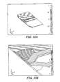
- FIGS. 10 a and 10 b are electrical potential distribution maps of a MR reader made by the conventional method.
- FIGS. 11 a and 11 b are electrical potential distribution maps of a MR reader made by the method of the present invention.
- FIG. 12 is a graphical representation comparing a parasitic resistance contribution from the fabrication process (Rmill) to a mill window width (MW) used to fabricate MR readers.
- FIG. 13 is a graphical representation comparing Rmill to a stripe height of MR readers.
- a sensor of an MR reader is formed by defining four critical edges: a front and back edge defining a stripe height of the sensor and side edges defining a width of the sensor (a reader width).
- the reader width is defined first, followed by definition of the stripe height back edge and then the stripe height front edge.
- FIGS. 1-5 illustrate steps in a conventional method of forming MR reader 10 .
- FIG. 1 is a cross-sectional view of MR reader 10 in the process of having its reader width defined by the conventional method.
- MR reader 10 includes bottom shield 12 , bottom half-gap 14 , SV stack 16 having reader width 18 , photoresist release layer (PMGI) or photoresist bridge 19 , and photoresist layer 20 .
- Bottom shield 12 is deposited on a wafer (not shown) covered with an appropriate basecoat (Al 2 O 3 layer) followed by bottom half-gap 14 and then SV stack 16 .
- Bottom half-gap 14 is an insulator that is usually made of Al 2 O 3 .
- a specific pattern of photoresist layer 20 is suspended over SV stack 16 using photoresist release layer (PMGI) or photoresist bridge 19 .
- a width of photoresist layer 20 adjacent to a desired SV sensor region of SV stack 16 defines reader width 18 of SV stack 16 .
- photoresist layer 20 The purpose of photoresist layer 20 is to mask regions during the milling process, which removes the material left unprotected.
- MR reader 10 with reader width 18 defined after the milling process is shown in FIG. 1 . At this point, two of the critical edges are defined: the side edges of reader width 18 of SV stack 16 .
- FIG. 2 is a cross-sectional view of MR reader 10 illustrating another step in the conventional method of fabricating MR reader 10 .
- This step involves depositing several layers in an abutting junction configuration adjacent opposite edges of SV stack 16 .
- the specific components may vary, for example a pedestal may be included.
- permanent magnet seed 22 is deposited, then permanent magnet 24 , followed by extended contacts 26 .
- photoresist layer 20 is dissolved (not shown).
- FIG. 3 is a top view of MR reader 10 showing MR reader 10 masked for defining stripe height back edge 30 .
- Photoresist layer 28 masks part of SV stack 16 and contacts 26 but leaves open the area behind desired stripe height back edge 30 , which is defined.
- Stripe height back edge 30 is protected by backfilling the milled area with Al 2 O 3 or other suitable material, and photoresist layer 28 is subsequently dissolved.
- the last step involves defining the final critical edge, which is the front edge of the stripe height. Lapping MR reader 10 at the front edge defines the stripe height front edge (or the ABS).
- FIG. 4 is a top view of MR reader 10 schematically showing MR reader 10 with defined sensor 32 .
- sensor 32 After lapping the ABS of MR reader 10 , sensor 32 is fully defined having reader width 18 and stripe height 36 .
- the second milling process has cleared the exposed SV stack 16 and contacts 26 .
- Bottom half-gap 14 is exposed from underneath SV stack 16 .
- Exposed contacts 26 have been milled to a very minimal thickness represented by milled contacts 38 .
- Contacts 26 now form a thick but narrow region near sensor 32 . This configuration leads to large parasitic resistance as current is directed toward sensor 32 .
- the current is forced through contact paths that are thick but narrow (contacts 26 ) and wide but thin (milled contacts 38 ).
- FIG. 5 is a cross-sectional view of finished SV reader 10 .
- top half-gap 40 has been deposited over contacts 26 , milled contacts 38 (not shown), and SV stack 16 .
- Top shield 42 is then deposited over top half-gap 40 .
- top shield 42 also has non-planar topography. As previously discussed, this leads to magnetic domains forming in top shield 42 that may interfere with the signal generated by SV reader 10 .
- top shield 42 non-planar topography is to use two sets of contacts: a first set that matches SV stack 16 thickness and extends out from sensor 32 , and a second set that is much thicker and recessed from sensor 32 . With this approach, the non-planar topography of top shield 42 is moved away from sensor 32 .
- FIGS. 6-9 alleviates the problems associated with the previously described conventional techniques.
- the process begins, as with the conventional method, by depositing bottom shield 12 , bottom half-gap 14 , and SV stack 16 .
- FIG. 6 which is a top view of MR reader 50 , illustrates the step of defining stripe height back edge 30 .
- FIG. 6 shows photoresist layer 28 selectively patterned on SV stack 16 , leaving exposed a region of SV stack 16 behind desired stripe height back edge 30 to define stripe height back edge 30 .
- MR reader 50 is milled and bottom half-gap 14 is revealed in the unprotected region.
- the first critical edge, stripe height back edge 30 is defined.
- Stripe height back edge 30 is backfilled to protect edge 30 and photoresist layer 28 is subsequently dissolved.
- the backfill is Al 3 O 2 , and has a thickness that leaves enough insulation after the milling process to define reader width 18 .
- the backfill should be at about the same level as SV stack 16 .
- FIG. 7 shows the next step in the process, which is defining reader width 18 .
- FIG. 7 shows MR reader 50 with photoresist layer 20 ; bottom half-gap 14 , which was exposed in the previous mill process; and SV stack 16 with stripe height back edge 30 , which was masked in the previous step.
- photoresist layer 20 serves to define reader width 18 of MR reader 50 .
- MR reader 50 is milled again to remove an unprotected region of SV stack 16 .
- Photoresist layer 20 remains while contacts 26 are deposited such that a top surface of SV stack 16 extends at a same level as a top surface of contacts 26 .
- other materials are deposited prior to contacts 26 . These materials may include a pedestal layer, permanent magnet seed, and permanent magnet.
- Photoresist layer 20 is subsequently dissolved. Reader width 18 is now defined.
- top half-gap 40 is deposited and then top shield 42 is deposited.
- Stripe height front edge 34 is defined, as in the conventional method, by lapping the ABS of MR reader 50 to finalize definition of all critical edges of sensor 32 .
- FIGS. 8 and 9 show finished MR reader 50 .
- FIG. 8 is a top view without top gap 40 or top shield 42
- FIG. 9 is a cross-sectional, ABS view of finished SV reader 50 .
- SV reader 50 includes bottom shield 12 , bottom gap 14 , sensor 32 having reader width 18 and stripe height 36 defined by back and front edges 30 and 34 , respectively; permanent magnet seed 22 ; permanent magnets 24 ; current contacts 26 ; top gap 40 ; and top shield 42 .
- contacts 26 have uniform thickness throughout.
- the wide layer forming contacts 26 has reasonably large (about 400 angstroms) thickness and decreased parasitic resistance to acceptable levels.
- top shield 42 exhibits planar topography since contacts 26 and SV stack 16 have planar topography. The problem of magnetic domains forming and interfering with sensor 32 is reduced because of this planar topography of top shield 42 .
- only one set of contacts 26 are used, which decreases process time, cost, and scrapped wafers.
- Finite element method (FEM) modeling was performed to study the parasitic resistance contribution from the milling process that defines stripe height 36 (Rmill).
- a SV reader fabricated using the conventional method was compared to a SV reader fabricated using the method of the present invention.
- a top surface of contacts 26 was assumed to be substantially level with a top surface of SV stack 16 , which is 400 angstroms.
- a width of a mill window in photoresist layer 28 (MW), which defines stripe height back edge 30 is a major factor in determining Rmill in the conventional method. Therefore, three different widths were tested: 0.55 ⁇ m, 0.75 ⁇ m, and 1.0 ⁇ m.
- MW can not be reduced to an arbitrarily low value because of limitations in achieving a straight stripe height back edge 30 .
- the minimum width is 0.55 ⁇ m.
- Current 30 Gb/inch 2 to 50 Gb/inch 2 products use a 1.0 ⁇ m width.
- the examples studied all utilized Rhodium (Rh) or Gold (Au) pedestals, but the pedestals may be formed of other conductive material. Additionally, the SV reader can be formed without pedestals as illustrated above in FIGS. 6-9 .
- FIGS. 10 a and 10 b show the electrical potential distribution map of a SV reader fabricated using the conventional method with a Rh pedestal and MW of 0.55 ⁇ m.
- FIG. 10 b is an enlarged view of active sensor 32 illustrated in FIG. 10 a . Since contacts 26 are thinned by the milling process, current is squeezed through a narrow strip at the ABS causing a large parasitic resistance.
- FIGS. 11 a and 11 b are analogous electrical potential distributions of a SV reader fabricated using the method of the present invention.
- FIG. 11 b is an enlarged view of active sensor 32 illustrated in FIG. 11 a .
- the current is not constrained so drastically, and this insures much lower Rmill.
- MW is irrelevant in this case, thus allowing MW to be optimized using other process constraints such as straightness of stripe height back edge 30 , shadowing during milling, stripe height back edge 30 backfill process, and photoresist liftoffs.
- Rmill was calculated for a number of cases. The results are presented in FIG. 12 .
- Stripe height 36 is assumed to be 400 angstroms, which is close to the target value for programs between 120-140 kTPI.
- the minimum Rmill is 107 ⁇ and with an Au pedestal, the minimum Rmill is 70 ⁇ . Even the smaller 70 ⁇ value is much larger than the values of Rmill presently used, which are about 20-30 ⁇ and will render head resistances of 115 ⁇ for Au and 150 ⁇ for Rh pedestals.
- the Rmill is 38 ⁇ . If an Au pedestal is used, the Rmill is 25 ⁇ which is well within the range used in present technology.
- FIG. 13 shows the results of comparing Rmill as a function of stripe height 36 .
- the pedestals are formed of Rh and MW is 0.75 ⁇ m.
- Using the conventional method to form the SV reader results in a strong inverse correspondence between Rmill and stripe height 36 .
- the lapping processes produce significant variations in stripe height 36 .
- the large variation in head resistance, as well as the large value itself, is not optimal for the design of the associated electronics.
- Rmill has little dependence on stripe height 36 .
- typical variations in stripe height 36 do not substantially change the geometry of contacts 26 .
- the current still passes through the same wide region and, thus, the small stripe height 36 dependence.
- the resulting area that the current passes through is a narrow, long strip along the ABS, and the typical variations in stripe height 36 will strongly affect resistance.
- CIP current in plane
Abstract
Description
Claims (24)
Priority Applications (1)
| Application Number | Priority Date | Filing Date | Title |
|---|---|---|---|
| US10/050,236 US7587809B2 (en) | 2001-09-12 | 2002-01-15 | Method for forming a MR reader with reduced shield topography and low parasitic resistance |
Applications Claiming Priority (2)
| Application Number | Priority Date | Filing Date | Title |
|---|---|---|---|
| US32231101P | 2001-09-12 | 2001-09-12 | |
| US10/050,236 US7587809B2 (en) | 2001-09-12 | 2002-01-15 | Method for forming a MR reader with reduced shield topography and low parasitic resistance |
Publications (2)
| Publication Number | Publication Date |
|---|---|
| US20030046807A1 US20030046807A1 (en) | 2003-03-13 |
| US7587809B2 true US7587809B2 (en) | 2009-09-15 |
Family
ID=26728046
Family Applications (1)
| Application Number | Title | Priority Date | Filing Date |
|---|---|---|---|
| US10/050,236 Expired - Fee Related US7587809B2 (en) | 2001-09-12 | 2002-01-15 | Method for forming a MR reader with reduced shield topography and low parasitic resistance |
Country Status (1)
| Country | Link |
|---|---|
| US (1) | US7587809B2 (en) |
Cited By (5)
| Publication number | Priority date | Publication date | Assignee | Title |
|---|---|---|---|---|
| US20070268631A1 (en) * | 2004-02-03 | 2007-11-22 | Headway Technologies, Inc. | Method to achieve both narrow track width and effective longitudinal stabilization in a CPP GMR read head |
| US8922954B2 (en) | 2013-05-06 | 2014-12-30 | Seagate Technology Llc | Data reader with back edge surface |
| US8922952B2 (en) | 2013-03-15 | 2014-12-30 | Seagate Technology Llc | Shaped data sensor shield contacts |
| US9387568B1 (en) * | 2013-02-27 | 2016-07-12 | Western Digital Technologies, Inc. | Systems and methods for correcting fabrication error in magnetic recording heads using magnetic write width measurements |
| US10224066B1 (en) | 2017-11-28 | 2019-03-05 | Seagate Technology Llc | Electrical isolation of read sensors during fabrication |
Families Citing this family (2)
| Publication number | Priority date | Publication date | Assignee | Title |
|---|---|---|---|---|
| US7211339B1 (en) * | 2002-08-22 | 2007-05-01 | Western Digital (Fremont), Inc. | Highly conductive lead adjoining MR stripe and extending beyond stripe height at junction |
| US20080088985A1 (en) * | 2006-10-16 | 2008-04-17 | Driskill-Smith Alexander Adria | Magnetic head having CPP sensor with partially milled stripe height |
Citations (12)
| Publication number | Priority date | Publication date | Assignee | Title |
|---|---|---|---|---|
| US5668688A (en) | 1996-05-24 | 1997-09-16 | Quantum Peripherals Colorado, Inc. | Current perpendicular-to-the-plane spin valve type magnetoresistive transducer |
| US5722157A (en) * | 1995-06-28 | 1998-03-03 | Yamaha Corporation | Method of making an induction and magnetoresistance type composite magnetic head |
| US5847904A (en) * | 1995-12-08 | 1998-12-08 | Quantum Peripherals Colorado, Inc. | Magnetoresistive device incorporating conductor geometry providing substantially uniform current flow for improved magnetic stability |
| US5946167A (en) | 1996-03-15 | 1999-08-31 | Kabushiki Kaisha Toshiba | Magnetoresistive sensor having lead and/or bias layer structure contributing to a narrow gap |
| US6032353A (en) * | 1997-05-15 | 2000-03-07 | Read-Rite Corporation | Magnetic head with low stack height and self-aligned pole tips |
| JP2000076630A (en) * | 1998-09-01 | 2000-03-14 | Read Rite Smi Kk | Manufacture of magnetoresistive type magnetic head and thin film magnetic head |
| US6055136A (en) * | 1995-09-11 | 2000-04-25 | International Business Machines Corporation | Spin valve sensor with antiparallel magnetization of pinned layers |
| US6085406A (en) * | 1998-10-21 | 2000-07-11 | International Business Machines Corporation | Method of making a read head with improved lead layers at an air bearing surface |
| US6230389B1 (en) | 1998-11-19 | 2001-05-15 | Headway Technologies, Inc. | Method for fabricating a magnetoresistive (MR) stripe height lapping monitor with improved linearity |
| US6262869B1 (en) * | 1999-08-02 | 2001-07-17 | International Business Machines Corporation | Spin valve sensor with encapsulated keeper layer and method of making |
| US20020067579A1 (en) | 1997-12-09 | 2002-06-06 | Kiyoshi Sato | Thin magnetic head with intermediate gap layer, magnetoresistive layer and electrode layers disposed between upper and lower gap layers |
| US6609948B1 (en) * | 2000-11-27 | 2003-08-26 | International Business Machines Corporation | Method of making an electronic lapping guide (ELG) for lapping a read sensor |
-
2002
- 2002-01-15 US US10/050,236 patent/US7587809B2/en not_active Expired - Fee Related
Patent Citations (12)
| Publication number | Priority date | Publication date | Assignee | Title |
|---|---|---|---|---|
| US5722157A (en) * | 1995-06-28 | 1998-03-03 | Yamaha Corporation | Method of making an induction and magnetoresistance type composite magnetic head |
| US6055136A (en) * | 1995-09-11 | 2000-04-25 | International Business Machines Corporation | Spin valve sensor with antiparallel magnetization of pinned layers |
| US5847904A (en) * | 1995-12-08 | 1998-12-08 | Quantum Peripherals Colorado, Inc. | Magnetoresistive device incorporating conductor geometry providing substantially uniform current flow for improved magnetic stability |
| US5946167A (en) | 1996-03-15 | 1999-08-31 | Kabushiki Kaisha Toshiba | Magnetoresistive sensor having lead and/or bias layer structure contributing to a narrow gap |
| US5668688A (en) | 1996-05-24 | 1997-09-16 | Quantum Peripherals Colorado, Inc. | Current perpendicular-to-the-plane spin valve type magnetoresistive transducer |
| US6032353A (en) * | 1997-05-15 | 2000-03-07 | Read-Rite Corporation | Magnetic head with low stack height and self-aligned pole tips |
| US20020067579A1 (en) | 1997-12-09 | 2002-06-06 | Kiyoshi Sato | Thin magnetic head with intermediate gap layer, magnetoresistive layer and electrode layers disposed between upper and lower gap layers |
| JP2000076630A (en) * | 1998-09-01 | 2000-03-14 | Read Rite Smi Kk | Manufacture of magnetoresistive type magnetic head and thin film magnetic head |
| US6085406A (en) * | 1998-10-21 | 2000-07-11 | International Business Machines Corporation | Method of making a read head with improved lead layers at an air bearing surface |
| US6230389B1 (en) | 1998-11-19 | 2001-05-15 | Headway Technologies, Inc. | Method for fabricating a magnetoresistive (MR) stripe height lapping monitor with improved linearity |
| US6262869B1 (en) * | 1999-08-02 | 2001-07-17 | International Business Machines Corporation | Spin valve sensor with encapsulated keeper layer and method of making |
| US6609948B1 (en) * | 2000-11-27 | 2003-08-26 | International Business Machines Corporation | Method of making an electronic lapping guide (ELG) for lapping a read sensor |
Cited By (6)
| Publication number | Priority date | Publication date | Assignee | Title |
|---|---|---|---|---|
| US20070268631A1 (en) * | 2004-02-03 | 2007-11-22 | Headway Technologies, Inc. | Method to achieve both narrow track width and effective longitudinal stabilization in a CPP GMR read head |
| US8059372B2 (en) * | 2004-02-03 | 2011-11-15 | Headway Technologies, Inc. | CPP GMR read head with minimum shunting loss |
| US9387568B1 (en) * | 2013-02-27 | 2016-07-12 | Western Digital Technologies, Inc. | Systems and methods for correcting fabrication error in magnetic recording heads using magnetic write width measurements |
| US8922952B2 (en) | 2013-03-15 | 2014-12-30 | Seagate Technology Llc | Shaped data sensor shield contacts |
| US8922954B2 (en) | 2013-05-06 | 2014-12-30 | Seagate Technology Llc | Data reader with back edge surface |
| US10224066B1 (en) | 2017-11-28 | 2019-03-05 | Seagate Technology Llc | Electrical isolation of read sensors during fabrication |
Also Published As
| Publication number | Publication date |
|---|---|
| US20030046807A1 (en) | 2003-03-13 |
Similar Documents
| Publication | Publication Date | Title |
|---|---|---|
| US6195229B1 (en) | Thin film MR head and method of making wherein pole trim takes place at the wafer level | |
| US7036208B2 (en) | Self aligned magnetoresistive flux guide read head with exchange bias underneath free layer | |
| KR100243822B1 (en) | Magnetoresistive sensor and the method of preparing a magnetoresistive sensor | |
| US8335056B2 (en) | CPP sensors with hard bias structures that shunt sense current towards a shield | |
| US5774308A (en) | Thin film inductive head and magnetic writing/reading drive including the same | |
| US6563678B2 (en) | Thin-film magnetic head having insolating layer provided between gap layer and shielding layer | |
| US5867889A (en) | Double self-aligned insulated contiguous junction for flux-guided-MR or yoke-MR head applications | |
| JP2001344716A (en) | Method for manufacturing magnetoresistive head | |
| JP3708827B2 (en) | Thin film magnetic head and manufacturing method thereof | |
| US7587809B2 (en) | Method for forming a MR reader with reduced shield topography and low parasitic resistance | |
| US7158352B2 (en) | Magnetoresistive device and method of manufacturing same, and thin-film magnetic head and method of manufacturing same | |
| US6301085B1 (en) | Thin film magnetic head | |
| US6901651B2 (en) | Method of manufacturing thin-film magnetic head | |
| US6477765B1 (en) | Method of fabricating a magnetic write transducer | |
| JP2002216321A (en) | Thin film magnetic head, its manufacturing method, and thin film pattern forming method for thin film magnetic head | |
| KR20080029727A (en) | Magnetic head and method of producing the same | |
| US6842314B2 (en) | Magnetoresistive device and method of manufacturing same, and thin-film magnetic head and method of manufacturing same | |
| JP2004171692A (en) | Combination type magnetic head | |
| US7107667B2 (en) | Method for fabricating thin film magnetic head | |
| JP2000293816A (en) | Thin film magnetic head and its production | |
| US7768748B2 (en) | Magnetoresistive sensor with overlaid combined leads and shields | |
| US6700740B2 (en) | Thin-film magnetic head and method of manufacturing same | |
| US7500303B2 (en) | Method of fabricating a magnetic sensor on a wafer | |
| US20030067718A1 (en) | Slider of thin-film magnetic head and method of manufacturing same | |
| JP2002353538A (en) | Magnetic detecting element, manufacturing method therefor, and magnetic head |
Legal Events
| Date | Code | Title | Description |
|---|---|---|---|
| AS | Assignment |
Owner name: SEAGATE TECHNOLOGY LLC, CALIFORNIA Free format text: ASSIGNMENT OF ASSIGNORS INTEREST;ASSIGNORS:DIMITROV, DIMITAR V.;BURBANK, DANIEL P.;ANDERSON, PAUL E.;AND OTHERS;REEL/FRAME:012509/0719;SIGNING DATES FROM 20020102 TO 20020107 |
|
| AS | Assignment |
Owner name: JPMORGAN CHASE BANK, AS COLLATERAL AGENT, NEW YORK Free format text: SECURITY AGREEMENT;ASSIGNOR:SEAGATE TECHNOLOGY LLC;REEL/FRAME:013177/0001 Effective date: 20020513 Owner name: JPMORGAN CHASE BANK, AS COLLATERAL AGENT,NEW YORK Free format text: SECURITY AGREEMENT;ASSIGNOR:SEAGATE TECHNOLOGY LLC;REEL/FRAME:013177/0001 Effective date: 20020513 |
|
| AS | Assignment |
Owner name: SEAGATE TECHNOLOGY LLC,CALIFORNIA Free format text: RELEASE OF SECURITY INTERESTS IN PATENT RIGHTS;ASSIGNOR:JPMORGAN CHASE BANK, N.A., AS ADMINISTRATIVE AGENT (FORMERLY KNOWN AS THE CHASE MANHATTAN BANK AND JPMORGAN CHASE BANK);REEL/FRAME:016926/0342 Effective date: 20051130 Owner name: SEAGATE TECHNOLOGY LLC, CALIFORNIA Free format text: RELEASE OF SECURITY INTERESTS IN PATENT RIGHTS;ASSIGNOR:JPMORGAN CHASE BANK, N.A., AS ADMINISTRATIVE AGENT (FORMERLY KNOWN AS THE CHASE MANHATTAN BANK AND JPMORGAN CHASE BANK);REEL/FRAME:016926/0342 Effective date: 20051130 |
|
| AS | Assignment |
Owner name: JPMORGAN CHASE BANK, N.A., AS ADMINISTRATIVE AGENT Free format text: SECURITY AGREEMENT;ASSIGNORS:MAXTOR CORPORATION;SEAGATE TECHNOLOGY LLC;SEAGATE TECHNOLOGY INTERNATIONAL;REEL/FRAME:022757/0017 Effective date: 20090507 Owner name: WELLS FARGO BANK, NATIONAL ASSOCIATION, AS COLLATE Free format text: SECURITY AGREEMENT;ASSIGNORS:MAXTOR CORPORATION;SEAGATE TECHNOLOGY LLC;SEAGATE TECHNOLOGY INTERNATIONAL;REEL/FRAME:022757/0017 Effective date: 20090507 |
|
| STCF | Information on status: patent grant |
Free format text: PATENTED CASE |
|
| CC | Certificate of correction | ||
| AS | Assignment |
Owner name: SEAGATE TECHNOLOGY HDD HOLDINGS, CALIFORNIA Free format text: RELEASE;ASSIGNOR:JPMORGAN CHASE BANK, N.A., AS ADMINISTRATIVE AGENT;REEL/FRAME:025662/0001 Effective date: 20110114 Owner name: MAXTOR CORPORATION, CALIFORNIA Free format text: RELEASE;ASSIGNOR:JPMORGAN CHASE BANK, N.A., AS ADMINISTRATIVE AGENT;REEL/FRAME:025662/0001 Effective date: 20110114 Owner name: SEAGATE TECHNOLOGY INTERNATIONAL, CALIFORNIA Free format text: RELEASE;ASSIGNOR:JPMORGAN CHASE BANK, N.A., AS ADMINISTRATIVE AGENT;REEL/FRAME:025662/0001 Effective date: 20110114 Owner name: SEAGATE TECHNOLOGY LLC, CALIFORNIA Free format text: RELEASE;ASSIGNOR:JPMORGAN CHASE BANK, N.A., AS ADMINISTRATIVE AGENT;REEL/FRAME:025662/0001 Effective date: 20110114 |
|
| AS | Assignment |
Owner name: THE BANK OF NOVA SCOTIA, AS ADMINISTRATIVE AGENT, Free format text: SECURITY AGREEMENT;ASSIGNOR:SEAGATE TECHNOLOGY LLC;REEL/FRAME:026010/0350 Effective date: 20110118 |
|
| FPAY | Fee payment |
Year of fee payment: 4 |
|
| AS | Assignment |
Owner name: SEAGATE TECHNOLOGY LLC, CALIFORNIA Free format text: TERMINATION AND RELEASE OF SECURITY INTEREST IN PATENT RIGHTS;ASSIGNOR:WELLS FARGO BANK, NATIONAL ASSOCIATION, AS COLLATERAL AGENT AND SECOND PRIORITY REPRESENTATIVE;REEL/FRAME:030833/0001 Effective date: 20130312 Owner name: EVAULT INC. (F/K/A I365 INC.), CALIFORNIA Free format text: TERMINATION AND RELEASE OF SECURITY INTEREST IN PATENT RIGHTS;ASSIGNOR:WELLS FARGO BANK, NATIONAL ASSOCIATION, AS COLLATERAL AGENT AND SECOND PRIORITY REPRESENTATIVE;REEL/FRAME:030833/0001 Effective date: 20130312 Owner name: SEAGATE TECHNOLOGY INTERNATIONAL, CAYMAN ISLANDS Free format text: TERMINATION AND RELEASE OF SECURITY INTEREST IN PATENT RIGHTS;ASSIGNOR:WELLS FARGO BANK, NATIONAL ASSOCIATION, AS COLLATERAL AGENT AND SECOND PRIORITY REPRESENTATIVE;REEL/FRAME:030833/0001 Effective date: 20130312 Owner name: SEAGATE TECHNOLOGY US HOLDINGS, INC., CALIFORNIA Free format text: TERMINATION AND RELEASE OF SECURITY INTEREST IN PATENT RIGHTS;ASSIGNOR:WELLS FARGO BANK, NATIONAL ASSOCIATION, AS COLLATERAL AGENT AND SECOND PRIORITY REPRESENTATIVE;REEL/FRAME:030833/0001 Effective date: 20130312 |
|
| FPAY | Fee payment |
Year of fee payment: 8 |
|
| FEPP | Fee payment procedure |
Free format text: MAINTENANCE FEE REMINDER MAILED (ORIGINAL EVENT CODE: REM.); ENTITY STATUS OF PATENT OWNER: LARGE ENTITY |
|
| LAPS | Lapse for failure to pay maintenance fees |
Free format text: PATENT EXPIRED FOR FAILURE TO PAY MAINTENANCE FEES (ORIGINAL EVENT CODE: EXP.); ENTITY STATUS OF PATENT OWNER: LARGE ENTITY |
|
| STCH | Information on status: patent discontinuation |
Free format text: PATENT EXPIRED DUE TO NONPAYMENT OF MAINTENANCE FEES UNDER 37 CFR 1.362 |
|
| FP | Lapsed due to failure to pay maintenance fee |
Effective date: 20210915 |