US7593700B2 - Controllable radio frequency stage with variable gain/attenuation, in particular incorporated into the transmission chain of a cellular mobile telephone, and corresponding control method - Google Patents
Controllable radio frequency stage with variable gain/attenuation, in particular incorporated into the transmission chain of a cellular mobile telephone, and corresponding control method Download PDFInfo
- Publication number
- US7593700B2 US7593700B2 US11/550,871 US55087106A US7593700B2 US 7593700 B2 US7593700 B2 US 7593700B2 US 55087106 A US55087106 A US 55087106A US 7593700 B2 US7593700 B2 US 7593700B2
- Authority
- US
- United States
- Prior art keywords
- pair
- current
- analog
- input
- output
- Prior art date
- Legal status (The legal status is an assumption and is not a legal conclusion. Google has not performed a legal analysis and makes no representation as to the accuracy of the status listed.)
- Expired - Fee Related, expires
Links
Images


Classifications
-
- H—ELECTRICITY
- H03—ELECTRONIC CIRCUITRY
- H03G—CONTROL OF AMPLIFICATION
- H03G1/00—Details of arrangements for controlling amplification
- H03G1/0005—Circuits characterised by the type of controlling devices operated by a controlling current or voltage signal
- H03G1/0017—Circuits characterised by the type of controlling devices operated by a controlling current or voltage signal the device being at least one of the amplifying solid state elements of the amplifier
- H03G1/0023—Circuits characterised by the type of controlling devices operated by a controlling current or voltage signal the device being at least one of the amplifying solid state elements of the amplifier in emitter-coupled or cascode amplifiers
Definitions
- the invention relates to variable-gain stages for amplifying and/or attenuating signals.
- the invention applies in particular, but is not limited to, cellular mobile telephones having transmission chains incorporating such an amplifier/attenuator stage with variable gain.
- Variable-gain stages incorporated into the transmission chains of cellular mobile telephones are generally made up of amplifier cells comprising capacitive inductive resonant circuits (LC), and attenuator cells.
- LC capacitive inductive resonant circuits
- attenuator cells exhibits drawbacks with current consumption.
- the performance of such an architecture is optimized for maximum output power whereas most of the time the telephone operates at an intermediate power.
- Moderate reductions in current may be obtained by supplementing with additional circuitry at the level of the biasing of the transistors of these cells. As a result, this further complicates the architecture and deforms the power supervision function, i.e., output power being dependent on the control voltage.
- An object of the invention is to provide an amplifier/attenuator stage exhibiting a very significant dynamic swing in gain, for example, on the order of 90 dB. This is compatible with the CDMA2000 transmission standard while allowing the downstream use of the stage as a constant-gain power amplifier while reducing the average current consumption.
- Another object of the invention is to provide an amplifier/attenuator stage exhibiting very good linearity, for example, an ACPR (Adjacent Channel Power Ratio) better than ⁇ 57 dBc, and noise in the reception band of better than ⁇ 137 dBm/Hz.
- ACPR Adjacent Channel Power Ratio
- Yet another object of the invention is to provide such a stage exhibiting reduced proportions and a linear control of the gain.
- the stage may have a low input impedance, a differential structure while being devoid of a complex biasing scheme and offer current consumption that decreases linearly as a function of output voltage.
- an electronic device comprises a controllable radio frequency stage with variable gain/attenuation.
- the radio frequency stage may comprise an analog multiplier cell and an analog current routing cell coupled thereto.
- the analog multiplier cell may comprise input means for receiving an input current comprising a DC component and a radio frequency dynamic component, and a controllable current source for delivering a DC control current. There is also means of current multiplication for generating an output current whose radio frequency dynamic component is equal to the product of the dynamic component of the input current times a multiplier coefficient dependent on the ratio between a value proportional to that of the DC control current and the value of the DC component of the input current. Output means may deliver the output current
- the analog current routing cell may comprise input means linked to the output means of the multiplier cell, and a controllable voltage source for delivering a control voltage. There may also be routing means for routing a part of the input current to the output means of the routing cell as a function of the value of the control voltage.
- the multiplier cell amplifies or attenuates the input current with a gain dependent on a ratio of DC currents.
- the bias current for the multiplier cell which is equal to the DC control current, serves also to fix the gain. This makes it possible to obtain a current consumption that drops naturally with gain. One therefore obtains linear control of the gain using a DC current value.
- the value of the attenuation coefficient of the current routing cell has no influence on the current consumption.
- the input impedance of the stage is low, thereby improving the linearity of a mixer (frequency transposition device) which might be upstream of the variable gain/attenuation stage. Neither does this stage comprise any inductive component, thereby making it possible to reduce the surface proportions thereof and to decrease the parasitic magnetic emissions.
- the radio frequency stage prefferably has a completely differential architecture (low common-mode gain). This renders it not sensitive to parasitic common-mode glitches. In particular, common-mode non-linearity of the mixer, if any, is eliminated.
- the current multiplication means may comprise a first pair of transistors respectively connected between the pair of inputs of the cell and a supply terminal, and having respective control electrodes linked together and to a voltage source.
- the current multiplication means may also comprise a second pair of transistors respectively connected between the controllable current source and the pair of outputs of the multiplier cell, and having control electrodes respectively connected to the pair of inputs of the multiplier cell.
- the multiplication means of the multiplier cell may comprise a first pair of NPN bipolar transistors respectively connected between the pair of inputs of the cell and a bias voltage source, and having bases respectively connected to the differential inputs.
- the current multiplication means may also comprise a second pair of NPN bipolar transistors respectively connected between the controllable current source and the pair of outputs of the multiplier cell, and having bases respectively connected to the bases of the transistors of the first pair.
- the radio frequency dynamic component of the output current of the multiplier cell is advantageously equal to the product of the dynamic component of the input current times a multiplier coefficient equal to the ratio between half the value of the DC control current and the value of the DC component of the input current.
- the multiplier cell may furthermore comprise a third pair of transistors respectively connected between the inputs of the multiplier cell and the common outputs of the current routing cell.
- the transistors of the first pair and those of the third pair are respectively controlled by state control signals, each possessing first and second values.
- the first value provides the radio frequency stage with a first state in which the transistors of the first pair are on and the transistors of the third pair are off.
- the second value provides the radio frequency stage with a second state in which the transistors of the first pair are off and the transistors of the third pair are on.
- Such an embodiment thus makes it possible to choose between a first state and a second state.
- the input current is reused, for example the current originating from the modulator, whereas the latter is lost in the first state.
- the second state makes it possible to obtain a gain which is always greater than one and to save current in a ratio equal to (G+1)/G, where G is the gain of the current multiplier cell. Thus, for a gain of 10, 10% of the current is saved.
- the radio frequency dynamic component of the output current in the first state is equal to the product of the dynamic component of the input current times a multiplier coefficient equal to the ratio between half the value of the DC control current and the value of the DC component of the input current.
- the radio frequency dynamic component of the output current in the second state is equal to the product of the dynamic component of the input current times a multiplier coefficient equal to the ratio increased by one unit.
- the input means of the current routing cell may comprise two inputs
- the output means may comprise two outputs
- the routing cell furthermore may comprise two control inputs linked to the controllable voltage source.
- the routing means of the current routing cell may comprise a fourth pair of transistors respectively connected between the two inputs and a supply terminal and whose control electrodes are each linked to a first control input.
- the current routing means additionally may comprise a fifth pair of transistors respectively connected between the two inputs and the two outputs, and having control electrodes each linked to the second control input.
- the output means of the current routing cell to comprise two selectable different output pathways.
- the current routing cell comprises two outputs situated on a first differential output pathway, and two additional outputs situated on an additional differential output pathway.
- the current routing cell may furthermore comprise an additional control input linked to an additional controllable voltage source, and the routing means may furthermore comprise a sixth pair of transistors respectively connected between the two inputs and the two additional outputs, and having control electrodes linked to the additional voltage source.
- Such an embodiment is noteworthy in particular in the sense that it is totally unnecessary to provide any switch for selecting the two different output pathways. Specifically, a suitable adjustment of the voltages on the fourth, fifth and sixth pairs of transistors of the current routing cell makes it possible to naturally route the current to one or the other of the output pathways. Such an embodiment is perfectly compatible with the abovementioned embodiment with two selectable states.
- the device to furthermore comprise means able to reduce the level of the input current of the controllable radio frequency stage with variable gain/attenuation.
- the device furthermore comprises a frequency transposition module (mixer), delivering the input current, it is especially advantageous for the frequency transposition module to incorporate the means of reducing the level of the input current of the controllable radio frequency stage with variable gain/attenuation.
- the device may furthermore comprise control means able to control the current source of the current multiplier cell, and the voltage source of the current routing cell as a function of a desired global gain/attenuation value.
- an element is provided to form part of a wireless communication system, for example a mobile terminal, comprising a transmission chain incorporating a device as defined above.
- a mobile terminal may for example be a cellular mobile terminal or any other mobile object such as, for example, a personal digital assistant (PDA).
- PDA personal digital assistant
- the processing means may incorporate at least a part of the means of control of the current source and of the voltage source of the current routing cell.
- a method for controlling the variable gain/attenuation radio frequency stage of a device as defined above.
- This method may comprise a first phase in which the value of the gain/attenuation of the multiplier cell is adjusted while fixing the attenuation coefficient of the current routing cell at 0 dB, then possibly a second phase in which the value of the attenuation coefficient of the current routing cell is adjusted.
- the first phase it is also possible in the first phase to undertake a reduction in the value of the DC component of the input current. That is, when a modulator is present, for example, there is a decrease for the gain of this modulator.
- FIG. 1 diagrammatically illustrates an embodiment of a device according to the invention
- FIG. 2 illustrates in greater detail, but still diagrammatically, an embodiment of a radio frequency stage with variable gain/attenuation according to the invention
- FIG. 3 illustrates in greater detail but still diagrammatically a part of the stage of FIG. 2 ;
- FIG. 4 illustrates a variation in gain and in consumption of current according to a mode of implementation of the invention
- FIG. 5 diagrammatically illustrates another embodiment of a part of a stage according to the invention.
- FIG. 6 diagrammatically illustrates yet another embodiment of a radio frequency stage with variable gain/attenuation according to the invention
- FIG. 7 diagrammatically illustrates another embodiment of a stage according to the invention.
- FIG. 8 diagrammatically illustrates other curves relating to time dependent profiles of gain and of current consumption and pertaining to another mode of implementation of the invention.
- the reference TMC designates a cellular mobile telephone comprising a transmission chain TX.
- the transmission chain TX comprises a digital stage ETN incorporating in a conventional manner baseband processing means PBB for delivering digital samples on two pathways mutually in phase quadrature, namely an in-phase pathway I and a phase quadrature pathway Q.
- the baseband processing means PBB can be embodied in hardware and/or software within a processor.
- the digital stage ETN is linked to an analog block ETA by a digital-to-analog convertor CNA.
- the analog block ETA conventionally comprises a mixer MD which is also called a frequency transposition device that is capable of converting the baseband analog signal into a radio frequency signal.
- the mixer MD is linked at an output to a variable gain/attenuation radio frequency stage ETV.
- the value of the gain of this stage ETV may be greater than 1 (amplification) or less than 1 (attenuation) and is controlled by the baseband processing means PBB as a function of a desired power value at the output of the antenna.
- the analog block ETA comprises a power amplifier PA of conventional structure, which in the present case is a constant-gain amplifier. This amplifier is linked at output to the antenna ANT of the telephone.
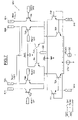
- FIG. 2 illustrates an embodiment of a totally differential architecture of an ETV stage. More precisely, this stage ETV comprises two cells, namely an analog multiplier cell CLM and an analog current routing cell CLA.
- the analog multiplier cell CLM comprises a pair of inputs ElA and ElB for receiving an input current comprising a DC component IMIXDC and a radio frequency dynamic component iin.
- the DC component IMIXDC is in fact the DC component of the output current of the mixer MD.
- the cell CLM comprises a pair of outputs S 1 B and S 1 A which also form the pair of inputs E 2 B and E 2 A of the current routing cell CLA.
- the cell CLM also comprises a controllable current source SC delivering a DC control current whose value is equal to 2*IGAIN.
- the cell CLM additionally comprises current multiplication means possessing a first pair of transistors T 1 A and T 1 B respectively connected between the input pair E 1 A and E 1 B and the supply terminal Vdd.
- the bases of these two transistors T 1 A and T 1 B are together linked to a voltage source STNE
- bipolar transistors are described, the embodiment of FIG. 2 could be envisaged with MOS transistors operating in identical current/voltage operating spans.
- the current multiplication means additionally comprises a second pair of bipolar transistors T 2 A and T 2 B.
- the emitters of these two transistors T 2 A and T 2 B are connected to the output of the controllable current source SC while the collectors of these transistors in fact form the output terminals S 1 B and S 1 A.
- the bases of these bipolar transistors T 2 A and T 2 B are respectively connected to the two inputs E 1 A and E 1 B, and consequently to the emitters of the two transistors T 1 A and T 1 B.
- the cell CLM delivers an output current having a DC component equal to IGAIN and a radio frequency dynamic component iout.
- This cell amplifies or attenuates the dynamic input current with a gain dependent on a ratio of DC currents. More precisely, the ratio iouit/iin of the output current to the input current is equal to the ratio IGAIN/IMIXDC of the DC components of the output and input currents.
- the ratio iout/iin is equal to the ratio between half the value of the DC control current (2*IGAIN) and the value of the DC component of the input current.
- the consumption of current of a mobile telephone will decrease when the output power requested decreases. Since most of the time the telephone operates at intermediate powers, the duration of communication can be increased.
- the current routing cell CLA comprises two inputs E 2 B and E 2 A, two outputs S 2 B and S 2 A and two control inputs GA and GB.
- the cell also comprises routing means comprising a fourth pair of transistors T 4 A and T 4 B respectively connected between the two inputs E 2 A and E 2 B and the supply terminal Vdd. The bases of these transistors T 4 A and T 4 B are linked to the control input GB.
- the routing means also comprise a fifth pair of transistors T 5 A and T 5 B respectively connected between the two inputs E 2 A and E 2 B and the two outputs S 2 A and S 2 B of the cell CLA. The bases of these two transistors T 5 A and T 5 B are linked to the control input GA.
- a voltage source ST making it possible to generate the various voltages on the control terminals GA and GB is conventional.
- the baseband processing means PBB which include means of control of the current source SC and of the voltage source ST, for example, embodied in the form of a software module or in hardware form, will act by priority on the value of the gain (or attenuation) of the multiplier cell CLM.
- the multiplier cell has a dynamic swing in gain of 60 dB to obtain an output power of 10 dBm (obtained for a load of 200 ohms at the output of the stage ETV)
- the value of the gain of the cell CLM will be fixed at 20 dB, for example, whereas the value of the gain of the current routing cell is fixed at 0 dB. This corresponds to a unit gain which is its maximum.
- the value of the gain of this cell When the value of the gain of this cell has reached its minimum value ( ⁇ 40 dB in the example), the value of the gain of the current routing cell is then decreased so as to descend progressively to ⁇ 30 dB and reach an output power of ⁇ 80 dBm.
- the CDMA2000 specification is then perfectly fulfilled in terms of noise and of ACPR, and is over a dynamic swing of 90 dB in gain while having a current consumption which decreases with power requested (curve C 3 ).
- FIG. 5 Reference is now made more particularly to FIG. 5 to describe another embodiment of the analog multiplier cell CLM. Only the differences between FIGS. 3 and 5 will be described for simplification purposes.
- the embodiment of FIG. 5 is not sensitive to the current gain ⁇ of the transistors, thereby making it possible to have optimized operation for high values of gain of the cell.
- the inputs E 1 A and E 1 B of the cell are formed by the collectors of the transistors T 1 A and T 1 B. Additionally, the collectors of these transistors are connected to the bases of these same transistors and these bases are respectively connected to the bases of the transistors T 2 A and T 2 B.
- the emitters of the transistors T 1 A and T 1 B are biased by a bias voltage source STP.
- This embodiment exhibits the same transfer function as that of the embodiment of FIG. 3 .
- FIG. 6 illustrates an embodiment making it possible to reuse, on command, the input current of the cell CLM, with the input current emanating from the mixer, for example.
- FIGS. 2 and 6 are identical to FIGS. 2 and 6 to illustrate an embodiment making it possible to reuse, on command, the input current of the cell CLM, with the input current emanating from the mixer, for example.
- FIG. 6 the current routing cell CLA, identical to that of FIG. 2 , has not been represented in detail.
- the multiplication cell CLM comprises a third pair of NPN bipolar transistors, T 3 A and T 3 B.
- the emitter of the transistors T 3 A is connected to the input E 1 A and to the base of the transistor T 2 A, whereas the emitter of the transistors T 3 B is connected to the input E 1 B and to the base of the transistor T 2 B.
- the collector of the transistor T 3 A is linked to the output S 2 A while the collector of the transistor T 3 B is connected to the output S 2 B.
- the bases of the transistors T 1 A and T 1 B are connected to a first state control input LG while the bases of the transistor T 3 A and T 3 B are connected to a second state control input HG.
- Control means MCM are then able to deliver respectively voltages LG and HG on the control inputs LG and HG. These voltages LG and HG act as state control signals.
- a first state for example, when the voltage LG is greater than the voltage HG, the transistors T 1 A and T 1 B are on and the transistors T 3 A and T 3 B are off. In this first state, the configuration of FIG. 2 therefore prevails again.
- the transistors T 1 A and T 1 B are off while the transistors T 3 A and T 3 B are on.
- the input current is summed at the output S 2 A and S 2 B of the stage ETV.
- the gain of the cell CLM then becomes equal to IGAIN/IMIXDC+1.
- the means MCM may be embodied in part in the baseband processing means PBB in regards to the digital part of the control, and in part by conventional logic circuits for the production of the logic control voltages.
- FIG. 7 Reference is now made more particularly to FIG. 7 to describe an embodiment compatible with its incorporation into a dual-band cellular mobile telephone, for example. Here again, only the differences relative to FIG. 2 will now be described.
- the output means of the current routing cell comprise two selectable different differential output pathways. More precisely, the outputs S 2 A and S 2 B form the output of a first differential pathway while the outputs S 3 A and S 3 B form the output of an additional differential pathway.
- the current routing means comprise a sixth pair of transistors T 6 A and T 6 B.
- the collectors of these transistors T 6 A and T 6 B are connected to the additional outputs S 3 A and S 3 B while the emitters of these transistors are connected, just like the emitters of the transistors T 5 A and T 5 B, to the emitters of the transistors T 4 A and T 4 B.
- the control inputs GA 1 are linked to the bases of the transistors T 5 A and T 5 B while the additional control inputs GA 2 are linked to the bases of the transistors T 6 A and T 6 B.
- the controllable voltage source comprises two blocks ST 1 , ST 2 capable of delivering the control voltages on the inputs GA 1 , GA 2 and GB.
- the voltage GA 2 will be chosen well below the smaller of the two voltages GA 1 and GB.
- a stage may be implemented in a dual-band telephone capable of operating for example according to the CELL standard or the PCS standard which exhibit different frequency bands.
- FIG. 7 is perfectly compatible with the embodiment of FIG. 6 , the characteristics of these two modes being combinable. It was shown above that the consumption of current of the stage decreased with the desired output power. The current emanating from the mixer may then become predominant.
- the gain of the mixer is decreased for example by around 10 dB and the gain of the multiplier cell is increased simultaneously by the same value. Thereafter, to further decrease the output power, the gain of the mixer is left unchanged (curve C 0 ) and the gain of the multiplier cell is decreased to its minimum (curve C 1 ) before possibly acting on the attenuation coefficient of the current routing cell (curve C 2 ).
- the invention just described has in particular the following advantages.
- the device fully satisfies the CDMA2000 specifications in terms of noise and ACPR over 90 dB of dynamic swing.
- the current consumption decreases linearly with output power without requiring any complex biasing scheme since a current source is used both to bias the stage and to adjust the gain.
- the input of the stage exhibits a low impedance, thereby improving the linearity of the mixer.
- the input of the stage may be completely differential, thereby rendering it not sensitive to common mode parasitic signals.
- the absence of any inductive element makes it possible to obtain reduced surface proportions and a reduction in parasitic magnetic emissions.
- the architecture is compatible with a radio frequency integrated technology, for example, a Bi-CMOS 0.25 micron technology and a cellular mobile telephone environment, for example, 3.1 volts on the battery and 9 dBm of maximum output power.
Abstract
Description
Claims (30)
Applications Claiming Priority (2)
| Application Number | Priority Date | Filing Date | Title |
|---|---|---|---|
| FR0510767A FR2892577B1 (en) | 2005-10-21 | 2005-10-21 | VARIABLE GAIN / ATTENUATION CONTROLLABLE RADIOFREQUENCE STAGE PARTICULARLY INCORPORATED IN THE TRANSMISSION CHAIN OF A CELLULAR MOBILE TELEPHONE, AND CORRESPONDING CONTROL METHOD |
| FR0510767 | 2005-10-21 |
Publications (2)
| Publication Number | Publication Date |
|---|---|
| US20070111683A1 US20070111683A1 (en) | 2007-05-17 |
| US7593700B2 true US7593700B2 (en) | 2009-09-22 |
Family
ID=36593765
Family Applications (1)
| Application Number | Title | Priority Date | Filing Date |
|---|---|---|---|
| US11/550,871 Expired - Fee Related US7593700B2 (en) | 2005-10-21 | 2006-10-19 | Controllable radio frequency stage with variable gain/attenuation, in particular incorporated into the transmission chain of a cellular mobile telephone, and corresponding control method |
Country Status (2)
| Country | Link |
|---|---|
| US (1) | US7593700B2 (en) |
| FR (1) | FR2892577B1 (en) |
Citations (9)
| Publication number | Priority date | Publication date | Assignee | Title |
|---|---|---|---|---|
| US5864255A (en) * | 1994-06-20 | 1999-01-26 | Unisearch Limited | Four quadrant square law analog multiplier using floating gate MOS transitions |
| EP1065785A2 (en) | 1999-06-29 | 2001-01-03 | Kabushiki Kaisha Toshiba | Transmission circuit and radio transmission apparatus |
| US6212369B1 (en) | 1998-06-05 | 2001-04-03 | Maxim Integrated Products, Inc. | Merged variable gain mixers |
| US20030045263A1 (en) | 2000-11-29 | 2003-03-06 | Myles Wakayama | Integrated direct conversion satellite tuner |
| US20030181189A1 (en) * | 1999-04-16 | 2003-09-25 | Sorrells David F. | Method and apparatus for reducing DC offsets in communication systems using universal frequency translation technology |
| US20040157568A1 (en) * | 2001-07-27 | 2004-08-12 | Michael Asam | Circuit arrangement for the regulation of a direct component of a signal and mobile radio transmitter |
| US20050143028A1 (en) * | 2003-12-24 | 2005-06-30 | Agency For Science, Technology And Research | DC offset-free RF front-end circuits and systems for direct conversion receivers |
| US7433658B1 (en) * | 2003-09-30 | 2008-10-07 | Marvell International Ltd. | System and method for controlling true output power of a transmitter |
| US7469137B2 (en) * | 2004-12-17 | 2008-12-23 | Broadcom Corporation | Radio receiver DC offset cancellation via ADC input bias |
-
2005
- 2005-10-21 FR FR0510767A patent/FR2892577B1/en active Active
-
2006
- 2006-10-19 US US11/550,871 patent/US7593700B2/en not_active Expired - Fee Related
Patent Citations (10)
| Publication number | Priority date | Publication date | Assignee | Title |
|---|---|---|---|---|
| US5864255A (en) * | 1994-06-20 | 1999-01-26 | Unisearch Limited | Four quadrant square law analog multiplier using floating gate MOS transitions |
| US6212369B1 (en) | 1998-06-05 | 2001-04-03 | Maxim Integrated Products, Inc. | Merged variable gain mixers |
| US20030181189A1 (en) * | 1999-04-16 | 2003-09-25 | Sorrells David F. | Method and apparatus for reducing DC offsets in communication systems using universal frequency translation technology |
| US7321751B2 (en) * | 1999-04-16 | 2008-01-22 | Parkervision, Inc. | Method and apparatus for improving dynamic range in a communication system |
| EP1065785A2 (en) | 1999-06-29 | 2001-01-03 | Kabushiki Kaisha Toshiba | Transmission circuit and radio transmission apparatus |
| US20030045263A1 (en) | 2000-11-29 | 2003-03-06 | Myles Wakayama | Integrated direct conversion satellite tuner |
| US20040157568A1 (en) * | 2001-07-27 | 2004-08-12 | Michael Asam | Circuit arrangement for the regulation of a direct component of a signal and mobile radio transmitter |
| US7433658B1 (en) * | 2003-09-30 | 2008-10-07 | Marvell International Ltd. | System and method for controlling true output power of a transmitter |
| US20050143028A1 (en) * | 2003-12-24 | 2005-06-30 | Agency For Science, Technology And Research | DC offset-free RF front-end circuits and systems for direct conversion receivers |
| US7469137B2 (en) * | 2004-12-17 | 2008-12-23 | Broadcom Corporation | Radio receiver DC offset cancellation via ADC input bias |
Also Published As
| Publication number | Publication date |
|---|---|
| FR2892577B1 (en) | 2008-01-25 |
| FR2892577A1 (en) | 2007-04-27 |
| US20070111683A1 (en) | 2007-05-17 |
Similar Documents
| Publication | Publication Date | Title |
|---|---|---|
| US7336127B2 (en) | Doherty amplifier configuration for a collector controlled power amplifier | |
| US6701138B2 (en) | Power amplifier control | |
| US6917246B2 (en) | Doherty bias circuit to dynamically compensate for process and environmental variations | |
| US7053706B2 (en) | High linearity doherty communication amplifier with bias control | |
| EP0673112B1 (en) | Power amplifier and power amplification method | |
| US6369649B2 (en) | Transmission power amplification method and apparatus | |
| US20190058444A1 (en) | Power amplifier module | |
| JP2004221646A (en) | Doherty amplifier | |
| US7710185B2 (en) | Tuneable circuit for canceling third order modulation | |
| US6731173B1 (en) | Doherty bias circuit to dynamically compensate for process and environmental variations | |
| KR100398754B1 (en) | Variable gain circuit | |
| RU2209504C2 (en) | High-dynamic-range variable-gain amplifier | |
| JP2004048581A (en) | Receiver and gain control system | |
| US20030048133A1 (en) | Wireless communication frequency signal amplification apparatus and transmitting and receiving apparatus | |
| EP0895350A1 (en) | Low power gain controlled amplifier with high dynamic range | |
| JP4252423B2 (en) | Variable amplifier and portable radio terminal using the same | |
| US20070018727A1 (en) | Variable gain amplifier and wireless communication apparatus including the same | |
| US7501887B2 (en) | Controllable amplifier and its use | |
| JP4312779B2 (en) | Variable amplifier and portable radio terminal using the same | |
| EP1532732A2 (en) | System and method for establishing the input impedance of an amplifier in a stacked configuration | |
| US11606066B2 (en) | Power amplifier circuit | |
| US7593700B2 (en) | Controllable radio frequency stage with variable gain/attenuation, in particular incorporated into the transmission chain of a cellular mobile telephone, and corresponding control method | |
| US7282995B2 (en) | Variable gain amplifier | |
| JP2006311623A5 (en) | ||
| KR100347213B1 (en) | Radio-frequency power amplifier of mobile communication equipment |
Legal Events
| Date | Code | Title | Description |
|---|---|---|---|
| AS | Assignment |
Owner name: STMICROELECTRONICS SA, FRANCE Free format text: ASSIGNMENT OF ASSIGNORS INTEREST;ASSIGNORS:CATHELIN, PHILIPPE;GRASSET, JEAN-CHARLES;REEL/FRAME:018822/0656;SIGNING DATES FROM 20061122 TO 20061123 Owner name: STMICROELECTRONICS SA,FRANCE Free format text: ASSIGNMENT OF ASSIGNORS INTEREST;ASSIGNORS:CATHELIN, PHILIPPE;GRASSET, JEAN-CHARLES;SIGNING DATES FROM 20061122 TO 20061123;REEL/FRAME:018822/0656 |
|
| STCF | Information on status: patent grant |
Free format text: PATENTED CASE |
|
| CC | Certificate of correction | ||
| FPAY | Fee payment |
Year of fee payment: 4 |
|
| AS | Assignment |
Owner name: ST WIRELESS SA, SWITZERLAND Free format text: ASSIGNMENT OF ASSIGNORS INTEREST;ASSIGNOR:STMICROELECTRONICS S.A. (FKA SGS-THOMSON MICROELECTRONICS S.A.);REEL/FRAME:037650/0697 Effective date: 20080728 |
|
| AS | Assignment |
Owner name: ST-ERICSSON SA, SWITZERLAND Free format text: CHANGE OF NAME;ASSIGNOR:ST WIRELESS SA;REEL/FRAME:037683/0128 Effective date: 20080714 Owner name: ST-ERICSSON SA, EN LIQUIDATION, SWITZERLAND Free format text: STATUS CHANGE-ENTITY IN LIQUIDATION;ASSIGNOR:ST-ERICSSON SA;REEL/FRAME:037739/0493 Effective date: 20150223 |
|
| FPAY | Fee payment |
Year of fee payment: 8 |
|
| FEPP | Fee payment procedure |
Free format text: MAINTENANCE FEE REMINDER MAILED (ORIGINAL EVENT CODE: REM.); ENTITY STATUS OF PATENT OWNER: LARGE ENTITY |
|
| LAPS | Lapse for failure to pay maintenance fees |
Free format text: PATENT EXPIRED FOR FAILURE TO PAY MAINTENANCE FEES (ORIGINAL EVENT CODE: EXP.); ENTITY STATUS OF PATENT OWNER: LARGE ENTITY |
|
| STCH | Information on status: patent discontinuation |
Free format text: PATENT EXPIRED DUE TO NONPAYMENT OF MAINTENANCE FEES UNDER 37 CFR 1.362 |
|
| FP | Lapsed due to failure to pay maintenance fee |
Effective date: 20210922 |