US7595091B2 - Method of forming multi-domain alignment layer - Google Patents
Method of forming multi-domain alignment layer Download PDFInfo
- Publication number
- US7595091B2 US7595091B2 US10/842,878 US84287804A US7595091B2 US 7595091 B2 US7595091 B2 US 7595091B2 US 84287804 A US84287804 A US 84287804A US 7595091 B2 US7595091 B2 US 7595091B2
- Authority
- US
- United States
- Prior art keywords
- mask
- substrate
- alignment layer
- alignment
- ion beam
- Prior art date
- Legal status (The legal status is an assumption and is not a legal conclusion. Google has not performed a legal analysis and makes no representation as to the accuracy of the status listed.)
- Expired - Fee Related, expires
Links
Images


Classifications
-
- G—PHYSICS
- G02—OPTICS
- G02F—OPTICAL DEVICES OR ARRANGEMENTS FOR THE CONTROL OF LIGHT BY MODIFICATION OF THE OPTICAL PROPERTIES OF THE MEDIA OF THE ELEMENTS INVOLVED THEREIN; NON-LINEAR OPTICS; FREQUENCY-CHANGING OF LIGHT; OPTICAL LOGIC ELEMENTS; OPTICAL ANALOGUE/DIGITAL CONVERTERS
- G02F1/00—Devices or arrangements for the control of the intensity, colour, phase, polarisation or direction of light arriving from an independent light source, e.g. switching, gating or modulating; Non-linear optics
- G02F1/01—Devices or arrangements for the control of the intensity, colour, phase, polarisation or direction of light arriving from an independent light source, e.g. switching, gating or modulating; Non-linear optics for the control of the intensity, phase, polarisation or colour
- G02F1/13—Devices or arrangements for the control of the intensity, colour, phase, polarisation or direction of light arriving from an independent light source, e.g. switching, gating or modulating; Non-linear optics for the control of the intensity, phase, polarisation or colour based on liquid crystals, e.g. single liquid crystal display cells
- G02F1/133—Constructional arrangements; Operation of liquid crystal cells; Circuit arrangements
- G02F1/1333—Constructional arrangements; Manufacturing methods
- G02F1/1337—Surface-induced orientation of the liquid crystal molecules, e.g. by alignment layers
- G02F1/13378—Surface-induced orientation of the liquid crystal molecules, e.g. by alignment layers by treatment of the surface, e.g. embossing, rubbing or light irradiation
-
- G—PHYSICS
- G02—OPTICS
- G02F—OPTICAL DEVICES OR ARRANGEMENTS FOR THE CONTROL OF LIGHT BY MODIFICATION OF THE OPTICAL PROPERTIES OF THE MEDIA OF THE ELEMENTS INVOLVED THEREIN; NON-LINEAR OPTICS; FREQUENCY-CHANGING OF LIGHT; OPTICAL LOGIC ELEMENTS; OPTICAL ANALOGUE/DIGITAL CONVERTERS
- G02F1/00—Devices or arrangements for the control of the intensity, colour, phase, polarisation or direction of light arriving from an independent light source, e.g. switching, gating or modulating; Non-linear optics
- G02F1/01—Devices or arrangements for the control of the intensity, colour, phase, polarisation or direction of light arriving from an independent light source, e.g. switching, gating or modulating; Non-linear optics for the control of the intensity, phase, polarisation or colour
- G02F1/13—Devices or arrangements for the control of the intensity, colour, phase, polarisation or direction of light arriving from an independent light source, e.g. switching, gating or modulating; Non-linear optics for the control of the intensity, phase, polarisation or colour based on liquid crystals, e.g. single liquid crystal display cells
- G02F1/133—Constructional arrangements; Operation of liquid crystal cells; Circuit arrangements
- G02F1/1333—Constructional arrangements; Manufacturing methods
- G02F1/1337—Surface-induced orientation of the liquid crystal molecules, e.g. by alignment layers
- G02F1/133753—Surface-induced orientation of the liquid crystal molecules, e.g. by alignment layers with different alignment orientations or pretilt angles on a same surface, e.g. for grey scale or improved viewing angle
Definitions
- the present invention relates to a method of forming an alignment layer of a liquid crystal display (LCD) device, and more particularly, to a method of forming a multi-domain alignment layer by irradiating ion beam.
- LCD liquid crystal display
- CTR cathode ray tube
- the display device With the development of electronic industries, the display device whose usage was limited to a TV Braun tube and so forth, has been expanded for use in a personal computer, a notebook, a wireless terminal, a vehicle instrument panel, an electronic display board and the like. Also, due to the development of information communication technology, since it is possible to transmit a large amount of image information, the importance on a next generation display device capable of processing and displaying the large amount of image information is constantly increasing.
- next generation display device Many requirements exist for such a next generation display device; the next generation display device must be lighter, slimmer, shorter and smaller, have a high luminance, a large-sized screen, a low power consumption and a low price.
- the LCD is recently gaining in popularity.
- the LCD has a higher resolution than other flat displays, and a fast response time considerable to that of the CRT in implementing a moving picture.
- the LCD Due to the high brightness, high contrast, low power consumption characteristics, the LCD is widely used in applications such as a monitor of a desktop computer, a monitor of a notebook computer, a television set, a television set for a vehicle, a navigation system and the like.
- Twisted nematic (TN) mode LCDs have become extremely popular and are widely used at the present time.
- directors of liquid crystal molecules adjacent to the lower substrate are perpendicular to directors of liquid crystal molecules adjacent to the upper substrate.
- liquid crystal molecules of the TN mode LCD When an electric field is not applied, liquid crystal molecules of the TN mode LCD have a structure in which longer axes of the liquid crystal molecules are twisted in a spiral fashion.
- the liquid crystal molecules have a pitch and are parallel to the substrate.
- one of the recently developed technologies to secure a wide viewing angle that has rapidly gained popularity is a multi-domain technology in which each unit pixel has regions with different alignment directions.
- the respective domains have different alignment directions of liquid crystal molecules, thereby improving the viewing angle.
- the alignment process used to uniformly align liquid crystal molecules is an important factor in determining the normal operation of an LCD and the uniform display characteristic of a picture. Much research has been performed on such alignment processes.
- FIGS. 1A through 1E A method of forming a multi-domain alignment layer according to the related art will now be described in more detail with reference to FIGS. 1A through 1E .
- the method includes coating a thin polymer film, dividing each unit pixel of the coated thin polymer film into multi-domains, aligning the divided multi-domains in different directions.
- the alignment layer is generally formed of a polyimide-based organic material, and is aligned by a rubbing method.
- the rubbing method includes: coating a polyimide-based organic material film on a substrate; vaporizing a solvent contained in the coated polyimide-based organic material film at a temperature of 60-80° C.; hardening the polyimide-based organic material film at a temperature of 80-200° C. to form a polyimide alignment layer; and rubbing the polyimide alignment layer using a rubbing cloth such as a velvet in a predetermined direction to form an alignment direction.
- an organic film is coated on a substrate 101 , and is rubbed in a right-handed direction of the drawing, thereby forming a first alignment layer 103 with a right-handed alignment direction.
- a positive photosensitive resin film 105 is coated on the first alignment layer 103 .
- a mask is arranged over the photosensitive resin film 105 , light is irradiated onto the mask, the photosensitive resin film 105 exposed to the light is developed and etched, thereby forming a predetermined pattern.
- the exposed portions of the first alignment layer 103 are rubbed in a left-handed direction, thereby having a left-handed alignment direction.
- the photosensitive resin film pattern 105 is removed, thereby forming the alignment layer with a multi-domain structure.
- the related art method of forming a multi-domain alignment layer using the rubbing method is complicated due to the use of the photolithography process.
- the alignment layer may be damaged by the use of developer, etchant and the like during the photolithography process. Such an alignment layer may show unstable characteristics.
- the present invention is directed to a method of forming a multi-domain alignment layer that substantially obviates one or more problems due to limitations and disadvantages of the related art.
- the present invention provides a method of forming a multi-domain alignment layer by irradiating an ion beam, in which a mask, which is patterned to have a predetermined opening condition and provides a proper ion beam irradiation direction, is designed, thereby obtaining the alignment layer fabricated by a simple process and having superior properties.
- a method of forming a multi-domain alignment layer in one embodiment comprises: forming an alignment layer on a substrate; aligning a mask having a transmission part and a shielding part over the substrate; and forming a first alignment direction and a second alignment direction in the alignment layer by irradiating an ion beam onto the substrate at an irradiation angle of ⁇ .
- FIGS. 1A through 1E are sectional views illustrating a method of forming a multi-domain alignment layer according to the related art
- FIGS. 2A through 2C are schematic views of a unit pixel with a multi-domain structure in an LCD according to the present invention.
- FIG. 3 is a plane view of a mask used in a process of forming an alignment layer by irradiating ion beam according to an embodiment of the present invention
- FIGS. 4A and 4B are sectional views schematically illustrating relationship between a mask and a substrate in irradiating ion beam so as to form a multi-domain alignment layer according to the present invention
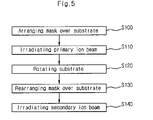
- FIG. 5 is a flow diagram illustrating a method of forming a multi-domain alignment layer according to an embodiment of the present invention.
- FIGS. 6A through 6D are sectional views schematically illustrating a method of forming a multi-domain alignment layer according to an embodiment of the present invention.
- FIGS. 2A through 2C are schematic views of a unit pixel with a multi-domain structure in an LCD according to the present invention.
- FIG. 2A corresponds to a unit pixel, which is divided and aligned into two domains
- FIG. 2B corresponds to a unit pixel, which is divided and aligned into four domains
- FIG. 2C is another embodiment of four domains alignment and corresponds to a unit pixel, which is divided and aligned into four domains.
- an LCD with a unit pixel consisting of two domains includes an upper substrate, a lower substrate opposing the upper substrate, and a liquid crystal layer interposed between the upper substrate and the lower substrate.
- each unit pixel on the upper substrate and the lower substrate is divided into two domains and the two domains are aligned in different directions.
- each unit pixel on the upper substrate and the lower substrate is divided into four domains, and first two divided domains are aligned in a first direction and second remaining two domains are aligned in a second direction different from the first direction.
- the first two domains and the second two domains are designed in a structure to compensate for each other.
- the viewing angle can be enhanced due to the different alignment directions of the liquid crystal molecules within a unit pixel.
- each unit pixel has a structure that the divided domains compensate for each other.
- FIG. 3 is a plan view of a mask used in a process of forming an alignment layer by irradiating ion beam according to an embodiment of the present invention.
- the mask 220 includes a transmission part 222 and a shielding part 224 to control transmission of ion beam.
- the shielding part 224 absorbs or reflects an ion beam such that the ion beam does not arrive on the substrate.
- the transmission part 222 is shaped in a slit.
- the transmission part 222 allows transmission of the ion beam, thereby aligning the alignment layer in a particular direction.
- a desired multi-domain structure may be formed.
- FIGS. 4A and 4B are sectional views schematically illustrating the relationship between the mask and substrate when irradiating the substrate with the ion beam so as to form a multi-domain alignment layer according to the present invention.
- an alignment layer 210 is formed on a substrate 200 .
- the mask 220 a has a pattern including a transmission part and a shielding part corresponding to multi-domains of a unit pixel.
- the mask 220 a is spaced apart by a predetermined distance from the substrate 200 .
- An ion beam 230 is irradiated onto the substrate 200 with a predetermined irradiation angle ( ⁇ ).
- the ion beam 230 arrives on the substrate 200 after passing through the transmission part or is shielded by the shielding part.
- the ion beam 230 that has passed through the transmission part of the mask 220 a and is irradiated on the substrate 200 aligns exposed portions of the alignment layer 210 in a predetermined direction.
- the mask 220 a should satisfy the above equation 1.
- equation 2 When equation 2 is satisfied by equation 1, the ion beam is irradiated in the form of a straight line, so that a sum of the transmission part of the mask 220 a and the shielding part of the mask 220 a becomes equal to the size of the pixel.
- the width w 1 of the transmission part of the mask 220 a can be expressed by equation 4 when considering a margin X shielded by the thickness D of the mask 220 a in the size L/ 2 of the alignment layer aligned by the ion beam 230 passing through the transmission part at an irradiation angle.
- the ion beam 230 is irradiated onto the substrate 200 after the substrate 200 is rotated or the mask 220 a is moved.
- the above equations 1 through 4 should be satisfied.
- first portions of the alignment layer 210 are aligned in a first direction by irradiating an ion beam onto the substrate 200 using the mask 220 a arranged as shown in FIG. 4A
- the mask 220 b is rearranged as shown in FIG. 4B and the ion beam is again irradiated onto the substrate, so that second portions of the alignment layer 210 , which are not exposed to the ion beam during the first irradiation, are aligned in a second direction opposite to the first direction.
- the mask 220 b since the mask 220 b has the thickness D and the ion beam 230 is irradiated with an irradiation angle ⁇ , the mask 220 b is shifted to a direction parallel to the substrate in consideration of the thickness of the mask and the irradiation angle of the ion beam and rearranged to a new position.
- the ion beam is irradiated onto the substrate 200 , so that the second portions of the alignment layer 210 are aligned in the second direction.
- the two domains of each unit pixel which are aligned in different directions, have an identical size of L/ 2 .
- the irradiation angle ⁇ of the ion beam 230 and the width w 1 of the transmission part of the mask 220 b may be obtained as follows:
- the irradiation angle ⁇ of the ion beam is expressed by the equation below:
- the width w 1 of the transmission part of the mask has a relationship of
- FIG. 5 is a flow diagram illustrating a method of forming a multi-domain alignment layer according to an embodiment of the present invention
- FIGS. 6A through 6D are sectional views schematically illustrating a method of forming a multi-domain alignment layer according to an embodiment of the present invention.
- a substrate 200 for an LCD is prepared and a mask 220 a having predetermined patterns is arranged spaced apart from the substrate 200 by a predetermined interval (S 100 ).
- the substrate 200 has TFTs or color filters formed thereon.
- a tilt angle of liquid crystal molecule is determined by inclining the substrate 200 with respect to an irradiated ion beam by a predetermined angle.
- an alignment layer 210 is formed on the substrate 200 .
- the mask 220 a has predetermined slit pattern that is formed corresponding to multi-divided areas with respect to a unit pixel of the substrate 200 .
- the mask 220 a is arranged spaced apart from the substrate 200 by a predetermined interval.
- the substrate 200 is loaded on an ion beam irradiation apparatus, and a primary ion beam 230 is irradiated onto the substrate 200 (S 110 ).
- the irradiated ion beam 230 passes through the mask 220 a having the slit pattern and reach the substrate 200 .
- the alignment layer 210 exposed to the ion beams 230 is aligned in a predetermined direction.
- the alignment layer 210 formed of organic material such as polyimide is formed on the substrate 200 , the polyimide is divided into a main chain and a side chain in view of a chemical structure.
- the main chain functions to align liquid crystal molecules in a single alignment direction and the side chain functions to form a tilt angle.
- the alignment layer 210 may be formed of an inorganic material such as SiO 2 , SiC, Si 3 N 4 , Al 2 O 3 , CeO 2 , SnO 2 , glass, ZnTiO 2 , diamond-like carbon (DLC), or the like.
- an inorganic material such as SiO 2 , SiC, Si 3 N 4 , Al 2 O 3 , CeO 2 , SnO 2 , glass, ZnTiO 2 , diamond-like carbon (DLC), or the like.
- the mask 220 a includes the slit pattern that has a predetermined transmission part and a predetermined shielding part.
- the alignment layer 210 is aligned on only some divided areas of the pixel cell due to the ion beams 230 , which pass through the slit of the mask 220 a.
- the irradiated primary ion beam 230 is shielded and the substrate 200 is then rotated (S 120 ).
- the substrate 200 may be rotated up and down.
- the substrate 200 inclined with respect to the irradiated ion beams 230 is arranged inclined in an opposite direction.
- a mask 220 b that is arranged spaced apart from the substrate 200 is re-arranged (S 130 ).
- the mask 220 b has a slit pattern and may shield a secondary ion beam that is irradiated on the areas aligned due to the primary ion beam at the alignment layer 210 .
- the mask 220 a used in the irradiation of the primary ion beams may be used as the mask 220 b by shifting the mask 220 a .
- another mask may be used as the mask 220 b by spacing it apart from the substrate 200 and re-arranging it.
- the substrate 200 is re-arranged in the above manner and secondary ion beams 230 are irradiated (S 140 ).
- the irradiated secondary ion beam 230 passes through the mask 220 b having the slit pattern and reach the substrate 200 .
- the alignment layer 210 exposed to the secondary ion beam 230 is aligned in a predetermined direction.
- the ion beams 230 passing through the slit of the mask 220 b cause only some divided areas of the unit pixel to be aligned in a direction opposite to an alignment direction formed in the irradiation of the primary ion beam.
- the alignment direction formed by irradiating the primary ion beam onto the alignment layer 210 is opposite to that formed by irradiating the secondary ion beam.
- the mask having an appropriate thickness, transmission part and shielding part is arranged at a front of the alignment layer. Then, relations among width of the transmission part of the mask, pixel size, thickness of the mask, distance between the alignment layer and the mask, and ion beam irradiation angle are provided.
- the multi-alignment process may be performed effectively, thereby simplifying the manufacturing process and reducing the manufacturing cost.
Abstract
Description
Claims (42)
Applications Claiming Priority (2)
| Application Number | Priority Date | Filing Date | Title |
|---|---|---|---|
| KRP2003-30643 | 2003-05-14 | ||
| KR1020030030643A KR100845410B1 (en) | 2003-05-14 | 2003-05-14 | A method of forming an multi-domain alignment layer |
Publications (2)
| Publication Number | Publication Date |
|---|---|
| US20040227883A1 US20040227883A1 (en) | 2004-11-18 |
| US7595091B2 true US7595091B2 (en) | 2009-09-29 |
Family
ID=33411716
Family Applications (1)
| Application Number | Title | Priority Date | Filing Date |
|---|---|---|---|
| US10/842,878 Expired - Fee Related US7595091B2 (en) | 2003-05-14 | 2004-05-10 | Method of forming multi-domain alignment layer |
Country Status (2)
| Country | Link |
|---|---|
| US (1) | US7595091B2 (en) |
| KR (1) | KR100845410B1 (en) |
Families Citing this family (15)
| Publication number | Priority date | Publication date | Assignee | Title |
|---|---|---|---|---|
| US6967340B2 (en) * | 2003-08-19 | 2005-11-22 | Alps Electric Co., Ltd. | Ion beam irradiation device and operating method thereof |
| KR100845714B1 (en) * | 2003-12-30 | 2008-07-10 | 엘지디스플레이 주식회사 | Device and fabrication method for liquid crystal display of multi domain |
| KR101112558B1 (en) | 2005-06-15 | 2012-02-15 | 재단법인서울대학교산학협력재단 | Liquid crystal display |
| JP4113547B2 (en) * | 2005-12-12 | 2008-07-09 | インターナショナル・ビジネス・マシーンズ・コーポレーション | Alignment layer forming apparatus and alignment layer forming method |
| US8593602B2 (en) * | 2006-04-27 | 2013-11-26 | Sharp Kabushiki Kaisha | Production method for liquid crystal display device and exposure device including exposure of alignment layers |
| TW200827818A (en) * | 2006-12-29 | 2008-07-01 | Tpo Displays Corp | Systems for displaying images |
| CN101344684B (en) * | 2007-07-12 | 2011-12-28 | 北京京东方光电科技有限公司 | Substrate of LCD device and manufacturing method thereof |
| KR101279538B1 (en) * | 2008-02-19 | 2013-06-28 | 엘지디스플레이 주식회사 | Method of aligning alingment layer and OCB mode LCD device having alingment layer aligned through the method |
| KR100930426B1 (en) * | 2008-02-19 | 2009-12-08 | 하이디스 테크놀로지 주식회사 | Ion Beam Irradiation Device for Forming Orientation Pattern |
| KR101448007B1 (en) | 2008-04-01 | 2014-10-08 | 삼성디스플레이 주식회사 | Method of manufacturing liquid crystal display |
| KR101469035B1 (en) | 2008-05-28 | 2014-12-11 | 삼성디스플레이 주식회사 | Method of manufacturing liquid crystal display |
| KR100954968B1 (en) * | 2008-09-19 | 2010-04-23 | 하이디스 테크놀로지 주식회사 | Screen of ion beam apparatus |
| KR101698803B1 (en) | 2010-06-11 | 2017-02-02 | 삼성디스플레이 주식회사 | A liquid crystal display |
| JP5682232B2 (en) * | 2010-10-29 | 2015-03-11 | ソニー株式会社 | Liquid crystal light control device and imaging apparatus |
| CN105572973B (en) * | 2015-12-23 | 2018-10-09 | 南京中电熊猫液晶显示科技有限公司 | A kind of mask plate and light alignment method |
Citations (15)
| Publication number | Priority date | Publication date | Assignee | Title |
|---|---|---|---|---|
| US5030322A (en) | 1989-08-28 | 1991-07-09 | Sharp Kabushiki Kaisha | Method of forming orientation film of liquid-crystal display device |
| US5623354A (en) * | 1994-02-10 | 1997-04-22 | International Business Machines Corporation | Liquid crystal display with multi-domains |
| JPH09230351A (en) | 1996-02-21 | 1997-09-05 | Nissin Electric Co Ltd | Alignment layer treatment for alignment layer |
| US5770826A (en) | 1996-05-10 | 1998-06-23 | International Business Machines Corporation | Atomic beam alignment of liquid crystals |
| KR100230532B1 (en) | 1996-05-10 | 1999-11-15 | 포만 제프리 엘 | Method and apparatus for forming an alignment pattern on a surface |
| US6020946A (en) | 1998-02-23 | 2000-02-01 | International Business Machines Corporation | Dry processing for liquid-crystal displays using low energy ion bombardment |
| US6061115A (en) | 1998-11-03 | 2000-05-09 | International Business Machines Incorporation | Method of producing a multi-domain alignment layer by bombarding ions of normal incidence |
| US6061114A (en) * | 1998-02-23 | 2000-05-09 | International Business Machines Corporation | Alignment of liquid crystal layers |
| US6195146B1 (en) | 1996-05-10 | 2001-02-27 | International Business Machines Corporation | Tilted liquid crystal alignment produced by ion beam treatment on the alignment layer using a voltage less than 200v |
| US6313896B1 (en) * | 1999-08-31 | 2001-11-06 | International Business Machines Corporation | Method for forming a multi-domain alignment layer for a liquid crystal display device |
| US6331381B1 (en) | 2000-04-14 | 2001-12-18 | International Business Machines Corporation | Method for making a liquid crystal alignment layer |
| US6346975B2 (en) | 1998-08-04 | 2002-02-12 | International Business Machines Corporation | Liquid crystal display having alignment layer using ion bombarded amorphous material 100Å thickness or less |
| US20030059724A1 (en) * | 1999-10-14 | 2003-03-27 | Choi Young Seok | Method for manufacturing multi-domain liquid crystal cell |
| US20030142257A1 (en) * | 2002-01-28 | 2003-07-31 | International Business Machines Corporation | Multi-domain low twist angle liquid crystal cells and methods of production thereof |
| KR101003722B1 (en) | 2006-01-17 | 2010-12-24 | 무라타 기카이 가부시키가이샤 | Tray conveyance system |
-
2003
- 2003-05-14 KR KR1020030030643A patent/KR100845410B1/en active IP Right Grant
-
2004
- 2004-05-10 US US10/842,878 patent/US7595091B2/en not_active Expired - Fee Related
Patent Citations (16)
| Publication number | Priority date | Publication date | Assignee | Title |
|---|---|---|---|---|
| US5030322A (en) | 1989-08-28 | 1991-07-09 | Sharp Kabushiki Kaisha | Method of forming orientation film of liquid-crystal display device |
| US5623354A (en) * | 1994-02-10 | 1997-04-22 | International Business Machines Corporation | Liquid crystal display with multi-domains |
| JPH09230351A (en) | 1996-02-21 | 1997-09-05 | Nissin Electric Co Ltd | Alignment layer treatment for alignment layer |
| US6124914A (en) | 1996-05-10 | 2000-09-26 | International Business Machines Corporation | Method an apparatus for forming an alignment pattern on a surface using a particle beam useful for a liquid crystal |
| KR100230532B1 (en) | 1996-05-10 | 1999-11-15 | 포만 제프리 엘 | Method and apparatus for forming an alignment pattern on a surface |
| US5770826A (en) | 1996-05-10 | 1998-06-23 | International Business Machines Corporation | Atomic beam alignment of liquid crystals |
| US6195146B1 (en) | 1996-05-10 | 2001-02-27 | International Business Machines Corporation | Tilted liquid crystal alignment produced by ion beam treatment on the alignment layer using a voltage less than 200v |
| US6020946A (en) | 1998-02-23 | 2000-02-01 | International Business Machines Corporation | Dry processing for liquid-crystal displays using low energy ion bombardment |
| US6061114A (en) * | 1998-02-23 | 2000-05-09 | International Business Machines Corporation | Alignment of liquid crystal layers |
| US6346975B2 (en) | 1998-08-04 | 2002-02-12 | International Business Machines Corporation | Liquid crystal display having alignment layer using ion bombarded amorphous material 100Å thickness or less |
| US6061115A (en) | 1998-11-03 | 2000-05-09 | International Business Machines Incorporation | Method of producing a multi-domain alignment layer by bombarding ions of normal incidence |
| US6313896B1 (en) * | 1999-08-31 | 2001-11-06 | International Business Machines Corporation | Method for forming a multi-domain alignment layer for a liquid crystal display device |
| US20030059724A1 (en) * | 1999-10-14 | 2003-03-27 | Choi Young Seok | Method for manufacturing multi-domain liquid crystal cell |
| US6331381B1 (en) | 2000-04-14 | 2001-12-18 | International Business Machines Corporation | Method for making a liquid crystal alignment layer |
| US20030142257A1 (en) * | 2002-01-28 | 2003-07-31 | International Business Machines Corporation | Multi-domain low twist angle liquid crystal cells and methods of production thereof |
| KR101003722B1 (en) | 2006-01-17 | 2010-12-24 | 무라타 기카이 가부시키가이샤 | Tray conveyance system |
Non-Patent Citations (1)
| Title |
|---|
| Office Action for Corresponding Korean Patent Application Serial No. 9-5-2007-040818194. |
Also Published As
| Publication number | Publication date |
|---|---|
| KR100845410B1 (en) | 2008-07-10 |
| KR20040098327A (en) | 2004-11-20 |
| US20040227883A1 (en) | 2004-11-18 |
Similar Documents
| Publication | Publication Date | Title |
|---|---|---|
| US7595091B2 (en) | Method of forming multi-domain alignment layer | |
| US8767156B2 (en) | Production method of liquid crystal display device with halftone overlapping masking and liquid crystal display device | |
| US7499136B2 (en) | Liquid crystal display device | |
| JP5400176B2 (en) | Exposure apparatus and method of manufacturing liquid crystal display device | |
| US7528911B2 (en) | Liquid crystal display device and method of manufacturing the same | |
| US20080297708A1 (en) | Liquid crystal display panel, electronic apparatus, and manufacturing method thereof | |
| US6271904B1 (en) | Liquid crystal display having bump structures | |
| US7420638B2 (en) | Liquid crystal display device with mask for alignment | |
| US20170082894A1 (en) | Liquid crystal display device, optical control member, and base material for manufacturing optical control member | |
| WO2016152330A1 (en) | Liquid crystal display device | |
| JP2000250045A (en) | Liquid crystal display device and its production | |
| US20210072601A1 (en) | Aligning Method for Liquid Crystal Panel, Liquid Crystal Panel and Display Device | |
| US20110304808A1 (en) | Liquid crystal display | |
| CN104520761A (en) | Liquid crystal display device | |
| US7400375B2 (en) | Method for designing mask and fabricating panel | |
| US7430031B2 (en) | Liquid crystal display device and method of fabricating the same | |
| JP2005227745A (en) | Liquid crystal display device and electronic apparatus | |
| US7067224B2 (en) | Method for fabricating a liquid crystal display device | |
| US7683992B2 (en) | Multi-domain liquid crystal display | |
| US6535260B1 (en) | Liquid crystal display device | |
| KR20040083181A (en) | A method of forming an multi-domain alignment layer | |
| US5790221A (en) | Method of manufacturing a liquid crystal cell | |
| KR0155201B1 (en) | Alignment film forming method of lcd | |
| JP2007018014A (en) | Liquid crystal display device and electronic apparatus | |
| KR20040083127A (en) | A method of forming an alignment layer by irradiating ion beam |
Legal Events
| Date | Code | Title | Description |
|---|---|---|---|
| AS | Assignment |
Owner name: LG. PHILIPS LCD CO., LTD., KOREA, REPUBLIC OF Free format text: ASSIGNMENT OF ASSIGNORS INTEREST;ASSIGNORS:LEE, YUN BOK;SHIN, KYEONG A;HAM, YONG SUNG;REEL/FRAME:015321/0948 Effective date: 20040504 |
|
| AS | Assignment |
Owner name: LG DISPLAY CO., LTD., KOREA, REPUBLIC OF Free format text: CHANGE OF NAME;ASSIGNOR:LG PHILIPS LCD CO., LTD.;REEL/FRAME:020986/0231 Effective date: 20080229 Owner name: LG DISPLAY CO., LTD.,KOREA, REPUBLIC OF Free format text: CHANGE OF NAME;ASSIGNOR:LG PHILIPS LCD CO., LTD.;REEL/FRAME:020986/0231 Effective date: 20080229 |
|
| STCF | Information on status: patent grant |
Free format text: PATENTED CASE |
|
| FEPP | Fee payment procedure |
Free format text: PAYOR NUMBER ASSIGNED (ORIGINAL EVENT CODE: ASPN); ENTITY STATUS OF PATENT OWNER: LARGE ENTITY |
|
| FEPP | Fee payment procedure |
Free format text: PAYER NUMBER DE-ASSIGNED (ORIGINAL EVENT CODE: RMPN); ENTITY STATUS OF PATENT OWNER: LARGE ENTITY Free format text: PAYOR NUMBER ASSIGNED (ORIGINAL EVENT CODE: ASPN); ENTITY STATUS OF PATENT OWNER: LARGE ENTITY |
|
| CC | Certificate of correction | ||
| CC | Certificate of correction | ||
| FPAY | Fee payment |
Year of fee payment: 4 |
|
| FPAY | Fee payment |
Year of fee payment: 8 |
|
| FEPP | Fee payment procedure |
Free format text: MAINTENANCE FEE REMINDER MAILED (ORIGINAL EVENT CODE: REM.); ENTITY STATUS OF PATENT OWNER: LARGE ENTITY |
|
| LAPS | Lapse for failure to pay maintenance fees |
Free format text: PATENT EXPIRED FOR FAILURE TO PAY MAINTENANCE FEES (ORIGINAL EVENT CODE: EXP.); ENTITY STATUS OF PATENT OWNER: LARGE ENTITY |
|
| STCH | Information on status: patent discontinuation |
Free format text: PATENT EXPIRED DUE TO NONPAYMENT OF MAINTENANCE FEES UNDER 37 CFR 1.362 |
|
| FP | Lapsed due to failure to pay maintenance fee |
Effective date: 20210929 |