US7602119B2 - OLED with magenta and green emissive layers - Google Patents
OLED with magenta and green emissive layers Download PDFInfo
- Publication number
- US7602119B2 US7602119B2 US11/315,827 US31582705A US7602119B2 US 7602119 B2 US7602119 B2 US 7602119B2 US 31582705 A US31582705 A US 31582705A US 7602119 B2 US7602119 B2 US 7602119B2
- Authority
- US
- United States
- Prior art keywords
- green
- emitting layer
- red
- light
- light emitting
- Prior art date
- Legal status (The legal status is an assumption and is not a legal conclusion. Google has not performed a legal analysis and makes no representation as to the accuracy of the status listed.)
- Active, expires
Links
- 0 [1*]C([2*])([3*])[4*] Chemical compound [1*]C([2*])([3*])[4*] 0.000 description 13
- BLGXPNUXTJZYPK-GDNGEXCGSA-M CC1=C[O-][Mn+]N1.CC1=N[Mn+][O-]C1 Chemical compound CC1=C[O-][Mn+]N1.CC1=N[Mn+][O-]C1 BLGXPNUXTJZYPK-GDNGEXCGSA-M 0.000 description 2
- CEZVFJLUYDPZBX-UHFFFAOYSA-N C1=CC2=CC3=C(C=CC=C3)C(C3=CC4=C(C=CC=C4)C=C3)=C2C=C1.CC1=CC=C(C2=CC=C([Si](C)(C)C)C=C2)C=C1 Chemical compound C1=CC2=CC3=C(C=CC=C3)C(C3=CC4=C(C=CC=C4)C=C3)=C2C=C1.CC1=CC=C(C2=CC=C([Si](C)(C)C)C=C2)C=C1 CEZVFJLUYDPZBX-UHFFFAOYSA-N 0.000 description 1
- DDAWMGINEUZRME-UHFFFAOYSA-N C1=CC2=CC=C(C3=CC=CC(C4=C5C=CC=CC5=C(C5=CC=C6C=CC=CC6=C5)C5=C4C=CC=C5)=C3)C=C2C=C1.C1=CC=C(C2=CC(C3=C4C=CC=CC4=C(C4=CC=C5C=CC=CC5=C4)C4=C3C=CC=C4)=CC(C3=CC4=C(C=CC=C4)C=C3)=C2)C=C1.C1=CC=C(C2=CC(C3=CC=CC=C3)=C(C3=C4C=CC=CC4=C(C4=CC5=C/C=C/C=C\5C=C4)C4=C3C=CC=C4)C=C2)C=C1 Chemical compound C1=CC2=CC=C(C3=CC=CC(C4=C5C=CC=CC5=C(C5=CC=C6C=CC=CC6=C5)C5=C4C=CC=C5)=C3)C=C2C=C1.C1=CC=C(C2=CC(C3=C4C=CC=CC4=C(C4=CC=C5C=CC=CC5=C4)C4=C3C=CC=C4)=CC(C3=CC4=C(C=CC=C4)C=C3)=C2)C=C1.C1=CC=C(C2=CC(C3=CC=CC=C3)=C(C3=C4C=CC=CC4=C(C4=CC5=C/C=C/C=C\5C=C4)C4=C3C=CC=C4)C=C2)C=C1 DDAWMGINEUZRME-UHFFFAOYSA-N 0.000 description 1
- ZYIHEEYFRHDLNX-UHFFFAOYSA-N C1=CC=C(C2=C(C3=C4C=CC=CC4=C(C4=CC=C5C=CC=CC5=C4)C4=C3C=CC=C4)C=CC=C2)C=C1.C1=CC=C(C2=CC=C(C3=C4C=CC=CC4=C(C4=CC=C5C=CC=CC5=C4)C4=C3C=CC=C4)C=C2)C=C1.C1=CC=C(C2=CC=C(C3=C4C=CC=CC4=C(C4=CC=CC5=C4C=CC=C5)C4=C3C=CC=C4)C=C2)C=C1 Chemical compound C1=CC=C(C2=C(C3=C4C=CC=CC4=C(C4=CC=C5C=CC=CC5=C4)C4=C3C=CC=C4)C=CC=C2)C=C1.C1=CC=C(C2=CC=C(C3=C4C=CC=CC4=C(C4=CC=C5C=CC=CC5=C4)C4=C3C=CC=C4)C=C2)C=C1.C1=CC=C(C2=CC=C(C3=C4C=CC=CC4=C(C4=CC=CC5=C4C=CC=C5)C4=C3C=CC=C4)C=C2)C=C1 ZYIHEEYFRHDLNX-UHFFFAOYSA-N 0.000 description 1
- WPPDXAHGCGPUPK-UHFFFAOYSA-N C1=CC=C(C2=C3C=CC=CC3=C(C3=CC=CC=C3)C3=C2C2=CC=C4C5=C2/C3=C\C=C/5C2=CC=C3C5=C(C6=CC=CC=C6)C6=C(C=CC=C6)C(C6=CC=CC=C6)=C5/C5=C/C=C/4C2=C35)C=C1 Chemical compound C1=CC=C(C2=C3C=CC=CC3=C(C3=CC=CC=C3)C3=C2C2=CC=C4C5=C2/C3=C\C=C/5C2=CC=C3C5=C(C6=CC=CC=C6)C6=C(C=CC=C6)C(C6=CC=CC=C6)=C5/C5=C/C=C/4C2=C35)C=C1 WPPDXAHGCGPUPK-UHFFFAOYSA-N 0.000 description 1
- GBQWTDIDGUCJNT-UHFFFAOYSA-N C1=CC=C(C2=CC(C3=C4C=CC=CC4=C(C4=CC5=C(C=CC=C5)C=C4)C4=C3C=CC=C4)=CC=C2)C=C1.C1=CC=C(C2=CC=C(C3=C4C=CC=CC4=C(/C4=C/C=C5/C6=CC=CC=C6C6=CC=CC4=C65)C4=C3C=CC=C4)C=C2)C=C1.C1=CC=C(C2=CC=C(C3=C4C=CC=CC4=C(C4=CC=CC5=C4C=CC4=C5C=CC=C4)C4=C3C=CC=C4)C=C2)C=C1 Chemical compound C1=CC=C(C2=CC(C3=C4C=CC=CC4=C(C4=CC5=C(C=CC=C5)C=C4)C4=C3C=CC=C4)=CC=C2)C=C1.C1=CC=C(C2=CC=C(C3=C4C=CC=CC4=C(/C4=C/C=C5/C6=CC=CC=C6C6=CC=CC4=C65)C4=C3C=CC=C4)C=C2)C=C1.C1=CC=C(C2=CC=C(C3=C4C=CC=CC4=C(C4=CC=CC5=C4C=CC4=C5C=CC=C4)C4=C3C=CC=C4)C=C2)C=C1 GBQWTDIDGUCJNT-UHFFFAOYSA-N 0.000 description 1
- GHBOAMGPGVIWSP-UHFFFAOYSA-N C1=CC=C(C2=CC(C3=C4C=CC=CC4=C(C4=CC=C5C=CC=CC5=C4)C4=C3C=CC=C4)=CC(C3=C4C=CC=CC4=CC=C3)=C2)C=C1.C1=CC=C(C2=CC(C3=CC=CC=C3)=CC(C3=C4C=CC=CC4=C(C4=CC=CC5=C4C=CC=C5)C4=C3C=CC=C4)=C2)C=C1.CC1=CC=C(C2=C3C=CC=CC3=C(C3=CC=C(C4=CC=C(F)C=C4)C=C3)C3=C2C=CC=C3)C2=C1C=CC=C2 Chemical compound C1=CC=C(C2=CC(C3=C4C=CC=CC4=C(C4=CC=C5C=CC=CC5=C4)C4=C3C=CC=C4)=CC(C3=C4C=CC=CC4=CC=C3)=C2)C=C1.C1=CC=C(C2=CC(C3=CC=CC=C3)=CC(C3=C4C=CC=CC4=C(C4=CC=CC5=C4C=CC=C5)C4=C3C=CC=C4)=C2)C=C1.CC1=CC=C(C2=C3C=CC=CC3=C(C3=CC=C(C4=CC=C(F)C=C4)C=C3)C3=C2C=CC=C3)C2=C1C=CC=C2 GHBOAMGPGVIWSP-UHFFFAOYSA-N 0.000 description 1
- IBDNXIIXCFFPDL-UHFFFAOYSA-N C1=CC=C(C2=CC(C3=C4C=CC=CC4=C(C4=CC=CC5=C4C=CC=C5)C4=C3C=CC=C4)=CC=C2)C=C1.C1=CC=C(C2=CC=C(C3=C4C=CC=CC4=C(C4=CC5=C(C=C4)C4=C(C=CC=C4)C=C5)C4=C3C=CC=C4)C=C2)C=C1.C1=CC=C(C2=CC=C(C3=CC(C4=C5C=CC=CC5=C(C5=CC=C6C=CC=CC6=C5)C5=C4C=CC=C5)=CC=C3)C=C2)C=C1 Chemical compound C1=CC=C(C2=CC(C3=C4C=CC=CC4=C(C4=CC=CC5=C4C=CC=C5)C4=C3C=CC=C4)=CC=C2)C=C1.C1=CC=C(C2=CC=C(C3=C4C=CC=CC4=C(C4=CC5=C(C=C4)C4=C(C=CC=C4)C=C5)C4=C3C=CC=C4)C=C2)C=C1.C1=CC=C(C2=CC=C(C3=CC(C4=C5C=CC=CC5=C(C5=CC=C6C=CC=CC6=C5)C5=C4C=CC=C5)=CC=C3)C=C2)C=C1 IBDNXIIXCFFPDL-UHFFFAOYSA-N 0.000 description 1
- SWRBCSOLMPPRPD-UHFFFAOYSA-N C1=CC=C(C2=CC(C3=CC=CC=C3)=CC(C3=C4C=CC=CC4=C(C4=CC5=C6C7=C4/C=C\C=C/7C=C/C6=C/C=C\5)C4=C3C=CC=C4)=C2)C=C1.CC1=C2C=CC=CC2=C(C2=CC=C(C3=CC=CC=C3)C3=C2C=CC=C3)C2=C1C=CC=C2.FC(F)(F)C1=CC=C(C2=CC=CC=C2)C=C1.N#CC1=CC=C(C2=CC=C(C3=C4C=CC=CC4=C(C4=CC=CC5=C4C=CC=C5)C4=C3C=CC=C4)C=C2)C=C1 Chemical compound C1=CC=C(C2=CC(C3=CC=CC=C3)=CC(C3=C4C=CC=CC4=C(C4=CC5=C6C7=C4/C=C\C=C/7C=C/C6=C/C=C\5)C4=C3C=CC=C4)=C2)C=C1.CC1=C2C=CC=CC2=C(C2=CC=C(C3=CC=CC=C3)C3=C2C=CC=C3)C2=C1C=CC=C2.FC(F)(F)C1=CC=C(C2=CC=CC=C2)C=C1.N#CC1=CC=C(C2=CC=C(C3=C4C=CC=CC4=C(C4=CC=CC5=C4C=CC=C5)C4=C3C=CC=C4)C=C2)C=C1 SWRBCSOLMPPRPD-UHFFFAOYSA-N 0.000 description 1
- YHVKHTIGOYNLKN-UHFFFAOYSA-N C1=CC=C(C2=CC(C3=CC=CC=C3)=CC(C3=C4C=CC=CC4=C(C4=CC=C5C=CC=CC5=C4)C4=C3C=CC=C4)=C2)C=C1.CC1=CC(C)=C(C2=CC=C(C3=C4C=CC=CC4=C(C4=CC=C5C=CC=CC5=C4)C4=C3C=CC=C4)C=C2)C(C)=C1.CC1=CC(C2=CC=CC=C2)=CC(C)=C1C1=C2C=CC=CC2=C(C2=CC=C3C=CC=CC3=C2)C2=C1C=CC=C2 Chemical compound C1=CC=C(C2=CC(C3=CC=CC=C3)=CC(C3=C4C=CC=CC4=C(C4=CC=C5C=CC=CC5=C4)C4=C3C=CC=C4)=C2)C=C1.CC1=CC(C)=C(C2=CC=C(C3=C4C=CC=CC4=C(C4=CC=C5C=CC=CC5=C4)C4=C3C=CC=C4)C=C2)C(C)=C1.CC1=CC(C2=CC=CC=C2)=CC(C)=C1C1=C2C=CC=CC2=C(C2=CC=C3C=CC=CC3=C2)C2=C1C=CC=C2 YHVKHTIGOYNLKN-UHFFFAOYSA-N 0.000 description 1
- HSPKWQAZHXHTNA-UHFFFAOYSA-N C1=CC=C(C2=CC=CC(C3=CC=C(C4=C5C=CC=CC5=C(C5=CC=C6C=CC=CC6=C5)C5=C4C=CC=C5)C=C3)=C2)C=C1.CC1=CC(C)=C(C2=CC=CC(C3=C4C=CC=CC4=C(C4=CC=C5C=CC=CC5=C4)C4=C3C=CC=C4)=C2)C(C)=C1.C[Si](C)(C)C1=CC(C2=CC=C(C3=C4C=CC=CC4=C(C4=CC5=C(C=CC=C5)C=C4)C4=C3C=CC=C4)C=C2)=CC=C1 Chemical compound C1=CC=C(C2=CC=CC(C3=CC=C(C4=C5C=CC=CC5=C(C5=CC=C6C=CC=CC6=C5)C5=C4C=CC=C5)C=C3)=C2)C=C1.CC1=CC(C)=C(C2=CC=CC(C3=C4C=CC=CC4=C(C4=CC=C5C=CC=CC5=C4)C4=C3C=CC=C4)=C2)C(C)=C1.C[Si](C)(C)C1=CC(C2=CC=C(C3=C4C=CC=CC4=C(C4=CC5=C(C=CC=C5)C=C4)C4=C3C=CC=C4)C=C2)=CC=C1 HSPKWQAZHXHTNA-UHFFFAOYSA-N 0.000 description 1
- MLUILYSCPAXSNM-UHFFFAOYSA-N CB1(C)N2C=CC=CC2=NC2=CC=CC=N21.CC.CC Chemical compound CB1(C)N2C=CC=CC2=NC2=CC=CC=N21.CC.CC MLUILYSCPAXSNM-UHFFFAOYSA-N 0.000 description 1
- VGPZXQDVQZJEBS-UHFFFAOYSA-N CC(C1)C1C1C(C)CCCC1 Chemical compound CC(C1)C1C1C(C)CCCC1 VGPZXQDVQZJEBS-UHFFFAOYSA-N 0.000 description 1
- REAYQGOJSVIUHD-UHFFFAOYSA-N CC1(C)CCN2CCC(C)(C)C3=C2C1=CC1=C3OC(=O)C(C2=NC3=CC=CC=C3S2)=C1.CC1=CC(C)=C2N=C(C3=CC4=C(OC3=O)C3=C5C(=C4)C(C)(C)CCN5CCC3(C)C)SC2=C1.CCN(CC)C1=CC2=C(C=C1)C=C(C1=NC3=C(C)C=C(C)C=C3S1)C(=O)O2.CCN(CC)C1=CC2=C(C=C1)C=C(C1=NC3=CC=CC=C3O1)C(=O)O2 Chemical compound CC1(C)CCN2CCC(C)(C)C3=C2C1=CC1=C3OC(=O)C(C2=NC3=CC=CC=C3S2)=C1.CC1=CC(C)=C2N=C(C3=CC4=C(OC3=O)C3=C5C(=C4)C(C)(C)CCN5CCC3(C)C)SC2=C1.CCN(CC)C1=CC2=C(C=C1)C=C(C1=NC3=C(C)C=C(C)C=C3S1)C(=O)O2.CCN(CC)C1=CC2=C(C=C1)C=C(C1=NC3=CC=CC=C3O1)C(=O)O2 REAYQGOJSVIUHD-UHFFFAOYSA-N 0.000 description 1
- UXVWSJSRMODDHH-UHFFFAOYSA-N CC1=C(C)C(C)=C2C(=C1C)C1=C(C)C(C)=C3C4=C1/C2=C(C)\C(C)=C/4C1=C(C)C(C)=C2C4=C(C(C)=C(C)C(C)=C4C)/C4=C(C)/C(C)=C/3C1=C24 Chemical compound CC1=C(C)C(C)=C2C(=C1C)C1=C(C)C(C)=C3C4=C1/C2=C(C)\C(C)=C/4C1=C(C)C(C)=C2C4=C(C(C)=C(C)C(C)=C4C)/C4=C(C)/C(C)=C/3C1=C24 UXVWSJSRMODDHH-UHFFFAOYSA-N 0.000 description 1
- WAUZOROLVOAXID-UHFFFAOYSA-N CC1=CC(C)=C(C2=CC=C3C(=C2)C=CC2=N3B(F)(F)N3C(=N2)C=CC2=C3C=CC(C3=C(C)C=C(C)C=C3C)=C2)C(C)=C1.CC1=CC(C)=C(C2=CC=C3C(=C2)C=CC2=N3B(F)(F)N3C=C(C4=CC=CC=C4)C4=C(C=CC=C4)C3=N2)C(C)=C1 Chemical compound CC1=CC(C)=C(C2=CC=C3C(=C2)C=CC2=N3B(F)(F)N3C(=N2)C=CC2=C3C=CC(C3=C(C)C=C(C)C=C3C)=C2)C(C)=C1.CC1=CC(C)=C(C2=CC=C3C(=C2)C=CC2=N3B(F)(F)N3C=C(C4=CC=CC=C4)C4=C(C=CC=C4)C3=N2)C(C)=C1 WAUZOROLVOAXID-UHFFFAOYSA-N 0.000 description 1
- LQYYDWJDEVKDGB-XPWSMXQVSA-N CC1=CC=C(N(C2=CC=C(C)C=C2)C2=CC=C(/C=C/C3=CC=C(/C=C/C4=CC=C(N(C5=CC=C(C)C=C5)C5=CC=C(C)C=C5)C=C4)C=C3)C=C2)C=C1 Chemical compound CC1=CC=C(N(C2=CC=C(C)C=C2)C2=CC=C(/C=C/C3=CC=C(/C=C/C4=CC=C(N(C5=CC=C(C)C=C5)C5=CC=C(C)C=C5)C=C4)C=C3)C=C2)C=C1 LQYYDWJDEVKDGB-XPWSMXQVSA-N 0.000 description 1
- ATUOYWHBWRKTHZ-UHFFFAOYSA-N CCC Chemical compound CCC ATUOYWHBWRKTHZ-UHFFFAOYSA-N 0.000 description 1
- NCRUNZDGCISBJZ-UHFFFAOYSA-N CN1C2=CC3=C(C=C2C(=O)C2=C1C=C(F)C=C2)N(C)C1=C(C=CC(F)=C1)C3=O.CN1C2=CC3=C(C=C2C(=O)C2=C1C=CC=C2)N(C)C1=C(C=CC=C1)C3=O.O=C1C2=CC3=C(C=C2N(C2=CC=CC=C2)C2=C1C=CC=C2)C(=O)C1=C(C=CC=C1)N3C1=CC=CC=C1 Chemical compound CN1C2=CC3=C(C=C2C(=O)C2=C1C=C(F)C=C2)N(C)C1=C(C=CC(F)=C1)C3=O.CN1C2=CC3=C(C=C2C(=O)C2=C1C=CC=C2)N(C)C1=C(C=CC=C1)C3=O.O=C1C2=CC3=C(C=C2N(C2=CC=CC=C2)C2=C1C=CC=C2)C(=O)C1=C(C=CC=C1)N3C1=CC=CC=C1 NCRUNZDGCISBJZ-UHFFFAOYSA-N 0.000 description 1
- KCGXOYXIYZCECE-OXIHZCFMSA-N Cc1ccc(N(c2ccc(C)cc2)c2ccc(-c3ccc(/C=C/c4ccc5cc(N(c6ccc(C)cc6)c6ccc(C)cc6)ccc5c4)cc3)cc2)cc1.Cc1ccc(N(c2ccc(C)cc2)c2ccc(-c3ccc4cc(/C=C/c5ccc6cc(N(c7ccc(C)cc7)c7ccc(C)cc7)ccc6c5)ccc4c3)cc2)cc1.Cc1ccc(N(c2ccc(C)cc2)c2ccc(/C=C/c3ccc(-c4ccc(N(c5ccc(C)cc5)c5ccc(C)cc5)cc4)cc3)cc2)cc1.Cc1ccc(N(c2ccc(C)cc2)c2ccc(/C=C/c3ccc(-c4ccc5cc(N(c6ccc(C)cc6)c6ccc(C)cc6)ccc5c4)cc3)cc2)cc1.Cc1ccc(N(c2ccc(C)cc2)c2ccc(/C=C/c3ccc4cc(-c5ccc(N(c6ccc(C)cc6)c6ccc(C)cc6)cc5)ccc4c3)cc2)cc1 Chemical compound Cc1ccc(N(c2ccc(C)cc2)c2ccc(-c3ccc(/C=C/c4ccc5cc(N(c6ccc(C)cc6)c6ccc(C)cc6)ccc5c4)cc3)cc2)cc1.Cc1ccc(N(c2ccc(C)cc2)c2ccc(-c3ccc4cc(/C=C/c5ccc6cc(N(c7ccc(C)cc7)c7ccc(C)cc7)ccc6c5)ccc4c3)cc2)cc1.Cc1ccc(N(c2ccc(C)cc2)c2ccc(/C=C/c3ccc(-c4ccc(N(c5ccc(C)cc5)c5ccc(C)cc5)cc4)cc3)cc2)cc1.Cc1ccc(N(c2ccc(C)cc2)c2ccc(/C=C/c3ccc(-c4ccc5cc(N(c6ccc(C)cc6)c6ccc(C)cc6)ccc5c4)cc3)cc2)cc1.Cc1ccc(N(c2ccc(C)cc2)c2ccc(/C=C/c3ccc4cc(-c5ccc(N(c6ccc(C)cc6)c6ccc(C)cc6)cc5)ccc4c3)cc2)cc1 KCGXOYXIYZCECE-OXIHZCFMSA-N 0.000 description 1
- KZZYQMQMHLVTHM-UHFFFAOYSA-N FB1(F)N2C(=NC3=N1C1=CC=CC=C1C(C1=CC=CC=C1)=C3)C=C(C1=CC=CC=C1)C1=C2C=CC=C1.FB1(F)N2C(=NC3=N1C1=CC=CC=C1C(C1=CC=CC=C1)=C3C1=CC=CC=C1)C=CC1=C2C=CC=C1.FB1(F)N2C(=NC3=N1C1=CC=CC=C1C=C3C1=CC=CC=C1)C=CC1=C2C=CC=C1.FB1(F)N2C=CC3=C(C=CC=C3)C2=NC2=N1C1=CC=CC=C1C(C1=CC=CC=C1)=C2.FB1(F)N2C=CC3=C(C=CC=C3)C2=NC2=N1C1=CC=CC=C1C=C2C1=CC=CC=C1 Chemical compound FB1(F)N2C(=NC3=N1C1=CC=CC=C1C(C1=CC=CC=C1)=C3)C=C(C1=CC=CC=C1)C1=C2C=CC=C1.FB1(F)N2C(=NC3=N1C1=CC=CC=C1C(C1=CC=CC=C1)=C3C1=CC=CC=C1)C=CC1=C2C=CC=C1.FB1(F)N2C(=NC3=N1C1=CC=CC=C1C=C3C1=CC=CC=C1)C=CC1=C2C=CC=C1.FB1(F)N2C=CC3=C(C=CC=C3)C2=NC2=N1C1=CC=CC=C1C(C1=CC=CC=C1)=C2.FB1(F)N2C=CC3=C(C=CC=C3)C2=NC2=N1C1=CC=CC=C1C=C2C1=CC=CC=C1 KZZYQMQMHLVTHM-UHFFFAOYSA-N 0.000 description 1
- YPOZHTGQGDZBOB-WFQQYQPKSA-N [C-]#[N+]/C(C#N)=C1/C=C(/C=C/C2=CC3=C4C(=C2)CC(C)(C)CN4CC(C)(C)C3)OC(C(C)(C)C)=C1 Chemical compound [C-]#[N+]/C(C#N)=C1/C=C(/C=C/C2=CC3=C4C(=C2)CC(C)(C)CN4CC(C)(C)C3)OC(C(C)(C)C)=C1 YPOZHTGQGDZBOB-WFQQYQPKSA-N 0.000 description 1
- OJPZYFHUIJLHGF-SISBMOCJSA-N [C-]#[N+]/C(C#N)=C1\C=C(C)OC(/C=C/C2=CC([Y][Y][Y])=C(N([Y])[Y][Y])C([Y][Y][Y][Y][Y])=C2)=C1 Chemical compound [C-]#[N+]/C(C#N)=C1\C=C(C)OC(/C=C/C2=CC([Y][Y][Y])=C(N([Y])[Y][Y])C([Y][Y][Y][Y][Y])=C2)=C1 OJPZYFHUIJLHGF-SISBMOCJSA-N 0.000 description 1
Images


Classifications
-
- C—CHEMISTRY; METALLURGY
- C09—DYES; PAINTS; POLISHES; NATURAL RESINS; ADHESIVES; COMPOSITIONS NOT OTHERWISE PROVIDED FOR; APPLICATIONS OF MATERIALS NOT OTHERWISE PROVIDED FOR
- C09K—MATERIALS FOR MISCELLANEOUS APPLICATIONS, NOT PROVIDED FOR ELSEWHERE
- C09K11/00—Luminescent, e.g. electroluminescent, chemiluminescent materials
- C09K11/06—Luminescent, e.g. electroluminescent, chemiluminescent materials containing organic luminescent materials
-
- H—ELECTRICITY
- H05—ELECTRIC TECHNIQUES NOT OTHERWISE PROVIDED FOR
- H05B—ELECTRIC HEATING; ELECTRIC LIGHT SOURCES NOT OTHERWISE PROVIDED FOR; CIRCUIT ARRANGEMENTS FOR ELECTRIC LIGHT SOURCES, IN GENERAL
- H05B33/00—Electroluminescent light sources
- H05B33/12—Light sources with substantially two-dimensional radiating surfaces
- H05B33/14—Light sources with substantially two-dimensional radiating surfaces characterised by the chemical or physical composition or the arrangement of the electroluminescent material, or by the simultaneous addition of the electroluminescent material in or onto the light source
-
- H—ELECTRICITY
- H10—SEMICONDUCTOR DEVICES; ELECTRIC SOLID-STATE DEVICES NOT OTHERWISE PROVIDED FOR
- H10K—ORGANIC ELECTRIC SOLID-STATE DEVICES
- H10K59/00—Integrated devices, or assemblies of multiple devices, comprising at least one organic light-emitting element covered by group H10K50/00
- H10K59/30—Devices specially adapted for multicolour light emission
- H10K59/38—Devices specially adapted for multicolour light emission comprising colour filters or colour changing media [CCM]
-
- C—CHEMISTRY; METALLURGY
- C09—DYES; PAINTS; POLISHES; NATURAL RESINS; ADHESIVES; COMPOSITIONS NOT OTHERWISE PROVIDED FOR; APPLICATIONS OF MATERIALS NOT OTHERWISE PROVIDED FOR
- C09K—MATERIALS FOR MISCELLANEOUS APPLICATIONS, NOT PROVIDED FOR ELSEWHERE
- C09K2211/00—Chemical nature of organic luminescent or tenebrescent compounds
- C09K2211/10—Non-macromolecular compounds
- C09K2211/1003—Carbocyclic compounds
- C09K2211/1007—Non-condensed systems
-
- C—CHEMISTRY; METALLURGY
- C09—DYES; PAINTS; POLISHES; NATURAL RESINS; ADHESIVES; COMPOSITIONS NOT OTHERWISE PROVIDED FOR; APPLICATIONS OF MATERIALS NOT OTHERWISE PROVIDED FOR
- C09K—MATERIALS FOR MISCELLANEOUS APPLICATIONS, NOT PROVIDED FOR ELSEWHERE
- C09K2211/00—Chemical nature of organic luminescent or tenebrescent compounds
- C09K2211/10—Non-macromolecular compounds
- C09K2211/1003—Carbocyclic compounds
- C09K2211/1011—Condensed systems
-
- C—CHEMISTRY; METALLURGY
- C09—DYES; PAINTS; POLISHES; NATURAL RESINS; ADHESIVES; COMPOSITIONS NOT OTHERWISE PROVIDED FOR; APPLICATIONS OF MATERIALS NOT OTHERWISE PROVIDED FOR
- C09K—MATERIALS FOR MISCELLANEOUS APPLICATIONS, NOT PROVIDED FOR ELSEWHERE
- C09K2211/00—Chemical nature of organic luminescent or tenebrescent compounds
- C09K2211/10—Non-macromolecular compounds
- C09K2211/1003—Carbocyclic compounds
- C09K2211/1014—Carbocyclic compounds bridged by heteroatoms, e.g. N, P, Si or B
-
- C—CHEMISTRY; METALLURGY
- C09—DYES; PAINTS; POLISHES; NATURAL RESINS; ADHESIVES; COMPOSITIONS NOT OTHERWISE PROVIDED FOR; APPLICATIONS OF MATERIALS NOT OTHERWISE PROVIDED FOR
- C09K—MATERIALS FOR MISCELLANEOUS APPLICATIONS, NOT PROVIDED FOR ELSEWHERE
- C09K2211/00—Chemical nature of organic luminescent or tenebrescent compounds
- C09K2211/10—Non-macromolecular compounds
- C09K2211/1018—Heterocyclic compounds
- C09K2211/1025—Heterocyclic compounds characterised by ligands
- C09K2211/1029—Heterocyclic compounds characterised by ligands containing one nitrogen atom as the heteroatom
- C09K2211/1033—Heterocyclic compounds characterised by ligands containing one nitrogen atom as the heteroatom with oxygen
-
- C—CHEMISTRY; METALLURGY
- C09—DYES; PAINTS; POLISHES; NATURAL RESINS; ADHESIVES; COMPOSITIONS NOT OTHERWISE PROVIDED FOR; APPLICATIONS OF MATERIALS NOT OTHERWISE PROVIDED FOR
- C09K—MATERIALS FOR MISCELLANEOUS APPLICATIONS, NOT PROVIDED FOR ELSEWHERE
- C09K2211/00—Chemical nature of organic luminescent or tenebrescent compounds
- C09K2211/10—Non-macromolecular compounds
- C09K2211/1018—Heterocyclic compounds
- C09K2211/1025—Heterocyclic compounds characterised by ligands
- C09K2211/1029—Heterocyclic compounds characterised by ligands containing one nitrogen atom as the heteroatom
- C09K2211/1037—Heterocyclic compounds characterised by ligands containing one nitrogen atom as the heteroatom with sulfur
-
- C—CHEMISTRY; METALLURGY
- C09—DYES; PAINTS; POLISHES; NATURAL RESINS; ADHESIVES; COMPOSITIONS NOT OTHERWISE PROVIDED FOR; APPLICATIONS OF MATERIALS NOT OTHERWISE PROVIDED FOR
- C09K—MATERIALS FOR MISCELLANEOUS APPLICATIONS, NOT PROVIDED FOR ELSEWHERE
- C09K2211/00—Chemical nature of organic luminescent or tenebrescent compounds
- C09K2211/10—Non-macromolecular compounds
- C09K2211/1018—Heterocyclic compounds
- C09K2211/1025—Heterocyclic compounds characterised by ligands
- C09K2211/1044—Heterocyclic compounds characterised by ligands containing two nitrogen atoms as heteroatoms
-
- C—CHEMISTRY; METALLURGY
- C09—DYES; PAINTS; POLISHES; NATURAL RESINS; ADHESIVES; COMPOSITIONS NOT OTHERWISE PROVIDED FOR; APPLICATIONS OF MATERIALS NOT OTHERWISE PROVIDED FOR
- C09K—MATERIALS FOR MISCELLANEOUS APPLICATIONS, NOT PROVIDED FOR ELSEWHERE
- C09K2211/00—Chemical nature of organic luminescent or tenebrescent compounds
- C09K2211/10—Non-macromolecular compounds
- C09K2211/1018—Heterocyclic compounds
- C09K2211/1025—Heterocyclic compounds characterised by ligands
- C09K2211/1059—Heterocyclic compounds characterised by ligands containing three nitrogen atoms as heteroatoms
- C09K2211/107—Heterocyclic compounds characterised by ligands containing three nitrogen atoms as heteroatoms with other heteroatoms
-
- C—CHEMISTRY; METALLURGY
- C09—DYES; PAINTS; POLISHES; NATURAL RESINS; ADHESIVES; COMPOSITIONS NOT OTHERWISE PROVIDED FOR; APPLICATIONS OF MATERIALS NOT OTHERWISE PROVIDED FOR
- C09K—MATERIALS FOR MISCELLANEOUS APPLICATIONS, NOT PROVIDED FOR ELSEWHERE
- C09K2211/00—Chemical nature of organic luminescent or tenebrescent compounds
- C09K2211/10—Non-macromolecular compounds
- C09K2211/1018—Heterocyclic compounds
- C09K2211/1025—Heterocyclic compounds characterised by ligands
- C09K2211/1088—Heterocyclic compounds characterised by ligands containing oxygen as the only heteroatom
-
- H—ELECTRICITY
- H10—SEMICONDUCTOR DEVICES; ELECTRIC SOLID-STATE DEVICES NOT OTHERWISE PROVIDED FOR
- H10K—ORGANIC ELECTRIC SOLID-STATE DEVICES
- H10K50/00—Organic light-emitting devices
- H10K50/10—OLEDs or polymer light-emitting diodes [PLED]
- H10K50/11—OLEDs or polymer light-emitting diodes [PLED] characterised by the electroluminescent [EL] layers
- H10K50/125—OLEDs or polymer light-emitting diodes [PLED] characterised by the electroluminescent [EL] layers specially adapted for multicolour light emission, e.g. for emitting white light
-
- H—ELECTRICITY
- H10—SEMICONDUCTOR DEVICES; ELECTRIC SOLID-STATE DEVICES NOT OTHERWISE PROVIDED FOR
- H10K—ORGANIC ELECTRIC SOLID-STATE DEVICES
- H10K59/00—Integrated devices, or assemblies of multiple devices, comprising at least one organic light-emitting element covered by group H10K50/00
- H10K59/30—Devices specially adapted for multicolour light emission
- H10K59/35—Devices specially adapted for multicolour light emission comprising red-green-blue [RGB] subpixels
- H10K59/351—Devices specially adapted for multicolour light emission comprising red-green-blue [RGB] subpixels comprising more than three subpixels, e.g. red-green-blue-white [RGBW]
-
- H—ELECTRICITY
- H10—SEMICONDUCTOR DEVICES; ELECTRIC SOLID-STATE DEVICES NOT OTHERWISE PROVIDED FOR
- H10K—ORGANIC ELECTRIC SOLID-STATE DEVICES
- H10K71/00—Manufacture or treatment specially adapted for the organic devices covered by this subclass
- H10K71/60—Forming conductive regions or layers, e.g. electrodes
-
- H—ELECTRICITY
- H10—SEMICONDUCTOR DEVICES; ELECTRIC SOLID-STATE DEVICES NOT OTHERWISE PROVIDED FOR
- H10K—ORGANIC ELECTRIC SOLID-STATE DEVICES
- H10K85/00—Organic materials used in the body or electrodes of devices covered by this subclass
- H10K85/30—Coordination compounds
- H10K85/321—Metal complexes comprising a group IIIA element, e.g. Tris (8-hydroxyquinoline) gallium [Gaq3]
- H10K85/324—Metal complexes comprising a group IIIA element, e.g. Tris (8-hydroxyquinoline) gallium [Gaq3] comprising aluminium, e.g. Alq3
-
- H—ELECTRICITY
- H10—SEMICONDUCTOR DEVICES; ELECTRIC SOLID-STATE DEVICES NOT OTHERWISE PROVIDED FOR
- H10K—ORGANIC ELECTRIC SOLID-STATE DEVICES
- H10K85/00—Organic materials used in the body or electrodes of devices covered by this subclass
- H10K85/40—Organosilicon compounds, e.g. TIPS pentacene
-
- H—ELECTRICITY
- H10—SEMICONDUCTOR DEVICES; ELECTRIC SOLID-STATE DEVICES NOT OTHERWISE PROVIDED FOR
- H10K—ORGANIC ELECTRIC SOLID-STATE DEVICES
- H10K85/00—Organic materials used in the body or electrodes of devices covered by this subclass
- H10K85/60—Organic compounds having low molecular weight
- H10K85/611—Charge transfer complexes
-
- H—ELECTRICITY
- H10—SEMICONDUCTOR DEVICES; ELECTRIC SOLID-STATE DEVICES NOT OTHERWISE PROVIDED FOR
- H10K—ORGANIC ELECTRIC SOLID-STATE DEVICES
- H10K85/00—Organic materials used in the body or electrodes of devices covered by this subclass
- H10K85/60—Organic compounds having low molecular weight
- H10K85/615—Polycyclic condensed aromatic hydrocarbons, e.g. anthracene
-
- H—ELECTRICITY
- H10—SEMICONDUCTOR DEVICES; ELECTRIC SOLID-STATE DEVICES NOT OTHERWISE PROVIDED FOR
- H10K—ORGANIC ELECTRIC SOLID-STATE DEVICES
- H10K85/00—Organic materials used in the body or electrodes of devices covered by this subclass
- H10K85/60—Organic compounds having low molecular weight
- H10K85/631—Amine compounds having at least two aryl rest on at least one amine-nitrogen atom, e.g. triphenylamine
-
- H—ELECTRICITY
- H10—SEMICONDUCTOR DEVICES; ELECTRIC SOLID-STATE DEVICES NOT OTHERWISE PROVIDED FOR
- H10K—ORGANIC ELECTRIC SOLID-STATE DEVICES
- H10K85/00—Organic materials used in the body or electrodes of devices covered by this subclass
- H10K85/60—Organic compounds having low molecular weight
- H10K85/649—Aromatic compounds comprising a hetero atom
Definitions
- the present invention relates to organic light emitting diode (OLED) displays. More specifically, this invention relates to multicolor OLED displays having three or more pixels with improved power efficiency.
- OLED organic light emitting diode
- OLED organic light emitting diodes
- an OLED is comprised of an anode for hole injection, a cathode for electron injection, and an organic media sandwiched between these electrodes to support charge recombination that yields emission of light.
- a plurality of individually addressable OLED elements are arranged in a matrix of pixels. Each pixel includes an independently addressable OLED and is capable of producing light.
- Such matrixes can be of the passive type where electroluminescent OLED layers are sandwiched between two sets of orthogonal electrodes (rows and columns).
- An example of a passive matrix driven OLED display device is described in U.S. Pat. No.
- the OLED display can be constructed of the active matrix type where one or more circuit elements, such as a transistor or capacitor, is used to drive each OLED.
- circuit elements such as a transistor or capacitor
- An example of an active matrix driven OLED display device is described in U.S. Pat. No. 5,550,066.
- a multicolor display In order to construct a multicolor display, the pixels are arranged to produce a variety of colors.
- a multicolor display can be constructed to have red, green, and blue pixels.
- Such a display is referred to as an RGB display. Additional colors can be achieved by such a display by mixing the light emitted by the red, green, and blue subpixels in various ratios.
- the human eye is less sensitive to light emitted by the red pixels or the blue pixels compared to light emitted by the green pixels.
- One effect of this attribute is that the human eye is less sensitive to spatial detail within the red and blue color channels and therefore it is known to use pixel patterns having fewer red and blue pixels as described in U.S. Pat. No. 5,113,274.
- the use of fewer red and blue pixels than green pixels is particularly useful when the spatial position of the red and blue subpixels are alternated along both rows and columns within the array of pixels.
- OLED electroluminescent layers for each of the pixels. This results in the need to pattern one or more of the OLED electroluminescent layers such that it is precisely aligned with the desired pixel.
- OLED layers can be deposited through a shadow mask in order to selectively deposit only in the desired areas. Shadow masks should then be aligned with the target pixel. Such alignment processes, however, are more complicated and can slow manufacturing throughput.
- Shadow masks also tend to cause damage to the OLED pixels when the mask contacts the display substrate.
- Alternate methods of separately patterning OLED layers for each layer are also known. For example, a method of pattering the OLED layers by transferring the OLED material from a donor sheet by use of a laser is known. However, this method requires the use of consumable donor substrates and complex laser writing equipment. The process of writing each pixel with a laser can also reduce manufacturing throughput.
- Another example process for patterning OLED layers involves deposition of the OLED materials dissolved in a solvent as droplets by way of an ink jet print head. This method requires the precision placement of the ink jet droplets. As such, complex structures for controlling droplet placement and spread can be required and tolerances for the pixel area can be large.
- Yet another approach for constructing displays is to use a broadband white emitting OLED combined with R, G, and B color filters.
- This method reduces the need for precisely aligning or patterning the OLED layers, and the color filters can be pre-patterned using conventional photolithography techniques.
- this method results in a display with higher power consumption because the color filters absorb a significant amount of the light.
- an OLED display having at least red, green, and blue colored pixels comprising:
- a magenta light emitting layer provided over a substrate for red and blue pixels and a green light emitting layer provided over the substrate for producing at least a green pixel;
- first and second color filters in operative relationship with the magenta light-emitting layer to respectively produce red and blue pixels.
- the present invention provides a multicolor OLED display having at least three different color pixels that can be made more effectively.
- a feature of the present invention is that multicolor OLED displays made in accordance with the present invention can provide displays with a large color gamut at improved power efficiency.
- FIG. 1 shows a multicolor OLED display having three differently colored pixels as known in the prior art
- FIG. 2 shows a topside view of a group of pixels according to the first embodiment of the present invention
- FIG. 3 shows a cross section view of a group of pixels taken along the line 3 - 3 ′ of FIG. 2 ;
- FIG. 4 shows a plot of the spectral transmittance of two narrowband color filters as a function of wavelength as known in the prior art
- FIG. 5 shows a plot of a the relative emission of a magenta light emitting layer, as well as, the spectral transmittance of two broadband color filters as a function of wavelength;
- FIG. 6 shows a multicolor OLED display having two different pixel groups, each having three differently colored pixels as known in the prior art
- FIG. 7 shows a top side view of two different pixel groups useful in forming the display of FIG. 6 ;
- FIG. 8 shows a multicolor OLED display having four differently colored pixels
- FIG. 9 shows a top side view of a group of pixels useful in forming the display of FIG. 8 ;
- FIG. 10 shows a cross section view of a group of pixels taken along the line 6 - 6 ′ of FIG. 9 ;
- FIG. 11 shows a top side view of a another group of pixels useful in forming the display of FIG. 8 ;
- FIG. 12 shows a cross section view of a group of pixels taken along the line 9 - 9 ′ of FIG. 11 .
- FIG. 1 shows an example of a multicolor OLED display including three pixels that produce different colored light emission.
- pixel 11 a preferably produces red light
- pixel 11 b preferably produces green light
- pixel 11 c preferably produces blue light.
- These pixels can be arranged in groups, such as pixel group 10 . Although it is shown that each pixel group includes each of the differently colored pixels, the present invention is not limited to this case. Instead, some colored pixels can be present in greater number than other colored pixels.
- the short wavelength or blue portion of the visible spectrum generally will refer to a range of wavelengths within the visible spectrum with wavelengths shorter than 500 nm.
- the middle wavelength or green portion of the visible spectrum will generally refer to a range of wavelengths between 500 and 600 nm.
- the long or red portion of the visible spectrum will include wavelengths that are within the visible spectrum but that generally have wavelengths longer than 600 nm.
- FIG. 2 shows a top side view of pixels 11 a , 11 b , and 11 c according to the first embodiment of the present invention.
- these pixels can be addressed by providing a matrix of orthogonal electrodes such as first electrodes 110 a , 110 b , and 110 c and second electrode 130 . That is, pixel 11 a is constructed from first electrode 110 a and second electrode 130 , pixel 11 b is constructed from first electrode 110 b and second electrode 130 , and pixel 11 c is constructed from first electrode 110 c and second electrode 130 .
- all pixels in a column share the same first electrode and all pixels in a row share the same second electrode.
- these pixels are arranged into a stripe pattern.
- the present invention is not limited to this arrangement and other arrangements such as delta pattern arrangements and quad arrangements can be applied by one skilled in the art.
- the present invention is not limited to the passive matrix configuration and an active matrix driving scheme can be applied by one skilled in the art.
- magenta light emitting layer 123 a is provided for pixels 11 a and 11 b to be common between both of these pixels. This requires light emitting layer 123 a to be precisely aligned or patterned to these pixels. Green light emitting layer 123 c is provided for pixel 11 c and also requires a precise alignment or patterning step. In this manner, the number of precision aligned depositions required to form these three differently colored pixels is reduced from three to two. Magenta light emitting layer 123 a can be formed from a single step, such as for example, deposition through a single shadow mask, precise placement of one or more droplets from the same ink jet head, or transfer from the same donor sheet.
- this layer can be continuously formed between pixels 11 a and 11 b as shown. This can be achieved, for example, by using a single opening in the shadow mask to deposit the entire layer.
- green light emitting layer 123 c can be formed from a single source.
- Such a continuous arrangement is preferred to reduce surface area allocated for alignment tolerances in the manufacturing process.
- the pixels, which share the same light emitting layer are preferably disposed to be adjacent to one and other. For example, pixel 11 a is adjacent to pixel 11 b as shown.
- Light emitting layer 123 a is arranged to emit light having a spectrum including energy within both the short and long portions of the visible spectrum, otherwise referred to as magenta.
- Light emitting layer 123 a is arranged so as to produce light having spectral components corresponding to the desired colors of both pixel 11 a and pixel 11 b . This can be achieved by forming a light emitting layer of materials that emits energy in both the long and short wavelength portions of the visible spectrum with little energy emission within the middle wavelength portion of the visible spectrum.
- light emitting layer 123 c is preferably arranged to emit light having a spectrum corresponding to a green color but may also emit light having content in the blue-green or green-red portions of the spectrum.
- Light emitting layer 123 c is arranged so as to produce light having spectral components corresponding to the desired color of pixel 11 c.
- color filter 140 a is formed in the path of the light emission, or in operative relationship, in pixel 11 a to absorb the short wavelength spectral components for pixel 11 a and pass the desired long wavelength spectral components corresponding to the desired red color.
- Color filter 140 a can be constructed, for example, to transmit red light and absorb light having lower wavelengths.
- color filter 140 a can be constructed to transmit red and green light and absorb only the short wavelength blue light.
- color filter 140 b is formed in operative relationship, that is, at least partially in the path of the light emission between the pixel and the viewer, in pixel 11 b to absorb undesired spectral components for pixel 11 b and pass the desired spectral components corresponding to the desired a blue color. That is, color filter 140 b can be constructed, for example, to transmit blue light and absorb light having different wavelengths. Alternatively, color filter 140 b can be constructed, for example, to transmit blue and green light and absorb only red light.
- the green color desired for pixel 11 c can be achieved with or without the use of a color filter, although color filters may be employed to improve the purity of the green light emission. This may be particularly desirable if the green light emitting layer 123 c actually emits blue-green or green-red light.
- FIG. 3 shows a cross sectional view of the device of FIG. 2 taken along line 3 - 3 ′.
- FIG. 3 shows that pixels 11 a , 11 b , and 11 c produce internal light emission 220 a , 220 b , and 220 c , respectively.
- Internal light emission 220 c exits the device without filtration to become external light emission 210 c .
- Internal light emission 220 a passes through color filter 140 a prior to exiting the device resulting in external light emission 210 a .
- internal light emission 220 b passes through color filter 140 b prior to exiting the device resulting in external light emission 210 b .
- Color filters 140 a and 140 b are preferably organic layers deposited by lamination or spin coating methods known in the art.
- the color filters are preferably photopatternable as is known in the art wherein the color filter materials are deposited over the entire display surface, exposed with a light source, and either the exposed or the unexposed regions are removed by use of a solvent. This method provides effective alignment accuracy to the desired pixel region.
- the present invention is not limited to this preferred case, and other ways of depositing and patterning the color filter material as are known in the art can be employed by one skilled in the art.
- additional black matrix structures (not shown) which absorb some portion of all visible light can optionally be disposed in the non-emitting regions between pixels to reduce ambient light reflection and improve display contrast as is known in the art.
- the pixels are constructed over substrate 100 .
- Light can exit the device by passing through substrate 100 as shown.
- substrate 100 should be constructed of a transparent material such as glass or plastic.
- the device can be constructed so that light exits the device in the direction opposite the substrate.
- Such a configuration is known as a top emitting device.
- the substrate can be selected from materials that are not transparent such as metals, or semiconductor materials like silicon wafers.
- first electrodes 110 a , 110 b , and 110 c are arranged to transmit light and are preferably constructed of a conductive transparent material such as indium tin oxide (ITO) or indium zinc oxide (IZO).
- Second electrode 130 is preferably constructed of a reflective conductive material such as aluminum, silver, magnesium silver alloy, or the like. These electrodes can be constructed of a single layer or of multiple layers to achieve the desired light absorption or reflection properties and conductivity properties.
- the second electrode is transparent and the first electrode is reflective.
- color filters 140 a and 140 b would be disposed in the path of the light on the side of the second electrode.
- the organic materials from which color filters are typically formed are highpass or bandpass in nature.
- the passband characteristics of these filters are often manipulated by manipulating the thickness of the filter.
- color filters with a narrow pass bands are typically thicker than color filters having a broad pass band.
- the increases in thickness of the color filters that decrease the width of the pass band of the color filter also result in a decrease in the peak transmission of the color filter. This is exemplified in FIG. 4 , which shows the transmission spectra for a single color filter material that is applied to three different thicknesses.
- FIG. 4 shows the transmission spectra for a single color filter material that is applied to three different thicknesses.
- the advantage of using the color filter having spectral transmittance curve 162 over the color filter having the spectral transmittance curve 160 in conjunction with a broadband source is that the color purity of the final emission is greatly improved.
- the peak transmittance of the color filter is reduced as bandwidth is narrowed and therefore the efficiency of the resulting pixel is significantly reduced.
- the efficiency of the resulting pixel after filtering is reduced by a ratio of 36 to 80 or to less than half its original value.
- similar losses can occur in each colored pixel and such displays having a large color gamut may be 1 ⁇ 6 th as efficient or less than a display having a smaller color gamut.
- FIG. 5 shows the relative spectral emission curve of a magenta light emitting layer 170 as is useful in the present invention. Also shown are a spectral transmittance curve for a broadband yellow color filter 172 , useful in passing long wavelength red light while absorbing short wavelength blue light and a spectral transmittance curve for a broad band cyan color filter 174 , useful in passing short wavelength blue light while absorbing long wavelength red light.
- each of these color filters fulfill the desired function
- the yellow color filter absorbs the blue emission from the blue peak in the magenta light emitting layer 123 a and the cyan color filter absorbs the red emission for the red peaks of the magenta light emitting layer 123 a but allow a very high transmittance of the desired light emission.
- a display using this emission and filtering mechanism can allow a very high percentage (around 40 to 50 percent) of the light that is emitted to be transmitted through each color filter. Therefore, a display of the present invention can have a much higher efficiency than a display employing narrow bandwidth color filters to filter a broadband width emission. Further, bandwidth of the emission peaks may be narrowed or their peak emission spectra may be moved towards the extremes of the visual spectrum to improve the color gamut of the display without any loss of efficiency through the color filters.
- FIG. 6 shows an example of a multicolor OLED display including pixels that produce three different colors of light emission which are arranged in an alternative pixel pattern to form an alternative pixel group. Further, it is not necessary that each pixel group contain exactly the same arrangement of pixels. In fact, using the method of the present invention, different pixel groups can be formed by manipulating the patterning of color filters as opposed to new deposition methods. As shown in FIG.
- a first alternate pixel group 12 may be formed having the first pixel 11 a emitting red light, the second pixel 11 b emitting blue light, the third pixel 11 c emitting green light and a fourth pixel 11 d emitting green light.
- the pixels may be formed to have different emitting areas. For example, as shown in FIG. 6 , the first pixel 11 a emitting red light and the second pixel 11 b emitting blue light may be larger in area than the third pixel 11 c and forth pixel 11 d which emit green light.
- these same four colored pixels may be arranged within alternate pixel groups, such as pixel group 14 in which the position of the first pixel 11 a emitting red light and the second pixel 11 b emitting blue light are interchanged with respect to the pixel group.
- pixel group 14 in which the position of the first pixel 11 a emitting red light and the second pixel 11 b emitting blue light are interchanged with respect to the pixel group.
- each of the first and second pixels 11 a and 11 b
- the use of more than one pixel arrangement of this type is known to provide an increase in image quality for a fixed number of pixels at certain resolutions as discussed in U.S. patent application Ser. No. 11/048,385, the disclosure of which is herein incorporated by reference.
- An important feature of such having such a pixel pattern is that the are relatively fewer pixels that emit red and blue light than pixels emitting green light and that the relative positions of the red and blue light emitting pixels is interchanged within neighboring rows or columns of pixels.
- FIG. 7 shows a topside view of the two rows of pixels within pixel groups 12 and 14 according to an embodiment of the present invention as depicted in FIG. 6 .
- these pixels can be addressed by providing a matrix of orthogonal electrodes such as first electrodes 110 a , 110 b, 110 c and 110 d and second electrode 130 . That is, pixel 11 a is constructed from first electrode 110 a and second electrode 130 , pixel 11 b is constructed from first electrode 110 b and second electrode 130 , pixel 11 c is constructed from first electrode 110 c and second electrode 130 and pixel 11 d is constructed from first electrode 110 d and second electrode 130 .
- all pixels in a column share the same first electrode and all pixels in each row and column share the same second electrode. As such, these pixels are arranged into a stripe pattern.
- the present invention is not limited to this arrangement and other arrangements such as delta pattern arrangements and quad arrangements can be applied by one skilled in the art.
- the present invention is not limited to the passive matrix configuration and an active matrix driving scheme can be applied by one skilled in the art.
- light emitting layer 123 a is provided for pixels 11 a and 11 b to be common between both of these pixels. This requires light emitting layer 123 a to be precisely aligned or patterned to these pixels.
- Light emitting layer 123 c is provided for pixel 11 c and 11 d and requires a precise alignment or patterning step. In this manner, the number of precision aligned depositions required to form these three differently colored pixels is reduced from three to two.
- Light emitting layer 123 a can be formed from a single step, such as for example, deposition through a single shadow mask, precise placement of one or more droplets from the same ink jet head, or transfer from the same donor sheet.
- this layer can be continuously formed between pixels 11 a and 11 b as shown. This can be achieved, for example, by using a single opening in the shadow mask to deposit the entire layer.
- light emitting layer 123 c can be formed from a single source.
- Such a continuous arrangement is preferred to reduce surface area allocated for alignment tolerances in the manufacturing process.
- the pixels, which share the same light emitting layer are preferably disposed to be adjacent to one and other. For example, pixel 11 a is vertically adjacent to pixel 11 b as shown.
- color filter 140 a is formed in the path of the light emission, or in operative relationship, in pixel 11 a to absorb the short wavelength spectral components for pixel 11 a and pass the desired long wavelength spectral components corresponding to the desired red color.
- Color filter 140 a can be constructed, for example, to transmit red light and absorb light having lower wavelengths.
- color filter 140 a can be constructed to transmit red and green light and absorb only the short wavelength blue light.
- color filter 140 b is formed in operative relationship, that is, at least partially in the path of the light emission between the pixel and the viewer, in pixel 11 b to absorb undesired spectral components for pixel 11 b and pass the desired spectral components corresponding to the desired a blue color. That is, color filter 140 b can be constructed, for example, to transmit blue light and absorb light having different wavelengths. Alternatively, color filter 140 b can be constructed, for example, to transmit blue and green light and absorb only red light.
- the green color desired for pixel 11 c can be achieved with or without the use of a color filter, although color filters may be employed to improve the purity of the green light emission. This may be particularly desirable if the green light emitting layer 123 c actually emits blue-green or green-red light.
- a multicolor display can be constructed according to the present invention by providing a first pixel 11 a emitting red light, a second pixel 11 b emitting blue light, a third pixel 11 c emitting green light, and a fourth pixel 11 d emitting a color different than that of the first, second, and third. pixels. While FIG. 8 shows a pixel group that may be formed, other pixel groups may also be used and it is possible to apply multiple pixel groups within a display. Other desirable arrangements of four pixels having multiple pixel groups are discussed in U.S. Ser. No. 10/206,456, the disclosure of which is herein incorporated by reference.
- FIG. 9 shows a top side view of pixels 11 a , 11 b , 11 c , and 11 d according to the second embodiment of the present invention.
- the magenta light emitting layer 123 a is provided for pixels 11 a , 11 b , and 11 c to be common between these pixels, and therefore requires a precise alignment or patterning step.
- the green light emitting layer 123 c is provided for pixels 11 c and 11 d , and requires a precise alignment or patterning step. In this manner, the number of precision aligned depositions required to form these four differently colored pixels is reduced from four to two.
- Light emitting layers 123 a and 123 c can be formed as previously described.
- the combination of light emitting layers 123 a and 123 c in pixel 11 d is arranged so as to produce light having broadband spectral components corresponding to the desired color of pixel 11 d .
- the broadband emission is defined as a spectrum having emission throughout the visible wavelength range, and can be white in color.
- color filter 140 a is formed in the path of the light emission in pixel 11 a to absorb undesired spectral components and pass the desired spectral components corresponding to the desired red color.
- color filter 140 b is formed in the path of the light emission in pixel 11 b to absorb undesired spectral components and pass the desired spectral components corresponding to the desired blue color.
- the broadband white color desired for pixel 11 d is achieved without the use of a color filter.
- the green color desired for pixel 11 c can be achieved with or without the use of a color filter.
- a multicolor OLED display made in this manner can have higher power efficiency.
- the high efficiency unfiltered broadband emission spectrum used in pixel 11 d can be used more frequently, and the typically lower luminance efficiency red, and blue pixels less frequently, to produce colors containing much neutral content, as is known in the art. Efficiency can be measured for example in candelas (cd) per ampere (A) of current. As such high efficiency light emission results in displays that consume less power, or in other words, have high power efficiency.
- FIG. 10 shows a cross sectional view of the device of FIG. 9 taken along line 6 - 6 ′.
- FIG. 6 shows that pixels 11 a , 11 b , 11 c , and 11 d produce internal light emission 220 a , 220 b , 220 c , and 220 d , respectively.
- Internal light emission 220 c and 220 d exit the device without filtration to become external light emission 210 c and 210 d , respectively.
- Internal light emission 220 a passes through color filter 140 a prior to exiting the device resulting in external light emission 210 a.
- internal light emission 220 b passes through color filter 140 b prior to exiting the device resulting in external light emission 210 b .
- Color filters 140 a and 140 b are preferably organic layers as described previously.
- First electrodes 110 a , 110 b , 110 c , and 110 d are arranged to transmit light and are preferably constructed of a conductive transparent material such as previously described.
- Second electrode 130 is preferably constructed of a reflective conductive material such as previously described in order to achieve the desired light absorption or reflection properties and conductivity properties.
- light emitting layer 123 a is provided for pixels 11 a , 11 b and 11 d to be common between these pixels. This requires light emitting layer 123 a to be precisely aligned or patterned to these pixels. Similarly, light emitting layer 123 c is provided for pixels 11 c and 11 d , and also requires a precise alignment or patterning step. In this manner, the number of precision aligned depositions required to form these four differently colored pixels is reduced from four to two. Further, the use of precision alignment typically requires a gap on the order of 20 micrometers between pixels to insure that unintended deposition of one light emitting material on an unintended pixel while other manufacturing steps often have tolerances on the order of 1 or 2 micrometers.
- Light emitting layers 123 a and 123 c can be formed as previously described.
- Light emitting layer 123 a can be continuously formed between pixels 11 a and 11 b as shown. This can be achieved, for example, by using a single opening in the shadow mask to deposit the entire layer.
- Such a continuous arrangement is preferred to reduce the surface area allocated for alignment tolerances in the manufacturing process.
- the pixels, which share the same light emitting layer are preferably disposed to be adjacent to one and other.
- pixels 11 a and 11 b are disposed adjacent to each other as shown.
- the present invention is not limited to this preferred embodiment and alternate embodiments where the light emitting layer is discontinuous between the two pixels or the two pixels are spaced apart are possible. Such alternate embodiments are still advantageous in that the number of precision aligned depositions is reduced.
- a display may alternatively be constructed by providing the magenta light emitting layer 123 a for pixels 11 a , 11 b and 11 c while the green light emitting layer 123 c may be provided only for pixel 11 c .
- This embodiment has the additional benefit that it is not necessary to provide a precision alignment when depositing the magenta light emitting layer 123 a but only requires a precision alignment when depositing the green light emitting layer 123 c .
- this embodiment does require that a green color filter be used to filter the white light formed by overlapping light emitting layers 123 a and 123 c to achieve a green pixel 11 c . Therefore, within this embodiment the magenta and green light emitting layers ( 123 a and 123 c ) overlap in a region to produce white light, and a green color receives the light corresponding to a white pixel to produce the green pixel.
- FIG. 8 A particular embodiment that requires partial overlap of the light emitting layers ( 123 a and 123 c ) to form either at least one of the first or second pixels ( 11 a or 11 b ) or the third pixel 11 c is shown in FIG. 8 .
- a multicolor display can be constructed according to the present invention by providing a first pixel 11 a emitting red light, a second pixel 11 b emitting blue light, a third pixel 11 c emitting green light, and a fourth pixel 11 d emitting a color different than that of the first, second, and third pixels.
- FIG. 11 shows a top side view of pixels 11 a , 11 b , 11 c , and 11 d according to this embodiment of the present invention.
- the magenta light emitting layer 123 a is provided for pixels 11 a , 11 b, 11 c and 11 d and is, therefore, common to all pixels within the display, thereby not requiring a precise alignment or patterning step during deposition.
- the green light emitting layer 123 c is provided for pixels 11 c and 11 d , and requires one precise alignment or patterning step. In this manner, the number of precision aligned depositions required to form these four differently colored pixels is reduced from four to one.
- Light emitting layers 123 a and 123 c can be formed as previously described.
- the combination of light emitting layers 123 a and 123 c in pixels 11 c and 11 d is arranged so as to produce light having broadband spectral components.
- the broadband emission is defined as a spectrum having emission within each of the three regions of the visible spectrum, and can be white in color. This broadband emission may be defined to correspond to the desired color of pixel 11 d .
- color filter 140 a is formed in the path of the light emission in pixel 11 a to absorb undesired spectral components and pass the desired spectral components corresponding to the desired red color.
- color filter 140 b is formed in the path of the light emission in pixel 11 b to absorb undesired spectral components and pass the desired spectral components corresponding to the desired blue color.
- the broadband white color desired for pixel 11 d can be achieved without the use of a color filter but a color filter may be used to tune the spectral emission of this pixel.
- color filter 140 c is formed in the path of the light emission in pixel 11 c to absorb undesired spectral components and pass the desired spectral components corresponding to the desired green color.
- a multicolor OLED display made in this manner can have high power efficiency but require only one precision alignment or patterning step.
- the high efficiency unfiltered broadband emission spectrum used in pixel 11 d can be used more frequently, and the typically lower luminance efficiency red, and blue pixels less frequently, to produce colors containing much neutral content, as is known in the art. Efficiency can be measured for example in candelas (cd) per ampere (A) of current. As such high efficiency light emission results in displays that consume less power, or in other words, have high power efficiency.
- FIG. 12 shows a cross sectional view of the device of FIG. 11 taken along line 9 - 9 ′.
- FIG. 12 shows that pixels 11 a , 11 b , 11 c , and 11 d produce internal light emission 220 a , 220 b , 220 c , and 220 d , respectively.
- Internal light emission 220 d exits the device without filtration to become external light emission 210 d .
- Internal light emission 220 a passes through color filter 140 a prior to exiting the device resulting in external light emission 210 a .
- internal light emission 220 b passes through color filter 140 b prior to exiting the device resulting in external light emission 210 b .
- internal light emission 220 c passes through color filter 140 c prior to exiting the device resulting in external light emission 210 c .
- Color filters 140 a , 140 b and 140 c are preferably organic layers as described previously.
- First electrodes 110 a , 110 b , 110 c , and 110 d are arranged to transmit light and are preferably constructed of a conductive transparent material such as previously described.
- Second electrode 130 is preferably constructed of a reflective conductive material such as previously described in order to achieve the desired light absorption or reflection properties and conductivity properties.
- light emitting layer 123 a is provided for pixels 11 a , 11 b , 11 c and 11 d to be common all pixels. This requires light emitting layer 123 a to be precisely aligned or patterned to these pixels. Similarly, light emitting layer 123 c is provided for pixels 11 c and 11 d , and also requires a precise alignment or patterning step. In this manner, the number of precision aligned depositions required to form these four differently colored pixels is reduced from four to one.
- Light emitting layers 123 a and 123 c can be formed as previously described. Light emitting layer 123 c can be continuously formed between pixels 11 c and 11 d as shown. This can be achieved, for example, by using a single opening in the shadow mask to deposit the entire layer.
- the pixels which share the same light emitting layer, are preferably disposed to be adjacent to one and other.
- pixels 11 c and 11 d are disposed adjacent to each other as shown.
- the present invention is not limited to this preferred embodiment and alternate embodiments where the light emitting layer is discontinuous between the two pixels or the two pixels are spaced apart are possible. Such alternate embodiments are still advantageous in that the number of precision aligned depositions is reduced.
- magenta and green light emitting layers may be formed to overlap in a region to produce white light and a green color may be used to filter this white light from a pixel to produce the green pixel. It is also possible that the magenta and green light emitting layers ( 123 a and 123 c ) may overlap in a region to produce white light, and the first and second color filters receive the light corresponding to a white pixel to produce the red and blue pixels. In such an embodiment, the magenta and green light emitting layers will not overlap within the area of the green pixel. As such, this pixel may be formed without a color filter.
- the red and blue pixels will emit white light and it will be necessary to employ relatively narrowband color filters over the red and blue pixels to allow only red or blue light to pass through the color filters. While this embodiment may be less power efficient than some earlier embodiments, it has the manufacturing advantage that only one precision alignment or patterning step is required to form a display that has three or more differently colored pixels.
- First electrodes 110 a , 110 b , 110 c , and 110 d are arranged to transmit light and are preferably constructed of a conductive transparent material such as previously described.
- Second electrode 130 is preferably constructed of a reflective conductive material such as previously described in order to achieve the desired light absorption or reflection properties and conductivity properties.
- a hole-injecting layer (not shown) be formed and disposed over first electrodes 110 a, 110 b , 110 c , and 110 d .
- the hole-injecting material can serve to improve the film formation property of subsequent organic layers and to facilitate injection of holes into the hole-transporting layer.
- Suitable materials for use in the hole-injecting layer include, but are not limited to, porphyrinic compounds as described in U.S. Pat. No. 4,720,432, plasma-deposited fluorocarbon polymers as described in U.S. Pat. No.
- hole-transporting layer 122 be formed and disposed over electrodes 110 a , 110 b , 110 c, and 110 d .
- Hole-transporting materials useful in hole-transporting layer 122 are well known to include compounds such as an aromatic tertiary amine, where the latter is understood to be a compound containing at least one trivalent nitrogen atom that is bonded only to carbon atoms, at least one of which is a member of an aromatic ring.
- the aromatic tertiary amine can be an arylamine, such as a monoarylamine, diarylamine, triarylamine, or a polymeric arylamine.
- Exemplary monomeric triarylamines are illustrated by Klupfel, et al. in U.S. Pat. No. 3,180,730.
- Other suitable triarylamines substituted with one or more vinyl radicals or at least one active hydrogen-containing group are disclosed by Brantley, et al. in U.S. Pat. Nos. 3,567,450 and 3,658,520.
- a more preferred class of aromatic tertiary amines is those, which include at least two aromatic tertiary amine moieties as described in U.S. Pat. Nos. 4,720,432 and 5,061,569. Such compounds include those represented by structural Formula A
- At least one of Q 1 or Q 2 contains a polycyclic fused ring structure, e.g., a naphthalene moiety.
- G is an aryl group, it is conveniently a phenylene, biphenylene, or naphthalene moiety.
- a useful class of triarylamines satisfying structural Formula A and containing two triarylamine moieties is represented by structural Formula B
- tetraaryldiamines Another class of aromatic tertiary amines is the tetraaryldiamines. Desirable tetraaryldiamines include two diarylamino groups, such as indicated by Formula C, linked through an arylene group. Useful tetraaryldiamines include those represented by Formula D
- At least one of Ar, R 7 , R 8 , and R 9 is a polycyclic fused ring structure, e.g., a naphthalene.
- the various alkyl, alkylene, aryl, and arylene moieties of the foregoing structural Formulae A, B, C, D, can each in turn be substituted.
- Typical substituents include alkyl groups, alkoxy groups, aryl groups, aryloxy groups, and halides such as fluoride, chloride, and bromide.
- the various alkyl and alkylene moieties typically contain from 1 to about 6 carbon atoms.
- the cycloalkyl moieties can contain from 3 to about 10 carbon atoms, but typically contain five, six, or seven carbon atoms, e.g. cyclopentyl, cyclohexyl, and cycloheptyl ring structures.
- the aryl and arylene moieties are typically phenyl and phenylene moieties.
- the hole-transporting layer in an OLED device can be formed of a single or a mixture of aromatic tertiary amine compounds.
- a triarylamine such as a triarylamine satisfying the Formula (B)
- a tetraaryldiamine such as indicated by Formula (D).
- a triarylamine is employed in combination with a tetraaryldiamine, the latter is positioned as a layer interposed between the triarylamine and the electron injecting and transporting layer.
- useful aromatic tertiary amines are the following:
- Another class of useful hole-transporting materials includes polycyclic aromatic compounds as described in EP 1 009 041.
- polymeric hole-transporting materials can be used such as poly(N-vinylcarbazole) (PVK), polythiophenes, polypyrrole, polyaniline, and copolymers such as poly(3,4-ethylenedioxythiophene)/poly(4-styrenesulfonate) also called PEDOT/PSS.
- Light emitting layers 123 a and 123 c produce light in response to hole-electron recombination and are disposed over hole-transporting layer 122 , although hole-transporting layer 122 is not required for the practice of this invention.
- Useful organic light emitting materials are well known. As more fully described in U.S. Pat. Nos. 4,769,292 and 5,935,721, each of the light emitting layers of the organic EL element includes a luminescent or fluorescent material where electroluminescence is produced as a result of electron-hole pair recombination in this region.
- light emitting layers can be comprised of a single material, they more commonly include a host material doped with a guest compound or dopant where light emission comes primarily from the dopant. The practice of this invention concerns such host/dopant light emitting layers and OLED devices.
- magenta light emitting layer 123 a should emit within two distinct regions of the spectrum. In preferred embodiments, this light emitting layer will, therefore, be formed from two or more sub-layers. That is the magenta light emitting layer 123 a will preferably be produced by providing two, or more, light emitting sub-layers to form the magenta light emitting layers.
- Such a device structure is similar structure and may use a subset of the materials that are used to construct the conventional white OLEDs.
- White-emitting devices are described, for example, in EP 1 187 235, EP 1 182 244, U.S. Pat. Nos.
- Light emitting layer 123 a includes at least a first host, and light emitting layer 123 c includes a second host. Any of the hosts can be the same material. Any of the hosts can comprise a single host material or a mixture of host materials.
- the dopant is selected to produce colored light having a particular spectrum. The dopant is typically chosen from highly fluorescent dyes, and is typically coated as 0.01 to 10% by weight into the host material.
- Light emitting layer 123 a preferably includes a sub-layer that includes a light emitting material of a blue color and a sub-layer that includes a light emitting material of a red color, e.g. a sub-layer formed from blue and a sub-layer formed from red light emitting material.
- Light emitting layer 123 c includes a light emitting material of a green color, e.g. green light emitting material.
- the practice of this invention is not restricted to this ordering of layers.
- light emitting layer 123 a can include a sub-layer formed from a red light emitting material followed by a sub-layer formed from a blue light emitting material.
- the host materials in the light emitting layers can be an electron-transporting material, a hole-transporting material, or another material that supports hole-electron recombination.
- the dopant is typically chosen from highly fluorescent dyes, but phosphorescent compounds, e.g., transition metal complexes as described in WO 98/55561, WO 00/18851, WO 00/57676, and WO 00/70655 are also useful.
- phosphorescent compounds e.g., transition metal complexes as described in WO 98/55561, WO 00/18851, WO 00/57676, and WO 00/70655 are also useful.
- the host and emitting materials can be small nonpolymeric molecules or polymeric materials including polyfluorenes and polyvinylarylenes, e.g., poly(p-phenylenevinylene), PPV.
- small molecule emitting materials can be molecularly dispersed into a polymeric host, or the emitting materials can be added by copolymerizing a minor constituent into a host polymer.
- Desirable host materials are capable of forming a continuous film.
- the light emitting layer can contain more than one host material in order to improve the device's film morphology, electrical properties, light emission efficiency, and lifetime.
- the light emitting layer can contain a first host material that has effective hole-transporting properties, and a second host material that has effective electron-transporting properties.
- optical bandgap is defined the energy difference between the emissive excited state and the ground state of the molecule and is approximately equal to the energy difference between the lowest unoccupied molecular orbital and the highest occupied molecular orbital of the molecule.
- Host and emitting molecules known to be of use include, but are not limited to, those disclosed in U.S. Pat. Nos. 4,768,292, 5,141,671, 5,150,006, 5,151,629, 5,294,870, 5,405,709, 5,484,922, 5,593,788, 5,645,948, 5,683,823, 5,755,999, 5,928,802, 5,935,720, 5,935,721, 6,020,078, and 6,534,199.
- organic emissive materials can be polymeric substances, e.g. polyphenylenevinylene derivatives, dialkoxy-polyphenylenevinylenes, poly-para-phenylene derivatives, and polyfluorene derivatives, as taught by Wolk, et al. in commonly assigned U.S. Pat. No. 6,194,119 and references cited therein.
- Suitable host materials for phosphorescent emitters should be selected so that the triplet exciton can be transferred efficiently from the host material to the phosphorescent material. For this transfer to occur, it is a highly desirable condition that the excited state energy of the phosphorescent material be lower than the difference in energy between the lowest triplet state and the ground state of the host.
- the band gap of the host should not be chosen so large as to cause an unacceptable increase in the drive voltage of the OLED.
- Suitable host materials are described in WO 00/70655 A2, WO 01/39234 A2, WO 01/93642 A1, WO 02/074015 A2, WO 02/15645 A1, and U.S. Patent Application Publication 2002/0117662 A1.
- Suitable hosts include certain aryl amines, triazoles, indoles and carbazole compounds. Examples of desirable hosts are 4,4′-N,N′-dicarbazole-biphenyl (CBP), 2,2′-dimethyl-4,4′-(N,N′-dicarbazole)-biphenyl, m-(N,N′-dicarbazole)benzene, and poly(N-vinylcarbazole), including their derivatives.
- CBP 4,4′-N,N′-dicarbazole-biphenyl
- CBP 4,4′-dimethyl-4,4′-(N,N′-dicarbazole)-biphenyl
- an OLED device employing a phosphorescent material often requires at least one exciton- or hole-blocking layer to help confine the excitons or electron-hole recombination centers to the light emitting layer comprising the host and phosphorescent material.
- a blocking layer would be placed between a phosphorescent light emitting layer and the cathode, and in contact with the phosphorescent light emitting layer.
- the ionization potential of the blocking layer should be such that there is an energy barrier for hole migration from the host into the electron-transporting layer (or the metal-doped organic layer), while the electron affinity should be such that electrons pass more readily from the electron-transporting layer (or the metal-doped organic layer) into the light emitting layer comprising host and phosphorescent material. It is further desired, but not absolutely required, that the triplet energy of the blocking material be greater than that of the phosphorescent material. Suitable hole-blocking materials are described in WO 00/70655 A2 and WO 01/93642 A1.
- balq bathocuproine
- BAlQ bis(2-methyl-8-quinolinolato)(4-phenylphenolato)-Aluminum(III)
- Metal complexes other than Balq are also known to block holes and excitons as described in U.S. Patent Application Publication 2003/0068528 A1.
- U.S. Patent Application Publication 2003/0175553 A1 describes the use of fac-tris(1-phenylpyrazolato-N,C 2 )iridium(III) (Irppz) in an electron/exciton blocking layer.
- Light emitting layer 123 a includes a host material, or mixture of hosts, and a light emitting material.
- the host material is one or more electron-transporting materials or one or more tetracene derivatives.
- Electron-transporting materials useful as host materials including metal complexes of 8-hydroxyquinoline and similar derivatives (Formula E) constitute one class of host compounds useful in light emitting layer 123 a
- the metal can be monovalent, divalent, or trivalent metal.
- the metal can, for example, be an alkali metal, such as lithium, sodium, or potassium; an alkaline earth metal, such as magnesium or calcium; or an earth metal, such as boron or aluminum.
- any monovalent, divalent, or trivalent metal known to be a useful chelating metal can be employed.
- Z completes a heterocyclic nucleus containing at least two fused aromatic rings, at least one of which is an azole or azine ring. Additional rings, including both aliphatic and aromatic rings, can be fused with the two required rings, if required. To avoid adding molecular bulk without improving on function the number of ring atoms is typically maintained at 18 or less.
- R 1 -R 6 represent one or more substituents on each ring and where each substituent is individually selected from one of the following:
- the host material can include a mixture of one or more tetracene derivatives, and one or more electron-transporting materials.
- the light emitting material in light emitting layer 123 a has a peak emission in the red portion of the visible spectrum, and can include a red or red-orange light emitting dopant.
- a suitable light emitting red or red-orange dopant can include a diindenoperylene compound of the following structure:
- X 1 -X 16 are independently selected as hydro or substituents that provide red luminescence.
- a particularly preferred diindenoperylene dopant is dibenzo ⁇ [f,f′]-4,4′7,7′-tetraphenyl]diindeno-[1,2,3-cd:1′,2′,3′-lm]perylene (TPDBP below)
- red or red-orange dopants useful in the present invention belong to the DCM class of dyes represented by
- Y 1 -Y 5 are selected independently from hydro, alkyl and aryl.
- a preferred DCM dopant is DCJTB shown below
- a useful red or red-orange dopant can also be a mixture of compounds that would also be red or red-orange dopants individually.
- light emitting layer 123 a includes a host material, or mixture of hosts, and a light emitting material that has a peak emission in the blue to blue-green portion of the visible spectrum.
- the host material is one or more anthracene or mono-anthracene derivatives. Derivatives of 9,10-di-(2-naphthyl)anthracene (Formula F) constitute one class of hosts useful in light emitting layer 123 a
- Benzazole derivatives constitute another class of hosts useful in light emitting layer 123 a
- An example of a useful benzazole is 2, 2′, 2′′-(1,3,5-phenylene)-tris[1-phenyl-1H-benzimidazole].
- Blue or blue-green light emitting layer 123 a can include a mono-anthracene derivative of Formula (I) as a host material
- Some examples of useful mono-anthracene host materials for use in light emitting layer 123 a include:
- the host material in light emitting layer 123 a can include a mixture of one or more anthracene or mono-anthracene derivatives mentioned above, and one or more aromatic amine derivatives.
- the aromatic amine derivative in light emitting layer 123 a can be any such amine that has hole-transporting properties, and can be selected from the same potential hole-transporting materials as in hole-transporting layer 122 . Particularly useful is 4,4′-Bis[N-(1-naphthyl)-N-phenylamino]biphenyl (NPB).
- the blue light emitting material in light emitting layer 123 a has a peak emission in the blue portion of the visible spectrum, and can include blue light emitting dopants including perylene or derivatives thereof, blue-emitting derivatives of distyrylbenzene or a distyrylbiphenyl that have one or more aryl amine substituents, or a compound of the structure
- Some examples of the above class of dopants include the following:
- Preferred blue dopants are BEP and tetra-t-butylperylene (TBP).
- TBP tetra-t-butylperylene
- a useful blue dopant can also be a mixture of compounds that would also be blue dopants individually.
- the blue light emitting material in light emitting layer 123 a has a peak emission in the blue-green portion of the visible spectrum, and can include blue-green emitting derivatives of such distyrylarenes as distyrylbenzene and distyrylbiphenyl, including compounds described in U.S. Pat. No. 5,121,029.
- distyrylarenes that provide blue or blue-green luminescence, particularly useful are those substituted with diarylamino groups, also known as distyrylamines. Examples include bis[2-[4-[N,N-diarylamino]phenyl]vinyl]-benzenes of the general structure N1 shown below:
- R 1 -R 4 can be the same or different, and individually represent one or more substituents such as alkyl, aryl, fused aryl, halo, or cyano.
- R 1 -R 4 are individually alkyl groups, each containing from one to about ten carbon atoms.
- a particularly useful blue-green dopant of this class is 1,4-bis[2-[4-[N,N-di(p-tolyl)amino]phenyl]vinyl]benzene (BDTAPVB)
- light emitting layer 123 c includes a blue-green dopant of Formula (3)
- R 1 through R 4 can be the same or different and individually represent hydrogen or one or more substituents, for example, alkyl groups, such as methyl groups, alkoxy groups, such as methoxy, aryl groups, such as phenyl, or aryloxy groups, such as phenoxy.
- the light emitting material in light emitting layer 123 c has a peak emission in the green portion of the visible spectrum, and can include a green, blue-green or yellow-orange light emitting material.
- the light emitting material will emit solely within the green portion of the visible spectrum such that color filtering is not required.
- Useful green light-emitting materials can include a quinacridone compound of the following structure:
- substituent groups R 1 and R 2 are independently alkyl, alkoxyl, aryl, or heteroaryl; and substituent groups R 3 through R 12 are independently hydrogen, alkyl, alkoxyl, halogen, aryl, or heteroaryl, and adjacent substituent groups R 3 through R 10 can optionally be connected to form one or more ring systems, including fused aromatic and fused heteroaromatic rings, between 510 nm and 540 nm, and a full width at half maximum of 40 nm or less. Alkyl, alkoxyl, aryl, heteroaryl, fused aromatic ring and fused heteroaromatic ring substituent groups are further substituted.
- R 1 and R 2 are aryl, and R 2 through R 12 are hydrogen, or substituent groups that are more electron withdrawing than methyl.
- useful quinacridones include those disclosed in U.S. Pat. No. 5,593,788 and in U.S. Patent Publication 2004/0001969 A1.
- useful quinacridone green dopants include:
- the green light-emitting materials can include a coumarin compound of the following structure:
- an organic layer is formed over light emitting layers 123 a and 123 c , wherein the organic layer includes an electron-transporting material, e.g. electron-transporting layer 124 .
- electron-transporting material e.g. electron-transporting layer 124
- Preferred electron-transporting materials for use in electron-transporting layer 124 are metal chelated oxinoid compounds, including chelates of oxine itself (also commonly referred to as 8-quinolinol or 8-hydroxyquinoline). Such compounds help to inject and transport electrons and both exhibit high levels of performance and are readily fabricated in the form of thin films.
- Exemplary of contemplated oxinoid compounds are those satisfying structural Formula E
- the metal can be a monovalent, divalent, or trivalent metal.
- the metal can, for example, be an alkali metal, such as lithium, sodium, or potassium; an alkaline earth metal, such as beryllium, magnesium or calcium; or an earth metal, such as boron or aluminum.
- alkali metal such as lithium, sodium, or potassium
- alkaline earth metal such as beryllium, magnesium or calcium
- earth metal such as boron or aluminum.
- any monovalent, divalent, or trivalent metal known to be a useful chelating metal can be employed.
- Z completes a heterocyclic nucleus containing at least two fused aromatic rings, at least one of which is an azole or azine ring. Additional rings, including both aliphatic and aromatic rings, can be fused with the two required rings, if required. To avoid adding molecular bulk without improving on function the number of ring atoms is typically maintained at 18 or less.
- Illustrative of useful chelated oxinoid compounds are the following:
- electron-transporting materials include various butadiene derivatives as disclosed in U.S. Pat. No. 4,356,429 and various heterocyclic optical brighteners as described in U.S. Pat. No. 4,539,507.
- Benzazoles satisfying structural Formula G are also useful electron-transporting materials.
- electron-transporting materials can be polymeric substances, e.g. polyphenylenevinylene derivatives, poly-para-phenylene derivatives, polyfluorene derivatives, polythiophenes, polyacetylenes, and other conductive polymeric organic materials such as those listed in Handbook of Conductive Molecules and Polymers , Vols. 1-4, H. S. Nalwa, ed., John Wiley and Sons, Chichester (1997).
- An electron-injecting layer (not shown) can also be present between the cathode and the electron-transporting layer.
- electron-injecting materials include alkali or alkaline earth metals, alkali halide salts, such as LiF mentioned above, or alkali or alkaline earth metal doped organic layers.
- Desired organic materials for the hole-transporting layer 122 , light emitting layers 123 a and 123 c , and electron-transporting layer 124 can be deposited and patterned by any one or more of several methods known in the art.
- organic materials can be deposited by thermal evaporation from a heated source and pattern achieved by selectively blocking deposition by use of a shadow masking structure.
- the materials can first be deposited onto a donor sheet, which is then placed in contact or in proximity to the display substrate and the materials can be selectively transferred by writing with a laser.
- some materials can be dissolved in a solvent and then selectively deposited on the substrate in the desired location by placing droplets of the solution by drop ejecting apparatus such as an ink jet head.
- the device can further include an encapsulation means (not shown) for preventing moisture from the environment from degrading the device as is known in the art.
- the encapsulation means can be a glass or metal cover hermetically sealed to the substrate or can be a thin film of moisture impermeable material coated over the pixels.
- the encapsulation means can further include a desiccant for absorbing moisture.
Abstract
Description
wherein:
-
- Q1 and Q2 are independently selected aromatic tertiary amine moieties; and
- G is a linking group such as an arylene, cycloalkylene, or alkylene group of a carbon to carbon bond.

where:
-
- R1 and R2 each independently represent a hydrogen atom, an aryl group, or an alkyl group or R1 and R2 together represent the atoms completing a cycloalkyl group; and
- R3 and R4 each independently represent an aryl group, which is in turn substituted with a diaryl substituted amino group, as indicated by structural Formula C

-
- wherein R5 and R6 are independently selected aryl groups. In one embodiment, at least one of R5 or R6 contains a polycyclic fused ring structure, e.g., a naphthalene.

wherein:
-
- each Are is an independently selected arylene group, such as a phenylene or anthracene moiety;
- n is an integer of from 1 to 4; and
- Ar, R7, R8, and R9 are independently selected aryl groups.
-
- 1,1-Bis(4-di-p-tolylaminophenyl)cyclohexane;
- 1,1-Bis(4-di-p-tolylaminophenyl)-4-phenylcyclohexane;
- 4,4′-Bis(diphenylamino)quaterphenyl;
- Bis(4-dimethylamino-2-methylphenyl)-phenylmethane;
- Tri(p-tolyl)amine;
- 4-(di-p-tolylamino)-4′-[4′-(di-p-tolylamino)-1-styryl]stilbene;
- N,N,N′,N′-Tetra-p-tolyl-4,4′-diaminobiphenyl;
- N,N,N′,N′-Tetraphenyl-4,4′-diaminobiphenyl;
- N-Phenylcarbazole;
- Poly(N-vinylcarbazole);
- N,N′-di-1-naphthalenyl-N,N′-diphenyl-4,4′-diaminobiphenyl;
- 4,4′-Bis[N-(1-naphthyl)-N-phenylamino]biphenyl (NPB);
- 4,4′-Bis[N-(1-naphthyl)-N-(2-naphthyl)amino]biphenyl (TNB);
- 4,4″-Bis[N-(1-naphthyl)-N-phenylamino]-p-terphenyl;
- 4,4′-Bis[N-(2-naphthyl)-N-phenylamino]biphenyl;
- 4,4′-Bis[N-(3-acenaphthenyl)-N-phenylamino]biphenyl;
- 1,5-Bis[N-(1-naphthyl)-N-phenylamino]naphthalene;
- 4,4′-Bis[N-(9-anthryl)-N-phenylamino]biphenyl;
- 4,4″-Bis[N-(1-anthryl)-N-phenylamino]p-terphenyl;
- 4,4′-Bis[N-(2-phenanthryl)-N-phenylamino]biphenyl;
- 4,4′-Bis[N-(8-fluoranthenyl)-N-phenylamino]biphenyl;
- 4,4′-Bis[N-(2-pyrenyl)-N-phenylamino]biphenyl;
- 4,4′-Bis[N-(2-naphthacenyl)-N-phenylamino]biphenyl;
- 4,4′-Bis[N-(2-perylenyl)-N-phenylamino]biphenyl;
- 4,4′-Bis[N-(1-coronenyl)-N-phenylamino]biphenyl;
- 2,6-Bis(di-p-tolylamino)naphthalene;
- 2,6-Bis[di-(1-naphthyl)amino]naphthalene;
- 2,6-Bis[N-(1-naphthyl)-N-(2-naphthyl)amino]naphthalene;
- N,N,N′,N′-Tetra(2-naphthyl)-4,4″-diamino-p-terphenyl;
- 4,4′-Bis{N-phenyl-N-[4-(1-naphthyl)-phenyl]amino}biphenyl;
- 4,4′-Bis[N-phenyl-N-(2-pyrenyl)amino]biphenyl;
- 2,6-Bis[N,N-di(2-naphthyl)amino]fluorene; and
- 1,5-Bis[N-(1-naphthyl)-N-phenylamino]naphthalene.

wherein:
-
- M represents a metal;
- n is an integer of from 1 to 3; and
- Z independently in each occurrence represents the atoms completing a nucleus having at least two fused aromatic rings.
-
- Illustrative of useful chelated oxinoid compounds are the following:
- CO-1: Aluminum trisoxine [alias, tris(8-quinolinolato)aluminum(III)];
- CO-2: Magnesium bisoxine [alias, bis(8-quinolinolato)magnesium(II)];
- CO-3: Bis[benzo {f}-8-quinolinolato]zinc (II);
- CO-4: Bis(2-methyl-8-quinolinolato)aluminum(III)-μ-oxo-bis(2-methyl-8-quinolinolato) aluminum(III);
- CO-5: Indium trisoxine [alias, tris(8-quinolinolato)indium];
- CO-6: Aluminum tris(5-methyloxine) [alias, tris(5-methyl-8-quinolinolato) aluminum(III)];
- CO-7: Lithium oxine [alias, (8-quinolinolato)lithium(I)];
- CO-8: Gallium oxine [alias, tris(8-quinolinolato)gallium(III)]; and
- CO-9: Zirconium oxine [alias, tetra(8-quinolinolato)zirconium(IV)].
Examples of tetracene derivatives useful as hosts or co-hosts in light emitting layer 123 a are:

wherein R1-R6 represent one or more substituents on each ring and where each substituent is individually selected from one of the following:
-
- Category 1: hydrogen, or alkyl of from 1 to 24 carbon atoms;
- Category 2: aryl or substituted aryl of from 5 to 20 carbon atoms;
- Category 3: hydrocarbon containing 4 to 24 carbon atoms, completing a fused aromatic ring or ring system;
- Category 4: heteroaryl or substituted heteroaryl of from 5 to 24 carbon atoms such as thiazolyl, furyl, thienyl, pyridyl, quinolinyl or other heterocyclic systems, which are bonded via a single bond, or complete a fused heteroaromatic ring system;
- Category 5: alkoxylamino, alkylamino, or arylamino of from 1 to 24 carbon atoms; or
- Category 6: fluoro, chloro, bromo or cyano.

wherein X1-X16 are independently selected as hydro or substituents that provide red luminescence.


wherein:
-
- Y1-Y5 represent one or more groups independently selected from hydro, alkyl, substituted alkyl, aryl, or substituted aryl; and
- Y1-Y5 independently include acyclic groups or are joined pairwise to form one or more fused rings, provided that Y3 and Y5 do not together form a fused ring.

| F |  |
wherein:
-
- R1, R2, R3, R4, R5, and R6 represent one or more substituents on each ring where each substituent is individually selected from the following groups:
- Group 1: hydrogen, or alkyl of from 1 to 24 carbon atoms;
- Group 2: aryl or substituted aryl of from 5 to 20 carbon atoms;
- Group 3: carbon atoms from 4 to 24 necessary to complete a fused aromatic ring of anthracenyl; pyrenyl, or perylenyl;
- Group 4: heteroaryl or substituted heteroaryl of from 5 to 24 carbon atoms as necessary to complete a fused heteroaromatic ring of furyl, thienyl, pyridyl, quinolinyl or other heterocyclic systems;
- Group 5: alkoxylamino, alkylamino, or arylamino of from 1 to 24 carbon atoms; and
- Group 6: fluorine, chlorine, bromine or cyano.

wherein:
-
- n is an integer of 3 to 8;
- Z is O, NR or S;
- R′ is hydrogen; alkyl of from 1 to 24 carbon atoms, for example, propyl, t-butyl, heptyl, and the like; aryl or hetero-atom substituted aryl of from 5 to 20 carbon atoms for example phenyl and naphthyl, furyl, thienyl, pyridyl, quinolinyl and other heterocyclic systems; or halo such as chloro, fluoro; or atoms necessary to complete a fused aromatic ring; and
- L is a linkage unit including alkyl, aryl, substituted alkyl, or substituted aryl, which conjugately or unconjugately connects the multiple benzazoles together.

wherein:
-
- R1-R8 are H; and
- R9 is a naphthyl group containing no fused rings with aliphatic carbon ring members; provided that R9 and R10 are not the same, and are free of amines and sulfur compounds. Suitably, R9 is a substituted naphthyl group with one or more further fused rings such that it forms a fused aromatic ring system, including a phenanthryl, pyrenyl, fluoranthene, perylene, or substituted with one or more substituents including fluorine, cyano group, hydroxy, alkyl, alkoxy, aryloxy, aryl, a heterocyclic oxy group, carboxy, trimethylsilyl group, or an unsubstituted naphthyl group of two fused rings. Conveniently, R9 is 2-naphthyl, or 1-naphthyl substituted or unsubstituted in the para position; and
- R10 is a biphenyl group having no fused rings with aliphatic carbon ring members. Suitably R10 is a substituted biphenyl group, such that it forms a fused aromatic ring system including but not limited to a naphthyl, phenanthryl, perylene, or substituted with one or more substituents including fluorine, cyano group, hydroxy, alkyl, alkoxy, aryloxy, aryl, a heterocyclic oxy group, carboxy, trimethylsilyl group, or an unsubstituted biphenyl group. Conveniently, R10 is 4-biphenyl, 3-biphenyl unsubstituted or substituted with another phenyl ring without fused rings to form a terphenyl ring system, or 2-biphenyl. Particularly useful is 9-(2-naphthyl)-10-(4-biphenyl)anthracene.


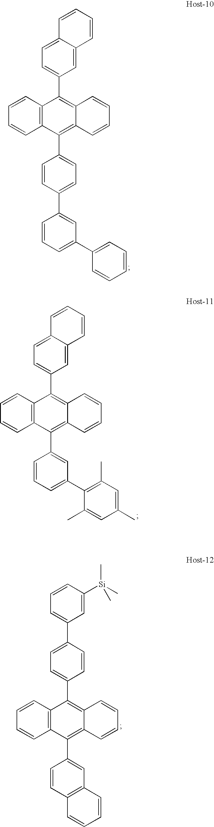
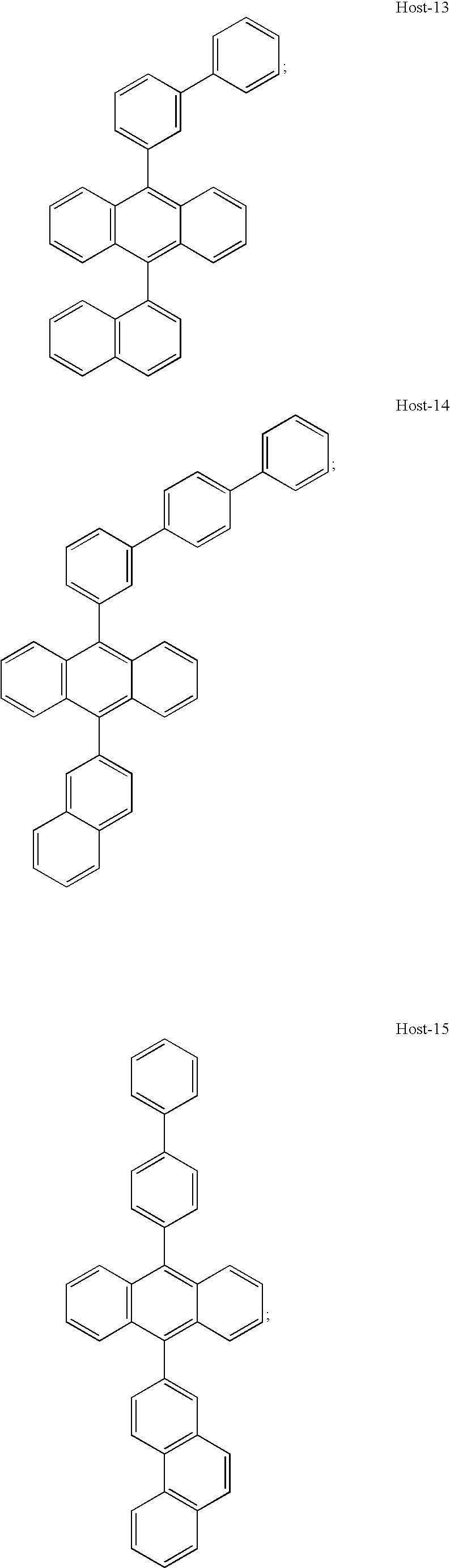


wherein:
-
- A and A′ represent independent azine ring systems corresponding to 6-membered aromatic ring systems containing at least one nitrogen;
- (Xa)n and (Xb)m represent one or more independently selected substituents and include acyclic substituents or are joined to form a ring fused to A or A′;
- m and n are independently 0 to 4;
- Za and Zb are independently selected substituents;
- 1, 2, 3, 4, 1′, 2′, 3′, and 4′ are independently selected as either carbon or nitrogen atoms; and
- provided that Xa, Xb, Za, and Zb, 1, 2, 3, 4, 1′, 2′, 3′, and 4′ are selected to provide blue luminescence.

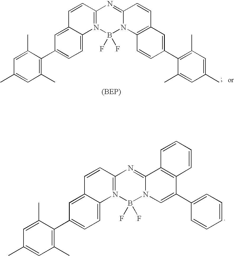

and bis[2-[4-[N,N-diarylamino]phenyl]vinyl]biphenyls of the general structure N2 shown below:


wherein R1 through R4 can be the same or different and individually represent hydrogen or one or more substituents, for example, alkyl groups, such as methyl groups, alkoxy groups, such as methoxy, aryl groups, such as phenyl, or aryloxy groups, such as phenoxy.


wherein substituent groups R1 and R2 are independently alkyl, alkoxyl, aryl, or heteroaryl; and substituent groups R3 through R12 are independently hydrogen, alkyl, alkoxyl, halogen, aryl, or heteroaryl, and adjacent substituent groups R3 through R10 can optionally be connected to form one or more ring systems, including fused aromatic and fused heteroaromatic rings, between 510 nm and 540 nm, and a full width at half maximum of 40 nm or less. Alkyl, alkoxyl, aryl, heteroaryl, fused aromatic ring and fused heteroaromatic ring substituent groups are further substituted. Conveniently, R1 and R2 are aryl, and R2 through R12 are hydrogen, or substituent groups that are more electron withdrawing than methyl. Some examples of useful quinacridones include those disclosed in U.S. Pat. No. 5,593,788 and in U.S. Patent Publication 2004/0001969 A1.
Examples of useful quinacridone green dopants include:

The green light-emitting materials can include a coumarin compound of the following structure:

wherein:
-
- X is O or S, R1, R2, R3 and R6 can individually be hydrogen, alkyl, or aryl;
- R4 and R5 can individually be alkyl or aryl, or where either R3 and R4; or
- R5 and R6, or both together represent the atoms completing a cycloalkyl group.
Examples of useful coumarin green dopants include:


wherein:
-
- M represents a metal;
- n is an integer of from 1 to 3; and
- Z independently in each occurrence represents the atoms completing a nucleus having at least two fused aromatic rings.
-
- CO-1: Aluminum trisoxine [alias, tris(8-quinolinolato)aluminum(III)];
- CO-2: Magnesium bisoxine [alias, bis(8-quinolinolato)magnesium(II)];
- CO-3: Bis[benzo {f}-8-quinolinolato]zinc (II);
- CO-4: Bis(2-methyl-8-quinolinolato)aluminum(III)-μ-oxo-bis(2-methyl-8-quinolinolato) aluminum(III);
- CO-5: Indium trisoxine [alias, tris(8-quinolinolato)indium];
- CO-6: Aluminum tris(5-methyloxine) [alias, tris(5-methyl-8-quinolinolato) aluminum(III)];
- CO-7: Lithium oxine [alias, (8-quinolinolato)lithium(I)];
- CO-8: Gallium oxine [alias, tris(8-quinolinolato)gallium(III)]; and
- CO-9: Zirconium oxine [alias, tetra(8-quinolinolato)zirconium(IV)].
| 10 | | ||
| 11a | |
||
| 11b | |
||
| 11c | |
||
| 11d | pixel | ||
| 12 | |
||
| 14 | |
||
| 100 | |
||
| 110a | |
||
| 110b | |
||
| 110c | |
||
| 110d | |
||
| 122 | hole-transporting |
||
| 123a | magenta |
||
| 123c | green |
||
| 124 | electron-transporting |
||
| 130 | |
||
| 140a | |
||
| | color filter | ||
| | color filter | ||
| 160 | |
||
| 162 | |
||
| 170 | relative |
||
| 172 | |
||
| 174 | |
||
| 210a | external |
||
| 210b | external |
||
| 210c | external |
||
| 210d | external |
||
| 220a | internal |
||
| 220b | internal |
||
| 220c | internal |
||
| 220d | internal light emission | ||
Claims (12)
Priority Applications (14)
| Application Number | Priority Date | Filing Date | Title |
|---|---|---|---|
| US11/315,827 US7602119B2 (en) | 2005-04-25 | 2005-12-22 | OLED with magenta and green emissive layers |
| DE602006011296T DE602006011296D1 (en) | 2005-04-25 | 2006-04-19 | MULTI COLOR OLED INDICATORS |
| DE602006014815T DE602006014815D1 (en) | 2005-04-25 | 2006-04-19 | MULTI COLOR OLED INDICATORS |
| EP06758429A EP1875505B1 (en) | 2005-04-25 | 2006-04-19 | Oled multicolor displays |
| PCT/US2006/015539 WO2006116347A2 (en) | 2005-04-25 | 2006-04-19 | Multicolor oled displays |
| JP2008508929A JP5350781B2 (en) | 2005-04-25 | 2006-04-19 | Multi-color OLED display |
| EP06751300A EP1875509B1 (en) | 2005-04-25 | 2006-04-19 | Multicolor oled displays |
| PCT/US2006/014822 WO2006115960A1 (en) | 2005-04-25 | 2006-04-19 | Oled multicolor displays |
| DE602006018442T DE602006018442D1 (en) | 2005-04-25 | 2006-04-19 | MULTI COLOR OLED INDICATORS |
| PCT/US2006/015538 WO2006116346A2 (en) | 2005-04-25 | 2006-04-19 | Multicolor oled displays |
| JP2008509019A JP2008539556A (en) | 2005-04-25 | 2006-04-19 | Multi-color OLED display |
| EP06751301A EP1875510B1 (en) | 2005-04-25 | 2006-04-19 | Multicolor oled displays |
| JP2008509018A JP5558708B2 (en) | 2005-04-25 | 2006-04-19 | Multi-color OLED display |
| JP2012156174A JP5457512B2 (en) | 2005-04-25 | 2012-07-12 | Multi-color OLED display |
Applications Claiming Priority (3)
| Application Number | Priority Date | Filing Date | Title |
|---|---|---|---|
| US11/113,484 US7471041B2 (en) | 2005-04-25 | 2005-04-25 | OLED multicolor displays |
| US11/113,915 US7436113B2 (en) | 2005-04-25 | 2005-04-25 | Multicolor OLED displays |
| US11/315,827 US7602119B2 (en) | 2005-04-25 | 2005-12-22 | OLED with magenta and green emissive layers |
Related Parent Applications (1)
| Application Number | Title | Priority Date | Filing Date |
|---|---|---|---|
| US11/113,484 Continuation-In-Part US7471041B2 (en) | 2005-04-25 | 2005-04-25 | OLED multicolor displays |
Publications (2)
| Publication Number | Publication Date |
|---|---|
| US20060238120A1 US20060238120A1 (en) | 2006-10-26 |
| US7602119B2 true US7602119B2 (en) | 2009-10-13 |
Family
ID=36793420
Family Applications (1)
| Application Number | Title | Priority Date | Filing Date |
|---|---|---|---|
| US11/315,827 Active 2027-03-26 US7602119B2 (en) | 2005-04-25 | 2005-12-22 | OLED with magenta and green emissive layers |
Country Status (5)
| Country | Link |
|---|---|
| US (1) | US7602119B2 (en) |
| EP (3) | EP1875510B1 (en) |
| JP (4) | JP2008539556A (en) |
| DE (3) | DE602006018442D1 (en) |
| WO (3) | WO2006116347A2 (en) |
Cited By (5)
| Publication number | Priority date | Publication date | Assignee | Title |
|---|---|---|---|---|
| US20100171910A1 (en) * | 2009-01-08 | 2010-07-08 | Yun-I Liu | Display Device and Display Panel and Color Filter thereof |
| US20130120981A1 (en) * | 2011-11-15 | 2013-05-16 | Lg Display Co., Ltd. | Organic Light Emitting Display Panel and Method of Manufacturing the Same |
| US20140320385A1 (en) * | 2013-04-24 | 2014-10-30 | Samsung Display Co., Ltd. | Organic light emitting diode display |
| US9741967B2 (en) | 2011-03-25 | 2017-08-22 | Semiconductor Energy Laboratory Co., Ltd. | Light-emitting panel having plurality of organic light-emitting elements |
| US9893303B2 (en) | 2013-03-27 | 2018-02-13 | Semiconductor Energy Laboratory Co., Ltd. | Light-emitting element, light-emitting device, electronic appliance, and lighting device |
Families Citing this family (52)
| Publication number | Priority date | Publication date | Assignee | Title |
|---|---|---|---|---|
| KR101189154B1 (en) * | 2006-06-08 | 2012-11-09 | 삼성디스플레이 주식회사 | Organic Light Emitting Display Device |
| US20080157659A1 (en) * | 2006-12-28 | 2008-07-03 | Shiva Prakash | Electronic device including an organic device layer |
| JP4479737B2 (en) * | 2007-03-07 | 2010-06-09 | セイコーエプソン株式会社 | LIGHT EMITTING DEVICE, ITS MANUFACTURING METHOD, AND ELECTRONIC DEVICE |
| JP4529988B2 (en) | 2007-03-08 | 2010-08-25 | セイコーエプソン株式会社 | Light emitting device and electronic device |
| US8183767B2 (en) * | 2007-07-06 | 2012-05-22 | Canon Kabushiki Kaisha | Display apparatus and imaging system using the same |
| JP2009037886A (en) * | 2007-08-02 | 2009-02-19 | Seiko Epson Corp | Organic electroluminescent device |
| KR20090063469A (en) * | 2007-12-14 | 2009-06-18 | 삼성전자주식회사 | Orgarnic transistor display substrate, method of manufacturing the same, and display apparatus having the same |
| WO2009116628A1 (en) | 2008-03-19 | 2009-09-24 | 出光興産株式会社 | Anthracene derivatives, luminescent materials and organic electroluminescent devices |
| US8053770B2 (en) * | 2008-10-14 | 2011-11-08 | Universal Display Corporation | Emissive layer patterning for OLED |
| CN102474937A (en) * | 2009-07-06 | 2012-05-23 | 先锋股份有限公司 | Display device and method for manufacturing the same |
| US8877356B2 (en) * | 2009-07-22 | 2014-11-04 | Global Oled Technology Llc | OLED device with stabilized yellow light-emitting layer |
| DE102009042680A1 (en) * | 2009-09-23 | 2011-03-24 | Merck Patent Gmbh | Organic electroluminescent device |
| JP5609058B2 (en) * | 2009-10-22 | 2014-10-22 | ソニー株式会社 | Display device |
| KR101125570B1 (en) * | 2009-12-04 | 2012-03-22 | 삼성모바일디스플레이주식회사 | Organic light emitting diode device |
| JP5431280B2 (en) * | 2010-09-24 | 2014-03-05 | 株式会社東芝 | Organic EL display |
| JP2012204164A (en) * | 2011-03-25 | 2012-10-22 | Sony Corp | Organic el display device and method for manufacturing the same |
| JP5837316B2 (en) * | 2011-03-25 | 2015-12-24 | 株式会社Joled | Organic EL display device and manufacturing method thereof |
| JP2013012477A (en) | 2011-06-28 | 2013-01-17 | Cbrite Inc | Hybrid full-color active matrix organic light emitting display |
| JP5927601B2 (en) * | 2011-09-07 | 2016-06-01 | 株式会社Joled | Luminescent panel, display device and electronic device |
| KR101931770B1 (en) * | 2011-11-30 | 2018-12-24 | 삼성디스플레이 주식회사 | Mask assembly and organic light emitting diode display |
| TWI508279B (en) | 2012-01-19 | 2015-11-11 | Joled Inc | Display and method of manufacturing the same, unit, transfer printing method, organic electroluminescence unit and method of manufacturing the same, and electronic apparatus |
| JP6031649B2 (en) * | 2012-01-19 | 2016-11-24 | 株式会社Joled | Organic electroluminescent device, organic electroluminescent device manufacturing method, and electronic apparatus |
| JP2012156136A (en) * | 2012-03-09 | 2012-08-16 | Sony Corp | Organic light emitting display device |
| KR102022698B1 (en) | 2012-05-31 | 2019-11-05 | 삼성디스플레이 주식회사 | Display panel |
| KR101954973B1 (en) * | 2012-09-19 | 2019-03-08 | 삼성디스플레이 주식회사 | Organic light emitting display |
| WO2014069492A1 (en) * | 2012-10-30 | 2014-05-08 | Semiconductor Energy Laboratory Co., Ltd. | Light-emitting panel, display device, and method for manufacturing light-emitting panel |
| KR101990312B1 (en) | 2012-12-31 | 2019-06-18 | 엘지디스플레이 주식회사 | Organic Light Emitting Diode Display Device and Method for Manufacturing The Same |
| US10229956B2 (en) * | 2013-01-18 | 2019-03-12 | Universal Display Corporation | High resolution low power consumption OLED display with extended lifetime |
| US9385168B2 (en) * | 2013-01-18 | 2016-07-05 | Universal Display Corporation | High resolution low power consumption OLED display with extended lifetime |
| US10580832B2 (en) | 2013-01-18 | 2020-03-03 | Universal Display Corporation | High resolution low power consumption OLED display with extended lifetime |
| US9590017B2 (en) | 2013-01-18 | 2017-03-07 | Universal Display Corporation | High resolution low power consumption OLED display with extended lifetime |
| US10304906B2 (en) | 2013-01-18 | 2019-05-28 | Universal Display Corporation | High resolution low power consumption OLED display with extended lifetime |
| US10243023B2 (en) | 2013-01-18 | 2019-03-26 | Universal Display Corporation | Top emission AMOLED displays using two emissive layers |
| JP5849981B2 (en) * | 2013-03-25 | 2016-02-03 | ソニー株式会社 | Display device and electronic device |
| KR20150014007A (en) * | 2013-07-25 | 2015-02-06 | 삼성전자주식회사 | Image sensor and imaging device including the same |
| JP2015069758A (en) * | 2013-09-27 | 2015-04-13 | 株式会社ジャパンディスプレイ | Organic el display device |
| TWI515891B (en) | 2013-11-01 | 2016-01-01 | 友達光電股份有限公司 | Display panel |
| JP2015138612A (en) * | 2014-01-21 | 2015-07-30 | 株式会社ジャパンディスプレイ | Organic electroluminescence display device |
| JP6656817B2 (en) * | 2014-04-25 | 2020-03-04 | 株式会社半導体エネルギー研究所 | Light emitting device |
| US10700134B2 (en) | 2014-05-27 | 2020-06-30 | Universal Display Corporation | Low power consumption OLED display |
| CN106489207A (en) * | 2014-05-27 | 2017-03-08 | 环球展览公司 | Have and prolong long-life high-resolution low power consumption OLED display |
| KR102305143B1 (en) | 2014-08-20 | 2021-09-28 | 삼성디스플레이 주식회사 | Display device and manufacturing method thereof |
| WO2016052152A1 (en) * | 2014-10-01 | 2016-04-07 | ソニー株式会社 | Display device and electronic apparatus |
| US9818804B2 (en) | 2015-09-18 | 2017-11-14 | Universal Display Corporation | Hybrid display |
| US10263050B2 (en) | 2015-09-18 | 2019-04-16 | Universal Display Corporation | Hybrid display |
| US10777613B2 (en) * | 2016-04-14 | 2020-09-15 | Sharp Kabushiki Kaisha | Display device and manufacturing method therefor |
| CN106373989B (en) * | 2016-11-24 | 2019-10-22 | 上海天马有机发光显示技术有限公司 | A kind of organic light emitting display panel, electronic equipment and production method |
| CN107068886B (en) * | 2017-05-12 | 2019-01-25 | 京东方科技集团股份有限公司 | Organic electroluminescence device and preparation method thereof, light emitting device |
| KR20190033816A (en) * | 2017-09-22 | 2019-04-01 | 삼성전자주식회사 | Display panel and display apparatus |
| US10797112B2 (en) | 2018-07-25 | 2020-10-06 | Universal Display Corporation | Energy efficient OLED TV |
| KR20210005345A (en) * | 2019-07-03 | 2021-01-14 | 한국전자통신연구원 | Display device and manufacturing method thereof |
| CN116762478A (en) * | 2021-02-12 | 2023-09-15 | 索尼半导体解决方案公司 | Display device and electronic device |
Citations (17)
| Publication number | Priority date | Publication date | Assignee | Title |
|---|---|---|---|---|
| US4800375A (en) | 1986-10-24 | 1989-01-24 | Honeywell Inc. | Four color repetitive sequence matrix array for flat panel displays |
| US5113274A (en) | 1988-06-13 | 1992-05-12 | Mitsubishi Denki Kabushiki Kaisha | Matrix-type color liquid crystal display device |
| US5276380A (en) | 1991-12-30 | 1994-01-04 | Eastman Kodak Company | Organic electroluminescent image display device |
| US5550066A (en) | 1994-12-14 | 1996-08-27 | Eastman Kodak Company | Method of fabricating a TFT-EL pixel |
| US20010043043A1 (en) | 2000-01-07 | 2001-11-22 | Megumi Aoyama | Organic electroluminescent display panel and organic electroluminescent device used therefor |
| US20020186214A1 (en) | 2001-06-05 | 2002-12-12 | Eastman Kodak Company | Method for saving power in an organic electroluminescent display using white light emitting elements |
| US20020191130A1 (en) | 2001-06-19 | 2002-12-19 | Wei-Chen Liang | Color display utilizing combinations of four colors |
| US6570584B1 (en) | 2000-05-15 | 2003-05-27 | Eastman Kodak Company | Broad color gamut display |
| US20030170491A1 (en) | 2002-02-15 | 2003-09-11 | Eastman Kodak Company | Providing an organic electroluminescent device having stacked electroluminescent units |
| US6693611B1 (en) | 1998-08-19 | 2004-02-17 | Cambridge Display Technology Ltd. | Display devices |
| US20050045917A1 (en) | 2001-12-28 | 2005-03-03 | Semiconductor Energy Laboratory Co., Ltd. | Light emitting device, method of manufacturing the same and manufacturing apparatus therefor |
| KR20050031888A (en) | 2003-09-30 | 2005-04-06 | 산요덴키가부시키가이샤 | Electroluminesence display device |
| US20050073230A1 (en) | 2003-09-30 | 2005-04-07 | Ryuji Nishikawa | Organic EL element and organic EL panel |
| US20050116615A1 (en) | 2003-09-30 | 2005-06-02 | Shoichiro Matsumoto | Light emissive display device |
| US7142179B2 (en) * | 2005-03-23 | 2006-11-28 | Eastman Kodak Company | OLED display device |
| US7436113B2 (en) * | 2005-04-25 | 2008-10-14 | Eastman Kodak Company | Multicolor OLED displays |
| US7439670B2 (en) * | 2005-02-03 | 2008-10-21 | Eastman Kodak Company | Making multicolor OLED displays |
Family Cites Families (15)
| Publication number | Priority date | Publication date | Assignee | Title |
|---|---|---|---|---|
| JPH0992465A (en) * | 1995-09-22 | 1997-04-04 | Fuji Electric Co Ltd | Electroluminescent element |
| JPH09274991A (en) * | 1996-04-08 | 1997-10-21 | Fuji Electric Co Ltd | Multi-color light emission electroluminescence device |
| JPH1012379A (en) * | 1996-06-24 | 1998-01-16 | Idemitsu Kosan Co Ltd | Multicolor light emission device and its manufacture |
| JPH11354273A (en) * | 1998-06-09 | 1999-12-24 | Idemitsu Kosan Co Ltd | Multicolor light emitting device |
| JP2002175879A (en) * | 2000-12-08 | 2002-06-21 | Tdk Corp | Organic el display panel and organic el element using the same |
| JP4644938B2 (en) * | 2001-01-15 | 2011-03-09 | ソニー株式会社 | Organic electroluminescence device |
| JP4069745B2 (en) * | 2002-12-26 | 2008-04-02 | 株式会社デンソー | Organic EL panel |
| JP2004296136A (en) * | 2003-03-25 | 2004-10-21 | Tdk Corp | Laminated thin film el element and manufacturing method thereof, and el panel |
| KR100490322B1 (en) * | 2003-04-07 | 2005-05-17 | 삼성전자주식회사 | Organic electro-luminescent display |
| US6919681B2 (en) * | 2003-04-30 | 2005-07-19 | Eastman Kodak Company | Color OLED display with improved power efficiency |
| US6771028B1 (en) * | 2003-04-30 | 2004-08-03 | Eastman Kodak Company | Drive circuitry for four-color organic light-emitting device |
| JP4895490B2 (en) * | 2003-09-30 | 2012-03-14 | 三洋電機株式会社 | Organic EL panel |
| JP4731865B2 (en) * | 2003-10-03 | 2011-07-27 | 株式会社半導体エネルギー研究所 | Light emitting device |
| TWI296181B (en) * | 2005-08-01 | 2008-04-21 | Univision Technology Inc | Full color organic electroluminescent display device with low power consumption |
| TWI283549B (en) * | 2005-09-30 | 2007-07-01 | Univision Technology Inc | Organic electroluminescent display device with improved color saturation and method of fabricating the same |
-
2005
- 2005-12-22 US US11/315,827 patent/US7602119B2/en active Active
-
2006
- 2006-04-19 WO PCT/US2006/015539 patent/WO2006116347A2/en active Application Filing
- 2006-04-19 WO PCT/US2006/015538 patent/WO2006116346A2/en active Application Filing
- 2006-04-19 EP EP06751301A patent/EP1875510B1/en active Active
- 2006-04-19 JP JP2008509019A patent/JP2008539556A/en not_active Withdrawn
- 2006-04-19 EP EP06751300A patent/EP1875509B1/en active Active
- 2006-04-19 EP EP06758429A patent/EP1875505B1/en active Active
- 2006-04-19 JP JP2008509018A patent/JP5558708B2/en active Active
- 2006-04-19 DE DE602006018442T patent/DE602006018442D1/en active Active
- 2006-04-19 DE DE602006011296T patent/DE602006011296D1/en active Active
- 2006-04-19 DE DE602006014815T patent/DE602006014815D1/en active Active
- 2006-04-19 WO PCT/US2006/014822 patent/WO2006115960A1/en active Application Filing
- 2006-04-19 JP JP2008508929A patent/JP5350781B2/en active Active
-
2012
- 2012-07-12 JP JP2012156174A patent/JP5457512B2/en active Active
Patent Citations (18)
| Publication number | Priority date | Publication date | Assignee | Title |
|---|---|---|---|---|
| US4800375A (en) | 1986-10-24 | 1989-01-24 | Honeywell Inc. | Four color repetitive sequence matrix array for flat panel displays |
| US5113274A (en) | 1988-06-13 | 1992-05-12 | Mitsubishi Denki Kabushiki Kaisha | Matrix-type color liquid crystal display device |
| US5276380A (en) | 1991-12-30 | 1994-01-04 | Eastman Kodak Company | Organic electroluminescent image display device |
| US5550066A (en) | 1994-12-14 | 1996-08-27 | Eastman Kodak Company | Method of fabricating a TFT-EL pixel |
| US6693611B1 (en) | 1998-08-19 | 2004-02-17 | Cambridge Display Technology Ltd. | Display devices |
| US20010043043A1 (en) | 2000-01-07 | 2001-11-22 | Megumi Aoyama | Organic electroluminescent display panel and organic electroluminescent device used therefor |
| US6570584B1 (en) | 2000-05-15 | 2003-05-27 | Eastman Kodak Company | Broad color gamut display |
| US20020186214A1 (en) | 2001-06-05 | 2002-12-12 | Eastman Kodak Company | Method for saving power in an organic electroluminescent display using white light emitting elements |
| US20020191130A1 (en) | 2001-06-19 | 2002-12-19 | Wei-Chen Liang | Color display utilizing combinations of four colors |
| US20050045917A1 (en) | 2001-12-28 | 2005-03-03 | Semiconductor Energy Laboratory Co., Ltd. | Light emitting device, method of manufacturing the same and manufacturing apparatus therefor |
| US20030170491A1 (en) | 2002-02-15 | 2003-09-11 | Eastman Kodak Company | Providing an organic electroluminescent device having stacked electroluminescent units |
| US6872472B2 (en) * | 2002-02-15 | 2005-03-29 | Eastman Kodak Company | Providing an organic electroluminescent device having stacked electroluminescent units |
| KR20050031888A (en) | 2003-09-30 | 2005-04-06 | 산요덴키가부시키가이샤 | Electroluminesence display device |
| US20050073230A1 (en) | 2003-09-30 | 2005-04-07 | Ryuji Nishikawa | Organic EL element and organic EL panel |
| US20050116615A1 (en) | 2003-09-30 | 2005-06-02 | Shoichiro Matsumoto | Light emissive display device |
| US7439670B2 (en) * | 2005-02-03 | 2008-10-21 | Eastman Kodak Company | Making multicolor OLED displays |
| US7142179B2 (en) * | 2005-03-23 | 2006-11-28 | Eastman Kodak Company | OLED display device |
| US7436113B2 (en) * | 2005-04-25 | 2008-10-14 | Eastman Kodak Company | Multicolor OLED displays |
Non-Patent Citations (1)
| Title |
|---|
| S. Tasch et al., The Application of Poly(Phenylene) Type Polymers and Oligomers in Electroluminescent Color Displays, Materials Research Society Symposium Proceedings, Materials Research Society, Pittsburg, PA, US, vol. 471, 1997, pp. 325-330, XP000979688. |
Cited By (11)
| Publication number | Priority date | Publication date | Assignee | Title |
|---|---|---|---|---|
| US20100171910A1 (en) * | 2009-01-08 | 2010-07-08 | Yun-I Liu | Display Device and Display Panel and Color Filter thereof |
| US8054419B2 (en) * | 2009-01-08 | 2011-11-08 | Au Optronics Corp. | Display device and display panel and color filter thereof |
| US9741967B2 (en) | 2011-03-25 | 2017-08-22 | Semiconductor Energy Laboratory Co., Ltd. | Light-emitting panel having plurality of organic light-emitting elements |
| US10333106B2 (en) | 2011-03-25 | 2019-06-25 | Semiconductor Energy Laboratory Co., Ltd. | Light-emitting panel having plurality of organic light-emitting elements |
| US20130120981A1 (en) * | 2011-11-15 | 2013-05-16 | Lg Display Co., Ltd. | Organic Light Emitting Display Panel and Method of Manufacturing the Same |
| US9062852B2 (en) * | 2011-11-15 | 2015-06-23 | Lg Display Co., Ltd. | Organic light emitting display panel and method of manufacturing the same |
| US9653520B2 (en) | 2011-11-15 | 2017-05-16 | Lg Display Co., Ltd. | Organic light emitting display panel and method of manufacturing the same |
| US9893303B2 (en) | 2013-03-27 | 2018-02-13 | Semiconductor Energy Laboratory Co., Ltd. | Light-emitting element, light-emitting device, electronic appliance, and lighting device |
| US11723264B2 (en) | 2013-03-27 | 2023-08-08 | Semiconductor Energy Laboratory Co., Ltd. | Light-emitting element, light-emitting device, electronic appliance, and lighting device |
| US20140320385A1 (en) * | 2013-04-24 | 2014-10-30 | Samsung Display Co., Ltd. | Organic light emitting diode display |
| US9721499B2 (en) * | 2013-04-24 | 2017-08-01 | Samsung Display Co., Ltd. | Organic light emitting diode display including driving voltage line |
Also Published As
| Publication number | Publication date |
|---|---|
| WO2006116346A2 (en) | 2006-11-02 |
| EP1875510A2 (en) | 2008-01-09 |
| EP1875505B1 (en) | 2010-11-24 |
| EP1875505A1 (en) | 2008-01-09 |
| DE602006018442D1 (en) | 2011-01-05 |
| JP2008539555A (en) | 2008-11-13 |
| JP5558708B2 (en) | 2014-07-23 |
| WO2006116346A3 (en) | 2006-12-14 |
| DE602006014815D1 (en) | 2010-07-22 |
| JP5457512B2 (en) | 2014-04-02 |
| WO2006115960A1 (en) | 2006-11-02 |
| US20060238120A1 (en) | 2006-10-26 |
| WO2006116347A2 (en) | 2006-11-02 |
| EP1875509B1 (en) | 2010-06-09 |
| JP2008539556A (en) | 2008-11-13 |
| WO2006116347A3 (en) | 2006-12-14 |
| EP1875510B1 (en) | 2009-12-23 |
| JP5350781B2 (en) | 2013-11-27 |
| DE602006011296D1 (en) | 2010-02-04 |
| JP2012195310A (en) | 2012-10-11 |
| EP1875509A2 (en) | 2008-01-09 |
| JP2008539554A (en) | 2008-11-13 |
Similar Documents
| Publication | Publication Date | Title |
|---|---|---|
| US7602119B2 (en) | OLED with magenta and green emissive layers | |
| US7471041B2 (en) | OLED multicolor displays | |
| US7436113B2 (en) | Multicolor OLED displays | |
| US7439670B2 (en) | Making multicolor OLED displays | |
| JP5421432B2 (en) | Anthracene derivative host containing various dopants | |
| EP1449904B1 (en) | White-emitting organic electroluminescent device with color filters to improve efficiency | |
| US7247394B2 (en) | Tuned microcavity color OLED display | |
| US7192659B2 (en) | OLED device using reduced drive voltage | |
| US7023013B2 (en) | Array of light-emitting OLED microcavity pixels | |
| US8179035B2 (en) | Selecting white point for OLED devices | |
| US7288330B2 (en) | High performance white light-emitting OLED device | |
| US20050147844A1 (en) | White oled devices with color filter arrays |
Legal Events
| Date | Code | Title | Description |
|---|---|---|---|
| AS | Assignment |
Owner name: EASTMAN KODAK COMPANY, NEW YORK Free format text: ASSIGNMENT OF ASSIGNORS INTEREST;ASSIGNORS:MILLER, MICHAEL E.;SPINDLER, JEFFREY P.;REEL/FRAME:017408/0956;SIGNING DATES FROM 20051220 TO 20051221 |
|
| STCF | Information on status: patent grant |
Free format text: PATENTED CASE |
|
| FEPP | Fee payment procedure |
Free format text: PAYOR NUMBER ASSIGNED (ORIGINAL EVENT CODE: ASPN); ENTITY STATUS OF PATENT OWNER: LARGE ENTITY |
|
| CC | Certificate of correction | ||
| AS | Assignment |
Owner name: GLOBAL OLED TECHNOLOGY LLC,DELAWARE Free format text: ASSIGNMENT OF ASSIGNORS INTEREST;ASSIGNOR:EASTMAN KODAK COMPANY;REEL/FRAME:023998/0368 Effective date: 20100122 Owner name: GLOBAL OLED TECHNOLOGY LLC, DELAWARE Free format text: ASSIGNMENT OF ASSIGNORS INTEREST;ASSIGNOR:EASTMAN KODAK COMPANY;REEL/FRAME:023998/0368 Effective date: 20100122 |
|
| FPAY | Fee payment |
Year of fee payment: 4 |
|
| FPAY | Fee payment |
Year of fee payment: 8 |
|
| MAFP | Maintenance fee payment |
Free format text: PAYMENT OF MAINTENANCE FEE, 12TH YEAR, LARGE ENTITY (ORIGINAL EVENT CODE: M1553); ENTITY STATUS OF PATENT OWNER: LARGE ENTITY Year of fee payment: 12 |