US7602201B2 - High temperature ceramic socket configured to test packaged semiconductor devices - Google Patents
High temperature ceramic socket configured to test packaged semiconductor devices Download PDFInfo
- Publication number
- US7602201B2 US7602201B2 US11/766,938 US76693807A US7602201B2 US 7602201 B2 US7602201 B2 US 7602201B2 US 76693807 A US76693807 A US 76693807A US 7602201 B2 US7602201 B2 US 7602201B2
- Authority
- US
- United States
- Prior art keywords
- socket
- single piece
- piece socket
- holes
- test
- Prior art date
- Legal status (The legal status is an assumption and is not a legal conclusion. Google has not performed a legal analysis and makes no representation as to the accuracy of the status listed.)
- Active, expires
Links
Images


Classifications
-
- G—PHYSICS
- G01—MEASURING; TESTING
- G01R—MEASURING ELECTRIC VARIABLES; MEASURING MAGNETIC VARIABLES
- G01R1/00—Details of instruments or arrangements of the types included in groups G01R5/00 - G01R13/00 and G01R31/00
- G01R1/02—General constructional details
- G01R1/04—Housings; Supporting members; Arrangements of terminals
- G01R1/0408—Test fixtures or contact fields; Connectors or connecting adaptors; Test clips; Test sockets
- G01R1/0433—Sockets for IC's or transistors
Definitions
- the invention relates generally to sockets to receive packaged integrated circuits for test purposes and, more particularly, to a test socket to receive leads of a semiconductor package such as a dual in-line semiconductor package, or DIP.
- test sockets are provided to receive and protect the leads of the IC during the test.
- test sockets are mounted on a printed circuit board (PCB) with a PCB providing interconnections between the ICs and test equipment.
- PCB printed circuit board
- a conventional test socket is shown in an exploded view in FIG. 1 .
- Pins 10 having holes for receiving the IC leads are housed between a bottom plate 12 and a top plate 14 .
- the diameter of each pin 10 is smaller at the bottom for reception in a hole 16 through bottom plate 12 with a recessed larger portion hole being configured to receive a flange on the upper end of each pin 10 .
- top plate 14 is assembled to bottom plate 12 by suitable fasteners such as screws (not shown) to retain the pins in the bottom plate 12 .
- Top plate 14 has holes 18 extending therethrough in alignment with pins 10 and configured to receive leads of an IC package. However, holes 18 are smaller in diameter than the flanges of pins 10 whereby the pins 10 are captured between the top plate 14 and the bottom plate 12 .
- FIG. 2 illustrates a socket, such as the FIG. 1 socket, attached to a printed circuit board (PCB) 40 .
- PCB printed circuit board
- the pins 10 of the sockets are aligned with the conductive pads 34 on the PCB.
- Several screws 38 are provided through the PCB 40 and into the bottom plate 12 and top plate 14 via a holder plate 30 .
- the leads 48 of the IC 50 may be inserted into the holes 18 to achieve the electrical connection to the pads 34 via the pins 10 and springs 36 .
- the socket is made from a conductive material coated with a non-conductive material.
- the coating of non-conductive material is to prevent shorting from one IC lead 48 to another IC lead 48 .
- a test socket assembly is for use in testing integrated circuits.
- a single piece socket is formed substantially of an insulating material and having a plurality of holes formed therein configured to receive a plurality of electrically conductive springs. Each hole of the single piece socket has therein a separate one of the electrically conductive springs.
- a test socket includes a plurality of pins configured to receive leads of an integrated circuit, the pins of the test socket extending into the plurality of holes of the single piece socket with each pin engaging a spring, wherein the single piece socket is positioned on a circuit board with the plurality of holes being in alignment with electrical contacts on the circuit board such that the plurality of springs are electrically interconnecting the contacts and the plurality of pins.
- the single-piece socket is comprised substantially of a high-temperature insulating material, such as ceramic.
- FIG. 1 is an exploded view of a conventional test socket.
- FIG. 2 is a side view in section of the FIG. 1 conventional test socket in a configuration attached to a printed circuit board for testing an integrated circuit.
- FIG. 3 is a side view in section of an improved socket assembly.
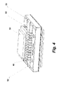
- FIG. 4 illustrates a perspective view of the FIG. 3 socket assembly.
- the inventors have realized that, with extensive use and, further, due to manufacturing limitations of the socket, the non-conductive material of test sockets such as described in the Background disintegrates, resulting in inadvertent shorts between one IC lead and another.
- the inventors have further realized that assembly of the three-plate structure, that holds the pins and springs, can be time consuming.
- the socket is formed of a non-conductive material such as ceramic.
- a one-piece socket is provided, which makes the socket assembly more manufacturable (with a decrease in both cost of parts and labor), and also provides improved reliability and performance.
- the socket 46 has holes 32 aligned with contact pads 34 on the PCB.
- Positioned in holes 32 are pins 10 and helical springs 36 formed, for example, of a very thin, gold plated, high temperature spring wire.
- the springs 36 have a diameter similar to the pins 10 but slightly smaller than the base of the pins to ensure contact with the socket pins, and holes 32 in the socket are slightly larger than the socket pins for reception of the pin in engagement with springs 36 . Both pins 10 and springs 36 are held in place inside the holes 32 in the body of socket 46 .
- Socket 46 is secured to PCB 40 using several screws 41 , or other suitable fasteners, which travels through socket 46 , through PCB 40 , and held in place into a steel nut-plate 43 .
- a thin insulating material 42 is between PCB 40 and nut-plate 43 to minimize the chance of the nut-plate electrically shorting to PCB 40 circuit conductors or causing mechanical abrasions to PCB 40 .
- socket assembly In use of the socket assembly, leads 48 of the integrated circuit 50 (only a portion shown) are received in holes 32 of the socket assembly, and physically engage the pins 10 which are electrically connected to pads 34 via the springs 36 being compressed.
- the sockets are “non-ZIF,” meaning that non-zero insertion force is required to insert and/or remove the packaged test devices into the sockets, such as by using a commercially available tool to insert and remove the packaged test devices using a certain amount of physical force.
- the socket assembly may allow for placement of, for example, single packaged devices with up to 28 pins in 300 or 600 mil widths, as well as two smaller packages up to 14 pins each in either 300 or 600 mil widths, placed in a serial end-to-end or back-to-back configuration.
- the 600 mil packages may also be placed in a side-by-side parallel configuration of two 14-pin packed integrated circuits end-to-end, as well as side-by-side. These are just examples, and many other configurations may be possible.
- FIG. 4 illustrates a perspective view of the FIG. 3 socket assembly, including leads 48 of the integrated circuit 50 received in holes 32 of the socket assembly. From this perspective view, the three rows of holes 32 are visible.
- the FIG. 4 perspective view also shows steps 52 at the ends of the socket. The steps 52 at the two ends and blank holes on those steps are features that allow, for example, for longer packages to be tested without the user having to trim package pins.
- conventional IC removal tools such as a flat screwdriver, may be used against the step surface to remove test packages.
- the socket of the socket assembly is integrally formed of a single piece, thus enhancing the manufacturability.
- the probability of a short being caused by the socket is minimized (e.g., as a result of a thin coating of insulating material being disintegrated).
Abstract
Description
Claims (11)
Priority Applications (7)
| Application Number | Priority Date | Filing Date | Title |
|---|---|---|---|
| US11/766,938 US7602201B2 (en) | 2007-06-22 | 2007-06-22 | High temperature ceramic socket configured to test packaged semiconductor devices |
| JP2010513293A JP2010530973A (en) | 2007-06-22 | 2008-05-16 | High temperature ceramic socket configured to test packaged semiconductor devices |
| CN2008800214874A CN101690422B (en) | 2007-06-22 | 2008-05-16 | High temperature ceramic socket configured to test packaged semiconductor devices |
| PCT/US2008/063902 WO2009002630A1 (en) | 2007-06-22 | 2008-05-16 | High temperature ceramic socket configured to test packaged semiconductor devices |
| TW097119384A TWI427294B (en) | 2007-06-22 | 2008-05-26 | High temperature ceramic socket configured to test packaged semiconductor devices |
| JP2015001448A JP2015092503A (en) | 2007-06-22 | 2015-01-07 | High temperature ceramic socket configured to test packaged semiconductor device |
| JP2016143056A JP6478949B2 (en) | 2007-06-22 | 2016-07-21 | High temperature ceramic socket configured to test packaged semiconductor devices |
Applications Claiming Priority (1)
| Application Number | Priority Date | Filing Date | Title |
|---|---|---|---|
| US11/766,938 US7602201B2 (en) | 2007-06-22 | 2007-06-22 | High temperature ceramic socket configured to test packaged semiconductor devices |
Publications (2)
| Publication Number | Publication Date |
|---|---|
| US20080315900A1 US20080315900A1 (en) | 2008-12-25 |
| US7602201B2 true US7602201B2 (en) | 2009-10-13 |
Family
ID=40135837
Family Applications (1)
| Application Number | Title | Priority Date | Filing Date |
|---|---|---|---|
| US11/766,938 Active 2027-07-13 US7602201B2 (en) | 2007-06-22 | 2007-06-22 | High temperature ceramic socket configured to test packaged semiconductor devices |
Country Status (5)
| Country | Link |
|---|---|
| US (1) | US7602201B2 (en) |
| JP (3) | JP2010530973A (en) |
| CN (1) | CN101690422B (en) |
| TW (1) | TWI427294B (en) |
| WO (1) | WO2009002630A1 (en) |
Cited By (7)
| Publication number | Priority date | Publication date | Assignee | Title |
|---|---|---|---|---|
| US20080168849A1 (en) * | 2007-01-12 | 2008-07-17 | Shenzhen Futaihong Precision Industry Co., Ltd. | Testing devices for multihole workpiece |
| US20100112827A1 (en) * | 2008-11-03 | 2010-05-06 | Hon Hai Precision Industry Co., Ltd. | Board mounted electrical connector with reinforcing device |
| US20100271041A1 (en) * | 2009-04-27 | 2010-10-28 | Yung-Yu Wu | Testing apparatus with high efficiency and high accuracy |
| US20140366350A1 (en) * | 2011-12-28 | 2014-12-18 | C/O Showa Denko K.K. | Jig for manufacturing capacitor element and method for manufacturing capacitor element |
| US9196428B2 (en) | 2010-12-13 | 2015-11-24 | Showa Denko K.K. | Gang socket and jig for manufacturing capacitor element that uses said gang socket |
| US20160084905A1 (en) * | 2014-09-24 | 2016-03-24 | Micron Technology, Inc. | Apparatus for testing stacked die assemblies, and related methods |
| US11163004B2 (en) * | 2016-12-16 | 2021-11-02 | Technoprobe S.P.A. | Probe head for a testing apparatus of electronic devices with enhanced filtering properties |
Families Citing this family (4)
| Publication number | Priority date | Publication date | Assignee | Title |
|---|---|---|---|---|
| KR101204941B1 (en) * | 2012-04-27 | 2012-11-27 | 주식회사 아이에스시 | Socket for test with electrode supporting member and fabrication method thereof |
| KR101370409B1 (en) * | 2012-12-05 | 2014-03-07 | 에이케이이노텍주식회사 | Semiconductor test socket |
| CN106252954B (en) * | 2016-09-27 | 2018-07-20 | 浙江宏泰锆业科技有限公司 | A kind of mobile phone and the ceramic skeleton of electric appliance charging or connection plug |
| CN108647172B (en) * | 2018-06-04 | 2020-04-10 | 北京航天时代光电科技有限公司 | Program burning method of EEPROM chip |
Citations (18)
| Publication number | Priority date | Publication date | Assignee | Title |
|---|---|---|---|---|
| US4326765A (en) * | 1980-04-15 | 1982-04-27 | International Telephone And Telegraph Corporation | Electronic device carrier |
| US5038467A (en) | 1989-11-09 | 1991-08-13 | Advanced Interconnections Corporation | Apparatus and method for installation of multi-pin components on circuit boards |
| US5199889A (en) | 1991-11-12 | 1993-04-06 | Jem Tech | Leadless grid array socket |
| US5399108A (en) * | 1993-09-08 | 1995-03-21 | Tongrand Limited | LIF PGA socket and contact therein and method making the same |
| US5479105A (en) * | 1993-06-25 | 1995-12-26 | Samsung Electronics Co., Ltd. | Known-good die testing apparatus |
| US5519331A (en) | 1994-11-10 | 1996-05-21 | Lsi Logic Corporation | Removable biasing board for automated testing of integrated circuits |
| US5523586A (en) * | 1993-09-20 | 1996-06-04 | Kabushiki Kaisha Toshiba | Burn-in socket used in a burn-in test for semiconductor chips |
| US5534787A (en) | 1994-12-09 | 1996-07-09 | Vlsi Technology, Inc. | High-frequency coaxial interface test fixture |
| US5568057A (en) * | 1993-05-14 | 1996-10-22 | Samsung Electronics Co., Ltd. | Method for performing a burn-in test |
| US6208155B1 (en) | 1998-01-27 | 2001-03-27 | Cerprobe Corporation | Probe tip and method for making electrical contact with a solder ball contact of an integrated circuit device |
| US6278283B1 (en) | 1998-05-11 | 2001-08-21 | Mitsubishi Denki Kabushiki Kaisha | Capacitance detecting circuit |
| US6667628B2 (en) | 2002-04-02 | 2003-12-23 | Agilent Technologies, Inc. | Method and apparatus for the management of forces in a wireless fixture |
| US20040140821A1 (en) * | 2003-01-21 | 2004-07-22 | Chaeyoon Lee | Test PCB and contactor for testing of electronic device |
| US6798228B2 (en) * | 2003-01-10 | 2004-09-28 | Qualitau, Inc. | Test socket for packaged semiconductor devices |
| US6821131B2 (en) | 2002-10-28 | 2004-11-23 | Yamaichi Electronics Co., Ltd. | IC socket for a fine pitch IC package |
| US6958616B1 (en) * | 2003-11-07 | 2005-10-25 | Xilinx, Inc. | Hybrid interface apparatus for testing integrated circuits having both low-speed and high-speed input/output pins |
| US20050280428A1 (en) * | 2004-02-27 | 2005-12-22 | Takaji Ishikawa | Probe card and the production method |
| US7172450B1 (en) | 2006-01-11 | 2007-02-06 | Qualitau, Inc. | High temperature open ended zero insertion force (ZIF) test socket |
Family Cites Families (14)
| Publication number | Priority date | Publication date | Assignee | Title |
|---|---|---|---|---|
| JPS628478A (en) * | 1985-07-03 | 1987-01-16 | 東洋通信機株式会社 | Socket for piezo-electric resonator |
| JPS6237894U (en) * | 1985-08-27 | 1987-03-06 | ||
| JPH0337985A (en) * | 1989-07-04 | 1991-02-19 | Hitachi Ltd | Multipolar connector |
| JPH05203672A (en) * | 1992-01-24 | 1993-08-10 | Sony Corp | Method and device for measuring electronic component |
| JPH06260568A (en) * | 1993-03-09 | 1994-09-16 | Nippon Steel Corp | Ic socket |
| JP3653131B2 (en) * | 1995-12-28 | 2005-05-25 | 日本発条株式会社 | Conductive contact |
| JPH11233216A (en) * | 1998-02-16 | 1999-08-27 | Nippon Denki Factory Engineering Kk | Ic socket for test |
| CN1129214C (en) * | 1999-11-17 | 2003-11-26 | 株式会社爱德万测试 | IC socket and IC tester |
| JP2002042922A (en) * | 2000-07-21 | 2002-02-08 | Shin Etsu Polymer Co Ltd | Electric connector and its manufacturing method |
| JP3443687B2 (en) * | 2001-02-19 | 2003-09-08 | 株式会社エンプラス | Socket for electrical components |
| JP3526291B2 (en) * | 2001-04-25 | 2004-05-10 | 三菱電機株式会社 | Capacitor module and semiconductor device using the same |
| EP1400811B1 (en) * | 2001-06-28 | 2015-09-30 | NHK SPRING Co., Ltd. | Support body assembly for conductive contactor |
| JP4775554B2 (en) * | 2003-07-10 | 2011-09-21 | 日本電気株式会社 | LSI test socket for BGA |
| CN2859845Y (en) * | 2005-10-14 | 2007-01-17 | 北京工业大学 | Safety stand for DIP programmable chip programme debugging |
-
2007
- 2007-06-22 US US11/766,938 patent/US7602201B2/en active Active
-
2008
- 2008-05-16 CN CN2008800214874A patent/CN101690422B/en active Active
- 2008-05-16 WO PCT/US2008/063902 patent/WO2009002630A1/en active Application Filing
- 2008-05-16 JP JP2010513293A patent/JP2010530973A/en active Pending
- 2008-05-26 TW TW097119384A patent/TWI427294B/en active
-
2015
- 2015-01-07 JP JP2015001448A patent/JP2015092503A/en active Pending
-
2016
- 2016-07-21 JP JP2016143056A patent/JP6478949B2/en active Active
Patent Citations (18)
| Publication number | Priority date | Publication date | Assignee | Title |
|---|---|---|---|---|
| US4326765A (en) * | 1980-04-15 | 1982-04-27 | International Telephone And Telegraph Corporation | Electronic device carrier |
| US5038467A (en) | 1989-11-09 | 1991-08-13 | Advanced Interconnections Corporation | Apparatus and method for installation of multi-pin components on circuit boards |
| US5199889A (en) | 1991-11-12 | 1993-04-06 | Jem Tech | Leadless grid array socket |
| US5568057A (en) * | 1993-05-14 | 1996-10-22 | Samsung Electronics Co., Ltd. | Method for performing a burn-in test |
| US5479105A (en) * | 1993-06-25 | 1995-12-26 | Samsung Electronics Co., Ltd. | Known-good die testing apparatus |
| US5399108A (en) * | 1993-09-08 | 1995-03-21 | Tongrand Limited | LIF PGA socket and contact therein and method making the same |
| US5523586A (en) * | 1993-09-20 | 1996-06-04 | Kabushiki Kaisha Toshiba | Burn-in socket used in a burn-in test for semiconductor chips |
| US5519331A (en) | 1994-11-10 | 1996-05-21 | Lsi Logic Corporation | Removable biasing board for automated testing of integrated circuits |
| US5534787A (en) | 1994-12-09 | 1996-07-09 | Vlsi Technology, Inc. | High-frequency coaxial interface test fixture |
| US6208155B1 (en) | 1998-01-27 | 2001-03-27 | Cerprobe Corporation | Probe tip and method for making electrical contact with a solder ball contact of an integrated circuit device |
| US6278283B1 (en) | 1998-05-11 | 2001-08-21 | Mitsubishi Denki Kabushiki Kaisha | Capacitance detecting circuit |
| US6667628B2 (en) | 2002-04-02 | 2003-12-23 | Agilent Technologies, Inc. | Method and apparatus for the management of forces in a wireless fixture |
| US6821131B2 (en) | 2002-10-28 | 2004-11-23 | Yamaichi Electronics Co., Ltd. | IC socket for a fine pitch IC package |
| US6798228B2 (en) * | 2003-01-10 | 2004-09-28 | Qualitau, Inc. | Test socket for packaged semiconductor devices |
| US20040140821A1 (en) * | 2003-01-21 | 2004-07-22 | Chaeyoon Lee | Test PCB and contactor for testing of electronic device |
| US6958616B1 (en) * | 2003-11-07 | 2005-10-25 | Xilinx, Inc. | Hybrid interface apparatus for testing integrated circuits having both low-speed and high-speed input/output pins |
| US20050280428A1 (en) * | 2004-02-27 | 2005-12-22 | Takaji Ishikawa | Probe card and the production method |
| US7172450B1 (en) | 2006-01-11 | 2007-02-06 | Qualitau, Inc. | High temperature open ended zero insertion force (ZIF) test socket |
Non-Patent Citations (2)
| Title |
|---|
| International Search Report from Corresponding PCT Application No. PCT/US08/63902 dated Aug. 19, 2008. |
| Written Opinion from Corresponding PCT Application No. PCT/US08/63902 dated Aug. 19, 2008. |
Cited By (16)
| Publication number | Priority date | Publication date | Assignee | Title |
|---|---|---|---|---|
| US7798022B2 (en) * | 2007-01-12 | 2010-09-21 | Shenzhen Futaihong Precision Industry Co., Ltd. | Testing devices for multihole workpiece |
| US20080168849A1 (en) * | 2007-01-12 | 2008-07-17 | Shenzhen Futaihong Precision Industry Co., Ltd. | Testing devices for multihole workpiece |
| US20100112827A1 (en) * | 2008-11-03 | 2010-05-06 | Hon Hai Precision Industry Co., Ltd. | Board mounted electrical connector with reinforcing device |
| US7938648B2 (en) * | 2008-11-03 | 2011-05-10 | Hon Hai Precision Ind. Co., Ltd. | Board mounted electrical connector with reinforcing device |
| US20100271041A1 (en) * | 2009-04-27 | 2010-10-28 | Yung-Yu Wu | Testing apparatus with high efficiency and high accuracy |
| US8044675B2 (en) * | 2009-04-27 | 2011-10-25 | Princeton Technology Corporation | Testing apparatus with high efficiency and high accuracy |
| US9196428B2 (en) | 2010-12-13 | 2015-11-24 | Showa Denko K.K. | Gang socket and jig for manufacturing capacitor element that uses said gang socket |
| US9251954B2 (en) * | 2011-12-28 | 2016-02-02 | Showa Denko K.K. | Jig for manufacturing capacitor element and method for manufacturing capacitor element |
| US20140366350A1 (en) * | 2011-12-28 | 2014-12-18 | C/O Showa Denko K.K. | Jig for manufacturing capacitor element and method for manufacturing capacitor element |
| US20160084905A1 (en) * | 2014-09-24 | 2016-03-24 | Micron Technology, Inc. | Apparatus for testing stacked die assemblies, and related methods |
| US9733304B2 (en) * | 2014-09-24 | 2017-08-15 | Micron Technology, Inc. | Semiconductor device test apparatuses |
| US20170336470A1 (en) * | 2014-09-24 | 2017-11-23 | Micron Technology, Inc. | Methods of testing semiconductor devices |
| US10126357B2 (en) * | 2014-09-24 | 2018-11-13 | Micron Technology, Inc. | Methods of testing semiconductor devices comprising a die stack having protruding conductive elements |
| US20190072608A1 (en) * | 2014-09-24 | 2019-03-07 | Micron Technology, Inc. | Semiconductor device test apparatuses |
| US10481200B2 (en) * | 2014-09-24 | 2019-11-19 | Micron Technology, Inc. | Semiconductor device test apparatuses comprising at least one test site having an array of pockets |
| US11163004B2 (en) * | 2016-12-16 | 2021-11-02 | Technoprobe S.P.A. | Probe head for a testing apparatus of electronic devices with enhanced filtering properties |
Also Published As
| Publication number | Publication date |
|---|---|
| JP2010530973A (en) | 2010-09-16 |
| JP6478949B2 (en) | 2019-03-06 |
| US20080315900A1 (en) | 2008-12-25 |
| TWI427294B (en) | 2014-02-21 |
| JP2015092503A (en) | 2015-05-14 |
| CN101690422A (en) | 2010-03-31 |
| WO2009002630A1 (en) | 2008-12-31 |
| CN101690422B (en) | 2011-11-16 |
| TW200916785A (en) | 2009-04-16 |
| JP2016197120A (en) | 2016-11-24 |
Similar Documents
| Publication | Publication Date | Title |
|---|---|---|
| US7602201B2 (en) | High temperature ceramic socket configured to test packaged semiconductor devices | |
| US5629837A (en) | Button contact for surface mounting an IC device to a circuit board | |
| US6407566B1 (en) | Test module for multi-chip module simulation testing of integrated circuit packages | |
| US6222379B1 (en) | Conventionally sized temporary package for testing semiconductor dice | |
| US6392429B1 (en) | Temporary semiconductor package having dense array external contacts | |
| US7255576B2 (en) | Kelvin contact module for a microcircuit test system | |
| US6798228B2 (en) | Test socket for packaged semiconductor devices | |
| WO2006028633A2 (en) | Hermaphroditic socket/adapter | |
| US20080018353A1 (en) | Methods and apparatus for releasably mounting a semiconductor device to a printed circuit board | |
| US20110143559A1 (en) | Socket and Contact Having Anchors | |
| US6974335B1 (en) | Interchangeable multi-form factor module socket | |
| KR101957961B1 (en) | Socket board assembly | |
| US6285202B1 (en) | Test carrier with force applying mechanism guide and terminal contact protector | |
| US7242203B2 (en) | Probe retention kit, and system and method for probing a pattern of points on a printed circuit board | |
| JP2734412B2 (en) | Semiconductor device socket | |
| US20100134998A1 (en) | Adapter, socket, electronic device, and mounting method | |
| KR20170119452A (en) | Insert assembly for receiving semiconductor device and test tray including the same | |
| US6459286B2 (en) | Test head assembly utilizing replaceable silicon contact | |
| KR20110125186A (en) | Test socket for testing performance a semiconductor chip package | |
| US6888158B2 (en) | Bare chip carrier and method for manufacturing semiconductor device using the bare chip carrier | |
| KR20110125185A (en) | Signal detection pin for test socket for testing performance a semiconductor chip package | |
| KR100844486B1 (en) | Test socket for semiconductor chip | |
| US20060267620A1 (en) | Interconnecting apparatus and a contact element therefor | |
| KR20140021890A (en) | Prove module for electrical inspection and method of manufaturing the same | |
| KR100621180B1 (en) | Connector for pcb |
Legal Events
| Date | Code | Title | Description |
|---|---|---|---|
| AS | Assignment |
Owner name: QUALITAU, INC., CALIFORNIA Free format text: ASSIGNMENT OF ASSIGNORS INTEREST;ASSIGNORS:YSAGUIRRE, JOSE;ULLMANN, JENS;RAMIREZ, ADALBERTO M.;AND OTHERS;REEL/FRAME:019468/0811 Effective date: 20070621 |
|
| STCF | Information on status: patent grant |
Free format text: PATENTED CASE |
|
| FPAY | Fee payment |
Year of fee payment: 4 |
|
| FPAY | Fee payment |
Year of fee payment: 8 |
|
| MAFP | Maintenance fee payment |
Free format text: PAYMENT OF MAINTENANCE FEE, 12TH YR, SMALL ENTITY (ORIGINAL EVENT CODE: M2553); ENTITY STATUS OF PATENT OWNER: SMALL ENTITY Year of fee payment: 12 |