US7602366B2 - Liquid crystal display device - Google Patents
Liquid crystal display device Download PDFInfo
- Publication number
- US7602366B2 US7602366B2 US11/006,642 US664204A US7602366B2 US 7602366 B2 US7602366 B2 US 7602366B2 US 664204 A US664204 A US 664204A US 7602366 B2 US7602366 B2 US 7602366B2
- Authority
- US
- United States
- Prior art keywords
- liquid crystal
- crystal display
- display panel
- drive circuit
- common voltage
- Prior art date
- Legal status (The legal status is an assumption and is not a legal conclusion. Google has not performed a legal analysis and makes no representation as to the accuracy of the status listed.)
- Expired - Fee Related, expires
Links
Images


Classifications
-
- G—PHYSICS
- G09—EDUCATION; CRYPTOGRAPHY; DISPLAY; ADVERTISING; SEALS
- G09G—ARRANGEMENTS OR CIRCUITS FOR CONTROL OF INDICATING DEVICES USING STATIC MEANS TO PRESENT VARIABLE INFORMATION
- G09G3/00—Control arrangements or circuits, of interest only in connection with visual indicators other than cathode-ray tubes
- G09G3/20—Control arrangements or circuits, of interest only in connection with visual indicators other than cathode-ray tubes for presentation of an assembly of a number of characters, e.g. a page, by composing the assembly by combination of individual elements arranged in a matrix no fixed position being assigned to or needed to be assigned to the individual characters or partial characters
- G09G3/34—Control arrangements or circuits, of interest only in connection with visual indicators other than cathode-ray tubes for presentation of an assembly of a number of characters, e.g. a page, by composing the assembly by combination of individual elements arranged in a matrix no fixed position being assigned to or needed to be assigned to the individual characters or partial characters by control of light from an independent source
- G09G3/36—Control arrangements or circuits, of interest only in connection with visual indicators other than cathode-ray tubes for presentation of an assembly of a number of characters, e.g. a page, by composing the assembly by combination of individual elements arranged in a matrix no fixed position being assigned to or needed to be assigned to the individual characters or partial characters by control of light from an independent source using liquid crystals
- G09G3/3611—Control of matrices with row and column drivers
- G09G3/3685—Details of drivers for data electrodes
- G09G3/3688—Details of drivers for data electrodes suitable for active matrices only
-
- G—PHYSICS
- G09—EDUCATION; CRYPTOGRAPHY; DISPLAY; ADVERTISING; SEALS
- G09G—ARRANGEMENTS OR CIRCUITS FOR CONTROL OF INDICATING DEVICES USING STATIC MEANS TO PRESENT VARIABLE INFORMATION
- G09G3/00—Control arrangements or circuits, of interest only in connection with visual indicators other than cathode-ray tubes
- G09G3/20—Control arrangements or circuits, of interest only in connection with visual indicators other than cathode-ray tubes for presentation of an assembly of a number of characters, e.g. a page, by composing the assembly by combination of individual elements arranged in a matrix no fixed position being assigned to or needed to be assigned to the individual characters or partial characters
- G09G3/34—Control arrangements or circuits, of interest only in connection with visual indicators other than cathode-ray tubes for presentation of an assembly of a number of characters, e.g. a page, by composing the assembly by combination of individual elements arranged in a matrix no fixed position being assigned to or needed to be assigned to the individual characters or partial characters by control of light from an independent source
- G09G3/36—Control arrangements or circuits, of interest only in connection with visual indicators other than cathode-ray tubes for presentation of an assembly of a number of characters, e.g. a page, by composing the assembly by combination of individual elements arranged in a matrix no fixed position being assigned to or needed to be assigned to the individual characters or partial characters by control of light from an independent source using liquid crystals
- G09G3/3611—Control of matrices with row and column drivers
- G09G3/3648—Control of matrices with row and column drivers using an active matrix
- G09G3/3655—Details of drivers for counter electrodes, e.g. common electrodes for pixel capacitors or supplementary storage capacitors
-
- G—PHYSICS
- G06—COMPUTING; CALCULATING OR COUNTING
- G06F—ELECTRIC DIGITAL DATA PROCESSING
- G06F3/00—Input arrangements for transferring data to be processed into a form capable of being handled by the computer; Output arrangements for transferring data from processing unit to output unit, e.g. interface arrangements
- G06F3/14—Digital output to display device ; Cooperation and interconnection of the display device with other functional units
- G06F3/1423—Digital output to display device ; Cooperation and interconnection of the display device with other functional units controlling a plurality of local displays, e.g. CRT and flat panel display
-
- G—PHYSICS
- G09—EDUCATION; CRYPTOGRAPHY; DISPLAY; ADVERTISING; SEALS
- G09G—ARRANGEMENTS OR CIRCUITS FOR CONTROL OF INDICATING DEVICES USING STATIC MEANS TO PRESENT VARIABLE INFORMATION
- G09G2310/00—Command of the display device
- G09G2310/02—Addressing, scanning or driving the display screen or processing steps related thereto
- G09G2310/0264—Details of driving circuits
- G09G2310/0281—Arrangement of scan or data electrode driver circuits at the periphery of a panel not inherent to a split matrix structure
-
- G—PHYSICS
- G09—EDUCATION; CRYPTOGRAPHY; DISPLAY; ADVERTISING; SEALS
- G09G—ARRANGEMENTS OR CIRCUITS FOR CONTROL OF INDICATING DEVICES USING STATIC MEANS TO PRESENT VARIABLE INFORMATION
- G09G2320/00—Control of display operating conditions
- G09G2320/02—Improving the quality of display appearance
- G09G2320/0209—Crosstalk reduction, i.e. to reduce direct or indirect influences of signals directed to a certain pixel of the displayed image on other pixels of said image, inclusive of influences affecting pixels in different frames or fields or sub-images which constitute a same image, e.g. left and right images of a stereoscopic display
- G09G2320/0214—Crosstalk reduction, i.e. to reduce direct or indirect influences of signals directed to a certain pixel of the displayed image on other pixels of said image, inclusive of influences affecting pixels in different frames or fields or sub-images which constitute a same image, e.g. left and right images of a stereoscopic display with crosstalk due to leakage current of pixel switch in active matrix panels
-
- G—PHYSICS
- G09—EDUCATION; CRYPTOGRAPHY; DISPLAY; ADVERTISING; SEALS
- G09G—ARRANGEMENTS OR CIRCUITS FOR CONTROL OF INDICATING DEVICES USING STATIC MEANS TO PRESENT VARIABLE INFORMATION
- G09G2320/00—Control of display operating conditions
- G09G2320/08—Arrangements within a display terminal for setting, manually or automatically, display parameters of the display terminal
-
- G—PHYSICS
- G09—EDUCATION; CRYPTOGRAPHY; DISPLAY; ADVERTISING; SEALS
- G09G—ARRANGEMENTS OR CIRCUITS FOR CONTROL OF INDICATING DEVICES USING STATIC MEANS TO PRESENT VARIABLE INFORMATION
- G09G2330/00—Aspects of power supply; Aspects of display protection and defect management
- G09G2330/02—Details of power systems and of start or stop of display operation
- G09G2330/021—Power management, e.g. power saving
-
- G—PHYSICS
- G09—EDUCATION; CRYPTOGRAPHY; DISPLAY; ADVERTISING; SEALS
- G09G—ARRANGEMENTS OR CIRCUITS FOR CONTROL OF INDICATING DEVICES USING STATIC MEANS TO PRESENT VARIABLE INFORMATION
- G09G2360/00—Aspects of the architecture of display systems
- G09G2360/18—Use of a frame buffer in a display terminal, inclusive of the display panel
-
- G—PHYSICS
- G09—EDUCATION; CRYPTOGRAPHY; DISPLAY; ADVERTISING; SEALS
- G09G—ARRANGEMENTS OR CIRCUITS FOR CONTROL OF INDICATING DEVICES USING STATIC MEANS TO PRESENT VARIABLE INFORMATION
- G09G3/00—Control arrangements or circuits, of interest only in connection with visual indicators other than cathode-ray tubes
- G09G3/20—Control arrangements or circuits, of interest only in connection with visual indicators other than cathode-ray tubes for presentation of an assembly of a number of characters, e.g. a page, by composing the assembly by combination of individual elements arranged in a matrix no fixed position being assigned to or needed to be assigned to the individual characters or partial characters
- G09G3/34—Control arrangements or circuits, of interest only in connection with visual indicators other than cathode-ray tubes for presentation of an assembly of a number of characters, e.g. a page, by composing the assembly by combination of individual elements arranged in a matrix no fixed position being assigned to or needed to be assigned to the individual characters or partial characters by control of light from an independent source
- G09G3/36—Control arrangements or circuits, of interest only in connection with visual indicators other than cathode-ray tubes for presentation of an assembly of a number of characters, e.g. a page, by composing the assembly by combination of individual elements arranged in a matrix no fixed position being assigned to or needed to be assigned to the individual characters or partial characters by control of light from an independent source using liquid crystals
- G09G3/3611—Control of matrices with row and column drivers
- G09G3/3614—Control of polarity reversal in general
-
- G—PHYSICS
- G09—EDUCATION; CRYPTOGRAPHY; DISPLAY; ADVERTISING; SEALS
- G09G—ARRANGEMENTS OR CIRCUITS FOR CONTROL OF INDICATING DEVICES USING STATIC MEANS TO PRESENT VARIABLE INFORMATION
- G09G3/00—Control arrangements or circuits, of interest only in connection with visual indicators other than cathode-ray tubes
- G09G3/20—Control arrangements or circuits, of interest only in connection with visual indicators other than cathode-ray tubes for presentation of an assembly of a number of characters, e.g. a page, by composing the assembly by combination of individual elements arranged in a matrix no fixed position being assigned to or needed to be assigned to the individual characters or partial characters
- G09G3/34—Control arrangements or circuits, of interest only in connection with visual indicators other than cathode-ray tubes for presentation of an assembly of a number of characters, e.g. a page, by composing the assembly by combination of individual elements arranged in a matrix no fixed position being assigned to or needed to be assigned to the individual characters or partial characters by control of light from an independent source
- G09G3/36—Control arrangements or circuits, of interest only in connection with visual indicators other than cathode-ray tubes for presentation of an assembly of a number of characters, e.g. a page, by composing the assembly by combination of individual elements arranged in a matrix no fixed position being assigned to or needed to be assigned to the individual characters or partial characters by control of light from an independent source using liquid crystals
- G09G3/3611—Control of matrices with row and column drivers
- G09G3/3696—Generation of voltages supplied to electrode drivers
Definitions
- the present invention relates in general to a liquid crystal display device, and, more particularly, the invention relates to a technique which is effective when applied to a drive circuit of a liquid crystal display device having two liquid crystal display panels, which is used in a mobile phone or the like.
- a liquid crystal display module adopting a TFT (Thin Film Transistor) method which has a miniaturized liquid crystal display panel for color display having a sub pixel number of approximately 100 ⁇ 150 ⁇ 3, or an organic EL display device having an organic EL element, has been popularly used as a display part of a PDA (Personal Digital Assist), a mobile phone and the like. Further, recently, a foldable mobile phone which includes a main display part and a sub display part has been available.
- TFT Thin Film Transistor
- the first liquid crystal display panel and the second liquid crystal display panel are connected with each other using connection lines formed on a flexible printed circuit board, and, at the same time, the first and second liquid crystal display panels are driven by one liquid crystal drive circuit.
- the liquid crystal display module described in the above-mentioned patent document 1, assuming that the number of display lines of the main display part is s “m” and the number of display lines of the sub display part is “n”, the liquid crystal display module is driven as a single screen having pseudo (m+n) display lines; and, hence, it is impossible to adopt driving methods which are optimum to the main display part and the sub display part, respectively, whereby a reduction of the power consumption is hampered.
- the present invention has been made to overcome the above-mentioned drawback, and it is an object of the present invention to provide a technique which can ensure a low power consumption by realizing an optimum driving method in a miniaturized liquid crystal display device having two liquid crystal display panels.
- the present invention is directed to a liquid crystal display device which includes a first liquid crystal display panel; a second liquid crystal display panel; a drive circuit which is mounted on the first liquid crystal display panel; output terminals which are mounted on the first liquid crystal display panel and to which signals outputted from the drive circuit are supplied; and connection lines which connect the output terminals and the second liquid crystal display panel.
- the drive circuit is capable of changing the AC driving method employed during a display period of the first liquid crystal display panel and the AC driving method employed during a display period of the second liquid crystal display panel, which are present within the same frame.
- the present invention is also characterized in that the alternating of the first common voltage is stopped during a non-display period of the first liquid crystal display panel, and the alternating of the second common voltage is stopped during a non-display period of the second liquid crystal display panel.
- the present invention is also characterized in that the drive circuit includes a booster circuit part and the booster circuit part is capable of changing the operational mode thereof in response to an external signal.
- the present invention is also characterized in that the drive circuit includes a gray scale voltage generating part, and the drive circuit stops the operation of unnecessary amplifying circuits in the inside of the gray scale voltage generating part during a non-display period of the first liquid crystal display panel or the second liquid crystal display panel.
- FIG. 1 is a schematic diagram showing the constitution of a liquid crystal display module representing an embodiment 1 of the present invention
- FIG. 2 is a schematic diagram showing the constitution of a liquid crystal display module representing a modification of the embodiment 1 of the present invention
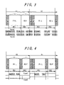
- FIG. 3 is a diagram showing an AC driving method of a conventional liquid crystal display module
- FIG. 4 is a diagram showing one example of the AC driving method of the liquid crystal display module of the embodiment 1 of the present invention.
- FIG. 5 is a table showing instruction signals used in the liquid crystal display module of the embodiment 1 of the present invention.
- FIG. 6 is a diagram showing signals transferred from a first drive circuit to a second drive circuit when the drive circuit is divided in two in the liquid crystal display module of the embodiment 1 of the present invention
- FIG. 7 is a diagram showing signals transferred from a first drive circuit to a second drive circuit when the drive circuit is divided in two in the liquid crystal display module of the embodiment 1 of the present invention
- FIG. 8A is a diagram showing one example of an AC driving method of a liquid crystal display module representing an embodiment 2 of the present invention
- FIG. 8B and FIG. 8C are schematic circuit diagrams of circuits used to implement the method
- FIG. 9A is a diagram showing another example of the AC driving method of the liquid crystal display module of the embodiment 2 of the present invention
- FIG. 9B and FIG. 9C are schematic circuit diagrams of circuits used to implement the method
- FIG. 10A is a diagram showing another example of the AC driving method of the liquid crystal display module of the embodiment 2 of the present invention
- FIGS. 10B and FIG. 10C are schematic circuit diagrams of circuits used to implement the method
- FIG. 11 is a block diagram showing the constitution of one example of a source driver SD of the liquid crystal display module of the embodiment 1 of the present invention.
- FIG. 12 is a block diagram showing one example of the constitution of a gray scale voltage generating circuit and a selector in a liquid crystal display module representing an embodiment 3 of the present invention
- FIG. 13 is a block diagram showing another example of the constitution of the gray scale voltage generating circuit and the selector in a liquid crystal display module of the embodiment 3 of the present invention.
- FIG. 14A is a schematic circuit diagram of a booster circuit of a liquid crystal display module representing an embodiment 4 of the present invention.
- FIG. 14B is a schematic circuit diagram of a booster circuit of a liquid crystal display module representing an embodiment 4 of the present invention.
- FIG. 14C is a schematic circuit diagram of the booster circuit of a liquid crystal display module of the embodiment 4 of the present invention.
- FIG. 15 is a schematic circuit diagram showing the more specific constitution of the booster circuit shown in FIGS. 14A to 14C .
- FIG. 1 is a schematic diagram showing the constitution of a liquid crystal display module representing this embodiment 1.
- the liquid crystal display module of this embodiment is an integral type liquid crystal display module, which includes a first liquid crystal display panel and a second liquid crystal display panel.
- PNL 1 indicates the first liquid crystal display panel, which constitutes a main display part when a foldable mobile phone is used in an opened state
- PNL 2 indicates the second liquid crystal display panel, which constitutes a sub display part when a foldable mobile phone is used in a closed state.
- a plurality of scanning lines (or gate lines) GL and a plurality of video lines (or drain lines) SL are respectively arranged in parallel. Pixel portions are formed at portions where the scanning lines GL and the video lines SL intersect each other. A plurality of pixel portions are arranged in a matrix array, and each pixel portion is provided with a pixel electrode 12 and a thin film transistor 10 .
- the first and second liquid crystal display panels PNL 1 , PNL 2 are configured such that glass substrates SUB 1 , SUB 2 on which the pixel electrodes 12 , the thin film transistors 10 and the like are formed, and a glass substrate (not shown in the drawing) on which color filter and the like are formed, are overlapped relative to each other with a given gap therebetween. Both substrates are laminated to each other using a sealing material formed in a frame shape in the vicinity of peripheral portions between both substrates, and further, liquid crystal is filled and sealed in the inside of the space defined by the sealing material, which is disposed between both substrates, through a liquid crystal sealing opening formed in a portion of the sealing material. Further, polarizers are laminated to the outside of both substrates.
- the present invention is not relevant to the inner structure of the liquid crystal display panel, a detailed explanation of the inner structure of the liquid crystal display panel is omitted. Further, the present invention is applicable to a liquid crystal display panel having any structure.
- a first drive circuit DRV 1 is mounted on the glass substrate SUB 1 of the first liquid crystal display panel PNL 1 .
- the first drive circuit DRV 1 includes a controller CNTL, a source driver SD which drives the video lines SL of the first and second liquid crystal display panels PNL 1 , PNL 2 , a gate driver GD which drives the scanning lines GL of the first and second liquid crystal display panels PNL 1 , PNL 2 , a power source circuit PC which supplies a first common voltage Vcom 1 to a common electrode (also referred to as a counter electrode) 15 of the first liquid crystal display panel PNL 1 and a second common voltage Vcom 2 to a common electrode (also referred to as a counter electrode) 15 of the second liquid crystal display panel PNL 2 and the like.
- a source driver SD which drives the video lines SL of the first and second liquid crystal display panels PNL 1 , PNL 2
- a gate driver GD which drives the scanning lines GL of the first and second liquid crystal display panels PNL 1 , PNL 2
- a power source circuit PC which supplies a first common voltage Vcom 1 to a common electrode (also referred to as a counter electrode) 15 of the first liquid
- a MPU Microcomputer Unit
- FIG. 1 shows a case in which the first drive circuit DRV 1 is constituted of one semiconductor chip.
- FIG. 2 is a block diagram showing the schematic constitution of a modification of a liquid crystal display module of this embodiment.
- the liquid crystal display module shown in FIG. 2 is characterized by dividing the drive circuit into two circuits, that is, a first drive circuit DRV 1 and a second drive circuit DRV 2 .
- the first drive circuit DRV 1 includes a controller CNTL and a source driver SD which drives the video lines SL of the first and second liquid crystal display panels PNL 1 , PNL 2 ; while, the second drive circuit DRV 2 includes the gate driver GD which drives the scanning lines GL of the first and second liquid crystal display panels PNL 1 , PNL 2 and a power source circuit PC which supplies the first common voltage Vcom 1 to the common electrode 15 of the first liquid crystal display panel PNL 1 and the second common voltage Vcom 2 to the common electrode 15 of the second liquid crystal display panel PNL 2 . Further, the first drive circuit DRV 1 and the second drive circuit DRV 2 are respectively constituted of one semiconductor chip.
- terminals are formed on the first liquid crystal display panel PNL 1 and the second liquid crystal display panel PNL 2 and these terminals are connected with a flexible printed wiring board FPC, whereby the second liquid crystal display panel PNL 2 is connected with the first liquid crystal display panel PNL 1 by way of the flexible printed wiring board FPC.
- connection lines for video lines, connection lines for scanning lines, connection lines for control signals, and connection lines for common electrodes are formed on the flexible printed wiring board FPC. That is, the video lines SL of the second liquid crystal display panel PNL 2 are connected with the first drive circuit DRV 1 via the connection lines for video lines on the flexible printed wiring board FPC and the video lines SL on the first liquid crystal display panel PNL 1 .
- the scanning lines GL of the second liquid crystal display panel PNL 2 are connected with the first drive circuit DRV 1 via the connection lines for scanning lines on the flexible printed wiring board FPC and the lines on the glass substrate SUB 1 of the first liquid crystal display panel PNL 1 .
- the common electrode 15 of the second liquid crystal display panel PNL 2 is connected with the first drive circuit DRV 1 via the connection lines for common electrode on the flexible printed wiring board FPC and the lines on the glass substrate SUB 1 of the first liquid crystal display panel PNL 1 .
- the first liquid crystal display panel PNL 1 and the second liquid crystal display panel PNL 2 which possess the video lines in common, as shown in FIG. 1 and FIG. 2
- the first liquid crystal display panel PNL 1 and the second liquid crystal display panel PNL 2 are driven as a pseudo single screen having (m+n) lines. Accordingly, it is impossible to change the AC diving method between the first liquid crystal display panel PNL 1 and the second liquid crystal display panel PNL 2 .
- “m” indicates the number of display lines in the first liquid crystal display panel PNL 1
- “n” indicates the number of display lines in the second liquid crystal display panel PNL 2
- F 1 indicates a first frame
- F 2 indicates a second frame
- PE 1 indicates a display period of the first liquid crystal display panel PNL 1
- PE 2 indicates a display period of the second liquid crystal display panel PNL 2
- WE 1 and WE 2 indicate wait periods.
- FIG. 3 shows a case in which both the first liquid crystal display panel PNL 1 and the second liquid crystal display panel PNL 2 adopt a one line common inversion method as the AC driving method.
- this embodiment is configured such that the AC driving method can be freely set during the display period of the first liquid crystal display panel PNL 1 and during the display period of the second liquid crystal display panel PNL 2 which are present within the same frame.
- the first liquid crystal display panel PNL 1 is driven using the one line common inversion method and the second liquid crystal display panel PNL 2 is driven using the one frame common inversion method.
- the drive circuit which drives the first and second liquid crystal display panels PNL 1 , PNL 2 is constituted of the power source circuit PC which generates a common potential Vcom and the like that is applied to the common electrode 15 , the gate driver GD which drives the scanning lines GL, the source driver SD which outputs the gray scale voltages, the controller CNTL and the like.
- the controller CNTL is connected with the MPU.
- the controller CNTL sets the drive conditions (AC driving method) of the first and second liquid crystal display panels PNL 1 , PNL 2 using the MPU, and it also writes and holds the setting of the driving condition in a register RST in ( FIG. 6 and FIG. 7 ) which is incorporated in the inside of the controller CNTL from the MPU and changes the AC driving methods for the first liquid crystal display panel PNL 1 and the second liquid crystal display panel PNL 2 , respectively.
- the drive circuit is constituted of one semiconductor chip, as shown in FIG. 1 , these drive circuits are all incorporated in the first drive circuit DRV 1 .
- information indicating the numbers of display lines and the respective wait periods of the respective liquid crystal display panels is transmitted as an instruction signal to the controller CNTL from the MPU and set in the register which is incorporated in the inside of the controller CNTL. Further, by transmitting an instruction signal to the controller CNTL from the MPU, the AC driving methods of the respective liquid crystal display panels are also set in the register which is incorporated in the inside of the controller CNTL.
- FIG. 5 shows an example of such instruction signals.
- the instruction signals shown in FIG. 5 indicate serial data formed of 16 bits.
- the signals of 16, bits which are arranged laterally, are transferred to the first drive circuit DRV 1 from the outside as instruction signals and are preserved in the register.
- 3 bits ranging from D 15 to D 13 are allocated to index codes ID and have contents different from the other instruction signals. Further, using 13 bits ranging from D 12 to D 0 , the numbers of display lines and the respective wait periods of the respective liquid crystal display panels are set.
- the power source circuit PC which generates the common voltage Vcom that is applied to the common electrode 15 , is incorporated in the second drive circuit DRV 2 which does not include the controller CNTL; and, hence, it is necessary to allow the second drive circuit DRV 2 to recognize the display period of the first liquid crystal display panel PNL 1 and the display period of the second liquid crystal display panel PNL 2 .
- the instruction signal INST which is transmitted to the controller CNTL in the inside of the second drive circuit DRV 2 from the MPU is transferred to the register RST in the inside of the second drive circuit DRV 2 .
- the display period of the first liquid crystal display panel PNL 1 and the display period of the second liquid crystal display panel PNL 2 are also set in the second drive circuit DRV 2 ; and, at the same time, in the second drive circuit DRV 2 , a clock signal CL 1 from the controller CNTL in the inside of the first drive circuit DRV 1 is counted by a counter CNT. Hence, the display period of the first liquid crystal display panel PNL 1 and the display period of the second liquid crystal display panel PNL 2 are recognized.
- the alternating of the first common voltage Vcom 1 ; which is applied to the common electrode 15 of the first liquid crystal display panel PNL 1 ; and the second common voltage Vcom 2 , which is applied to the common electrode 15 of the second liquid crystal display panel PNL 2 is performed in synchronism with alternating signals M 1 , M 2 which are outputted from the controller CNTL in the inside of the first drive circuit DRV 1 .
- alternating signals M 1 , M 2 which are outputted from the controller CNTL in the inside of the first drive circuit DRV 1 .
- a signal line which transfers the screen recognition signal DR is provided between the first drive circuit DRV 1 and the second drive circuit DRV 2 , and the display period of the first liquid crystal display panel PNL 1 is set when the screen recognition signal DR assumes a High level (hereinafter referred to as a H level); and, the display period of the second liquid crystal display panel PNL 2 is set when the screen recognition signal DR assumes a Low level (hereinafter referred to as a L level), whereby it is possible to allow the second drive circuit DRV 2 to recognize the display period of the first liquid crystal display panel PNL 1 and the display period of the second liquid crystal display panel PNL 2 .
- liquid crystal display module of the present invention to prevent the deterioration of liquid crystal caused by the application of a direct current to the liquid crystal, it is necessary to perform an AC driving which periodically inverts the polarity of the voltage applied to the liquid crystal.
- the liquid crystal display module includes two liquid crystal display panels PNL 1 , PNL 2 , as in the case of the above-mentioned embodiment 1, the required voltage values are different for the respective liquid crystal display panels, and, hence, it is necessary to prepare two common voltages consisting of first common voltage Vcom 1 and a second common voltage Vcom 2 .
- the alternating of the first common voltage Vcom 1 and the alternating of the second common voltage Vcom 2 are performed only during the display periods of the respective liquid crystal display panels. Accordingly, compared with a case in which both the first liquid crystal display panel PNL 1 and the second liquid crystal display panel PNL 2 are subjected to common inversion driving, it is possible to reduce the power consumption which is generated by an extra charge/discharge of the liquid crystal display panel, and, hence, a low power consumption can be realized.
- the display period of the second liquid crystal display panel PNL 2 with respect to the first liquid crystal display panel PNL 1 the display period of the first liquid crystal display panel PNL 1 with respect to the second liquid crystal display panel PNL 2 , irrespective of the AC driving method, the alternating of the common voltage is not performed.
- the common voltage which is applied to the common electrode 15 of the liquid crystal display panel during the non-display period is held using only the holding capacitance without using an output of the amplifier, whereby it is possible to perform the alternating of the common voltage which is applied to the common electrodes 15 of the first liquid crystal display panel PNL 1 and the second liquid crystal display panel PNL 2 using only one amplifier which outputs the common voltage.
- FIG. 8A shows voltage waveforms of the common voltages when the common voltages which are applied to the common electrodes 15 of the first liquid crystal display panel PNL 1 and the second liquid crystal display panel PNL 2 are alternated in this embodiment. More particularly, FIG. 8A shows the case in which the common voltages which are applied to the common electrodes 15 of the first liquid crystal display panel PNL 1 and the second liquid crystal display panel PNL 2 are inverted for every one line.
- symbol F 1 indicates a first frame
- symbol F 2 indicates a second frame
- symbol PE 1 indicates a display period of the first liquid crystal display panel PNL 1
- symbol PE 2 indicates a display period of the second liquid crystal display panel PNL 2
- symbol P 1 -L indicates a one line inverting period of the common voltage Vcom 1 of the first liquid crystal display panel PNL 1
- symbol P 2 -L indicates a one line inverting period of the common voltage Vcom 2 of the second liquid crystal display panel PNL 2
- symbol KA indicates periods during which the common voltages are supplied from the amplifier
- symbol KC indicates periods during which the common voltages are held by the holding capacitances.
- FIG. 8B and FIG. 8C show the circuit constitutions for realizing the driving method shown in FIG. 8A .
- FIG. 8B indicates a circuit operation during the display period of the first liquid crystal display panel PNL 1
- FIG. 8C indicates a circuit operation during the display period of the second liquid crystal display panel PNL 2 .
- a first common voltage VcomH 1 on a high potential side and a second common voltage VcomH 2 on a high potential side are selectively inputted via a switching element S 1 .
- a first common voltage VcomL 1 on a low potential side and a second common voltage VcomL 2 on a low potential side are selectively inputted via a switching element S 2 .
- An output of the first amplifying circuit AMP 1 is outputted to a terminal V 1 or a terminal V 3 via a switching element S 3 .
- a first holding capacitance C 1 is connected to the terminal V 1 and a third holding capacitance C 3 is connected to the terminal V 3 .
- An output of the second amplifying circuit AMP 2 is outputted to a terminal V 2 or a terminal V 4 via a switching element S 4 .
- a second holding capacitance C 2 is connected to the terminal V 2 and a fourth holding capacitance C 4 is connected to the terminal V 4 .
- a voltage of the terminal V 1 or the terminal V 2 is outputted to a terminal VC 1 via a switching element S 5 , and a voltage outputted from the terminal VC 1 is applied to the common electrode 15 of the first liquid crystal display panel PNL 1 .
- a voltage of the terminal V 3 or the terminal V 4 is outputted to a terminal VC 2 via a switching element S 6 , and a voltage outputted from the terminal VC 2 is applied to the common electrode 15 of the second liquid crystal display panel PNL 2 .
- the switching element S 1 selects the first common voltage VcomH 1 on a high potential side, and, hence, the first common voltage VcomH 1 on a high potential side is inputted to the first amplifying circuit AMP 1 .
- the switching element S 2 selects the first common voltage VcomL 1 on a low potential side, and, hence, the first common voltage VcomL 1 on a low potential side is inputted to the second amplifying circuit AMP 2 .
- the switching element S 3 selects the terminal V 1 side, and, hence, the output of the first amplifying circuit AMP 1 is outputted to the terminal V 1 .
- the switching element S 4 selects the terminal V 2 side, and, hence, the output of the second amplifying circuit AMP 2 is outputted to the terminal V 2 .
- the switching element S 5 selects the voltage of the terminal V 1 or the terminal V 2 in synchronism with the alternating signal M, and, hence, the first common voltage VcomH 1 on a high potential side and the first common voltage VcomL 1 on a low potential side are alternately outputted from the terminal VC 1 for every one line and are applied to the common electrode 15 of the first liquid crystal display panel PNL 1 .
- the switching element S 6 is stopped, and, hence, the voltage which is held in the holding capacitance C 3 or the holding capacitance C 4 is outputted from the terminal VC 2 and is applied to the common electrode 15 of the second liquid crystal display panel PNL 2 .
- FIG. 8B shows a case in which the voltage held by the holding capacitance C 4 is outputted from the terminal VC 2 .
- the switching element S 1 selects the second common voltage VcomH 2 on a high potential side, and, hence, the second common voltage VcomH 2 on a high potential side is inputted to the first amplifying circuitAMP 1 .
- the switching element S 2 selects the second common voltage VcomL 2 on a low potential side, and, hence, the second common voltage VcomL 2 on a low potential side is inputted to the second amplifying circuit AMP 2 .
- the switching element S 3 selects the terminal V 3 side, and, hence, the output of the first amplifying circuit AMP 1 is outputted to the terminal V 3 .
- the switching element S 4 selects the terminal V 4 side and hence, the output of the second amplifying circuit AMP 2 is outputted to the terminal V 4 .
- the switching element S 6 selects the voltage of the terminal V 2 or the terminal V 4 in synchronism with the alternating signal M, and, hence, the second common voltage VcomH 2 on a high potential side and the second common voltage VcomL 2 on a low potential side are alternately outputted from the terminal VC 2 for every one line and are applied to the common electrode 15 of the second liquid crystal display panel PNL 2 .
- the switching element S 5 is stopped, and, hence, the voltage which is held in the holding capacitance C 1 or the holding capacitance C 2 is outputted from the terminal VC 1 and is applied to the common electrode 15 of the first liquid crystal display panel PNL 1 .
- FIG. 8C shows a case in which the voltage held by the holding capacitance C 2 is outputted from the terminal VC 1 .
- FIG. 9A shows voltage waveforms of the common electrodes when this embodiment adopts the one line common inversion method in which the common voltage applied to the common electrode 15 of the first liquid crystal display panel PNL 1 for every one line and the one frame common inversion method in which the common voltage applied to the common electrode 15 of the second liquid crystal display panel PNL 2 is inverted for every one frame.
- FIG. 9B shows a circuit operation during the display period of the first liquid crystal display panel PNL 1 in the driving method shown in FIG. 9A
- FIG. 9C shows a circuit operation during the display period of the second liquid crystal display panel PNL 2 in the driving method shown in FIG. 9A .
- FIG. 10A shows the voltage waveforms of the common electrodes when the embodiment adopts the one line common inversion method in which the common voltage applied to the common electrode 15 of the first liquid crystal display panel PNL 1 is inverted for every one line and allows the second liquid crystal display panel PNL 2 to assume a non-display setting.
- FIG. 10B shows a circuit operation during the display period of the first liquid crystal display panel PNL 1 in the driving method shown in FIG. 10A
- FIG. 10C shows a circuit operation during the display period of the second liquid crystal display panel PNL 2 in the driving method shown in FIG. 10A .
- symbol P 2 -F indicates one frame inverting period of the common voltage Vcom 2 of the second liquid crystal display panel PNL 2 .
- FIGS. 9B , 9 C and FIGS. 10B , 10 C are substantially equal to the circuit operation shown in FIGS. 8B , 8 C, a repeated explanation thereof is omitted.
- the power consumption which is caused by the extra charge/discharge of the liquid crystal display panel can be reduced, a low power consumption can be realized.
- the amplifying circuits which output the first common voltage VcomH 1 on a high potential side, and the second common voltage VcomH 2 on a high potential side as well as the first common voltage VcomL 1 on a low potential side and the second common voltage VcomL 2 on a low potential side it is sufficient to provide one amplifying circuit for each common voltage, and, hence, the amplifying circuits can be reduced, whereby a low power consumption can be realized.
- FIG. 11 is a block diagram showing the constitution of one example of the source driver SD of the liquid crystal display module of the above-mentioned embodiment 1.
- the display data 42 is fetched in a memory writing circuit 43 and, thereafter, is written in a given address of a frame memory 44 .
- the display data stored in the frame memory 44 is read out by a memory reading circuit 45 in response to drive timing of the liquid crystal display panel and is temporarily held in a data latch circuit 46 as display data corresponding to one line.
- a gray scale voltage generating circuit 47 generates a plurality of gray scale voltages 48 which are necessary for a gray scale display and generates 64 gray scale voltages 48 , for example.
- selectors (also called recorders) 49 respectively select one gray scale voltage in response to the display data held in the data latch circuit 46 out of the 64 gray scale voltages 48 , and they output the gray scale voltage to the video lines SL.
- the gray scale voltage is applied to the video lines.
- the voltage is applied to the liquid crystal display panel which is set in a non-display state, and, hence, it is impossible to completely stop the driving of the liquid crystal display panel that is set in a non-display state. Accordingly, it is necessary to produce a black or white display with respect to all pixels of the liquid crystal display panel that is set in a non-display state.
- the liquid crystal display panel which is set in the non-display state is set by the MPU using an instruction signal. Accordingly, due to such a provision, during the non-display period of the liquid crystal display panel which is set in a non-display state, the MPU performs a control to separate the amplifying circuit BA which performs the current amplification of the gray scale voltages that are outputted from the gray scale voltage generating circuit 47 or the ladder resistance R.
- the amplifying circuits BA which perform the current amplification of the gray scale voltages that are outputted from the gray scale voltage generating circuit 47 or the ladder resistance R are automatically stopped, and, hence, a low power consumption can be realized at the time of performing the display operation of only one liquid crystal display panel.
- the power consumption differs depending on the driving method of the liquid crystal display panel.
- a booster circuit differs in boosting ability depending on the boosting clock frequency, the size of a drive MOS of a booster circuit and other factors, and, hence, the individual power consumption of the booster circuit differs depending on the boosting ability. Accordingly, in this embodiment, the drive setting of the booster circuit is established with respect to respective liquid crystal display panels, and the driving of the booster circuit is changed over with respect to the display periods of the respective liquid crystal display panels.
- FIG. 14A to FIG. 14C are views for explaining the booster circuits of this embodiment.
- the booster circuits shown in FIG. 14A to FIG. 14C are booster circuits which double the input voltage Vin.
- the booster circuits of this embodiment are characterized in that two MOS transistors TM 1 , TM 2 are connected in parallel as a switching element SW 1 to SW 4 .
- the gate width of one MOS transistor which constitutes the switching element SW 11 to SW 14 is equal to a value obtained by adding gate widths of two MOS transistors TM 1 , TM 2 which constitute the switching element SW 1 to SW 4 .
- the booster circuit is driven in a high power mode, while during the display period of the second liquid crystal display panel PNL 2 , in which frame inversion is employed, which requires a relatively small power consumption, the booster circuit is driven in a normal mode.
- the optimum booster circuit operation is performed, and, hence, a low power consumption of the liquid crystal display module can be realized.
- the booster circuit in performing the display operation of only one of the first liquid crystal display panel PNL 1 and the second liquid crystal display panel PNL 2 , during the liquid crystal display panel display period in the non-display setting, the booster circuit is set to a low power mode and the cycle of the boosting clock is delayed, whereby a low power consumption can be realized.
- FIG. 15 shows the more specific constitution of the booster circuit shown in FIGS. 14A to 14C .
- the switching element SW 2 and the switching element SW 4 shown in FIG. 15 are turned on. Accordingly, the voltage of the input power source Vin is charged in a booster capacitance C 11 .
- each switching element SW 1 is constituted of two MOS transistors which are connected in parallel.
- the liquid crystal display modules of the above-mentioned respective embodiments by adopting individual AC driving methods, it is possible to adopt optimum driving methods for the first liquid crystal display panel PNL 1 and the second liquid crystal display panel PNL 2 , and, hence, a low power consumption can be realized.
- the power consumption can be reduced, and, hence, a low power consumption can be realized.
- the common voltages Vcom on a high potential side and on a low potential side can be generated using one amplifying circuit, whereby A low power consumption can be realized.
- the driving of the booster circuit can be optimized during the display periods of the respective liquid crystal display panels, and, hence, A low power consumption can be realized.
Abstract
Description
Claims (5)
Priority Applications (1)
| Application Number | Priority Date | Filing Date | Title |
|---|---|---|---|
| US12/498,776 US20090267931A1 (en) | 2003-12-08 | 2009-07-07 | Liquid Crystal Display Device |
Applications Claiming Priority (2)
| Application Number | Priority Date | Filing Date | Title |
|---|---|---|---|
| JP2003408359A JP4516307B2 (en) | 2003-12-08 | 2003-12-08 | Liquid crystal display |
| JP2003-408359 | 2003-12-08 |
Related Child Applications (1)
| Application Number | Title | Priority Date | Filing Date |
|---|---|---|---|
| US12/498,776 Division US20090267931A1 (en) | 2003-12-08 | 2009-07-07 | Liquid Crystal Display Device |
Publications (2)
| Publication Number | Publication Date |
|---|---|
| US20050146494A1 US20050146494A1 (en) | 2005-07-07 |
| US7602366B2 true US7602366B2 (en) | 2009-10-13 |
Family
ID=34708675
Family Applications (2)
| Application Number | Title | Priority Date | Filing Date |
|---|---|---|---|
| US11/006,642 Expired - Fee Related US7602366B2 (en) | 2003-12-08 | 2004-12-08 | Liquid crystal display device |
| US12/498,776 Abandoned US20090267931A1 (en) | 2003-12-08 | 2009-07-07 | Liquid Crystal Display Device |
Family Applications After (1)
| Application Number | Title | Priority Date | Filing Date |
|---|---|---|---|
| US12/498,776 Abandoned US20090267931A1 (en) | 2003-12-08 | 2009-07-07 | Liquid Crystal Display Device |
Country Status (3)
| Country | Link |
|---|---|
| US (2) | US7602366B2 (en) |
| JP (1) | JP4516307B2 (en) |
| CN (3) | CN101847391A (en) |
Cited By (1)
| Publication number | Priority date | Publication date | Assignee | Title |
|---|---|---|---|---|
| US8730657B2 (en) | 2011-06-24 | 2014-05-20 | Blackberry Limited | Mobile computing devices |
Families Citing this family (6)
| Publication number | Priority date | Publication date | Assignee | Title |
|---|---|---|---|---|
| JP4731836B2 (en) * | 2004-06-08 | 2011-07-27 | 株式会社 日立ディスプレイズ | Display device |
| KR100693863B1 (en) * | 2005-09-12 | 2007-03-12 | 삼성전자주식회사 | Display driving circuit |
| KR101272335B1 (en) * | 2006-10-20 | 2013-06-07 | 삼성디스플레이 주식회사 | Display device and driving method thereof |
| KR20120056110A (en) * | 2010-11-24 | 2012-06-01 | 삼성모바일디스플레이주식회사 | Liquid crystal display and inversion driving method |
| CN106706872A (en) * | 2016-11-30 | 2017-05-24 | 北海职业学院 | Automatic oxygen dissolving meter for aquaculture |
| CN107025878B (en) * | 2017-04-25 | 2020-01-03 | 武汉华星光电技术有限公司 | Drive circuit and display device |
Citations (11)
| Publication number | Priority date | Publication date | Assignee | Title |
|---|---|---|---|---|
| US5657034A (en) | 1993-12-22 | 1997-08-12 | Canon Kabushiki Kaisha | Display apparatus and method for displaying signals of different aspect ratios left and right viewing |
| US5670970A (en) * | 1993-12-17 | 1997-09-23 | Canon Kabushiki Kaisha | Head-mount display with opposite polarity reversal for left and right sides |
| US5748171A (en) * | 1992-02-28 | 1998-05-05 | Canon Kabushiki Kaisha | Liquid crystal display |
| US6172661B1 (en) * | 1994-07-08 | 2001-01-09 | Hitachi, Ltd. | Low power driving method for reducing non-display area of TFT-LCD |
| US20030053321A1 (en) * | 2001-09-14 | 2003-03-20 | Seiko Epson Corporation | Power supply circuit, voltage conversion circuit, semiconductor device, display device, display panel, and electronic equipment |
| US20030063041A1 (en) | 2001-09-21 | 2003-04-03 | Takeshi Kurashima | Electro-optical panel, electro-optical device, and electronic apparatus |
| US20030210215A1 (en) * | 2002-05-08 | 2003-11-13 | Hiroyuki Takahashi | Liquid crystal display device and driving method therefor |
| US20040140947A1 (en) * | 2002-11-15 | 2004-07-22 | Takashi Tsuyuki | Display device |
| US20040155848A1 (en) * | 2003-02-07 | 2004-08-12 | Yasuyuki Kudo | Device for driving a display apparatus |
| US6825826B1 (en) * | 1999-02-26 | 2004-11-30 | Hitachi, Ltd. | Liquid crystal display apparatus |
| US20050001798A1 (en) * | 2003-06-05 | 2005-01-06 | Renesas Technology Corp. | Liquid crystal drive method, liquid crystal display system and liquid crystal drive control device |
Family Cites Families (9)
| Publication number | Priority date | Publication date | Assignee | Title |
|---|---|---|---|---|
| JPH0281023A (en) * | 1988-09-19 | 1990-03-22 | Seiko Instr Inc | Display device driving system |
| JP3318666B2 (en) * | 1995-09-22 | 2002-08-26 | シャープ株式会社 | Liquid crystal display |
| JP3108616B2 (en) * | 1995-11-01 | 2000-11-13 | シャープ株式会社 | Liquid crystal display device and wireless receiving device provided with liquid crystal display device |
| EP0959452A3 (en) * | 1998-05-23 | 1999-12-22 | Mannesmann VDO Aktiengesellschaft | Method of displaying variable information |
| JP3558934B2 (en) * | 1999-10-14 | 2004-08-25 | アルプス電気株式会社 | Active matrix type liquid crystal display |
| JP2001265295A (en) * | 2000-03-23 | 2001-09-28 | Matsushita Electric Ind Co Ltd | Liquid crystal display device and information portable equipment |
| JP2002311911A (en) * | 2001-04-13 | 2002-10-25 | Sanyo Electric Co Ltd | Active matrix type display device |
| US7058387B2 (en) * | 2001-11-01 | 2006-06-06 | Intel Corporation | System and method for providing cost of quality of service levels in a wireless communication device |
| JP3854905B2 (en) * | 2002-07-30 | 2006-12-06 | 株式会社 日立ディスプレイズ | Liquid crystal display |
-
2003
- 2003-12-08 JP JP2003408359A patent/JP4516307B2/en not_active Expired - Fee Related
-
2004
- 2004-12-07 CN CN201010192296A patent/CN101847391A/en active Pending
- 2004-12-07 CN CNB2004100971153A patent/CN100552500C/en active Active
- 2004-12-07 CN CN2009101424560A patent/CN101571630B/en active Active
- 2004-12-08 US US11/006,642 patent/US7602366B2/en not_active Expired - Fee Related
-
2009
- 2009-07-07 US US12/498,776 patent/US20090267931A1/en not_active Abandoned
Patent Citations (11)
| Publication number | Priority date | Publication date | Assignee | Title |
|---|---|---|---|---|
| US5748171A (en) * | 1992-02-28 | 1998-05-05 | Canon Kabushiki Kaisha | Liquid crystal display |
| US5670970A (en) * | 1993-12-17 | 1997-09-23 | Canon Kabushiki Kaisha | Head-mount display with opposite polarity reversal for left and right sides |
| US5657034A (en) | 1993-12-22 | 1997-08-12 | Canon Kabushiki Kaisha | Display apparatus and method for displaying signals of different aspect ratios left and right viewing |
| US6172661B1 (en) * | 1994-07-08 | 2001-01-09 | Hitachi, Ltd. | Low power driving method for reducing non-display area of TFT-LCD |
| US6825826B1 (en) * | 1999-02-26 | 2004-11-30 | Hitachi, Ltd. | Liquid crystal display apparatus |
| US20030053321A1 (en) * | 2001-09-14 | 2003-03-20 | Seiko Epson Corporation | Power supply circuit, voltage conversion circuit, semiconductor device, display device, display panel, and electronic equipment |
| US20030063041A1 (en) | 2001-09-21 | 2003-04-03 | Takeshi Kurashima | Electro-optical panel, electro-optical device, and electronic apparatus |
| US20030210215A1 (en) * | 2002-05-08 | 2003-11-13 | Hiroyuki Takahashi | Liquid crystal display device and driving method therefor |
| US20040140947A1 (en) * | 2002-11-15 | 2004-07-22 | Takashi Tsuyuki | Display device |
| US20040155848A1 (en) * | 2003-02-07 | 2004-08-12 | Yasuyuki Kudo | Device for driving a display apparatus |
| US20050001798A1 (en) * | 2003-06-05 | 2005-01-06 | Renesas Technology Corp. | Liquid crystal drive method, liquid crystal display system and liquid crystal drive control device |
Cited By (1)
| Publication number | Priority date | Publication date | Assignee | Title |
|---|---|---|---|---|
| US8730657B2 (en) | 2011-06-24 | 2014-05-20 | Blackberry Limited | Mobile computing devices |
Also Published As
| Publication number | Publication date |
|---|---|
| CN101571630A (en) | 2009-11-04 |
| US20090267931A1 (en) | 2009-10-29 |
| US20050146494A1 (en) | 2005-07-07 |
| CN101571630B (en) | 2010-10-27 |
| CN1627140A (en) | 2005-06-15 |
| CN100552500C (en) | 2009-10-21 |
| JP2005172872A (en) | 2005-06-30 |
| JP4516307B2 (en) | 2010-08-04 |
| CN101847391A (en) | 2010-09-29 |
Similar Documents
| Publication | Publication Date | Title |
|---|---|---|
| US8368672B2 (en) | Source driver, electro-optical device, and electronic instrument | |
| US6075505A (en) | Active matrix liquid crystal display | |
| US7079103B2 (en) | Scan-driving circuit, display device, electro-optical device, and scan-driving method | |
| US7567244B2 (en) | Semiconductor integrated circuit for driving a liquid crystal display | |
| US7999803B2 (en) | Liquid crystal display device having drive circuit | |
| US8294662B2 (en) | Electro-optical device, scan line driving circuit, and electronic apparatus | |
| US7777737B2 (en) | Active matrix type liquid crystal display device | |
| CN107705762A (en) | Shift register cell and its driving method, gate drive apparatus and display device | |
| US20090267931A1 (en) | Liquid Crystal Display Device | |
| US6897841B2 (en) | Liquid crystal display device and electronic apparatus comprising it | |
| US7986376B2 (en) | Liquid crystal display device | |
| JP2006276794A (en) | Driving method of liquid crystal display device, liquid crystal display device, and electronic apparatus | |
| US20040066364A1 (en) | Liquid crystal display device and portable terminal device comprising it | |
| US8384704B2 (en) | Liquid crystal display device | |
| US20100220045A1 (en) | Display device | |
| US20060262063A1 (en) | Display device | |
| JP2003029715A (en) | Display device and portable terminal with the device mounted thereon | |
| US7898516B2 (en) | Liquid crystal display device and mobile terminal | |
| CN113763902A (en) | 16T1C multi-output GIP circuit and driving method thereof | |
| JP2010107739A (en) | Liquid crystal display | |
| JP5026550B2 (en) | Liquid crystal display | |
| KR100973808B1 (en) | Liquid crystal display | |
| CN112365857A (en) | Drive circuit, display panel and display device | |
| JP2006227455A (en) | Display device | |
| KR20060112626A (en) | Driving apparatus of display device |
Legal Events
| Date | Code | Title | Description |
|---|---|---|---|
| AS | Assignment |
Owner name: HITACHI DISPLAYS, LTD., JAPAN Free format text: ASSIGNMENT OF ASSIGNORS INTEREST;ASSIGNORS:AOKI, YOSHINORI;GOTO, MITSURU;AKIYAMA, KENICHI;REEL/FRAME:016378/0477 Effective date: 20050131 |
|
| STCF | Information on status: patent grant |
Free format text: PATENTED CASE |
|
| FEPP | Fee payment procedure |
Free format text: PAYOR NUMBER ASSIGNED (ORIGINAL EVENT CODE: ASPN); ENTITY STATUS OF PATENT OWNER: LARGE ENTITY |
|
| AS | Assignment |
Owner name: PANASONIC LIQUID CRYSTAL DISPLAY CO., LTD., JAPAN Free format text: MERGER;ASSIGNOR:IPS ALPHA SUPPORT CO., LTD.;REEL/FRAME:027063/0139 Effective date: 20101001 Owner name: IPS ALPHA SUPPORT CO., LTD., JAPAN Free format text: COMPANY SPLIT PLAN TRANSFERRING FIFTY (50) PERCENT SHARE OF PATENTS;ASSIGNOR:HITACHI DISPLAYS, LTD.;REEL/FRAME:027063/0019 Effective date: 20100630 |
|
| FPAY | Fee payment |
Year of fee payment: 4 |
|
| FPAY | Fee payment |
Year of fee payment: 8 |
|
| FEPP | Fee payment procedure |
Free format text: MAINTENANCE FEE REMINDER MAILED (ORIGINAL EVENT CODE: REM.); ENTITY STATUS OF PATENT OWNER: LARGE ENTITY |
|
| LAPS | Lapse for failure to pay maintenance fees |
Free format text: PATENT EXPIRED FOR FAILURE TO PAY MAINTENANCE FEES (ORIGINAL EVENT CODE: EXP.); ENTITY STATUS OF PATENT OWNER: LARGE ENTITY |
|
| STCH | Information on status: patent discontinuation |
Free format text: PATENT EXPIRED DUE TO NONPAYMENT OF MAINTENANCE FEES UNDER 37 CFR 1.362 |
|
| FP | Lapsed due to failure to pay maintenance fee |
Effective date: 20211013 |