US7605852B2 - Real-time exposure control for automatic light control - Google Patents
Real-time exposure control for automatic light control Download PDFInfo
- Publication number
- US7605852B2 US7605852B2 US10/846,513 US84651304A US7605852B2 US 7605852 B2 US7605852 B2 US 7605852B2 US 84651304 A US84651304 A US 84651304A US 7605852 B2 US7605852 B2 US 7605852B2
- Authority
- US
- United States
- Prior art keywords
- exposure time
- pixels
- gain
- reference level
- maximum
- Prior art date
- Legal status (The legal status is an assumption and is not a legal conclusion. Google has not performed a legal analysis and makes no representation as to the accuracy of the status listed.)
- Active, expires
Links
Images


Classifications
-
- H—ELECTRICITY
- H04—ELECTRIC COMMUNICATION TECHNIQUE
- H04N—PICTORIAL COMMUNICATION, e.g. TELEVISION
- H04N23/00—Cameras or camera modules comprising electronic image sensors; Control thereof
- H04N23/70—Circuitry for compensating brightness variation in the scene
- H04N23/72—Combination of two or more compensation controls
-
- H—ELECTRICITY
- H04—ELECTRIC COMMUNICATION TECHNIQUE
- H04N—PICTORIAL COMMUNICATION, e.g. TELEVISION
- H04N23/00—Cameras or camera modules comprising electronic image sensors; Control thereof
- H04N23/70—Circuitry for compensating brightness variation in the scene
- H04N23/73—Circuitry for compensating brightness variation in the scene by influencing the exposure time
-
- H—ELECTRICITY
- H04—ELECTRIC COMMUNICATION TECHNIQUE
- H04N—PICTORIAL COMMUNICATION, e.g. TELEVISION
- H04N23/00—Cameras or camera modules comprising electronic image sensors; Control thereof
- H04N23/70—Circuitry for compensating brightness variation in the scene
- H04N23/74—Circuitry for compensating brightness variation in the scene by influencing the scene brightness using illuminating means
-
- H—ELECTRICITY
- H04—ELECTRIC COMMUNICATION TECHNIQUE
- H04N—PICTORIAL COMMUNICATION, e.g. TELEVISION
- H04N23/00—Cameras or camera modules comprising electronic image sensors; Control thereof
- H04N23/70—Circuitry for compensating brightness variation in the scene
- H04N23/76—Circuitry for compensating brightness variation in the scene by influencing the image signals
Definitions
- the invention relates generally to imaging devices and more particularly to real-time exposure control for automatic light control in an imaging device.
- a CMOS imager circuit includes a focal plane array of pixel cells, each one of the cells including a photosensor, for example, a photogate, photoconductor or a photodiode overlying a substrate for accumulating photo-generated charge in the underlying portion of the substrate.
- Each pixel cell has a readout circuit that includes at least an output field effect transistor formed in the substrate and a charge storage region formed on the substrate connected to the gate of an output transistor.
- the charge storage region may be constructed as a floating diffusion region.
- Each pixel may include at least one electronic device such as a transistor for transferring charge from the photosensor to the storage region and one device, also typically a transistor, for resetting the storage region to a predetermined charge level prior to charge transference.
- the active elements of a pixel cell perform the necessary functions of: (1) photon to charge conversion; (2) accumulation of image charge; (3) resetting the storage region to a known state; (4) selection of a pixel for readout; and (5) output and amplification of a signal representing pixel charge.
- the charge at the storage region is typically converted to a pixel output voltage by the capacitance of the storage region and a source follower output transistor.
- CMOS imagers of the type discussed above are generally known as discussed, for example, in U.S. Pat. No. 6,140,630, 6,376,868, 6,310,366, 6,326,652, 6,204,524 and 6,333,205, assigned to Micron Technology, Inc., which are hereby incorporated by reference in their entirety.
- FIG. 1 illustrates a block diagram for a CMOS imager 10 .
- the imager 10 includes a pixel array 20 .
- the pixel array 20 comprises a plurality of pixels arranged in a predetermined number of columns and rows. The pixels of each row in array 20 are all turned on at the same time by a row select line and the pixels of each column are selectively output by a column select line. A plurality of row and column lines are provided for the entire array 20 .
- the row lines are selectively activated by the row driver 32 in response to row address decoder 30 and the column select lines are selectively activated by the column driver 36 in response to column address decoder 34 .
- a row and column address is provided for each pixel.
- the CMOS imager 10 is operated by the control circuit 40 , which controls address decoders 30 , 34 for selecting the appropriate row and column lines for pixel readout, and row and column driver circuitry 32 , 36 , which apply driving voltage to the drive transistors of the selected row and column lines.
- Each column contains sampling capacitors and switches 38 associated with the column driver 36 reads a pixel reset signal V rst and a pixel image signal V sig for selected pixels.
- a differential signal (V rst ⁇ V sig ) is produced by differential amplifier 40 for each pixel and is digitized by analog-to-digital converter 45 (ADC).
- ADC analog-to-digital converter 45 supplies the digitized pixel signals to an image processor 50 , which forms a digital image output.
- Lighting can effect image exposure. Light conditions may change spatially and over time. Thus, automatic light control is required to ensure that the best image is obtained by controlling the image sensor's exposure to the light.
- illumination i.e., “present illumination”
- control the exposure i.e., perform exposure control. That is, there is a need to use present illumination because the use of the previous picture's illumination may not be sufficient for the intended application.
- One exemplary application that would benefit from using present illumination in exposure control is the imager in a swallowable pill application, such as the one described in copending U.S. application Ser. No. 10/143,578, the disclosure of which is incorporated herein by reference. Due to the nature of the imager in a pill application, automatic light control using present illumination is required. A proposed solution would be to light the application's light source (e.g., light emitting diodes) prior to the actual exposure periods. This technique, however, creates an undesirable high waste of energy and power by having the light source on longer than the exposure period.
- the application's light source e.g., light emitting diodes
- the invention provides automatic light control during an exposure period using present illumination.
- Various exemplary embodiments of the invention provide an imager and a method for real-time, non-destructive monitoring of light incident on imager pixels during their exposure to light.
- Real-time or present pixel signals which are indicative of present illumination on the pixels, are compared to a reference signal during the exposure. Adjustments, if necessary, are made to programmable parameters such as gain and/or exposure time to automatically control the imager's exposure to the light.
- programmable parameters such as gain and/or exposure time to automatically control the imager's exposure to the light.
- only a selected number of pixels are monitored for exposure control as opposed to monitoring the entire pixel array.
- FIG. 1 illustrates a block diagram for a CMOS imager
- FIG. 2 illustrates a block diagram of an exemplary imager light control function constructed in accordance with an embodiment of the invention
- FIG. 3 illustrates in flowchart form an exemplary method of performing automatic light control in accordance with an embodiment of the invention
- FIG. 4 illustrates a graph of gain settings and pixel output levels versus time according to an operation of the invention
- FIG. 5 illustrates in schematic form an exemplary embodiment of a voltage reference generator according to the invention
- FIG. 6 illustrates another exemplary imager constructed in accordance with another embodiment of the invention.
- FIG. 7 shows a processor system incorporating at least one imaging device constructed in accordance with an embodiment of the invention.
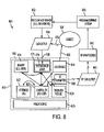
- FIG. 8 shows another exemplary system incorporating at least one imaging device constructed in accordance with another embodiment of the invention.
- FIG. 2 shows a portion of an exemplary imager 110 containing a light control function constructed in accordance with an embodiment of the invention.
- the imager 110 includes a pixel array 120 containing a plurality of pixels 122 organized in rows ROW 1 , . . . , ROW N and columns COLUMN 1 , . . . , COLUMN 256 .
- a plurality of row lines RL and column lines CL are provided for the entire array 20 .
- Pixels 122 in a same row e.g., ROW 1 are connected to row selection circuitry 132 by respective row lines RL.
- COLUMN 256 are connected by a respective column line CL to a dedicated sampling capacitors and switches 140 1 , . . . , 140 256 (collectively “sampling capacitors and switches 140 ”) for that column COLUMN 1 , . . . , COLUMN 256 .
- the imager 110 also includes a plurality of comparators 160 1 , . . . , 160 64 (collectively “comparators 160 ”).
- comparators 160 there are sixty-four comparators 160 , one for every four columns of the pixel array 120 .
- the invention is not limited to a specific number of comparators 160 .
- the inventors have determined that sixty-four comparators 160 , connected to sixty-four different columns is desirable.
- the first comparator 160 1 is connected to the column line CL of the first column COLUMN 1
- the second comparator 160 2 is connected to the column line CL of the fifth column, etc.
- the last comparator 160 64 is connected to the column line CL of the 253rd column COLUMN 253 .
- a “scan” as used herein is a sequence of consecutive row selections.
- the comparators 160 are connected to the set of pixels 122 in the dedicated columns e.g., COLUMN 1 , COLUMN 5 , . . . , COLUMN 253 .
- the comparators 160 receive pixel signals from their respective column lines CL.
- the pixel signals are used to determine the present illumination of the pixels 122 of the respective columns.
- the comparators 160 are also connected to a voltage reference generator 170 that outputs a reference voltage V ref to be compared against the pixels signals. As is discussed below, the voltage reference generator 170 is controllable to output different reference voltages V ref when desired. Each comparator 160 outputs one logic value (e.g., logical “1”) when its respective pixel signal exceeds the reference voltage V ref and a second different logical value (e.g., logical “0”) when its respective pixel signal has not exceeded the reference voltages V ref .
- a logic value e.g., logical “1”
- a second different logical value e.g., logical “0”
- a bit collection circuit 162 is used to collect the results of the comparators 160 and to output the results to a counter 164 .
- the counter 164 counts the number of pixels that have exceeded the reference voltage V ref in a single scan (e.g., the predetermined number of consecutively selected rows).
- the output of the counter 164 is used by a digital logic block 166 and compared to a predetermined number of pixels in the block 166 .
- the digital block 166 may output an analog gain value ANALOG GAIN and/or an illumination stop signal ILLUMINATION STOP.
- the analog gain value ANALOG GAIN is used during pixel readout to ensure that the appropriate signal strength is used during the readout process.
- the illumination stop signal ILLUMINATION STOP is used to end the exposure period for all of the pixels 122 in the array 120 (i.e., stop the exposure of light onto the pixels 122 ).
- the imager 110 also includes a differential amplifier (e.g., amplifier 40 of FIG. 1 ), an analog-to-digital converter (e.g., ADC 45 of FIG. 1 ) and an image processor (e.g., processor 50 of FIG. 1 ).
- the sample and hold circuit samples and holds pixel reset V rst and a pixel image signals V sig for selected pixels.
- the differential amplifier produces a differential signal (V rst ⁇ V sig ) for each pixel, which is digitized by the analog-to-digital converter
- the digitized pixel signals are input by the image processor and output as a digital image.
- FIG. 3 illustrates an exemplary method 200 of performing automatic light control in accordance with an embodiment of the invention.
- the method 200 has some desirable requirements that enable it to achieve automatic light control in a quick, efficient, real-time and non-destructive manner.
- method 200 uses a measurement time that is part of and no greater than the total exposure time. Keeping the measurement time within the boundaries of the total exposure helps conserve power. Another desirable requirement is that the measurements taken during execution of method 200 are performed on a subset of pixels, rather than the entire array. The measurements are non-destructive, which means that the pixels are not reset during the exposure.
- the method 200 seeks to obtain a predefined number of pixels having a predefined signal level (discussed in more detail below). To ensure a fast light control process, method 200 uses analog pixel signals rather than using analog-to-digital converted pixel signals. The method 200 will not include pixels having “white spots” (i.e., pixels with defects or extremely high dark current) in its final light control determination.
- the method 200 uses programmable (i.e., adjustable parameters) such as e.g., the analog gain required during pixel readout, required number of pixels at the predefined signal level (“P r ”), preferred exposure time (“t 1 ”) and maximum exposure time (“t m ”). “Exposure time” is the time the light source is illuminated.
- method 200 continuously scans the predefined pixels during the exposure period. Decisions on the readout gain and exposure time settings are made based on the time intervals when the required number of pixels P r reach the reference level V ref (if they reach the level at all). Adjustments to certain parameters, including the reference level V ref , maximum exposure time t m and gain, may be made during the exposure period.
- the required number of pixels at the predefined signal level P r must be set.
- the preferred exposure time t 1 and maximum exposure time t m must also be set.
- the values for the required number of pixels P r , preferred exposure time t 1 and maximum exposure time t m are application specific and the invention is not to be limited to any specific values for these parameters.
- the maximum exposure time t m limits the exposure duration to prevent blurring of the images.
- the timing values used to determine changes in the reference level (V ref ) and gain are determined based on the preferred exposure time t 1 .
- Execution of method 200 begins by setting the reference level V ref (step 202 ).
- V ref is set to V fs /G max , where V fs is the full scale signal and G max is the maximum gain that can be used.
- An exemplary value for V fs is 1V and an exemplary value for G max is 4.
- the exposure is started and the current exposure time t is set to 0 (step 204 ).
- the exposure period is the integration period.
- the start of the exposure period is the start of the integration period (which could be activated by a shutter or some other method known in the art).
- All of the predefined pixels are scanned (step 206 ) during an exposure (or integration period).
- the pixel signals V sig from all the predefined scanned pixels are sent via a respective column line to a respective comparator.
- the present time t is compared to the maximum exposure time t m (step 208 ). If the present time t is greater than the maximum exposure time t m , the method continues at step 218 where the gain is set to maximum gain G max .
- the exposure is stopped (i.e., the digital block 166 of FIG. 2 outputs the illumination stop signal ILLUMINATION STOP to turn off the illumination devices or to end the integration period, depending upon the application)(step 220 ) and the method 200 ends.
- the new gain setting is reflected as line ‘a’ in FIG. 4 , which is a graph of gain settings and pixel output level versus time.
- solid lines 402 , 404 and 406 reflect respective gain limits for the various pixel output versus time combinations. Specifically, line 402 reflects the gain limit set to the minimum gain G min , line 404 represents the gain limit G 2 (a gain halfway between the maximum and minimum) and line 406 reflects the gain limit set to the minimum gain G max .
- step 208 if at step 208 the present time t is not greater than the maximum exposure time t m , the method continues at step 210 where, for each predefined pixel, each comparator determines if the pixel signal V sig is greater than the reference level V ref . If a required number of pixels P r of the predefined number of pixels do not have a pixel signal V sig that is greater than the reference level V ref (step 210 ), the method 200 continues at step 206 where all of the predefined pixels are scanned once again.
- step 210 If the required number of pixels P r of the predefined number of pixels have a pixel signal V sig that is greater than the reference level V ref (step 210 ) the method 200 continues at step 212 to determine the appropriate light control action.
- the readout gain is set to the minimum gain G min and the reference level V ref is set to V fs (step 214 ).
- the new gain setting is reflected as line ‘b’ in FIG. 4 .
- the exposure is allowed to continue. As such, the method 200 continues at step 222 where all of the predefined pixels are scanned again.
- step 224 If a required number of pixels P r of the predefined number of pixels do not have a pixel signal V sig that is greater than the reference level V ref (step 224 ), the method 200 continues at step 226 to determine if the present time t is greater than the maximum exposure time t m .
- the method 200 continues at step 222 . If it is determined that the present time t is greater than the maximum exposure time t m (step 226 ) or that required number of pixels P r have a pixel signal V sig that is greater than the reference level V ref (step 224 ), the exposure is stopped (step 220 ) and the method 200 terminates.
- the readout gain is set to G 2 (i.e., the gain halfway between the maximum and minimum gains)
- the reference level V ref is set to V fs /G 2 (step 216 )
- the exposure is allowed to continue.
- the method 200 continues at step 222 where all of the predefined pixels are scanned again (as discussed above).
- the new gain setting is reflected as line ‘c’ in FIG. 4 .
- the readout gain is set to the maximum gain G max (step 218 ) and the exposure is stopped (step 220 ).
- the new gain setting is reflected as line ‘d’ in FIG. 4 .
- the illumination on the pixels is monitored in real-time, with adjustments to exposure time duration and readout gain (if necessary).
- Present illumination on the pixels is determined in a non-destructive manner. That is, the signal level of the pixels is not altered or effected in any manner so that the eventual digital image reflects the image captured by the pixels.
- the method 200 conserves power by only utilizing the light source during the exposure period (as opposed to illuminating the light source prior to and longer than the exposure period).
- the rows are scanned sequentially, but the invention is not so limited.
- the columns are checked in parallel by comparing the pixel signals to the reference level in the comparators 160 ( FIG. 2 ).
- the pixel is typically reset before the exposure.
- the pixel signal output level V out begins at the reset voltage V rst .
- the pixel output signal level in absolute voltage
- the pixel signal V sig V rst ⁇ V out .
- the reference voltage presented to the comparators is the voltage (referred to ground) that represents the pixel output voltage V pix-th (referred to ground) at the desired signal level V th (referred to reset level).
- the reference level V ref is V fs /gain, ideally referenced against V rst .
- V rst is not available during the exposure.
- an average reset level V rst,mean is used during the exposure period.
- V rst,mean is the average reset level from a set of dark (i.e., light shielded) pixels outside or at the border of the image area.
- the pixel signal level is given as the difference between the pixel reset level and the instantaneous pixel output voltage, and will this be a positive voltage increasing from 0 during exposure.
- the results of the first scan of the predetermined pixels (which in the illustrated embodiment is 640 pixels) is used as a check for “white spots.” These pixels are not allowed to contribute to the light control determinations effecting gain and exposure time settings.
- the method 200 may be modified to scan additional pixels to compensate for the “white spot” pixels.
- method 200 may include the option to check for a predetermined number of saturated pixels after each scanned line, or at other intervals based on selected rows, to terminate the scan before it completes. This option increases the exposure time resolution.
- the supply voltage in the exposure period may be different from the supply voltage during pixel readout. This means that the pixel reset level may not be correct during exposure.
- the voltage reference generator 170 according to the invention ( FIG. 5 ) compensates for this.
- the generator 170 includes several sample and hold switches 502 , 504 , 506 , 512 , 514 , 516 , capacitors 508 , 518 , 524 , 528 , 534 , 544 , three amplifiers 510 , 520 , 526 and additional switches S 1 , S 2 .
- a mean reset value V rst,mean from a set of dummy pixels is sampled and stored on capacitor 508 just before the light is illuminated (or the integration period begins).
- a low droop rate is required as the reset level V rst,mean must be valid throughout the complete light control method 200 .
- the sampled value V rst,mean is buffered in amplifier 510 and feedback to the switch 506 terminal and to the first sampling capacitor 508 .
- the generation of the reference V ref is done by subtraction of the predefined fraction of the full scale signal V fs from the average reset level V rst,mean .
- V fs is divided by the readout gains 1 , 2 , or 4 according to the position of the switches S 1 , S 2 .
- FIG. 6 illustrates another exemplary imager 610 constructed in accordance with another exemplary embodiment of the invention.
- the illustrated imager 610 compensates for comparator input offsets, which may be present in the imager 110 illustrated in FIG. 2 .
- the illustrated imager 610 uses half the number of comparators 660 1 , 660 2 , . . . , 660 32 that are used in the FIG. 2 imager 110 .
- the illustrated imager 610 compares columns in two consecutive phases. In phase one, the outputs from the first half of the columns (e.g., column 1 , column 9 , . . . , column 249 ) are input into the comparators 660 1 , 660 2 , . . .
- 660 32 via input switches 661 1b , 661 2b , . . . , 661 32b and tested against the reference level V ref via input switches 661 1a , 661 2a , . . . , 661 32a .
- the results are output from an inverted output of the comparators 660 1 , 660 2 , . . . , 660 32 to the bit collection unit 662 via switches 663 1 , 663 2 , . . . , 663 32 .
- FIG. 7 shows system 700 , a typical processor system modified to include an imaging device 708 constructed in accordance with an embodiment of the invention (i.e., imager 110 of FIG. 2 , imager 610 of FIG. 6 ).
- the processor-based system 700 is exemplary of a system having digital circuits that could include image sensor devices. Without being limiting, such a system could include a computer system, camera system, scanner, machine vision, vehicle navigation, video phone, surveillance system, auto focus system, star tracker system, motion detection system, image stabilization system, and data compression system.
- System 700 for example a camera system, generally comprises a central processing unit (CPU) 702 , such as a microprocessor, that communicates with an input/output (I/O) device 706 over a bus 704 .
- Imaging device 708 also communicates with the CPU 702 over the bus 704 .
- the processor-based system 700 also includes random access memory (RAM) 710 , and can include removable memory 715 , such as flash memory, which also communicate with the CPU 702 over the bus 704 .
- the imaging device 708 may be combined with a processor, such as a CPU, digital signal processor, or microprocessor, with or without memory storage on a single integrated circuit or on a different chip than the processor.
- FIG. 8 shows another exemplary system 800 having a device 810 incorporating an imager chip 812 constructed in accordance with an embodiment of the invention (i.e., imager 110 of FIG. 2 , imager 610 of FIG. 6 ).
- the imager chip 812 can include a photosensor array 814 , photosensor interface 815 , memory circuit 816 , and a controller 820 integrated on the same silicon chip.
- the photosensor interface 815 can be controlled by the controller 820 for addressing the array 814 .
- the system 800 is constructed and operated as described in copending U.S. application Ser. No. 10/143,578.
- the memory circuit 816 can communicate with the other operational circuits of the device 810 , including, but not limited to, the controller 820 (e.g., an 8051 controller), a serializer module 824 , extended shift registers SFRs 822 , and an RF (radio frequency) transmitter 828 .
- the memory circuit 816 is capable of storing operational information for the photosensor array 814 and all other circuitry incorporated into the device 810 . Further, the memory circuit 816 is be capable of storing images received by the photosensor array 814 .
- the controller 820 operates as the “brain” of the device 810 using programming and/or data stored in the memory circuit 816 , and/or in an internal ROM.
- the controller 820 can utilize the stored programs and/or data in controlling the acquiring of images, the storing of images, and the communication of images to an external system for viewing.
- the CMOS photosensor array 814 can download captured images, like a camera. However, the CMOS photosensor array 814 of the invention can also download programming and/or operational information as data-input 834 , such as software, programming, or other useful data.
- a user can select the data desired to be downloaded by utilizing a program command system 830 , which can contain a collection of programs, instructions, software, or other data that can be utilized by the device 810 .
- the program command system 830 which can be a standard computer, communicates to a photo-data generator 832 , which can be any device capable of outputting light signals, for instance, a computer monitor (CRT) connected to a computer, or an LED unit.
- the photo-data generator 832 can output light at various wavelengths (colors) and intensities, and in various patterns.
- the photo-data generator 832 generates light 836 , which is input to photosensor array 814 during a period when it is not acquiring images. This period can be controlled and designated by the controller 820 .
- the light 836 can be varied in any means known in the art so that it corresponds to the data desired to be downloaded into the device 810 .
- the light can be varied in color, where different colors or color patterns can be read by the photosensor array 814 , stored in the memory circuit 16 , and interpreted by the controller 820 of the device 810 , via communication with the photosensor array 814 , as different digital information (i.e., “1s” and “0s”).
- the memory circuit 814 , and device 810 in general, can be programmed by a user with the input of light 836 to the photosensor array 814 .
- the device 810 functions as an imager camera.
- the camera function of the device 810 is like that of any other CMOS imager camera to acquire still frames or constant motion video.
- the LED(s) 818 can function as light strobes during camera use, and be synchronized with the image acquisition by the photosensor array 814 .
- Light 836 from the LED 818 can illuminate a subject 838 within an image area to be captured.
- the reflected light 836 from the illuminated subject 838 can be acquired by the photosensor array 814 .
- the images acquired by the photosensor array 814 are communicated to and translated by the serializer module 824 into a format for image output.
- the memory circuit 816 can store programming and/or data so that the controller 820 can use the input programs and/or data acquired during the data input operation to direct the operation of the photosensor array 814 , the serializer module 824 , and the extended SFRs 822 (all of which can be in communication with the memory circuit 816 and controller 820 ) for image capture, storage, processing, and output.
- the stored images can be translated into an RF data output 840 generated by an RF transmitter 828 in communication with the serializer module 824 under control of the controller 820 .
- the images, as RF data output 840 are transmitted to an RF data receiver 842 .
- the RF data receiver 842 is in communication with the program command system 830 so that a user can receive the images acquired by the photosensor array 814 for viewing, for example on the same computer monitor (i.e., photo-data generator 832 ) that could be used to initially program the device 810 .
- the device 810 is incorporated into a swallowable pill as described in copending U.S. application Ser. No. 10/143,578.
Abstract
Description
Claims (20)
Priority Applications (5)
| Application Number | Priority Date | Filing Date | Title |
|---|---|---|---|
| US10/846,513 US7605852B2 (en) | 2004-05-17 | 2004-05-17 | Real-time exposure control for automatic light control |
| US11/052,217 US20050253937A1 (en) | 2004-05-17 | 2005-02-08 | Real-time exposure control for automatic light control |
| US12/560,135 US8149326B2 (en) | 2004-05-17 | 2009-09-15 | Real-time exposure control for automatic light control |
| US13/403,599 US8547476B2 (en) | 2004-05-17 | 2012-02-23 | Image sensor including real-time automatic exposure control and swallowable pill including the same |
| US14/036,437 US9071762B2 (en) | 2004-05-17 | 2013-09-25 | Image sensor including real-time automatic exposure control and swallowable pill including the same |
Applications Claiming Priority (1)
| Application Number | Priority Date | Filing Date | Title |
|---|---|---|---|
| US10/846,513 US7605852B2 (en) | 2004-05-17 | 2004-05-17 | Real-time exposure control for automatic light control |
Related Child Applications (3)
| Application Number | Title | Priority Date | Filing Date |
|---|---|---|---|
| US11/052,217 Continuation-In-Part US20050253937A1 (en) | 2004-05-17 | 2005-02-08 | Real-time exposure control for automatic light control |
| US12/560,135 Continuation US8149326B2 (en) | 2004-05-17 | 2009-09-15 | Real-time exposure control for automatic light control |
| US12/560,135 Division US8149326B2 (en) | 2004-05-17 | 2009-09-15 | Real-time exposure control for automatic light control |
Publications (2)
| Publication Number | Publication Date |
|---|---|
| US20050253944A1 US20050253944A1 (en) | 2005-11-17 |
| US7605852B2 true US7605852B2 (en) | 2009-10-20 |
Family
ID=35309029
Family Applications (4)
| Application Number | Title | Priority Date | Filing Date |
|---|---|---|---|
| US10/846,513 Active 2028-08-20 US7605852B2 (en) | 2004-05-17 | 2004-05-17 | Real-time exposure control for automatic light control |
| US12/560,135 Active US8149326B2 (en) | 2004-05-17 | 2009-09-15 | Real-time exposure control for automatic light control |
| US13/403,599 Active US8547476B2 (en) | 2004-05-17 | 2012-02-23 | Image sensor including real-time automatic exposure control and swallowable pill including the same |
| US14/036,437 Active US9071762B2 (en) | 2004-05-17 | 2013-09-25 | Image sensor including real-time automatic exposure control and swallowable pill including the same |
Family Applications After (3)
| Application Number | Title | Priority Date | Filing Date |
|---|---|---|---|
| US12/560,135 Active US8149326B2 (en) | 2004-05-17 | 2009-09-15 | Real-time exposure control for automatic light control |
| US13/403,599 Active US8547476B2 (en) | 2004-05-17 | 2012-02-23 | Image sensor including real-time automatic exposure control and swallowable pill including the same |
| US14/036,437 Active US9071762B2 (en) | 2004-05-17 | 2013-09-25 | Image sensor including real-time automatic exposure control and swallowable pill including the same |
Country Status (1)
| Country | Link |
|---|---|
| US (4) | US7605852B2 (en) |
Cited By (5)
| Publication number | Priority date | Publication date | Assignee | Title |
|---|---|---|---|---|
| US20080055426A1 (en) * | 2006-08-29 | 2008-03-06 | Shimon Pertsel | Digital Camera with Selectively Increased Dynamic Range By Control of Parameters During Image Acquisition |
| US20080055440A1 (en) * | 2006-08-29 | 2008-03-06 | Shimon Pertsel | Wide Dynamic Range Image Capturing System Method and Apparatus |
| US8150255B2 (en) * | 2010-06-25 | 2012-04-03 | Apple Inc. | Flash control for electronic rolling shutter |
| US9762809B2 (en) * | 2015-08-28 | 2017-09-12 | Renesas Electronics Corporation | Semiconductor device |
| US11730352B2 (en) | 2021-01-13 | 2023-08-22 | Hong Kong Applied Science and Technology Research Institute Company Limited | Auto-exposure method for wireless capsule endoscope |
Families Citing this family (22)
| Publication number | Priority date | Publication date | Assignee | Title |
|---|---|---|---|---|
| JP4311181B2 (en) * | 2003-12-05 | 2009-08-12 | ソニー株式会社 | Semiconductor device control method, signal processing method, semiconductor device, and electronic apparatus |
| US7227117B1 (en) * | 2006-05-30 | 2007-06-05 | Symbol Technologies, Inc. | High speed auto-exposure control |
| US7738019B2 (en) * | 2006-10-11 | 2010-06-15 | Avago Technologies General Ip (Singapore) Pte. Ltd. | System and method for providing automatic gain control in an imaging device |
| JP2008211591A (en) * | 2007-02-27 | 2008-09-11 | Seiko Instruments Inc | Photoelectric converter |
| US10368053B2 (en) | 2012-11-14 | 2019-07-30 | Qualcomm Incorporated | Structured light active depth sensing systems combining multiple images to compensate for differences in reflectivity and/or absorption |
| US8982238B2 (en) | 2013-07-02 | 2015-03-17 | Omnivision Technologies, Inc. | Multi-target automatic exposure and gain control based on pixel intensity distribution |
| FR3025086B1 (en) | 2014-09-02 | 2016-11-11 | E2V Semiconductors | METHOD AND SYSTEM FOR TAKING MEDICAL RADIOLOGICAL IMAGES WITH STOP CONTROL OF THE X-RAY SOURCE |
| JP5927370B1 (en) * | 2014-09-05 | 2016-06-01 | オリンパス株式会社 | Imaging apparatus and processing apparatus |
| TWI514875B (en) * | 2014-10-21 | 2015-12-21 | Avision Inc | Image sensing device |
| JP6482318B2 (en) * | 2015-02-26 | 2019-03-13 | ジックオプテックス株式会社 | Optical displacement meter |
| CN104754240B (en) * | 2015-04-15 | 2017-10-27 | 中国电子科技集团公司第四十四研究所 | Cmos image sensor automatic explosion method and device |
| CN108024688B (en) * | 2015-07-15 | 2020-07-24 | 奥林巴斯株式会社 | Shape calculation device |
| US9936151B2 (en) * | 2015-10-16 | 2018-04-03 | Capsovision Inc | Single image sensor for capturing mixed structured-light images and regular images |
| JP2017098698A (en) * | 2015-11-20 | 2017-06-01 | セイコーエプソン株式会社 | Imaging apparatus, electronic apparatus, and imaging method |
| CN108606804A (en) * | 2016-12-13 | 2018-10-02 | 上海西门子医疗器械有限公司 | The automated calibration system and method and Medical Devices of auto-exposure control |
| JP6872028B2 (en) * | 2017-09-08 | 2021-05-19 | 富士フイルム株式会社 | Imaging control device, imaging device, imaging control method, and imaging control program |
| US10965894B2 (en) * | 2017-11-20 | 2021-03-30 | Flir Commercial Systems, Inc. | Short wave infrared image sensor with automatic exposure and dynamic range control |
| CN107819991A (en) * | 2017-11-27 | 2018-03-20 | 成都力鑫科技有限公司 | Dynamic exposure is set to compensate digital camera method |
| US20220413167A1 (en) * | 2019-11-29 | 2022-12-29 | Lg Electronics Inc. | Radiation detector and radiographic method using same |
| CN111131723A (en) * | 2019-12-31 | 2020-05-08 | 佛山喀视科技有限公司 | Ceramic tile image acquisition method and system |
| CN111539321A (en) * | 2020-04-22 | 2020-08-14 | 中国飞机强度研究所 | Force sensor serial number checking system and method |
| CN113259600B (en) * | 2021-05-11 | 2022-08-05 | 北京地平线机器人技术研发有限公司 | Exposure parameter configuration method and device, electronic equipment and medium |
Citations (8)
| Publication number | Priority date | Publication date | Assignee | Title |
|---|---|---|---|---|
| US20030117491A1 (en) | 2001-07-26 | 2003-06-26 | Dov Avni | Apparatus and method for controlling illumination in an in-vivo imaging device |
| US20030210439A1 (en) | 2002-05-13 | 2003-11-13 | Atif Sarwari | Data download to imager chip using image sensor as a receptor |
| US20030210334A1 (en) | 2002-05-13 | 2003-11-13 | Atif Sarwari | Integrated CMOS imager and microcontroller |
| US20030211405A1 (en) | 2002-05-13 | 2003-11-13 | Kartik Venkataraman | Color filter imaging array and method of formation |
| WO2004082472A1 (en) | 2003-03-23 | 2004-09-30 | Given Imaging Ltd. | Apparatus and method for light control in an in-vivo imaging device |
| US6831689B2 (en) * | 1998-10-19 | 2004-12-14 | Orly Yadid-Pecht | Optical imager using a method for adaptive real-time expanding of the dynamic range |
| US7053954B1 (en) * | 1998-10-23 | 2006-05-30 | Datalogic S.P.A. | Process for regulating the exposure time of a light sensor |
| US7099056B1 (en) * | 2002-04-03 | 2006-08-29 | Eastman Kodak Company | Automatically balanced exposure time and gain in an image sensor |
Family Cites Families (167)
| Publication number | Priority date | Publication date | Assignee | Title |
|---|---|---|---|---|
| US53954A (en) * | 1866-04-17 | Stove-pipe drum | ||
| US2240312A (en) | 1940-02-24 | 1941-04-29 | Herbert A Minturn | Means for adjusting tractor wheels |
| US3683389A (en) | 1971-01-20 | 1972-08-08 | Corning Glass Works | Omnidirectional loop antenna array |
| JPS5028002Y2 (en) | 1971-02-05 | 1975-08-19 | ||
| US3723644A (en) | 1972-04-24 | 1973-03-27 | Bell Telephone Labor Inc | Variable frame rate recording system using speed measurement |
| US3971362A (en) | 1972-10-27 | 1976-07-27 | The United States Of America As Represented By The Administrator Of The National Aeronautics And Space Administration | Miniature ingestible telemeter devices to measure deep-body temperature |
| JPS5015515A (en) | 1973-06-07 | 1975-02-19 | ||
| US3984628A (en) | 1975-01-13 | 1976-10-05 | Paul Grayson Sharp | Remote camera-position control |
| JPS51135840A (en) | 1975-05-21 | 1976-11-25 | Nippon Packaging Kk | Surface treatment process for zinc or zinc alloy |
| JPS5519124A (en) | 1978-07-27 | 1980-02-09 | Olympus Optical Co | Camera system for medical treatment |
| JPS5594235A (en) | 1979-01-11 | 1980-07-17 | Olympus Optical Co | Endoscope photographing device |
| JPS6043711B2 (en) | 1979-03-14 | 1985-09-30 | オリンパス光学工業株式会社 | Imaging device |
| US4273431A (en) | 1979-08-02 | 1981-06-16 | Polaroid Corporation | Adapter for coupling a photographic camera with a viewing device |
| JPS5764348A (en) | 1980-10-06 | 1982-04-19 | Sony Corp | Mode switching device of recorder and reproducer |
| JPS5795771A (en) | 1980-12-05 | 1982-06-14 | Fuji Photo Film Co Ltd | Solid-state image pickup device |
| JPS58172078A (en) | 1982-04-02 | 1983-10-08 | Sony Corp | Reproducing device |
| DE3337455A1 (en) | 1982-10-15 | 1984-04-19 | Olympus Optical Co., Ltd., Tokio/Tokyo | ENDOSCOPIC PHOTOGRAPHER |
| US4532918A (en) | 1983-10-07 | 1985-08-06 | Welch Allyn Inc. | Endoscope signal level control |
| JP2655568B2 (en) | 1984-08-31 | 1997-09-24 | オリンパス光学工業株式会社 | Endoscope using solid-state imaging device |
| DE3440177A1 (en) | 1984-11-02 | 1986-05-15 | Friedrich Dipl.-Ing. 8031 Eichenau Hilliges | Television recording and replay device for endoscopy on human and animal bodies |
| US4786982A (en) | 1984-12-28 | 1988-11-22 | Sony Corporation | Multi-function rotary dial system including timer setting feature |
| US4689621A (en) | 1986-03-31 | 1987-08-25 | The United States Of America As Represented By The Administrator Of The National Aeronautics And Space Administration | Temperature responsive transmitter |
| JPH0664243B2 (en) | 1986-04-30 | 1994-08-22 | オリンパス光学工業株式会社 | Endoscope |
| US4854328A (en) | 1987-03-23 | 1989-08-08 | Philip Pollack | Animal monitoring telltale and information system |
| JPS63294826A (en) | 1987-05-27 | 1988-12-01 | Olympus Optical Co Ltd | Endoscopic apparatus |
| US4841291A (en) | 1987-09-21 | 1989-06-20 | International Business Machines Corp. | Interactive animation of graphics objects |
| JP2598422B2 (en) | 1987-09-30 | 1997-04-09 | オリンパス光学工業株式会社 | Endoscope device |
| US5189519A (en) | 1988-03-22 | 1993-02-23 | Canon Kabushiki Kaisha | Electronic camera with exposure control |
| US4844076A (en) | 1988-08-26 | 1989-07-04 | The Johns Hopkins University | Ingestible size continuously transmitting temperature monitoring pill |
| JP2579372B2 (en) | 1989-12-04 | 1997-02-05 | 日本テキサス・インスツルメンツ株式会社 | Low power imaging device |
| US5875280A (en) | 1990-03-29 | 1999-02-23 | Canon Kabushiki Kaisha | Recording apparatus having variably settable compression ratio |
| US5596366A (en) | 1990-05-14 | 1997-01-21 | Canon Kabushiki Kaisha | Camera apparatus having camera movement detection |
| US5202961A (en) | 1990-06-08 | 1993-04-13 | Apple Computer, Inc. | Sequential information controller |
| US5268564A (en) | 1990-08-03 | 1993-12-07 | Symbol Technologies, Inc. | Bar code scanner actuated by detection of scanner motion |
| JPH04109927A (en) | 1990-08-31 | 1992-04-10 | Toshiba Corp | Electronic endoscope apparatus |
| JP3164609B2 (en) | 1990-10-31 | 2001-05-08 | オリンパス光学工業株式会社 | Endoscope device |
| JP2948900B2 (en) | 1990-11-16 | 1999-09-13 | オリンパス光学工業株式会社 | Medical capsule |
| JP3041099B2 (en) | 1991-02-01 | 2000-05-15 | オリンパス光学工業株式会社 | Electronic endoscope device |
| US5351161A (en) | 1991-04-03 | 1994-09-27 | Sony Electronics, Inc. | Variable scale rotary switch |
| US5279607A (en) | 1991-05-30 | 1994-01-18 | The State University Of New York | Telemetry capsule and process |
| EP0526064B1 (en) | 1991-08-02 | 1997-09-10 | The Grass Valley Group, Inc. | Video editing system operator interface for visualization and interactive control of video material |
| US5355450A (en) | 1992-04-10 | 1994-10-11 | Avid Technology, Inc. | Media composer with adjustable source material compression |
| DE69330513D1 (en) | 1992-03-20 | 2001-09-06 | Commw Scient Ind Res Org | OBJECT MONITORING SYSTEM |
| US5585840A (en) | 1992-06-11 | 1996-12-17 | Olympus Optical Co., Ltd. | Endoscope apparatus in which image pickup means and signal control means are connected to each other by signal transmitting means |
| US5408263A (en) | 1992-06-16 | 1995-04-18 | Olympus Optical Co., Ltd. | Electronic endoscope apparatus |
| JP3275058B2 (en) | 1992-07-10 | 2002-04-15 | 三菱電機株式会社 | Video camera |
| US5643175A (en) | 1992-09-01 | 1997-07-01 | Adair; Edwin L. | Sterilizable endoscope with separable disposable tube assembly |
| US5423312A (en) | 1992-12-18 | 1995-06-13 | Schott Fiber Optics, Inc. | Rigid endoscope having modified high refractive index tunnel rod for image transmission and method of manufacture thereof |
| US5678568A (en) | 1993-07-27 | 1997-10-21 | Olympus Optical Co., Ltd. | System control apparatus, medical system control apparatus and image-plane display method of medical system control apparatus |
| US5749830A (en) | 1993-12-03 | 1998-05-12 | Olympus Optical Co., Ltd. | Fluorescent endoscope apparatus |
| IL108352A (en) | 1994-01-17 | 2000-02-29 | Given Imaging Ltd | In vivo video camera system |
| US5819736A (en) | 1994-03-24 | 1998-10-13 | Sightline Technologies Ltd. | Viewing method and apparatus particularly useful for viewing the interior of the large intestine |
| JPH07275200A (en) | 1994-04-15 | 1995-10-24 | Asahi Optical Co Ltd | Illuminator for endoscope |
| JPH08555A (en) | 1994-06-16 | 1996-01-09 | Fuji Photo Optical Co Ltd | Illumination device of endoscope |
| JP3782107B2 (en) | 1994-11-30 | 2006-06-07 | ボストン サイエンティフィック リミテッド | Acoustic imaging, Doppler catheters and guidewires |
| JPH08313823A (en) | 1995-05-15 | 1996-11-29 | Olympus Optical Co Ltd | Endoscopic image processing device |
| US5833603A (en) | 1996-03-13 | 1998-11-10 | Lipomatrix, Inc. | Implantable biosensing transponder |
| US5853005A (en) | 1996-05-02 | 1998-12-29 | The United States Of America As Represented By The Secretary Of The Army | Acoustic monitoring system |
| US5738110A (en) | 1996-05-29 | 1998-04-14 | Beal; Charles B. | Device for the diagnosis of certain gastrointestinal pathogens |
| US6078353A (en) | 1996-09-12 | 2000-06-20 | Fuji Photo Optical Co., Ltd. | All-pixels reading type electronic endoscope apparatus |
| GB9619470D0 (en) | 1996-09-18 | 1996-10-30 | Univ London | Imaging apparatus |
| JP3428315B2 (en) | 1996-10-08 | 2003-07-22 | 株式会社東芝 | Disc playback device |
| ES2208963T3 (en) | 1997-01-03 | 2004-06-16 | Biosense, Inc. | PRESSURE SENSITIVE VASCULAR ENDOPROTESIS. |
| JP3351704B2 (en) | 1997-04-09 | 2002-12-03 | ペンタックス株式会社 | Image signal correction device |
| US5873830A (en) | 1997-08-22 | 1999-02-23 | Acuson Corporation | Ultrasound imaging system and method for improving resolution and operation |
| EP0908137A1 (en) | 1997-10-06 | 1999-04-14 | Technologiestichting STW | A method and apparatus for making an image of a lumen or other body cavity and its surrounding tissue |
| US6310642B1 (en) | 1997-11-24 | 2001-10-30 | Micro-Medical Devices, Inc. | Reduced area imaging devices incorporated within surgical instruments |
| JPH11111795A (en) | 1997-10-07 | 1999-04-23 | Ricoh Co Ltd | Inspecting device for image-pickup element |
| US6240312B1 (en) | 1997-10-23 | 2001-05-29 | Robert R. Alfano | Remote-controllable, micro-scale device for use in in vivo medical diagnosis and/or treatment |
| IL122602A0 (en) | 1997-12-15 | 1998-08-16 | Tally Eitan Zeev Pearl And Co | Energy management of a video capsule |
| US6364829B1 (en) | 1999-01-26 | 2002-04-02 | Newton Laboratories, Inc. | Autofluorescence imaging system for endoscopy |
| US6254531B1 (en) | 1998-03-10 | 2001-07-03 | Fuji Photo Optical Co., Ltd. | Electronic-endoscope light quantity controlling apparatus |
| JPH11265249A (en) | 1998-03-17 | 1999-09-28 | Toshiba Corp | Information input device, information input method and storage medium |
| JPH11290269A (en) | 1998-04-09 | 1999-10-26 | Olympus Optical Co Ltd | Solid photographing apparatus |
| US6462770B1 (en) | 1998-04-20 | 2002-10-08 | Xillix Technologies Corp. | Imaging system with automatic gain control for reflectance and fluorescence endoscopy |
| JPH11305144A (en) | 1998-04-27 | 1999-11-05 | Olympus Optical Co Ltd | Endoscope device |
| WO2000010456A1 (en) | 1998-08-02 | 2000-03-02 | Super Dimension Ltd. | Intrabody navigation system for medical applications |
| JP2000059677A (en) | 1998-08-06 | 2000-02-25 | Minolta Co Ltd | Digital camera |
| US6402689B1 (en) | 1998-09-30 | 2002-06-11 | Sicel Technologies, Inc. | Methods, systems, and associated implantable devices for dynamic monitoring of physiological and biological properties of tumors |
| US6140630A (en) * | 1998-10-14 | 2000-10-31 | Micron Technology, Inc. | Vcc pump for CMOS imagers |
| US7116352B2 (en) | 1999-02-25 | 2006-10-03 | Visionsense Ltd. | Capsule |
| US8636648B2 (en) | 1999-03-01 | 2014-01-28 | West View Research, Llc | Endoscopic smart probe |
| JP4243883B2 (en) | 1999-03-15 | 2009-03-25 | フジノン株式会社 | Remote head system |
| US7355625B1 (en) | 1999-03-17 | 2008-04-08 | Olympus Corporation | Endoscopic imaging system and endoscope system |
| JP3793982B2 (en) | 1999-04-07 | 2006-07-05 | 富士写真フイルム株式会社 | Electronic camera, electronic camera finger detection method, and electronic camera level conversion method |
| WO2000074391A1 (en) | 1999-06-02 | 2000-12-07 | Vista Medical Technologies, Inc. | Interchangeable ccd camera with integral blemish compensation |
| US6376868B1 (en) * | 1999-06-15 | 2002-04-23 | Micron Technology, Inc. | Multi-layered gate for a CMOS imager |
| IL130486A (en) | 1999-06-15 | 2005-08-31 | Given Imaging Ltd | Optical system |
| US6310366B1 (en) * | 1999-06-16 | 2001-10-30 | Micron Technology, Inc. | Retrograde well structure for a CMOS imager |
| US6326652B1 (en) * | 1999-06-18 | 2001-12-04 | Micron Technology, Inc., | CMOS imager with a self-aligned buried contact |
| JP2001025004A (en) | 1999-07-09 | 2001-01-26 | Mitsuru Takashima | Electronic mirror system |
| US6204524B1 (en) * | 1999-07-14 | 2001-03-20 | Micron Technology, Inc. | CMOS imager with storage capacitor |
| GB2352636B (en) | 1999-08-03 | 2003-05-14 | Univ College London Hospitals | Improved passage-travelling device |
| IL131242A0 (en) | 1999-08-04 | 2001-01-28 | Given Imaging Ltd | A method for temperature sensing |
| US6333205B1 (en) * | 1999-08-16 | 2001-12-25 | Micron Technology, Inc. | CMOS imager with selectively silicided gates |
| WO2001019252A1 (en) | 1999-09-14 | 2001-03-22 | Hitachi Medical Corporation | Biological light measuring instrument |
| US6865718B2 (en) | 1999-09-29 | 2005-03-08 | Microsoft Corp. | Accelerated scrolling |
| JP2001112740A (en) | 1999-10-20 | 2001-04-24 | Asahi Optical Co Ltd | Capsulated endoscope |
| IL132944A (en) | 1999-11-15 | 2009-05-04 | Arkady Glukhovsky | Method for activating an image collecting process |
| IL134017A (en) | 2000-01-13 | 2008-04-13 | Capsule View Inc | Camera for viewing inside intestines |
| JP2001203910A (en) | 2000-01-20 | 2001-07-27 | Olympus Optical Co Ltd | Video signal processor |
| US7345702B2 (en) * | 2000-02-07 | 2008-03-18 | Canon Kabushiki Kaisha | Image sensing apparatus, control method for illumination device, flash photographing method, and computer program product |
| JP2001224553A (en) | 2000-02-17 | 2001-08-21 | Asahi Optical Co Ltd | Imaging instrument for capusle endoscope |
| KR100798048B1 (en) | 2000-03-08 | 2008-01-24 | 기븐 이미징 리미티드 | A capsule for in vivo imaging |
| US6709387B1 (en) | 2000-05-15 | 2004-03-23 | Given Imaging Ltd. | System and method for controlling in vivo camera capture and display rate |
| IL163684A0 (en) | 2000-05-31 | 2005-12-18 | Given Imaging Ltd | Measurement of electrical characteristics of tissue |
| JP3473552B2 (en) | 2000-06-15 | 2003-12-08 | ミノルタ株式会社 | Digital still camera |
| EP1304959A1 (en) | 2000-07-24 | 2003-05-02 | Motorola, Inc. | Ingestible electronic capsule |
| KR20030029124A (en) * | 2000-08-04 | 2003-04-11 | 포베온, 인크. | All-eletronic high-resolution digital still camera |
| JP4249479B2 (en) | 2000-09-27 | 2009-04-02 | ギブン イメージング リミテッド | Immobilizable in vivo detection device |
| US20020103425A1 (en) | 2000-09-27 | 2002-08-01 | Mault James R. | self-contained monitoring device particularly useful for monitoring physiological conditions |
| US6929636B1 (en) | 2000-11-08 | 2005-08-16 | Hewlett-Packard Development Company, L.P. | Internal drug dispenser capsule medical device |
| WO2002045567A2 (en) | 2000-12-07 | 2002-06-13 | Given Imaging Ltd. | Method and system for use of a pointing device with moving images |
| TW455738B (en) * | 2001-01-18 | 2001-09-21 | Acer Comm & Amp Multimedia Inc | Lens lid sliding device having close photographing start function |
| IL157892A0 (en) | 2001-03-14 | 2004-03-28 | Given Imaging Ltd | Method and system for detecting colorimetric abnormalities |
| WO2002080376A2 (en) | 2001-03-29 | 2002-10-10 | Given Imaging Ltd. | A method for timing control |
| WO2002082979A2 (en) | 2001-04-18 | 2002-10-24 | Bbms Ltd. | Navigating and maneuvering of an in vivo vechicle by extracorporeal devices |
| US7119814B2 (en) | 2001-05-18 | 2006-10-10 | Given Imaging Ltd. | System and method for annotation on a moving image |
| IL143260A (en) | 2001-05-20 | 2006-09-05 | Given Imaging Ltd | Array system and method for locating an in vivo signal source |
| JP4674038B2 (en) | 2001-05-20 | 2011-04-20 | ギブン イメージング リミテッド | In vivo sensing device |
| WO2002102224A2 (en) | 2001-06-18 | 2002-12-27 | Given Imaging Ltd. | In vivo sensing device with a circuit board having rigid sections and flexible sections |
| US6939292B2 (en) | 2001-06-20 | 2005-09-06 | Olympus Corporation | Capsule type endoscope |
| AU2002304266A1 (en) | 2001-06-20 | 2003-01-02 | Given Imaging Ltd. | Motility analysis within a gastrointestinal tract |
| US7083578B2 (en) | 2001-07-12 | 2006-08-01 | Given Imaging Ltd. | Device and method for examining a body lumen |
| US6934573B1 (en) | 2001-07-23 | 2005-08-23 | Given Imaging Ltd. | System and method for changing transmission from an in vivo sensing device |
| US9149175B2 (en) | 2001-07-26 | 2015-10-06 | Given Imaging Ltd. | Apparatus and method for light control in an in-vivo imaging device |
| US20030043263A1 (en) | 2001-07-26 | 2003-03-06 | Arkady Glukhovsky | Diagnostic device using data compression |
| US20060184039A1 (en) | 2001-07-26 | 2006-08-17 | Dov Avni | Apparatus and method for light control in an in-vivo imaging device |
| JP4744026B2 (en) | 2001-07-30 | 2011-08-10 | オリンパス株式会社 | Capsule endoscope and capsule endoscope system |
| IL160179A0 (en) | 2001-08-02 | 2004-07-25 | Given Imaging Ltd | Apparatus and methods for in vivo imaging |
| US7176976B2 (en) * | 2001-08-30 | 2007-02-13 | Lightsurf Technologies, Inc. | Autoexposure methodology in a digital camera |
| US6635834B1 (en) | 2001-09-19 | 2003-10-21 | Justin Bernard Wenner | System and method to delay closure of a normally closed electrical circuit |
| US6846994B2 (en) | 2001-09-19 | 2005-01-25 | Justin B. Wenner | System and method to delay closure of a normally closed electrical circuit |
| ATE532453T1 (en) | 2001-09-24 | 2011-11-15 | Given Imaging Ltd | SYSTEM FOR CONTROL OF A DEVICE IN VIVO |
| JP4885388B2 (en) | 2001-09-25 | 2012-02-29 | オリンパス株式会社 | Endoscope insertion direction detection method |
| US6859230B2 (en) * | 2001-11-07 | 2005-02-22 | Omnivision Technologies, Inc. | Method of fast automatic exposure or gain control in a MOS image sensor |
| US20030174208A1 (en) | 2001-12-18 | 2003-09-18 | Arkady Glukhovsky | Device, system and method for capturing in-vivo images with three-dimensional aspects |
| US20030195415A1 (en) | 2002-02-14 | 2003-10-16 | Iddan Gavriel J. | Device, system and method for accoustic in-vivo measuring |
| US20030197795A1 (en) * | 2002-04-22 | 2003-10-23 | Schinner Charles E. | Generation and storage of amplified video |
| WO2003094723A1 (en) | 2002-05-09 | 2003-11-20 | Given Imaging Ltd. | System and method for in vivo sensing |
| US20040254455A1 (en) | 2002-05-15 | 2004-12-16 | Iddan Gavriel J. | Magneic switch for use in a system that includes an in-vivo device, and method of use thereof |
| JP2004041709A (en) | 2002-05-16 | 2004-02-12 | Olympus Corp | Capsule medical care device |
| US7245320B2 (en) * | 2002-06-04 | 2007-07-17 | Micron Technology, Inc. | Method and apparatus for automatic gain and exposure control for maintaining target image brightness in video imager systems |
| US7708705B2 (en) | 2002-07-03 | 2010-05-04 | Given Imaging Ltd. | System and method for sensing in-vivo stress and pressure |
| JP4109927B2 (en) | 2002-08-20 | 2008-07-02 | セイコークロック株式会社 | Radio correction watch and method |
| US20040180391A1 (en) | 2002-10-11 | 2004-09-16 | Miklos Gratzl | Sliver type autonomous biosensors |
| US20040087832A1 (en) | 2002-10-30 | 2004-05-06 | Arkady Glukhovsky | Device and method for blocking activation of an in-vivo sensor |
| AU2003302076A1 (en) | 2002-11-19 | 2004-06-15 | Given Imaging Ltd. | System and method for stress and pressure sensing in an in-vivo device |
| IL159113A (en) | 2002-11-27 | 2008-11-26 | Given Imaging Ltd | Method and device of imaging with an imager having a fiber plate cover |
| JP2006507885A (en) | 2002-11-29 | 2006-03-09 | ギブン イメージング リミテッド | In vivo diagnosis method, apparatus and system |
| US7118529B2 (en) | 2002-11-29 | 2006-10-10 | Given Imaging, Ltd. | Method and apparatus for transmitting non-image information via an image sensor in an in vivo imaging system |
| WO2004054430A2 (en) | 2002-12-16 | 2004-07-01 | Given Imaging Ltd. | Device, system and method for selective activation of in vivo sensors |
| US7430011B2 (en) * | 2003-01-22 | 2008-09-30 | Omnivision Technologies, Inc. | Image sensor having dual automatic exposure control |
| US7381183B2 (en) | 2003-04-21 | 2008-06-03 | Karl Storz Development Corp. | Method for capturing and displaying endoscopic maps |
| US7214182B2 (en) | 2003-04-25 | 2007-05-08 | Olympus Corporation | Wireless in-vivo information acquiring system, body-insertable device, and external device |
| JPWO2004096022A1 (en) | 2003-04-25 | 2006-07-13 | オリンパス株式会社 | Wireless intra-subject information acquisition system and intra-subject introduction device |
| WO2004096029A1 (en) | 2003-04-25 | 2004-11-11 | Olympus Corporation | Capsule endoscope and capsule endoscope system |
| NZ545979A (en) | 2003-09-18 | 2009-02-28 | King Pharmaceuticals Res & Dev | Novel adenosine A3 receptor agonists |
| EP1690490B1 (en) | 2003-11-11 | 2012-04-18 | Olympus Corporation | Capsule type medical device system |
| JP4330981B2 (en) | 2003-11-21 | 2009-09-16 | 株式会社リガク | X-ray fluorescence analyzer |
| JP2005156216A (en) | 2003-11-21 | 2005-06-16 | Yokogawa Electric Corp | Waveform measuring instrument |
| JP5248780B2 (en) | 2003-12-31 | 2013-07-31 | ギブン イメージング リミテッド | System and method for displaying an image stream |
| US20050171418A1 (en) | 2004-01-08 | 2005-08-04 | Tah-Yeong Lin | Capsule endoscopy system |
| EP1830691A2 (en) | 2004-12-30 | 2007-09-12 | Given Imaging Ltd. | Device, system, and method for programmable in vivo imaging |
| WO2006077529A2 (en) | 2005-01-18 | 2006-07-27 | Koninklijke Philips Electronics, N.V. | System for controlling traversal of an ingested capsule |
| US20060217593A1 (en) | 2005-03-24 | 2006-09-28 | Zvika Gilad | Device, system and method of panoramic multiple field of view imaging |
| US20070106111A1 (en) | 2005-11-07 | 2007-05-10 | Eli Horn | Apparatus and method for frame acquisition rate control in an in-vivo imaging device |
-
2004
- 2004-05-17 US US10/846,513 patent/US7605852B2/en active Active
-
2009
- 2009-09-15 US US12/560,135 patent/US8149326B2/en active Active
-
2012
- 2012-02-23 US US13/403,599 patent/US8547476B2/en active Active
-
2013
- 2013-09-25 US US14/036,437 patent/US9071762B2/en active Active
Patent Citations (8)
| Publication number | Priority date | Publication date | Assignee | Title |
|---|---|---|---|---|
| US6831689B2 (en) * | 1998-10-19 | 2004-12-14 | Orly Yadid-Pecht | Optical imager using a method for adaptive real-time expanding of the dynamic range |
| US7053954B1 (en) * | 1998-10-23 | 2006-05-30 | Datalogic S.P.A. | Process for regulating the exposure time of a light sensor |
| US20030117491A1 (en) | 2001-07-26 | 2003-06-26 | Dov Avni | Apparatus and method for controlling illumination in an in-vivo imaging device |
| US7099056B1 (en) * | 2002-04-03 | 2006-08-29 | Eastman Kodak Company | Automatically balanced exposure time and gain in an image sensor |
| US20030210439A1 (en) | 2002-05-13 | 2003-11-13 | Atif Sarwari | Data download to imager chip using image sensor as a receptor |
| US20030210334A1 (en) | 2002-05-13 | 2003-11-13 | Atif Sarwari | Integrated CMOS imager and microcontroller |
| US20030211405A1 (en) | 2002-05-13 | 2003-11-13 | Kartik Venkataraman | Color filter imaging array and method of formation |
| WO2004082472A1 (en) | 2003-03-23 | 2004-09-30 | Given Imaging Ltd. | Apparatus and method for light control in an in-vivo imaging device |
Non-Patent Citations (3)
| Title |
|---|
| Bo-Rong Lin et al., "A High Dynamic Range CMOS Image Sensor Design Based on Two-Frame Composition", Electrical Engineering Department, National Tsing-Hua University. |
| David Stoppa et al., "Novel CMOS Image Sensor With a 132-dB Dynamic Range", IEEE Journal of Solid-State Circuits, vol. 37, No. 12, Dec. 2002. |
| Orly Yadid-Pect, et al., "Wide Intrascene Dynamic Range CMOS APS Using Dual Sampling", IEEE Transactions on Electron Devices, vol. 33, No. 10, Oct. 1997. |
Cited By (13)
| Publication number | Priority date | Publication date | Assignee | Title |
|---|---|---|---|---|
| US8125536B2 (en) * | 2006-08-29 | 2012-02-28 | Zoran Corporation | Wide dynamic range image capturing system method and apparatus |
| US20080055440A1 (en) * | 2006-08-29 | 2008-03-06 | Shimon Pertsel | Wide Dynamic Range Image Capturing System Method and Apparatus |
| US20100026868A1 (en) * | 2006-08-29 | 2010-02-04 | Shimon Pertsel | Wide Dynamic Range Image Capturing System Method and Apparatus |
| US7714903B2 (en) * | 2006-08-29 | 2010-05-11 | Zoran Corporation | Wide dynamic range image capturing system method and apparatus |
| US20100208101A1 (en) * | 2006-08-29 | 2010-08-19 | Zoran Corporation | Wide dynamic range image capturing system method and apparatus |
| US7872673B2 (en) * | 2006-08-29 | 2011-01-18 | Zoran Corporation | Wide dynamic range image capturing system method and apparatus |
| US20080055426A1 (en) * | 2006-08-29 | 2008-03-06 | Shimon Pertsel | Digital Camera with Selectively Increased Dynamic Range By Control of Parameters During Image Acquisition |
| US8687087B2 (en) | 2006-08-29 | 2014-04-01 | Csr Technology Inc. | Digital camera with selectively increased dynamic range by control of parameters during image acquisition |
| US8150255B2 (en) * | 2010-06-25 | 2012-04-03 | Apple Inc. | Flash control for electronic rolling shutter |
| US8401378B2 (en) | 2010-06-25 | 2013-03-19 | Apple Inc. | Flash control for electronic rolling shutter |
| US9762809B2 (en) * | 2015-08-28 | 2017-09-12 | Renesas Electronics Corporation | Semiconductor device |
| US9986172B2 (en) | 2015-08-28 | 2018-05-29 | Renesas Electronics Corporation | Semiconductor device including control signal generating circuit |
| US11730352B2 (en) | 2021-01-13 | 2023-08-22 | Hong Kong Applied Science and Technology Research Institute Company Limited | Auto-exposure method for wireless capsule endoscope |
Also Published As
| Publication number | Publication date |
|---|---|
| US20050253944A1 (en) | 2005-11-17 |
| US9071762B2 (en) | 2015-06-30 |
| US8149326B2 (en) | 2012-04-03 |
| US20100073512A1 (en) | 2010-03-25 |
| US20120154563A1 (en) | 2012-06-21 |
| US20140022368A1 (en) | 2014-01-23 |
| US8547476B2 (en) | 2013-10-01 |
Similar Documents
| Publication | Publication Date | Title |
|---|---|---|
| US8149326B2 (en) | Real-time exposure control for automatic light control | |
| US20050253937A1 (en) | Real-time exposure control for automatic light control | |
| US20240064412A1 (en) | Method and apparatus providing pixel array having automatic light control pixels and image capture pixels | |
| US6788340B1 (en) | Digital imaging control with selective intensity resolution enhancement | |
| US7099056B1 (en) | Automatically balanced exposure time and gain in an image sensor | |
| US7986363B2 (en) | High dynamic range imager with a rolling shutter | |
| US7619674B2 (en) | CMOS image sensor with wide dynamic range | |
| US7119317B2 (en) | Wide dynamic range imager with selective readout | |
| US8115841B2 (en) | Method, apparatus and system providing an image sensor having pixels with multiple exposures, diodes and gain readouts | |
| US20100321532A1 (en) | Solid-state imaging device, imaging system, and method of driving solid-state imaging device | |
| EP1657911A2 (en) | Image sensor and pixel that has switchable capacitance at the floating node | |
| US20090166515A1 (en) | Multi-point correlated sampling for image sensors | |
| EP1233612B1 (en) | CMOS image sensor with extended dynamic range | |
| US6697112B2 (en) | Imaging system having multiple image capture modes | |
| US7990426B2 (en) | Phase adjusting device and digital camera | |
| EP1067775A2 (en) | Digital imaging control with selective intensity resolution enhancement | |
| JP2005039447A (en) | Imaging device | |
| JP2007013362A (en) | Image pickup device and image pickup method | |
| EP1133168A2 (en) | Smart exposure determination for imagers | |
| JP2006197229A (en) | Image pickup device and camera | |
| JP2006121358A (en) | Solid-state image pickup device | |
| CN117499802A (en) | Image sensor performing selective multisampling and method of operating the same | |
| US20170026591A1 (en) | Image sensor | |
| Shang et al. | Research on a method to extend dynamic range of CMOS APS | |
| Moussa et al. | CMOS APS ASIC testing and evaluation |
Legal Events
| Date | Code | Title | Description |
|---|---|---|---|
| AS | Assignment |
Owner name: MICRON TECHNOLOGY, INC., IDAHO Free format text: ASSIGNMENT OF ASSIGNORS INTEREST;ASSIGNORS:OLSEN, ALF;OLSEN, ESPEN A.;MOHOLT, JORGEN;AND OTHERS;REEL/FRAME:015342/0195 Effective date: 20040506 |
|
| AS | Assignment |
Owner name: MICRON TECHNOLOGY, INC., IDAHO Free format text: ASSIGNMENT OF ASSIGNORS INTEREST;ASSIGNORS:AVNI, DON;GLUKHOVSKY, ARKADY;MICRON TECHNOLOGY, INC.;AND OTHERS;REEL/FRAME:020914/0361;SIGNING DATES FROM 20071011 TO 20080430 Owner name: GIVEN IMAGING LTD., ISRAEL Free format text: ASSIGNMENT OF ASSIGNORS INTEREST;ASSIGNORS:AVNI, DON;GLUKHOVSKY, ARKADY;MICRON TECHNOLOGY, INC.;AND OTHERS;REEL/FRAME:020914/0361;SIGNING DATES FROM 20071011 TO 20080430 |
|
| FEPP | Fee payment procedure |
Free format text: PAYOR NUMBER ASSIGNED (ORIGINAL EVENT CODE: ASPN); ENTITY STATUS OF PATENT OWNER: LARGE ENTITY |
|
| STCF | Information on status: patent grant |
Free format text: PATENTED CASE |
|
| CC | Certificate of correction | ||
| FPAY | Fee payment |
Year of fee payment: 4 |
|
| AS | Assignment |
Owner name: U.S. BANK NATIONAL ASSOCIATION, AS COLLATERAL AGENT, CALIFORNIA Free format text: SECURITY INTEREST;ASSIGNOR:MICRON TECHNOLOGY, INC.;REEL/FRAME:038669/0001 Effective date: 20160426 Owner name: U.S. BANK NATIONAL ASSOCIATION, AS COLLATERAL AGEN Free format text: SECURITY INTEREST;ASSIGNOR:MICRON TECHNOLOGY, INC.;REEL/FRAME:038669/0001 Effective date: 20160426 |
|
| AS | Assignment |
Owner name: MORGAN STANLEY SENIOR FUNDING, INC., AS COLLATERAL AGENT, MARYLAND Free format text: PATENT SECURITY AGREEMENT;ASSIGNOR:MICRON TECHNOLOGY, INC.;REEL/FRAME:038954/0001 Effective date: 20160426 Owner name: MORGAN STANLEY SENIOR FUNDING, INC., AS COLLATERAL Free format text: PATENT SECURITY AGREEMENT;ASSIGNOR:MICRON TECHNOLOGY, INC.;REEL/FRAME:038954/0001 Effective date: 20160426 |
|
| FPAY | Fee payment |
Year of fee payment: 8 |
|
| AS | Assignment |
Owner name: U.S. BANK NATIONAL ASSOCIATION, AS COLLATERAL AGENT, CALIFORNIA Free format text: CORRECTIVE ASSIGNMENT TO CORRECT THE REPLACE ERRONEOUSLY FILED PATENT #7358718 WITH THE CORRECT PATENT #7358178 PREVIOUSLY RECORDED ON REEL 038669 FRAME 0001. ASSIGNOR(S) HEREBY CONFIRMS THE SECURITY INTEREST;ASSIGNOR:MICRON TECHNOLOGY, INC.;REEL/FRAME:043079/0001 Effective date: 20160426 Owner name: U.S. BANK NATIONAL ASSOCIATION, AS COLLATERAL AGEN Free format text: CORRECTIVE ASSIGNMENT TO CORRECT THE REPLACE ERRONEOUSLY FILED PATENT #7358718 WITH THE CORRECT PATENT #7358178 PREVIOUSLY RECORDED ON REEL 038669 FRAME 0001. ASSIGNOR(S) HEREBY CONFIRMS THE SECURITY INTEREST;ASSIGNOR:MICRON TECHNOLOGY, INC.;REEL/FRAME:043079/0001 Effective date: 20160426 |
|
| AS | Assignment |
Owner name: JPMORGAN CHASE BANK, N.A., AS COLLATERAL AGENT, ILLINOIS Free format text: SECURITY INTEREST;ASSIGNORS:MICRON TECHNOLOGY, INC.;MICRON SEMICONDUCTOR PRODUCTS, INC.;REEL/FRAME:047540/0001 Effective date: 20180703 Owner name: JPMORGAN CHASE BANK, N.A., AS COLLATERAL AGENT, IL Free format text: SECURITY INTEREST;ASSIGNORS:MICRON TECHNOLOGY, INC.;MICRON SEMICONDUCTOR PRODUCTS, INC.;REEL/FRAME:047540/0001 Effective date: 20180703 |
|
| AS | Assignment |
Owner name: MICRON TECHNOLOGY, INC., IDAHO Free format text: RELEASE BY SECURED PARTY;ASSIGNOR:U.S. BANK NATIONAL ASSOCIATION, AS COLLATERAL AGENT;REEL/FRAME:047243/0001 Effective date: 20180629 |
|
| AS | Assignment |
Owner name: MICRON TECHNOLOGY, INC., IDAHO Free format text: RELEASE BY SECURED PARTY;ASSIGNOR:MORGAN STANLEY SENIOR FUNDING, INC., AS COLLATERAL AGENT;REEL/FRAME:050937/0001 Effective date: 20190731 |
|
| AS | Assignment |
Owner name: MICRON SEMICONDUCTOR PRODUCTS, INC., IDAHO Free format text: RELEASE BY SECURED PARTY;ASSIGNOR:JPMORGAN CHASE BANK, N.A., AS COLLATERAL AGENT;REEL/FRAME:051028/0001 Effective date: 20190731 Owner name: MICRON TECHNOLOGY, INC., IDAHO Free format text: RELEASE BY SECURED PARTY;ASSIGNOR:JPMORGAN CHASE BANK, N.A., AS COLLATERAL AGENT;REEL/FRAME:051028/0001 Effective date: 20190731 |
|
| MAFP | Maintenance fee payment |
Free format text: PAYMENT OF MAINTENANCE FEE, 12TH YEAR, LARGE ENTITY (ORIGINAL EVENT CODE: M1553); ENTITY STATUS OF PATENT OWNER: LARGE ENTITY Year of fee payment: 12 |