US7608534B2 - Interconnection of through-wafer vias using bridge structures - Google Patents
Interconnection of through-wafer vias using bridge structures Download PDFInfo
- Publication number
- US7608534B2 US7608534B2 US11/043,580 US4358005A US7608534B2 US 7608534 B2 US7608534 B2 US 7608534B2 US 4358005 A US4358005 A US 4358005A US 7608534 B2 US7608534 B2 US 7608534B2
- Authority
- US
- United States
- Prior art keywords
- wafer
- bridge structure
- interconnection
- component
- hole via
- Prior art date
- Legal status (The legal status is an assumption and is not a legal conclusion. Google has not performed a legal analysis and makes no representation as to the accuracy of the status listed.)
- Active, expires
Links
Images


Classifications
-
- B—PERFORMING OPERATIONS; TRANSPORTING
- B81—MICROSTRUCTURAL TECHNOLOGY
- B81C—PROCESSES OR APPARATUS SPECIALLY ADAPTED FOR THE MANUFACTURE OR TREATMENT OF MICROSTRUCTURAL DEVICES OR SYSTEMS
- B81C1/00—Manufacture or treatment of devices or systems in or on a substrate
- B81C1/00015—Manufacture or treatment of devices or systems in or on a substrate for manufacturing microsystems
- B81C1/00261—Processes for packaging MEMS devices
- B81C1/00301—Connecting electric signal lines from the MEMS device with external electrical signal lines, e.g. through vias
-
- H—ELECTRICITY
- H01—ELECTRIC ELEMENTS
- H01L—SEMICONDUCTOR DEVICES NOT COVERED BY CLASS H10
- H01L21/00—Processes or apparatus adapted for the manufacture or treatment of semiconductor or solid state devices or of parts thereof
- H01L21/02—Manufacture or treatment of semiconductor devices or of parts thereof
- H01L21/04—Manufacture or treatment of semiconductor devices or of parts thereof the devices having at least one potential-jump barrier or surface barrier, e.g. PN junction, depletion layer or carrier concentration layer
- H01L21/50—Assembly of semiconductor devices using processes or apparatus not provided for in a single one of the subgroups H01L21/06 - H01L21/326, e.g. sealing of a cap to a base of a container
-
- H—ELECTRICITY
- H01—ELECTRIC ELEMENTS
- H01L—SEMICONDUCTOR DEVICES NOT COVERED BY CLASS H10
- H01L23/00—Details of semiconductor or other solid state devices
- H01L23/02—Containers; Seals
- H01L23/04—Containers; Seals characterised by the shape of the container or parts, e.g. caps, walls
- H01L23/053—Containers; Seals characterised by the shape of the container or parts, e.g. caps, walls the container being a hollow construction and having an insulating or insulated base as a mounting for the semiconductor body
-
- B—PERFORMING OPERATIONS; TRANSPORTING
- B81—MICROSTRUCTURAL TECHNOLOGY
- B81B—MICROSTRUCTURAL DEVICES OR SYSTEMS, e.g. MICROMECHANICAL DEVICES
- B81B2207/00—Microstructural systems or auxiliary parts thereof
- B81B2207/09—Packages
- B81B2207/091—Arrangements for connecting external electrical signals to mechanical structures inside the package
- B81B2207/094—Feed-through, via
- B81B2207/095—Feed-through, via through the lid
-
- B—PERFORMING OPERATIONS; TRANSPORTING
- B81—MICROSTRUCTURAL TECHNOLOGY
- B81C—PROCESSES OR APPARATUS SPECIALLY ADAPTED FOR THE MANUFACTURE OR TREATMENT OF MICROSTRUCTURAL DEVICES OR SYSTEMS
- B81C2203/00—Forming microstructural systems
- B81C2203/01—Packaging MEMS
- B81C2203/0118—Bonding a wafer on the substrate, i.e. where the cap consists of another wafer
-
- H—ELECTRICITY
- H01—ELECTRIC ELEMENTS
- H01L—SEMICONDUCTOR DEVICES NOT COVERED BY CLASS H10
- H01L2924/00—Indexing scheme for arrangements or methods for connecting or disconnecting semiconductor or solid-state bodies as covered by H01L24/00
- H01L2924/0001—Technical content checked by a classifier
- H01L2924/0002—Not covered by any one of groups H01L24/00, H01L24/00 and H01L2224/00
-
- H—ELECTRICITY
- H01—ELECTRIC ELEMENTS
- H01L—SEMICONDUCTOR DEVICES NOT COVERED BY CLASS H10
- H01L2924/00—Indexing scheme for arrangements or methods for connecting or disconnecting semiconductor or solid-state bodies as covered by H01L24/00
- H01L2924/095—Indexing scheme for arrangements or methods for connecting or disconnecting semiconductor or solid-state bodies as covered by H01L24/00 with a principal constituent of the material being a combination of two or more materials provided in the groups H01L2924/013 - H01L2924/0715
- H01L2924/097—Glass-ceramics, e.g. devitrified glass
- H01L2924/09701—Low temperature co-fired ceramic [LTCC]
Definitions
- the present invention relates generally to fabrication of capped or stacked wafer devices, and, more particularly, to interconnection of through-wafer vias using bridge structures.
- Wafer devices such as MEMS devices and IC devices, may include two or more wafers that are bonded to one another. Either or both of the wafers may include micromachined and/or integrated circuit components that are formed through various processes. For convenience, one of the wafers is referred to hereinafter as the device wafer, while the other of the wafers is referred to hereinafter as the cap wafer.
- through-hole vias can be formed through the cap wafer in order to expose components on the device wafer. Interconnections can be formed through the through-hole vias to the components, for example, using a material deposition process, in order to allow connectivity from the top side of the cap wafer through to the components on the device wafer.
- the gaps can be caused by the thickness of a bonding material, uneven topography of the wafer surfaces, and/or the inherent space between adjacent (unbonded) materials.
- the size of the gaps can be different at different locations along the surfaces of the wafers.
- the interconnection is “grown” by building up layers of material.
- the material requires a surface on which to grow.
- the material will generally adhere to and grow on the inside surface of the through-hole via, on the surface of the component, and on the successively deposited layers of material.
- the gap between the cap wafer and the device wafer could be on the order of several microns, and it could literally take many days to grow an interconnection across such a gap using typical deposition techniques. This is expensive in terms of time and production costs.
- FIGS. 1A-1C demonstrate interconnection of through-wafer vias as known in the art.
- FIG. 1A shows a cross-sectional view of a capped wafer device including a cap wafer 102 having pre-formed vias 104 , cavity 108 , and bonding materials 106 and a device wafer 110 having a MEMS device 114 (such as an optical mirror, inertial sensor, comb fingers, or other device) and bond pads 112 .
- FIG. 1B shows the gap 116 that remains when the cap wafer 102 and the device wafer 110 are bonded to one another.
- FIG. 1C shows interconnections 118 that are formed through the through-hole vias 104 to the components 112 across the gap 116 .
- Embodiments of the present invention use a bridge structure to at least partially, and preferably fully, span the gap between the two wafers, and, more specifically, between a through-hole via in one wafer and a corresponding component on the other wafer.
- the bridge structure provides a surface on which to form an interconnection. In this way, the interconnection does not have to be built up across the entire gap between the wafers, thereby reducing production time and cost.
- a method for forming an interconnection in a capped or stacked wafer device involves forming a bridge structure on a first wafer device
- the bridge structure at least partially spans a gap between a through-hole via in one of the wafers and a corresponding component on the other wafer, and forming an interconnection to the component through the through-hole via across the bridge structure.
- the bridge structure may be formed on the wafer having the through-hole via or the wafer having the component.
- the bridge structure may span the entire gap between the wafers or only a portion of the gap.
- the bridge structure preferably forms a contiguous surface between the through-hole via and the component on which to form the interconnection.
- the bridge structure preferably juts out into a path between the through-hole via and the component.
- the component may be a bond pad.
- the bridge structure may be formed in a variety of ways.
- the bridge structure may be formed by depositing the bridge structure on the first wafer.
- the bridge structure may be formed by depositing a bridge structure material layer on the first wafer and etching the bridge structure from the bridge structure material layer.
- the method may also involve exposing the through-hole via through the bridge structure material layer.
- the interconnection may be formed by depositing an interconnection material through the through-hole via onto the component and the bridge structure, for example, by sputtering.
- the bridge structure may be removed after the interconnection is formed.
- an apparatus including a first wafer device having a bridge structure formed thereon, a second wafer device bonded to the first wafer device such that the bridge structure at least partially spans a gap between a through-hole via in one of the wafers and a corresponding component on the other wafer, and an interconnection formed through the through-hole via to the component across the bridge structure.
- the first wafer device may include the through-hole via or may include the component.
- the bridge structure preferably spans the entire gap between the wafers.
- the bridge structure preferably forms a contiguous surface between the through-hole via and the component on which the interconnection is formed.
- the component may be a bond pad.
- FIGS. 1A-1C demonstrate interconnection of through-wafer vias as known in the art
- FIGS. 2A-2B demonstrate interconnection of through-wafer vias in accordance with an embodiment of the present invention
- FIGS. 3A-3E demonstrate a first technique for forming bridge structures in which the bridge structures are deposited on the cap wafer, in accordance with an embodiment of the present invention
- FIGS. 4A-4F demonstrate a second technique for forming bridge structures in which the bridge structures are etched on the cap wafer, in accordance with an embodiment of the present invention.
- FIGS. 5A-5D demonstrate some exemplary bridge structure configurations in accordance with embodiments of the present invention.
- one or more bridge structures are formed between two wafers in a capped or stacked wafer device so as to at least partially, and preferably fully, span the gap between the two wafers.
- the bridge structures are formed between the bottom of a through-hole via on one wafer (i.e., referred to as the cap wafer) and a corresponding component on the other wafer (i.e., referred to as the device wafer) so as to partially or fully span the gap between the bottom of the through-hole via and the component.
- Each bridge structure provides a surface on which an interconnection can be formed, for example, using a material deposition process.
- the interconnection does not have to be built up across the entire gap between the wafers, thereby reducing production time and cost.
- the bridges are particularly useful for forming electrical interconnections to components (such as electrical bond pads) on the device wafer, although the present invention is not limited to forming electrical interconnections.
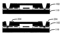
- FIGS. 2A-2B demonstrate interconnection of through-wafer vias in accordance with an embodiment of the present invention.
- FIG. 2A shows a cross-sectional view of a capped or stacked wafer device in which one or more bridge structures 202 are formed between the through-hole via 104 in the cap wafer 102 and the component 112 on the device wafer 110 .
- the bridge structures 202 can be formed on either the cap wafer 102 or the device wafer 110 .
- the bridge structures 202 are typically formed from a compliant material that allows for formation of the interconnection.
- the bridge structures 202 preferably jut out into the path between the through-hole via 104 and the component 112 in order to provide a contiguous exposed surface on which to grow an interconnection.
- FIG. 1 shows a cross-sectional view of a capped or stacked wafer device in which one or more bridge structures 202 are formed between the through-hole via 104 in the cap wafer 102 and the component 112 on the device wafer 110
- FIG. 2B shows an interconnection 204 that is formed through the through-hole via 104 to the component 112 across the bridge structures 202 . Because the interconnection 204 does not need to be built up across the entire gap, production time and cost can be significantly reduced. After the interconnections have been formed across the bridge structures, the bridge structures could be removed if necessary or desirable for a particular application.
- the bridge structures can be formed on either the cap wafer or the device wafer, it is typical for the bridge structures to be formed on the cap wafer.
- the bridge structures may be formed from the same material as the bonding material (e.g., a glass frit material), in which case the bridge structures may be formed at the same time the bonding material is formed.
- the bridge structures can serve as the bonding material and therefore separate bonding structures may be optional.
- the bridge structures can be formed using any of a variety of materials and techniques, and the present invention is not limited to any particular materials or techniques. Two exemplary techniques for forming bridge structures are described below.
- FIGS. 3A-3E demonstrate a first technique for forming bridge structures in which the bridge structures are deposited on the cap wafer, in accordance with an embodiment of the present invention.
- FIG. 3A shows an essentially blank cap wafer 102 .
- FIG. 3B shows the cap wafer 102 after formation of through-hole vias 104 and cavity 108 .
- FIG. 3C shows the cap wafer 102 after formation of bonding materials 106 and bridge structures 202 . It should be noted that the bonding materials 106 and bridge structures 202 can be fabricated from the same material or different materials and using the same process or different processes.
- FIG. 3A shows an essentially blank cap wafer 102 .
- FIG. 3B shows the cap wafer 102 after formation of through-hole vias 104 and cavity 108 .
- FIG. 3C shows the cap wafer 102 after formation of bonding materials 106 and bridge structures 202 .
- the bonding materials 106 and bridge structures 202 can be fabricated from the same material or different materials and using
- FIG. 3D shows the cap wafer 102 bonded to a device wafer 110 , with the bridge structures 202 spanning the gap between the through-hole vias 104 and components on the device wafer 110 .
- FIG. 3E shows interconnections 204 that are formed through the through-hole vias to the components across the bridge structures.
- the bridge structures 202 may be fabricated to the edge of the through-hole vias rather than jutting out past the edge of the through-hole vias.
- the bridge structures 202 may be compressed and therefore expand so as to jut out past the edge of the through-hole vias.
- the bridge structures 202 jut out into the path between the through-hole vias and the components in order to provide contiguous exposed surfaces on which to grow interconnections.
- FIGS. 4A-4F demonstrate a second technique for forming bridge structures in which the bridge structures are etched on the cap wafer, in accordance with an embodiment of the present invention.
- FIG. 4A shows a cap wafer 102 having a deposited bonding/bridge material layer 402 .
- FIG. 4B shows the cap wafer 102 after formation of through-hole vias 104 .
- FIG. 4C shows the cap wafer 102 after etching of the bonding/bridge material layer to expose the through-hole vias 104 and form the bonding materials 106 and bridge structures 202 .
- FIG. 4D shows the cap wafer 102 after forming cavity 108 .
- FIG. 4A shows a cap wafer 102 having a deposited bonding/bridge material layer 402 .
- FIG. 4B shows the cap wafer 102 after formation of through-hole vias 104 .
- FIG. 4C shows the cap wafer 102 after etching of the bonding/bridge material layer to expose the through-hole vias
- FIG. 4E shows the cap wafer 102 bonded to a device wafer 110 , with the bridge structures 202 spanning the gap between the through-hole vias 104 and components on the device wafer 110 .
- FIG. 4F shows interconnections 204 that are formed through the through-hole vias to the components across the bridge structures.
- the bridge structures 202 may be fabricated beyond the edge of the through-hole vias so as to jut out past the edge of the through-hole vias.
- the bridge structures 202 jut out into the path between the through-hole vias and the components in order to provide contiguous exposed surfaces on which to grow interconnections.
- FIGS. 5A-5D demonstrate some exemplary bridge structure configurations in accordance with embodiments of the present invention.
- FIG. 5A shows a ring-shaped bridge structure 502 surrounding the through-hole via (represented by the inner circle 503 ).
- FIG. 5B shows two rectangular-shaped bridge structures 504 flanking a through-hole via 505 .
- FIG. 5C shows multiple bridge structure 506 adjacent to multiple through-hole vias 507 .
- FIG. 5D shows a single elongated bridge structure 508 adjacent to multiple through-hole vias 509 .
- the present invention is in no way limited to these or to any particular bridge structure shapes or configurations.
- bridge structures can be formed on the cap wafer and/or the device wafer using any of a variety of techniques, and the present invention is not limited to any particular technique or techniques for forming the bridge structures.
- bridge structures can be formed using a material deposition process, such as screen printing, shadow masking, physical vapor deposition (e.g., evaporation or sputtering), or chemical vapor deposition, to name but a few.
- interconnections can be formed through the through-hole via using any of a variety of techniques, and the present invention is not limited to any particular technique or techniques for forming the interconnections.
- interconnections can be formed using a material deposition process, such as screen printing, shadow masking, physical vapor deposition (e.g., evaporation or sputtering), or chemical vapor deposition, to name but a few.
- the bridge structures are generally shown to contact the components on the device wafer, the bridge structures are not required to contact the components on the device wafer, although it is preferable that the bridge structures at least abut the components. In situations where the bridge structures do not abut or otherwise contact the components, any surface material between the edge of the bridge structures and the components should allow for formation of the interconnections.
- the present invention is in no way limited to the shape of the through-hole vias.
- the through-hole vias could have square openings, and the sides of the through-hole vias could be sloped or unsloped.
- the through-hole vias are typically fabricated by etching, although the through-hole vias can be formed in other ways, and the present invention is not limited to any particular way of forming the through-hole vias.
- the cap wafer and/or the device wafer can be based on any of a variety of substrates, including, but in no way limited to, silicon, polysilicon, glass, ceramic, or metal substrates, to name but a few. If the cap wafer is made from an electrically conductive material (e.g., silicon, which is semiconducting, or metal, which is conducting), then the through-hole vias must typically be coated or lined with an insulating material (e.g., an oxide or other insulating material) before an electrical interconnection is formed through the through-hole via. For convenience, such coated or lined through-hole vias are not shown in the drawings.
- an electrically conductive material e.g., silicon, which is semiconducting, or metal, which is conducting
- an insulating material e.g., an oxide or other insulating material
- the cap wafer includes a cavity to fit around a corresponding structure on the device wafer.
- This cavity should be considered an optional feature and may not be required in all embodiments. Therefore, the present invention does not require formation of a cavity in the cap wafer.
Abstract
Description
Claims (20)
Priority Applications (1)
| Application Number | Priority Date | Filing Date | Title |
|---|---|---|---|
| US11/043,580 US7608534B2 (en) | 2004-06-02 | 2005-01-26 | Interconnection of through-wafer vias using bridge structures |
Applications Claiming Priority (2)
| Application Number | Priority Date | Filing Date | Title |
|---|---|---|---|
| US57620504P | 2004-06-02 | 2004-06-02 | |
| US11/043,580 US7608534B2 (en) | 2004-06-02 | 2005-01-26 | Interconnection of through-wafer vias using bridge structures |
Publications (2)
| Publication Number | Publication Date |
|---|---|
| US20060166480A1 US20060166480A1 (en) | 2006-07-27 |
| US7608534B2 true US7608534B2 (en) | 2009-10-27 |
Family
ID=36697405
Family Applications (1)
| Application Number | Title | Priority Date | Filing Date |
|---|---|---|---|
| US11/043,580 Active 2025-11-16 US7608534B2 (en) | 2004-06-02 | 2005-01-26 | Interconnection of through-wafer vias using bridge structures |
Country Status (1)
| Country | Link |
|---|---|
| US (1) | US7608534B2 (en) |
Cited By (9)
| Publication number | Priority date | Publication date | Assignee | Title |
|---|---|---|---|---|
| US8492260B2 (en) | 2010-08-30 | 2013-07-23 | Semionductor Components Industries, LLC | Processes of forming an electronic device including a feature in a trench |
| US8653634B2 (en) | 2012-06-11 | 2014-02-18 | Advanced Semiconductor Engineering, Inc. | EMI-shielded semiconductor devices and methods of making |
| US8963316B2 (en) | 2012-02-15 | 2015-02-24 | Advanced Semiconductor Engineering, Inc. | Semiconductor device and method for manufacturing the same |
| US8981533B2 (en) | 2012-09-13 | 2015-03-17 | Semiconductor Components Industries, Llc | Electronic device including a via and a conductive structure, a process of forming the same, and an interposer |
| US9812354B2 (en) | 2015-05-15 | 2017-11-07 | Semiconductor Components Industries, Llc | Process of forming an electronic device including a material defining a void |
| CN109835870A (en) * | 2019-02-19 | 2019-06-04 | 厦门大学 | A kind of integrated encapsulation method and structure of MEMS device and ASIC processing circuit IC |
| US10453787B2 (en) | 2015-05-21 | 2019-10-22 | The Charles Stark Draper Laboratory, Inc. | Method and apparatus for forming multi-layered vias in sequentially fabricated circuits |
| US20200130012A1 (en) * | 2018-10-25 | 2020-04-30 | Texas Instruments Incorporated | Broadband ultrasound transducers and related methods |
| US11501928B2 (en) | 2020-03-27 | 2022-11-15 | Menlo Microsystems, Inc. | MEMS device built on substrate with ruthenium based contact surface material |
Families Citing this family (8)
| Publication number | Priority date | Publication date | Assignee | Title |
|---|---|---|---|---|
| US8143095B2 (en) * | 2005-03-22 | 2012-03-27 | Tessera, Inc. | Sequential fabrication of vertical conductive interconnects in capped chips |
| US20070170528A1 (en) * | 2006-01-20 | 2007-07-26 | Aaron Partridge | Wafer encapsulated microelectromechanical structure and method of manufacturing same |
| US7936062B2 (en) | 2006-01-23 | 2011-05-03 | Tessera Technologies Ireland Limited | Wafer level chip packaging |
| US8604605B2 (en) | 2007-01-05 | 2013-12-10 | Invensas Corp. | Microelectronic assembly with multi-layer support structure |
| JP5330697B2 (en) * | 2007-03-19 | 2013-10-30 | 株式会社リコー | Functional element package and manufacturing method thereof |
| KR100872404B1 (en) | 2007-04-26 | 2008-12-05 | (주) 파이오닉스 | Wafer bonding packaging method |
| US20100037933A1 (en) | 2008-08-12 | 2010-02-18 | Harold John Hovel | Solar cell panels and method of fabricating same |
| NL2009757C2 (en) * | 2012-11-05 | 2014-05-08 | Micronit Microfluidics Bv | Method for forming an electrically conductive via in a substrate. |
Citations (84)
| Publication number | Priority date | Publication date | Assignee | Title |
|---|---|---|---|---|
| US4499655A (en) | 1981-03-18 | 1985-02-19 | General Electric Company | Method for making alignment-enhancing feed-through conductors for stackable silicon-on-sapphire |
| US4921157A (en) | 1989-03-15 | 1990-05-01 | Microelectronics Center Of North Carolina | Fluxless soldering process |
| US5089880A (en) | 1989-06-07 | 1992-02-18 | Amdahl Corporation | Pressurized interconnection system for semiconductor chips |
| US5229647A (en) | 1991-03-27 | 1993-07-20 | Micron Technology, Inc. | High density data storage using stacked wafers |
| US5314572A (en) | 1990-08-17 | 1994-05-24 | Analog Devices, Inc. | Method for fabricating microstructures |
| US5326726A (en) | 1990-08-17 | 1994-07-05 | Analog Devices, Inc. | Method for fabricating monolithic chip containing integrated circuitry and suspended microstructure |
| US5345824A (en) | 1990-08-17 | 1994-09-13 | Analog Devices, Inc. | Monolithic accelerometer |
| US5355022A (en) | 1991-09-10 | 1994-10-11 | Mitsubishi Denki Kabushiki Kaisha | Stacked-type semiconductor device |
| US5417111A (en) | 1990-08-17 | 1995-05-23 | Analog Devices, Inc. | Monolithic chip containing integrated circuitry and suspended microstructure |
| US5511428A (en) | 1994-06-10 | 1996-04-30 | Massachusetts Institute Of Technology | Backside contact of sensor microstructures |
| WO1996013062A1 (en) | 1994-10-19 | 1996-05-02 | Ceram Incorporated | Apparatus and method of manufacturing stacked wafer array |
| US5545912A (en) | 1994-10-27 | 1996-08-13 | Motorola, Inc. | Electronic device enclosure including a conductive cap and substrate |
| US5610431A (en) | 1995-05-12 | 1997-03-11 | The Charles Stark Draper Laboratory, Inc. | Covers for micromechanical sensors and other semiconductor devices |
| US5620931A (en) | 1990-08-17 | 1997-04-15 | Analog Devices, Inc. | Methods for fabricating monolithic device containing circuitry and suspended microstructure |
| EP0851492A2 (en) | 1996-12-06 | 1998-07-01 | Texas Instruments Incorporated | Surface-mounted substrate structure and method |
| US5872496A (en) | 1993-12-20 | 1999-02-16 | The Nippon Signal Co., Ltd. | Planar type electromagnetic relay and method of manufacturing thereof |
| US5929497A (en) | 1998-06-11 | 1999-07-27 | Delco Electronics Corporation | Batch processed multi-lead vacuum packaging for integrated sensors and circuits |
| US5939633A (en) | 1997-06-18 | 1999-08-17 | Analog Devices, Inc. | Apparatus and method for multi-axis capacitive sensing |
| US6071389A (en) | 1998-08-21 | 2000-06-06 | Tosoh Smd, Inc. | Diffusion bonded sputter target assembly and method of making |
| US6087719A (en) | 1997-04-25 | 2000-07-11 | Kabushiki Kaisha Toshiba | Chip for multi-chip semiconductor device and method of manufacturing the same |
| US6118181A (en) | 1998-07-29 | 2000-09-12 | Agilent Technologies, Inc. | System and method for bonding wafers |
| US6153839A (en) | 1998-10-22 | 2000-11-28 | Northeastern University | Micromechanical switching devices |
| US6236115B1 (en) | 1995-12-27 | 2001-05-22 | International Business Machines Corporation | High density integrated circuit packaging with chip stacking and via interconnections |
| US6239495B1 (en) | 1998-07-29 | 2001-05-29 | Kabushiki Kaisha Toshiba | Multichip semiconductor device and memory card |
| WO2001056921A2 (en) | 2000-02-02 | 2001-08-09 | Raytheon Company | Vacuum package fabrication of microelectromechanical system devices with integrated circuit components |
| US6297072B1 (en) | 1998-04-17 | 2001-10-02 | Interuniversitair Micro-Elktronica Centrum (Imec Vzw) | Method of fabrication of a microstructure having an internal cavity |
| US20010028114A1 (en) | 2000-03-27 | 2001-10-11 | Kabushiki Kaisha Toshiba | Semiconductor device including memory unit and semiconductor module including memory units |
| US6303986B1 (en) | 1998-07-29 | 2001-10-16 | Silicon Light Machines | Method of and apparatus for sealing an hermetic lid to a semiconductor die |
| US6307169B1 (en) | 2000-02-01 | 2001-10-23 | Motorola Inc. | Micro-electromechanical switch |
| US6323550B1 (en) | 1995-06-06 | 2001-11-27 | Analog Devices, Inc. | Package for sealing an integrated circuit die |
| US6335224B1 (en) | 2000-05-16 | 2002-01-01 | Sandia Corporation | Protection of microelectronic devices during packaging |
| US6365975B1 (en) | 1997-04-02 | 2002-04-02 | Tessera, Inc. | Chip with internal signal routing in external element |
| US6384353B1 (en) | 2000-02-01 | 2002-05-07 | Motorola, Inc. | Micro-electromechanical system device |
| US20020056925A1 (en) | 1997-07-10 | 2002-05-16 | Kang Sung Kwon | Interconnections with electrically conductive adhesives: structures, materials, method and their applications |
| US6406934B1 (en) | 2000-09-05 | 2002-06-18 | Amkor Technology, Inc. | Wafer level production of chip size semiconductor packages |
| EP1219565A1 (en) | 2000-12-29 | 2002-07-03 | STMicroelectronics S.r.l. | Process for manufacturing integrated devices having connections on separate wafers and stacking the same |
| US6429511B2 (en) | 1999-07-23 | 2002-08-06 | Agilent Technologies, Inc. | Microcap wafer-level package |
| US6433411B1 (en) | 2000-05-22 | 2002-08-13 | Agere Systems Guardian Corp. | Packaging micromechanical devices |
| US6436853B2 (en) | 1998-12-03 | 2002-08-20 | University Of Michigan | Microstructures |
| US6448109B1 (en) | 2000-11-15 | 2002-09-10 | Analog Devices, Inc. | Wafer level method of capping multiple MEMS elements |
| US6448622B1 (en) | 1999-01-15 | 2002-09-10 | The Regents Of The University Of California | Polycrystalline silicon-germanium films for micro-electromechanical systems application |
| US6452238B1 (en) | 1999-10-04 | 2002-09-17 | Texas Instruments Incorporated | MEMS wafer level package |
| WO2002093122A2 (en) | 2001-05-11 | 2002-11-21 | Robert Bosch Gmbh | Sensor arrangement, in particular micro-mechanical sensor arrangement |
| US6504253B2 (en) | 2000-04-28 | 2003-01-07 | Stmicroelectronics S.R.L. | Structure for electrically connecting a first body of semiconductor material overlaid by a second body of semiconductor material composite structure using electric connection structure |
| US6505511B1 (en) | 1997-09-02 | 2003-01-14 | Analog Devices, Inc. | Micromachined gyros |
| US6512300B2 (en) * | 2001-01-10 | 2003-01-28 | Raytheon Company | Water level interconnection |
| US20030038327A1 (en) | 2001-08-24 | 2003-02-27 | Honeywell International, Inc. | Hermetically sealed silicon micro-machined electromechanical system (MEMS) device having diffused conductors |
| EP1296374A1 (en) | 2001-09-14 | 2003-03-26 | STMicroelectronics S.r.l. | Process for bonding and electrically connecting microsystems integrated in several distinct substrates |
| US6548391B1 (en) | 1999-05-27 | 2003-04-15 | Fraunhofer-Gesellschaft Zur Foerderung Der Angewandten Forschung E. V. | Method of vertically integrating electric components by means of back contacting |
| US6559530B2 (en) | 2001-09-19 | 2003-05-06 | Raytheon Company | Method of integrating MEMS device with low-resistivity silicon substrates |
| US6577013B1 (en) | 2000-09-05 | 2003-06-10 | Amkor Technology, Inc. | Chip size semiconductor packages with stacked dies |
| US6621168B2 (en) | 2000-12-28 | 2003-09-16 | Intel Corporation | Interconnected circuit board assembly and system |
| US6625367B2 (en) | 2000-08-21 | 2003-09-23 | Triquint Technology Holding Co. | Optoelectronic device having a P-contact and an N-contact located over a same side of a substrate and a method of manufacture therefor |
| US6630725B1 (en) | 2000-10-06 | 2003-10-07 | Motorola, Inc. | Electronic component and method of manufacture |
| US20040016989A1 (en) | 2000-10-12 | 2004-01-29 | Qing Ma | MEMS device integrated chip package, and method of making same |
| US6686642B2 (en) | 2001-06-11 | 2004-02-03 | Hewlett-Packard Development Company, L.P. | Multi-level integrated circuit for wide-gap substrate bonding |
| US20040077154A1 (en) | 2002-10-17 | 2004-04-22 | Ranganathan Nagarajan | Wafer-level package for micro-electro-mechanical systems |
| US20040077117A1 (en) * | 2002-10-18 | 2004-04-22 | Xiaoyi Ding | Feedthrough design and method for a hermetically sealed microdevice |
| US6744127B2 (en) | 2001-05-31 | 2004-06-01 | Infineon Technologies Ag | Semiconductor chip, memory module and method for testing the semiconductor chip |
| US6753208B1 (en) | 1998-03-20 | 2004-06-22 | Mcsp, Llc | Wafer scale method of packaging integrated circuit die |
| US20040157407A1 (en) | 2003-02-07 | 2004-08-12 | Ziptronix | Room temperature metal direct bonding |
| US6781239B1 (en) | 2001-12-05 | 2004-08-24 | National Semiconductor Corporation | Integrated circuit and method of forming the integrated circuit having a die with high Q inductors and capacitors attached to a die with a circuit as a flip chip |
| US6791193B2 (en) | 2002-03-08 | 2004-09-14 | Kabushiki Kaisha Toshiba | Chip mounting substrate, first level assembly, and second level assembly |
| US20040219763A1 (en) | 2002-02-20 | 2004-11-04 | Kim Sarah E. | Process of vertically stacking multiple wafers supporting different active integrated circuit (IC) devices |
| US20050003652A1 (en) | 2003-07-02 | 2005-01-06 | Shriram Ramanathan | Method and apparatus for low temperature copper to copper bonding |
| US6853067B1 (en) | 1999-10-12 | 2005-02-08 | Microassembly Technologies, Inc. | Microelectromechanical systems using thermocompression bonding |
| US6852926B2 (en) | 2002-03-26 | 2005-02-08 | Intel Corporation | Packaging microelectromechanical structures |
| US20050104228A1 (en) | 2003-11-13 | 2005-05-19 | Rigg Sidney B. | Microelectronic devices, methods for forming vias in microelectronic devices, and methods for packaging microelectronic devices |
| US20050104187A1 (en) | 2003-10-31 | 2005-05-19 | Polsky Cynthia H. | Redistribution of substrate interconnects |
| US6909146B1 (en) | 1992-02-12 | 2005-06-21 | Intersil Corporation | Bonded wafer with metal silicidation |
| US6911727B1 (en) | 1995-06-06 | 2005-06-28 | Analog Devices, Inc. | Package for sealing an integrated circuit die |
| WO2005058749A1 (en) | 2003-12-15 | 2005-06-30 | Analog Devices, Inc. | Semiconductor assembly with conductive rim and method of producing the same |
| US20050170609A1 (en) * | 2003-12-15 | 2005-08-04 | Alie Susan A. | Conductive bond for through-wafer interconnect |
| US6933163B2 (en) * | 2002-09-27 | 2005-08-23 | Analog Devices, Inc. | Fabricating integrated micro-electromechanical systems using an intermediate electrode layer |
| US20050186705A1 (en) | 2002-07-31 | 2005-08-25 | Jackson Timothy L. | Semiconductor dice having backside redistribution layer accessed using through-silicon vias, methods |
| US6936918B2 (en) | 2003-12-15 | 2005-08-30 | Analog Devices, Inc. | MEMS device with conductive path through substrate |
| US6940636B2 (en) | 2001-09-20 | 2005-09-06 | Analog Devices, Inc. | Optical switching apparatus and method of assembling same |
| US6964882B2 (en) | 2002-09-27 | 2005-11-15 | Analog Devices, Inc. | Fabricating complex micro-electromechanical systems using a flip bonding technique |
| US20060046475A1 (en) | 2004-09-02 | 2006-03-02 | Wark James M | Sloped vias in a substrate, spring-like deflecting contacts, and methods of making |
| US20060043569A1 (en) | 2004-08-27 | 2006-03-02 | Benson Peter A | Low temperature methods of forming back side redistribution layers in association with through wafer interconnects, semiconductor devices including same, and assemblies |
| JP2006186179A (en) | 2004-12-28 | 2006-07-13 | Matsushita Electric Ind Co Ltd | Electronic component compression bonding device, electronic component compression bonding inspecting device, and electronic component compression bonding inspection method |
| US20070069391A1 (en) | 2005-09-27 | 2007-03-29 | Stmicroelectronics S.R.I. | Stacked die semiconductor package |
| US7275424B2 (en) * | 2003-09-08 | 2007-10-02 | Analog Devices, Inc. | Wafer level capped sensor |
| US7291925B2 (en) | 2004-11-16 | 2007-11-06 | Samsung Electronics Co., Ltd. | Stack package using anisotropic conductive film (ACF) and method of making same |
-
2005
- 2005-01-26 US US11/043,580 patent/US7608534B2/en active Active
Patent Citations (95)
| Publication number | Priority date | Publication date | Assignee | Title |
|---|---|---|---|---|
| US4499655A (en) | 1981-03-18 | 1985-02-19 | General Electric Company | Method for making alignment-enhancing feed-through conductors for stackable silicon-on-sapphire |
| US4921157A (en) | 1989-03-15 | 1990-05-01 | Microelectronics Center Of North Carolina | Fluxless soldering process |
| US5089880A (en) | 1989-06-07 | 1992-02-18 | Amdahl Corporation | Pressurized interconnection system for semiconductor chips |
| US5345824A (en) | 1990-08-17 | 1994-09-13 | Analog Devices, Inc. | Monolithic accelerometer |
| US5314572A (en) | 1990-08-17 | 1994-05-24 | Analog Devices, Inc. | Method for fabricating microstructures |
| US5326726A (en) | 1990-08-17 | 1994-07-05 | Analog Devices, Inc. | Method for fabricating monolithic chip containing integrated circuitry and suspended microstructure |
| US5620931A (en) | 1990-08-17 | 1997-04-15 | Analog Devices, Inc. | Methods for fabricating monolithic device containing circuitry and suspended microstructure |
| US5417111A (en) | 1990-08-17 | 1995-05-23 | Analog Devices, Inc. | Monolithic chip containing integrated circuitry and suspended microstructure |
| US5540095A (en) | 1990-08-17 | 1996-07-30 | Analog Devices, Inc. | Monolithic accelerometer |
| US5229647A (en) | 1991-03-27 | 1993-07-20 | Micron Technology, Inc. | High density data storage using stacked wafers |
| US5355022A (en) | 1991-09-10 | 1994-10-11 | Mitsubishi Denki Kabushiki Kaisha | Stacked-type semiconductor device |
| US6909146B1 (en) | 1992-02-12 | 2005-06-21 | Intersil Corporation | Bonded wafer with metal silicidation |
| US5872496A (en) | 1993-12-20 | 1999-02-16 | The Nippon Signal Co., Ltd. | Planar type electromagnetic relay and method of manufacturing thereof |
| US5511428A (en) | 1994-06-10 | 1996-04-30 | Massachusetts Institute Of Technology | Backside contact of sensor microstructures |
| WO1996013062A1 (en) | 1994-10-19 | 1996-05-02 | Ceram Incorporated | Apparatus and method of manufacturing stacked wafer array |
| US5545912A (en) | 1994-10-27 | 1996-08-13 | Motorola, Inc. | Electronic device enclosure including a conductive cap and substrate |
| US5610431A (en) | 1995-05-12 | 1997-03-11 | The Charles Stark Draper Laboratory, Inc. | Covers for micromechanical sensors and other semiconductor devices |
| US20050269678A1 (en) | 1995-06-06 | 2005-12-08 | Martin John R | Package for sealing an integrated circuit die |
| US6911727B1 (en) | 1995-06-06 | 2005-06-28 | Analog Devices, Inc. | Package for sealing an integrated circuit die |
| US6323550B1 (en) | 1995-06-06 | 2001-11-27 | Analog Devices, Inc. | Package for sealing an integrated circuit die |
| US6236115B1 (en) | 1995-12-27 | 2001-05-22 | International Business Machines Corporation | High density integrated circuit packaging with chip stacking and via interconnections |
| EP0851492A2 (en) | 1996-12-06 | 1998-07-01 | Texas Instruments Incorporated | Surface-mounted substrate structure and method |
| US6365975B1 (en) | 1997-04-02 | 2002-04-02 | Tessera, Inc. | Chip with internal signal routing in external element |
| US6087719A (en) | 1997-04-25 | 2000-07-11 | Kabushiki Kaisha Toshiba | Chip for multi-chip semiconductor device and method of manufacturing the same |
| US5939633A (en) | 1997-06-18 | 1999-08-17 | Analog Devices, Inc. | Apparatus and method for multi-axis capacitive sensing |
| US20020056925A1 (en) | 1997-07-10 | 2002-05-16 | Kang Sung Kwon | Interconnections with electrically conductive adhesives: structures, materials, method and their applications |
| US6505511B1 (en) | 1997-09-02 | 2003-01-14 | Analog Devices, Inc. | Micromachined gyros |
| US6753208B1 (en) | 1998-03-20 | 2004-06-22 | Mcsp, Llc | Wafer scale method of packaging integrated circuit die |
| US6297072B1 (en) | 1998-04-17 | 2001-10-02 | Interuniversitair Micro-Elktronica Centrum (Imec Vzw) | Method of fabrication of a microstructure having an internal cavity |
| US5929497A (en) | 1998-06-11 | 1999-07-27 | Delco Electronics Corporation | Batch processed multi-lead vacuum packaging for integrated sensors and circuits |
| US6118181A (en) | 1998-07-29 | 2000-09-12 | Agilent Technologies, Inc. | System and method for bonding wafers |
| US6239495B1 (en) | 1998-07-29 | 2001-05-29 | Kabushiki Kaisha Toshiba | Multichip semiconductor device and memory card |
| US6303986B1 (en) | 1998-07-29 | 2001-10-16 | Silicon Light Machines | Method of and apparatus for sealing an hermetic lid to a semiconductor die |
| US6071389A (en) | 1998-08-21 | 2000-06-06 | Tosoh Smd, Inc. | Diffusion bonded sputter target assembly and method of making |
| US6153839A (en) | 1998-10-22 | 2000-11-28 | Northeastern University | Micromechanical switching devices |
| US6436853B2 (en) | 1998-12-03 | 2002-08-20 | University Of Michigan | Microstructures |
| US6448622B1 (en) | 1999-01-15 | 2002-09-10 | The Regents Of The University Of California | Polycrystalline silicon-germanium films for micro-electromechanical systems application |
| US6548391B1 (en) | 1999-05-27 | 2003-04-15 | Fraunhofer-Gesellschaft Zur Foerderung Der Angewandten Forschung E. V. | Method of vertically integrating electric components by means of back contacting |
| US6429511B2 (en) | 1999-07-23 | 2002-08-06 | Agilent Technologies, Inc. | Microcap wafer-level package |
| US6452238B1 (en) | 1999-10-04 | 2002-09-17 | Texas Instruments Incorporated | MEMS wafer level package |
| US6743656B2 (en) * | 1999-10-04 | 2004-06-01 | Texas Instruments Incorporated | MEMS wafer level package |
| US6853067B1 (en) | 1999-10-12 | 2005-02-08 | Microassembly Technologies, Inc. | Microelectromechanical systems using thermocompression bonding |
| US6384353B1 (en) | 2000-02-01 | 2002-05-07 | Motorola, Inc. | Micro-electromechanical system device |
| US6307169B1 (en) | 2000-02-01 | 2001-10-23 | Motorola Inc. | Micro-electromechanical switch |
| WO2001056921A2 (en) | 2000-02-02 | 2001-08-09 | Raytheon Company | Vacuum package fabrication of microelectromechanical system devices with integrated circuit components |
| US20010028114A1 (en) | 2000-03-27 | 2001-10-11 | Kabushiki Kaisha Toshiba | Semiconductor device including memory unit and semiconductor module including memory units |
| US6504253B2 (en) | 2000-04-28 | 2003-01-07 | Stmicroelectronics S.R.L. | Structure for electrically connecting a first body of semiconductor material overlaid by a second body of semiconductor material composite structure using electric connection structure |
| US6335224B1 (en) | 2000-05-16 | 2002-01-01 | Sandia Corporation | Protection of microelectronic devices during packaging |
| US6433411B1 (en) | 2000-05-22 | 2002-08-13 | Agere Systems Guardian Corp. | Packaging micromechanical devices |
| US6625367B2 (en) | 2000-08-21 | 2003-09-23 | Triquint Technology Holding Co. | Optoelectronic device having a P-contact and an N-contact located over a same side of a substrate and a method of manufacture therefor |
| US6406934B1 (en) | 2000-09-05 | 2002-06-18 | Amkor Technology, Inc. | Wafer level production of chip size semiconductor packages |
| US6577013B1 (en) | 2000-09-05 | 2003-06-10 | Amkor Technology, Inc. | Chip size semiconductor packages with stacked dies |
| US6630725B1 (en) | 2000-10-06 | 2003-10-07 | Motorola, Inc. | Electronic component and method of manufacture |
| US7291561B2 (en) | 2000-10-12 | 2007-11-06 | Intel Corporation | MEMS device integrated chip package, and method of making same |
| US20040016989A1 (en) | 2000-10-12 | 2004-01-29 | Qing Ma | MEMS device integrated chip package, and method of making same |
| US6448109B1 (en) | 2000-11-15 | 2002-09-10 | Analog Devices, Inc. | Wafer level method of capping multiple MEMS elements |
| US6621168B2 (en) | 2000-12-28 | 2003-09-16 | Intel Corporation | Interconnected circuit board assembly and system |
| EP1219565A1 (en) | 2000-12-29 | 2002-07-03 | STMicroelectronics S.r.l. | Process for manufacturing integrated devices having connections on separate wafers and stacking the same |
| US6512300B2 (en) * | 2001-01-10 | 2003-01-28 | Raytheon Company | Water level interconnection |
| US6633079B2 (en) | 2001-01-10 | 2003-10-14 | Raytheon Company | Wafer level interconnection |
| US20040232500A1 (en) | 2001-05-11 | 2004-11-25 | Joachim Rudhard | Sensor arrangement,in particular a micro-mechanical sensor arrangement |
| US7334491B2 (en) | 2001-05-11 | 2008-02-26 | Robert Bosch Gmbh | Sensor arrangement, in particular a micro-mechanical sensor arrangement |
| WO2002093122A2 (en) | 2001-05-11 | 2002-11-21 | Robert Bosch Gmbh | Sensor arrangement, in particular micro-mechanical sensor arrangement |
| US6744127B2 (en) | 2001-05-31 | 2004-06-01 | Infineon Technologies Ag | Semiconductor chip, memory module and method for testing the semiconductor chip |
| US6686642B2 (en) | 2001-06-11 | 2004-02-03 | Hewlett-Packard Development Company, L.P. | Multi-level integrated circuit for wide-gap substrate bonding |
| US20030038327A1 (en) | 2001-08-24 | 2003-02-27 | Honeywell International, Inc. | Hermetically sealed silicon micro-machined electromechanical system (MEMS) device having diffused conductors |
| US6906395B2 (en) | 2001-08-24 | 2005-06-14 | Honeywell International, Inc. | Hermetically sealed silicon micro-machined electromechanical system (MEMS) device having diffused conductors |
| EP1296374A1 (en) | 2001-09-14 | 2003-03-26 | STMicroelectronics S.r.l. | Process for bonding and electrically connecting microsystems integrated in several distinct substrates |
| US6559530B2 (en) | 2001-09-19 | 2003-05-06 | Raytheon Company | Method of integrating MEMS device with low-resistivity silicon substrates |
| US6940636B2 (en) | 2001-09-20 | 2005-09-06 | Analog Devices, Inc. | Optical switching apparatus and method of assembling same |
| US6781239B1 (en) | 2001-12-05 | 2004-08-24 | National Semiconductor Corporation | Integrated circuit and method of forming the integrated circuit having a die with high Q inductors and capacitors attached to a die with a circuit as a flip chip |
| US20040219763A1 (en) | 2002-02-20 | 2004-11-04 | Kim Sarah E. | Process of vertically stacking multiple wafers supporting different active integrated circuit (IC) devices |
| US6791193B2 (en) | 2002-03-08 | 2004-09-14 | Kabushiki Kaisha Toshiba | Chip mounting substrate, first level assembly, and second level assembly |
| US6852926B2 (en) | 2002-03-26 | 2005-02-08 | Intel Corporation | Packaging microelectromechanical structures |
| US20050186705A1 (en) | 2002-07-31 | 2005-08-25 | Jackson Timothy L. | Semiconductor dice having backside redistribution layer accessed using through-silicon vias, methods |
| US6964882B2 (en) | 2002-09-27 | 2005-11-15 | Analog Devices, Inc. | Fabricating complex micro-electromechanical systems using a flip bonding technique |
| US6933163B2 (en) * | 2002-09-27 | 2005-08-23 | Analog Devices, Inc. | Fabricating integrated micro-electromechanical systems using an intermediate electrode layer |
| US20040077154A1 (en) | 2002-10-17 | 2004-04-22 | Ranganathan Nagarajan | Wafer-level package for micro-electro-mechanical systems |
| US20040077117A1 (en) * | 2002-10-18 | 2004-04-22 | Xiaoyi Ding | Feedthrough design and method for a hermetically sealed microdevice |
| US6962835B2 (en) | 2003-02-07 | 2005-11-08 | Ziptronix, Inc. | Method for room temperature metal direct bonding |
| US20040157407A1 (en) | 2003-02-07 | 2004-08-12 | Ziptronix | Room temperature metal direct bonding |
| US20050003652A1 (en) | 2003-07-02 | 2005-01-06 | Shriram Ramanathan | Method and apparatus for low temperature copper to copper bonding |
| US7275424B2 (en) * | 2003-09-08 | 2007-10-02 | Analog Devices, Inc. | Wafer level capped sensor |
| US20050104187A1 (en) | 2003-10-31 | 2005-05-19 | Polsky Cynthia H. | Redistribution of substrate interconnects |
| US20050104228A1 (en) | 2003-11-13 | 2005-05-19 | Rigg Sidney B. | Microelectronic devices, methods for forming vias in microelectronic devices, and methods for packaging microelectronic devices |
| US20050170609A1 (en) * | 2003-12-15 | 2005-08-04 | Alie Susan A. | Conductive bond for through-wafer interconnect |
| US7034393B2 (en) | 2003-12-15 | 2006-04-25 | Analog Devices, Inc. | Semiconductor assembly with conductive rim and method of producing the same |
| US20060118946A1 (en) | 2003-12-15 | 2006-06-08 | Alie Susan A | Semiconductor assembly with conductive rim and method of producing the same |
| US6936918B2 (en) | 2003-12-15 | 2005-08-30 | Analog Devices, Inc. | MEMS device with conductive path through substrate |
| WO2005058749A1 (en) | 2003-12-15 | 2005-06-30 | Analog Devices, Inc. | Semiconductor assembly with conductive rim and method of producing the same |
| US20060043569A1 (en) | 2004-08-27 | 2006-03-02 | Benson Peter A | Low temperature methods of forming back side redistribution layers in association with through wafer interconnects, semiconductor devices including same, and assemblies |
| US20060046475A1 (en) | 2004-09-02 | 2006-03-02 | Wark James M | Sloped vias in a substrate, spring-like deflecting contacts, and methods of making |
| US7291925B2 (en) | 2004-11-16 | 2007-11-06 | Samsung Electronics Co., Ltd. | Stack package using anisotropic conductive film (ACF) and method of making same |
| JP2006186179A (en) | 2004-12-28 | 2006-07-13 | Matsushita Electric Ind Co Ltd | Electronic component compression bonding device, electronic component compression bonding inspecting device, and electronic component compression bonding inspection method |
| US20070069391A1 (en) | 2005-09-27 | 2007-03-29 | Stmicroelectronics S.R.I. | Stacked die semiconductor package |
Non-Patent Citations (32)
| Title |
|---|
| A.R. Mirza, Ph.D., "One Micron Precision, Wafer-Level Aligned Bonding for Interconnect, MEMS and Packaging Applications," IEEE 2000 Electronic Components and Technology Conference, pp. 676-680. |
| Analia Iperione, Authorized Officer Invitation to Pay Additional Fees and, Where Applicable, Protest Fee; PCT/US2008/050941. |
| Ando et al., New Packaging Technology for SAW Device, Corporate Components Development Center, Doc. No. WA1-3, 403-406, 4 pages. |
| Authorized Officer Götz, A., International Search Report and the Written Opinion of the International Searching Authority, PCT/US2005/012939, Sep. 7, 2005, 12 pages. |
| Authorized Officer Götz. A, International Search Report, International Searching Authority, International Application No. PCT/US2004/041549, Mar. 14, 2005, 7 pages. |
| Authorized Officer Guido Ploner, International Search Report and the Written Opinion of the International Searching Authority, PCT/US2007/080045, Dec. 6, 2007, 13 pages. |
| Authorized Officer Mattias Ahlstedt, International Search Report and the Written Opinion of the International Searching Authority, PCT/US2006/003673, Oct. 9, 2006, 20 pages. |
| Boustedt et al., Flip Chip as an Enabler for MEMS Packaging, 2002 Electronic Components and Technology Conference, Apr. 2002, 124-128, 5 pages. |
| Calmes, S., et al., "High Integrated 2-D Capacitive Micromachined Ultrasonic Transducers," IEEE Ultrasonics Symposium, 1999, pp. 1163-1166. |
| Chavan et al., A Monolithic Fully-Integrated Vacuum-Sealed CMOS Pressure Sensor, 2000 IEEE, Doc. No. 0-7803-5273-4/00, pp. 341-346. |
| Cheng, C., et al., "An Efficient Electrical Addressing Method Using Through-Wafer Vias for Two-Dimensional Ultrasonic Arrays," IEEE Ultrasonics Symposium, 2000, pp. 1179-1182. |
| Database WPI, Thomson Scientific, London, GB, AN 2006-541950 XP002501240 English abstract may be related to Japanese published application 2006 186179 A. |
| Guoqiang Feng et al., "Through Wafer Via Technology for 3-D Packaging," 2005 IEEE, 2005 6th International Conference on Electronic Packaging Technology, 4 pages. |
| K. Boustedt et al. "Flip Chip as an Enabler for MEMS Packaging," IEEE 2002 Electronic Components and Technology Conference, pp. 124-128. |
| Karimy, M., Examiner U.S. Office Action, dated Dec. 2, 2008, filed Feb. 3, 2005, Application No. 11/050,469. |
| Martin, Wafer Capping of MEMS with Fab-Friendly Metals, Analog Devices Inc., MicroMachined Products Division, SPIE presentation, Jan. 19, 2007. |
| Mitsuo Umemoto et al., "High Performance Vertical Interconnection for High-Density 3D Chip Stacking Package," IEEE 2004 Electronic Components and Technology Conference, pp. 616-623. |
| Naotaka Tanaka et al., "Mechanical Effects of Copper Through-Vias in a 3D Die-Stacked Module," IEEE 2002 Electronic Components and Technology Conference, pp. 473-479. |
| Ok et al., Generic, Direct-Chip-Attach MEMS Packaging Design with High Density and Aspect Ratio through-Wafer Electrical Interconnect, 2002 Electronic Components and Technology Conference, Apr. 2002, 232-237, 6 pages. |
| Ok et al., High Density, High Aspect Ratio Through-Wafer Electrical Interconnect Vias for MEMS Packaging, 2003 IEEE Transactions on Advanced Packaging, vol. 26, No. 3, Doc. No. 1521-3323, Aug. 2003, 302-309, 8 pages. |
| Park et al., A Novel-Low-Loss Wafer-Level Packaging of the RF-MEMS Devices, 2002 IEEE, Doc. No. 0-7803-7185, Feb. 2002, 681-684, 4 pages. |
| Patent Office of the People's Republic of China, Notification of the First Office Action, Appl. No. 200510007914.1, Applicant: Analog Devices, Inc. Nov. 2, 2007. |
| Philippe Foussier, Authorized Officer International Search Report and Written Opinion, PCT/U52008/050941, dated Nov. 3, 2008. |
| Premachandran et al., A Novel Electrically Conductive Wafer Through Hole Fille Vias Interconnect for 3D MEMS Packaging, May 2003, 627-630, 4 pages. |
| Seeger et al., Fabrication challenges for next-generation devices: Microelectromechanical systems for radio-frequency wireless communications, 2003 Society of Photo-Optical Instrumentation Engineers, Jul. 2003, 169-177, 9 pages. |
| ShellBGA, Online , Dec. 2, 2002, 2 pages. |
| Teomim et al., An innovative approach to wafer-level MEMS packaging, Solid State Technology-semiconductor manufacturing and wafer fabrication, Dec. 2, 2002, 1-4, 4 pages. |
| U.S. Office Action dated Dec. 27, 2006, U.S. Appl. No. 11/043,580, filed Jan. 26, 2005, 10 pages. |
| U.S. Office Action dated Nov. 7, 2006, U.S. Appl. No. 11/248,006, filed Oct. 11, 2005, 11 pages. |
| Wolffenbuttel, Low-Temperature Intermediate Au-Si Wafer Bonding; Eutectic or Silicide Bond, Sensors and Actuators A 62 (1997) pp. 680-686. |
| Y. Tomita et al., Advanced Packaging Technologies on 3D Stacked LSI Utilizing the Micro Interconnections and the Layered Microthin Encapsulation, IEEE, May 29, 2001, pp. 347-355. |
| Ziptronix White Paper, MEMS: Mainstream Process Integration, Ziptronix, 7 pages. |
Cited By (11)
| Publication number | Priority date | Publication date | Assignee | Title |
|---|---|---|---|---|
| US8492260B2 (en) | 2010-08-30 | 2013-07-23 | Semionductor Components Industries, LLC | Processes of forming an electronic device including a feature in a trench |
| US9117802B2 (en) | 2010-08-30 | 2015-08-25 | Semiconductor Components Industries, Llc | Electronic device including a feature in an opening |
| US8963316B2 (en) | 2012-02-15 | 2015-02-24 | Advanced Semiconductor Engineering, Inc. | Semiconductor device and method for manufacturing the same |
| US8653634B2 (en) | 2012-06-11 | 2014-02-18 | Advanced Semiconductor Engineering, Inc. | EMI-shielded semiconductor devices and methods of making |
| US8981533B2 (en) | 2012-09-13 | 2015-03-17 | Semiconductor Components Industries, Llc | Electronic device including a via and a conductive structure, a process of forming the same, and an interposer |
| US9812354B2 (en) | 2015-05-15 | 2017-11-07 | Semiconductor Components Industries, Llc | Process of forming an electronic device including a material defining a void |
| US10453787B2 (en) | 2015-05-21 | 2019-10-22 | The Charles Stark Draper Laboratory, Inc. | Method and apparatus for forming multi-layered vias in sequentially fabricated circuits |
| US20200130012A1 (en) * | 2018-10-25 | 2020-04-30 | Texas Instruments Incorporated | Broadband ultrasound transducers and related methods |
| CN109835870A (en) * | 2019-02-19 | 2019-06-04 | 厦门大学 | A kind of integrated encapsulation method and structure of MEMS device and ASIC processing circuit IC |
| CN109835870B (en) * | 2019-02-19 | 2020-12-11 | 厦门大学 | Integrated packaging method and structure of MEMS device and ASIC processing circuit IC |
| US11501928B2 (en) | 2020-03-27 | 2022-11-15 | Menlo Microsystems, Inc. | MEMS device built on substrate with ruthenium based contact surface material |
Also Published As
| Publication number | Publication date |
|---|---|
| US20060166480A1 (en) | 2006-07-27 |
Similar Documents
| Publication | Publication Date | Title |
|---|---|---|
| US7608534B2 (en) | Interconnection of through-wafer vias using bridge structures | |
| KR100907514B1 (en) | Sensor device, sensor system and method of manufacturing the same | |
| CN102173375B (en) | Electronic device | |
| TWI387065B (en) | Electronic device packages and methods of formation | |
| US6225145B1 (en) | Method of fabricating vacuum micro-structure | |
| JP5610177B2 (en) | Functional device and manufacturing method thereof | |
| EP0937985A1 (en) | Acceleration sensor and method of producing the same | |
| US20070298542A1 (en) | Multiple internal seal ring micro-electro-mechanical system vacuum packaging method | |
| JP2003530234A (en) | Micromechanical structure element and corresponding manufacturing method | |
| KR101048085B1 (en) | Functional device package and manufacturing method thereof | |
| JP2006247833A (en) | Mems element package and its manufacturing method | |
| US6794958B2 (en) | Method of fabricating a semiconductor device and an apparatus embodying the method | |
| TWI652728B (en) | Epi-poly etch stop for out of plane spacer defined electrode | |
| US6368885B1 (en) | Method for manufacturing a micromechanical component | |
| US7705412B2 (en) | SOI substrate and semiconductor acceleration sensor using the same | |
| EP1199744B1 (en) | Microcap wafer-level package | |
| US7531424B1 (en) | Vacuum wafer-level packaging for SOI-MEMS devices | |
| JP2014205235A (en) | Functional device | |
| CN111591951B (en) | Ultrasonic sensor structure and manufacturing method thereof | |
| CN111725078B (en) | Semiconductor device having discharge path and method of manufacturing the same | |
| JP2007216309A (en) | Electronic device and its manufacturing method | |
| JP2005228863A (en) | Semiconductor device, manufacturing method thereof and sensor | |
| JP2010181243A (en) | Method of manufacturing capacitance-type dynamic quantity sensor | |
| US20220287187A1 (en) | Component and Method for Manufacturing a Component | |
| KR101756847B1 (en) | Wearable patch type hybrid substrate and a method for fabricating the same |
Legal Events
| Date | Code | Title | Description |
|---|---|---|---|
| AS | Assignment |
Owner name: ANALOG DEVICES, INC., MASSACHUSETTS Free format text: ASSIGNMENT OF ASSIGNORS INTEREST;ASSIGNORS:YUN, CHANGHAN;VILLARREAL, JAVIER;REEL/FRAME:016236/0009 Effective date: 20050125 |
|
| AS | Assignment |
Owner name: ANALOG DEVICES, INC., MASSACHUSETTS Free format text: ASSIGNMENT OF ASSIGNORS INTEREST;ASSIGNORS:YUN, CHANGHAN;KARPMAN, MAURICE S.;VILLARREAL, JAVIER;REEL/FRAME:016310/0925;SIGNING DATES FROM 20050510 TO 20050511 |
|
| STCF | Information on status: patent grant |
Free format text: PATENTED CASE |
|
| CC | Certificate of correction | ||
| FPAY | Fee payment |
Year of fee payment: 4 |
|
| FPAY | Fee payment |
Year of fee payment: 8 |
|
| MAFP | Maintenance fee payment |
Free format text: PAYMENT OF MAINTENANCE FEE, 12TH YEAR, LARGE ENTITY (ORIGINAL EVENT CODE: M1553); ENTITY STATUS OF PATENT OWNER: LARGE ENTITY Year of fee payment: 12 |