US7613402B2 - Duobinary receiver - Google Patents
Duobinary receiver Download PDFInfo
- Publication number
- US7613402B2 US7613402B2 US10/730,413 US73041303A US7613402B2 US 7613402 B2 US7613402 B2 US 7613402B2 US 73041303 A US73041303 A US 73041303A US 7613402 B2 US7613402 B2 US 7613402B2
- Authority
- US
- United States
- Prior art keywords
- signal
- optical
- sampling window
- waveforms
- electrical signal
- Prior art date
- Legal status (The legal status is an assumption and is not a legal conclusion. Google has not performed a legal analysis and makes no representation as to the accuracy of the status listed.)
- Expired - Fee Related, expires
Links
Images


Classifications
-
- H—ELECTRICITY
- H04—ELECTRIC COMMUNICATION TECHNIQUE
- H04B—TRANSMISSION
- H04B10/00—Transmission systems employing electromagnetic waves other than radio-waves, e.g. infrared, visible or ultraviolet light, or employing corpuscular radiation, e.g. quantum communication
- H04B10/60—Receivers
-
- H—ELECTRICITY
- H04—ELECTRIC COMMUNICATION TECHNIQUE
- H04L—TRANSMISSION OF DIGITAL INFORMATION, e.g. TELEGRAPHIC COMMUNICATION
- H04L25/00—Baseband systems
- H04L25/02—Details ; arrangements for supplying electrical power along data transmission lines
- H04L25/06—Dc level restoring means; Bias distortion correction ; Decision circuits providing symbol by symbol detection
- H04L25/068—Dc level restoring means; Bias distortion correction ; Decision circuits providing symbol by symbol detection by sampling faster than the nominal bit rate
-
- H—ELECTRICITY
- H04—ELECTRIC COMMUNICATION TECHNIQUE
- H04B—TRANSMISSION
- H04B10/00—Transmission systems employing electromagnetic waves other than radio-waves, e.g. infrared, visible or ultraviolet light, or employing corpuscular radiation, e.g. quantum communication
- H04B10/60—Receivers
- H04B10/66—Non-coherent receivers, e.g. using direct detection
- H04B10/69—Electrical arrangements in the receiver
-
- H—ELECTRICITY
- H04—ELECTRIC COMMUNICATION TECHNIQUE
- H04L—TRANSMISSION OF DIGITAL INFORMATION, e.g. TELEGRAPHIC COMMUNICATION
- H04L25/00—Baseband systems
- H04L25/38—Synchronous or start-stop systems, e.g. for Baudot code
- H04L25/40—Transmitting circuits; Receiving circuits
- H04L25/49—Transmitting circuits; Receiving circuits using code conversion at the transmitter; using predistortion; using insertion of idle bits for obtaining a desired frequency spectrum; using three or more amplitude levels ; Baseband coding techniques specific to data transmission systems
- H04L25/4917—Transmitting circuits; Receiving circuits using code conversion at the transmitter; using predistortion; using insertion of idle bits for obtaining a desired frequency spectrum; using three or more amplitude levels ; Baseband coding techniques specific to data transmission systems using multilevel codes
- H04L25/4923—Transmitting circuits; Receiving circuits using code conversion at the transmitter; using predistortion; using insertion of idle bits for obtaining a desired frequency spectrum; using three or more amplitude levels ; Baseband coding techniques specific to data transmission systems using multilevel codes using ternary codes
-
- H—ELECTRICITY
- H04—ELECTRIC COMMUNICATION TECHNIQUE
- H04L—TRANSMISSION OF DIGITAL INFORMATION, e.g. TELEGRAPHIC COMMUNICATION
- H04L7/00—Arrangements for synchronising receiver with transmitter
- H04L7/04—Speed or phase control by synchronisation signals
- H04L7/041—Speed or phase control by synchronisation signals using special codes as synchronising signal
- H04L7/042—Detectors therefor, e.g. correlators, state machines
Definitions
- the present invention relates to optical communication equipment and, more specifically, to equipment for processing optical duobinary signals.
- duobinary signaling was introduced in the 1960s and since then has found numerous applications in communication systems. The principle of duobinary signaling is explained, for example, in an article by A. Lender that appeared in IEEE Transactions on Communications and Electronics, Vol. 82 (May, 1963), pp. 214-218, the teachings of which are incorporated herein by reference. Briefly, duobinary signaling uses three signal levels, for example, “+1”, “0”, and “ ⁇ 1”. A signal corresponding to one of these levels (i.e., a duobinary symbol) is transmitted during each signaling interval (time slot). A duobinary signal is typically generated from a corresponding binary signal using certain transformation rules.
- the bandwidth of the duobinary signal may be reduced by a factor of 2 compared to that of the binary signal.
- the duobinary signal may be constructed such that it has certain inter-symbol correlation (ISC) data, which can be used to implement an error-correction algorithm at the receiver.
- ISC inter-symbol correlation
- duobinary encoding is typically implemented using phase modulation of a carrier optical beam disclosed in U.S. Pat. No. 5,867,534, the teachings of which are incorporated herein by reference. More specifically, for the “0” bit, substantially no light is transmitted. However, the “+1” and “ ⁇ 1” bits are transmitted as light having +E and ⁇ E electric fields, respectively, where opposite polarities of the electric field correspond to a relative optical phase shift of 180 degrees. While an optical beam modulated in this manner is a three-level signal in terms of the electric field, it is a two-level signal in terms of the optical power. Based on this property of duobinary signals, a “binary” receiver may be adapted to serve as a duobinary receiver.
- a conventional binary receiver simply measures optical power. Since both “+1” and “ ⁇ 1” duobinary states correspond to light “on”, a binary receiver can convert optical duobinary input signals into electrical output signals by measuring optical power.
- an optical receiver adapted to process an optical duobinary signal received over a transmission link in an optical communication system.
- the receiver has an optical-to-electrical signal converter coupled to a decoder.
- the decoder processes an electrical signal generated by the converter to generate a bit sequence corresponding to the optical signal.
- the decoder integrates the electrical signal using a sampling window and compares the integration result with a decision threshold value.
- the width of the sampling window and the decision threshold value are selected based on the eye diagram and noise distribution function, respectively, corresponding to the optical signal.
- embodiments of the present invention improve overall back-to-back (i.e., source-to-destination) system performance, e.g., by reducing the level of optical power corresponding to a selected bit error rate value in an optically pre-amplified receiver.
- the present invention is a method of signal processing, comprising: converting an optical signal into an electrical signal having an amplitude corresponding to optical power of the optical signal; and sampling the electrical signal using a sampling window to generate a bit sequence corresponding to the optical signal, wherein: the sampling window has a width; the electrical signal has a series of waveforms comprising first and second pluralities of waveforms, wherein each waveform of the first plurality represents a binary “0” and each waveform of the second plurality represents a binary “1”; each waveform is integrated over the sampling window width to generate a corresponding bit value; and the sampling window width is selected to reduce contribution of the second plurality of waveforms into integration results corresponding to the first plurality of waveforms.
- the present invention is an optical receiver, comprising: a signal converter adapted to convert an optical signal into an electrical signal having an amplitude corresponding to optical power of the optical signal; and a decoder coupled to the signal converter and adapted to (i) sample the electrical signal using a sampling window and (ii) generate a bit sequence corresponding to the optical signal, wherein: the sampling window has a width; the electrical signal has a series of waveforms comprising first and second pluralities of waveforms, wherein each waveform of the first plurality represents a binary “0” and each waveform of the second plurality represents a binary “1”; each waveform is integrated over the sampling window width to generate a corresponding bit value; and the sampling window width is selected to reduce contribution of the second plurality of waveforms into integration results corresponding to the first plurality of waveforms.
- FIG. 1 shows a block diagram of a representative optical communication system adapted to use optical duobinary coding
- FIG. 2 shows a block diagram of a representative receiver that can be used in the system of FIG. 1 ;
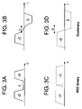
- FIGS. 3A-D graphically illustrate representative distortions in optical binary and duobinary signals due to dispersion effects in an optical link
- FIGS. 4A-B show a representative eye diagram of a (10 Gb/s) duobinary signal and the corresponding noise distribution function, respectively, in the system of FIG. 1 ;
- FIG. 5 shows a block diagram of a receiver that can be used in the system of FIG. 1 according to one embodiment of the present invention.
- FIGS. 6-8 graphically compare performance characteristics of different configurations of the system shown in FIG. 1 .
- FIG. 1 shows a block diagram of a representative optical communication system 100 adapted to use optical duobinary coding.
- System 100 has a duobinary transmitter 102 coupled to a receiver 108 via a transmission link having an optical fiber 104 and one or more optical amplifiers 106 .
- Transmitter 102 receives a binary sequence, a k , and generates a corresponding optical duobinary signal, A(t), which is received as signal S(t) at receiver 108 .
- signal S(t) may have distortions due to chromatic dispersion (CD) and polarization mode dispersion (PMD) in fiber 104 and/or amplification noise in amplifier 106 .
- Receiver 108 converts optical signal S(t) into a corresponding electrical signal and processes that signal to generate binary sequence a′ k . corresponding to sequence a k .
- duobinary transmitters that can be used as transmitter 102 can be found, for example, in the following articles: (1) J. M. Gene et al., IEEE Photonics Technology Letters, 2002, vol. 14, p. 843; (2) W. Kaiser et al., IEEE Photonics Technology Letters, 2001, vol. 13, p. 884; (3) H. Kim and C. X. Yu, IEEE Photonics Technology Letters, 2002, vol. 14, p. 1205; and (4) H. Bissessur, Electronics Letters, 2001, vol. 37, p. 45, the teachings of all of which are incorporated herein by reference.
- FIG. 2 shows a block diagram of a receiver 200 that can be used as receiver 108 in system 100 .
- Receiver 200 has an optical-to-electrical (O/E) signal converter (e.g., a photodiode) 206 that converts optical signal S(t) into electrical signal S′(t) whose amplitude is proportional to the optical power of signal S(t).
- O/E optical-to-electrical
- a decoder 208 samples signal S′(t), e.g., by integrating it over a fraction of each bit length termed a “sampling window,” and compares the integration result with a decision threshold value. Based on the comparison, decoder 208 outputs either digital “1” or digital “0” for sequence a′ k .
- Optimal performance of decoder 208 is achieved when both the width of the sampling window and the decision threshold value are appropriately selected to minimize the number of decoding errors arising from the presence of distortions and noise in signal S′(t).
- FIGS. 3A-D graphically illustrate representative distortions in optical binary and duobinary signals due to dispersion effects in an optical link, e.g., fiber 104 in system 100 .
- the waveforms shown in FIGS. 3A-D represent a simplified graphical depiction of actual waveforms that may be used in system 100 .
- a “101” binary sequence is mapped onto the optical domain as “+E, 0, +E” in optical binary NRZ (non-return-to-zero) coding ( FIG. 3A ) and as “+E, 0, ⁇ E” in optical duobinary coding ( FIG. 3B ).
- One effect of dispersion is to broaden optical pulses as shown in FIGS. 3C-D .
- broadened optical pulses of the NRZ waveform interfere constructively in the area corresponding to the optical “0,” thereby making it difficult to properly decode said “0” at the receiver.
- broadened optical pulses of the duobinary waveform interfere destructively in the area corresponding to the optical “0,” which may preserve a relatively narrow “valley” between two optical “ones” and improve chances of properly decoding said “0” at the receiver.
- FIGS. 4A-B show a representative eye diagram of (10 Gb/s) signal S(t) and the corresponding noise distribution function, respectively, in system 100 .
- the eye diagram shows different waveforms that may be transmitted in system 100 over a time interval corresponding to two bit periods.
- waveform 402 having a relatively broad pulse centered at about 100 ps corresponds to a “010” binary sequence.
- waveform 404 having a relatively narrow valley centered at about 100 ps corresponds to a “101” binary sequence.
- waveforms shown in FIG. 4A correspond to “111”, “110”, “100”, “000”, “001”, and “011” bit sequences. Referring to FIG.
- the total noise is dominated by the spontaneous beat noise in optical amplifiers, e.g., amplifiers 106 ( FIG. 1 ).
- the “space” level i.e., the level corresponding to binary “0”
- the total noise is dominated by thermal noise.
- sampling windows A and B correspond to prior-art configurations of decoder 208 and sampling window D corresponds to a novel configuration of the decoder according to one embodiment of the present invention.
- the sampling window has a relatively large width, e.g., greater than 30% of the bit length.
- One consideration for choosing a relatively large width value is that longer integration times typically reduce decoding errors due to noise averaging. It is generally believed that setting a relatively narrow sampling window will reduce the benefits of noise averaging and detrimentally affect performance of receiver 200 .
- using a relatively wide sampling window increases decoding errors due to wrong interpretation of zeros in “101” binary fragments (see FIGS. 3C-D ).
- analogous decoding errors may be caused by dispersion-free signals utilizing relatively large duty-cycle values, e.g., greater than 1 (see FIG. 4A ). As discussed below, attempts to reduce said errors by simply adjusting the decision threshold value are largely ineffective.
- waveform 404 has a relatively narrow valley between two relatively broad pulses.
- Sampling windows A and B have different decision threshold values but identical widths.
- the integration result corresponding to waveform 404 may have a relatively large contribution from the part of the waveform corresponding to the trailing edge of the preceding optical “1” and the part of the waveform corresponding to the leading edge of the next optical “1”. This increases the probability of decoding errors because, even in the absence of noise, the gap between the decision threshold value and the integration result of waveform 404 is relatively narrow.
- the contribution of noise may then easily cause the integration result to overshoot the decision threshold value, thereby causing a decoding error for waveform 404 .
- raising the decision threshold value to that of sampling window B will narrow the gap between the decision threshold value and the noise-free integration result of waveform 402 .
- the contribution of signal spontaneous beat noise may then cause the integration result to undershoot the decision threshold value, thereby causing a decoding error for waveform 402 . In either case, the number of decoding errors is relatively large.
- the number of decoding errors in decoder 208 can be reduced for duobinary signals by decreasing the sampling window width and properly aligning said window with respect to the waveforms of the signal.
- sampling window D is used for waveform 404 ( FIG. 4A )
- the contribution into the integration result from the part of the waveform corresponding to the trailing edge of the preceding optical “1” and the part of the waveform corresponding to the leading edge of the next optical “1” is significantly reduced compared to the configuration where window A or window B is used. This decreases the probability of decoding errors because the gap between the decision threshold value and the integration result of noise-free waveform 404 can now be relatively large.
- the decision threshold value itself may now be selected to correspond to the “low noise” region without incurring a relatively large penalty from the trailing/leading edges of the adjacent optical “ones.” As a result, the overall contribution of noise into the integration results is reduced. Furthermore, the gap between the decision threshold value and the noise-free integration result of waveform 402 becomes relatively wide. Therefore, it becomes more difficult for the contribution of signal spontaneous beat noise ( FIG. 4B ) to cause said integration result to undershoot the decision threshold value, which further reduces the number of decoding errors.
- the width of sampling window D for decoder 208 is selected based on an eye diagram similar to that shown in FIG. 4A .
- the sampling window width is selected to be even narrower than the “zero” valley, e.g., as illustrated in FIG. 4A .
- the width of sampling window D is less than about 25% of the bit length or preferably fixed at about 10% of the bit length.
- FIG. 5 shows a block diagram of a receiver 500 that can be used as receiver 108 in system 100 according to one embodiment of the present invention. Similar to receiver 200 of FIG. 2 , receiver 500 is adapted to receive optical duobinary signal S(t) and convert it into a corresponding binary sequence a′ k . Receiver 500 has an O/E signal converter 506 that is similar to converter 206 of receiver 200 . A decoder 508 samples signal S′(t) generated by converter 506 , e.g., using a configuration corresponding to sampling window D of FIG. 4A . To provide an appropriate time reference for aligning the sampling window, receiver 500 has a clock recovery circuit 502 and a clock multiplier 504 .
- Circuit 502 processes signal S′(t) to generate a first clock signal synchronized with signal S′(t).
- Clock multiplier 504 multiplies the frequency of the first clock signal and generates a second clock signal applied to decoder 508 .
- the second clock signal has a frequency value four times that of the first clock.
- Decoder 508 uses clock pulses to align sampling window D with respect to signal S′(t).
- the width of the sampling window may be selected based on the inter-pulse separation in the second clock signal.
- synchronization techniques may similarly be used.
- FIGS. 6-8 graphically compare performance characteristics of two different configurations of system 100 . More specifically, FIGS. 6-7 show dispersion tolerance at bit error rate (BER) of 10 ⁇ 3 , and FIG. 8 shows dependence of BER on the power of signal S(t).
- transmitter 102 is a transmitter based on a Mach-Zehnder modulator operating at a bit rate of 10 Gb/s.
- receiver 108 is receiver 500 ( FIG. 5 ), wherein the second clock signal has a frequency value corresponding to four times the bit rate.
- receiver 108 is receiver 200 ( FIG. 2 ), which has (i) a sampling window width corresponding to that of sampling windows A and B shown in FIG. 4 and (ii) a decision threshold value set at about 25% of the mark level.
- configuration I provides optical signal-to-noise (OSNR) gain of about 1 dB with respect to configuration II for chromatic dispersion values between 0 and about 4000 ps/nm.
- OSNR optical signal-to-noise
- configuration I consistently out performs configuration II for PMD-affected signals having differential group delay (DGD) values between 0 and about 50 ps.
- DDD differential group delay
- configuration I improves PMD tolerance by about 20%.
- configuration I provides substantial gain over configuration II in terms of the optical power at the receiver.
- configuration I lowers the coresponding optical power by about 3 dB with respect to that in configuration II.
- embodiments of the present invention improve dispersion tolerance and reduce optical power corresponding to a selected BER value in duobinary transmission systems, thereby improving overall back-to-back (i.e., source-to-destination) performance of such systems.
- the present invention may be implemented as circuit-based processes, including possible implementation on a single integrated circuit.
- various functions of circuit elements may also be implemented as processing steps in a software program.
- Such software may be employed in, for example, a digital signal processor, micro-controller, or general-purpose computer.
Abstract
Description
Claims (19)
Priority Applications (6)
| Application Number | Priority Date | Filing Date | Title |
|---|---|---|---|
| US10/730,413 US7613402B2 (en) | 2003-12-08 | 2003-12-08 | Duobinary receiver |
| EP04257203A EP1542417B1 (en) | 2003-12-08 | 2004-11-22 | Duobinary receiver |
| DE602004006946T DE602004006946T2 (en) | 2003-12-08 | 2004-11-22 | Duobinary receiver |
| KR1020040101226A KR101138630B1 (en) | 2003-12-08 | 2004-12-03 | Duobinary receiver |
| CN2004101002123A CN1627667B (en) | 2003-12-08 | 2004-12-07 | Duobinary receiver |
| JP2004354755A JP4629423B2 (en) | 2003-12-08 | 2004-12-08 | Duobinary receiver |
Applications Claiming Priority (1)
| Application Number | Priority Date | Filing Date | Title |
|---|---|---|---|
| US10/730,413 US7613402B2 (en) | 2003-12-08 | 2003-12-08 | Duobinary receiver |
Publications (2)
| Publication Number | Publication Date |
|---|---|
| US20050123068A1 US20050123068A1 (en) | 2005-06-09 |
| US7613402B2 true US7613402B2 (en) | 2009-11-03 |
Family
ID=34523010
Family Applications (1)
| Application Number | Title | Priority Date | Filing Date |
|---|---|---|---|
| US10/730,413 Expired - Fee Related US7613402B2 (en) | 2003-12-08 | 2003-12-08 | Duobinary receiver |
Country Status (6)
| Country | Link |
|---|---|
| US (1) | US7613402B2 (en) |
| EP (1) | EP1542417B1 (en) |
| JP (1) | JP4629423B2 (en) |
| KR (1) | KR101138630B1 (en) |
| CN (1) | CN1627667B (en) |
| DE (1) | DE602004006946T2 (en) |
Cited By (2)
| Publication number | Priority date | Publication date | Assignee | Title |
|---|---|---|---|---|
| US20030170022A1 (en) * | 2002-03-06 | 2003-09-11 | Lucent Technologies Inc. | Method and apparatus for improved jitter tolerance |
| WO2019160838A1 (en) | 2018-02-14 | 2019-08-22 | Nokia Solutions And Networks Oy | Multi-rate optical network |
Families Citing this family (6)
| Publication number | Priority date | Publication date | Assignee | Title |
|---|---|---|---|---|
| DE10319561B4 (en) * | 2003-04-30 | 2005-05-04 | Siemens Ag | Method for operating a digital interface arrangement and digital interface arrangement for exchanging data |
| US7447278B2 (en) * | 2003-05-21 | 2008-11-04 | International Business Machines Corporation | Apparatus for transmitting and receiving data |
| JP4888393B2 (en) * | 2005-09-28 | 2012-02-29 | 日本電気株式会社 | Clock regeneration apparatus and method |
| US9025702B2 (en) * | 2011-08-26 | 2015-05-05 | Fujitsu Limited | Method and apparatus for implementing slice-level adjustment |
| US20130272721A1 (en) * | 2012-04-13 | 2013-10-17 | Alcatel-Lucent Usa, Inc. | Optical network device employing three-level duobinary modulation and method of use thereof |
| US8929428B2 (en) * | 2012-10-30 | 2015-01-06 | International Business Machines Corporation | Feed-forward equalization in a receiver |
Citations (23)
| Publication number | Priority date | Publication date | Assignee | Title |
|---|---|---|---|---|
| US4144565A (en) | 1977-01-06 | 1979-03-13 | International Business Machines Corporation | Input/output interface connector circuit for repowering and isolation |
| WO1985005234A1 (en) | 1984-05-07 | 1985-11-21 | D.A.V.I.D. Systems, Inc. | High-speed digital loop transceiver |
| US4780888A (en) * | 1985-09-19 | 1988-10-25 | Tandberg Data A/S | Method and arrangement for disturbance-proof recognition of data contained in data signals |
| EP0508885A2 (en) | 1991-04-08 | 1992-10-14 | Digital Equipment Corporation | A synchronous decoder for self-clocking signals |
| US5351271A (en) | 1991-12-19 | 1994-09-27 | Institut Francais Du Petrole | Method and device for measuring the successive amplitude levels of signals received on a transmission channel |
| US5453826A (en) * | 1992-09-29 | 1995-09-26 | Anritsu Corporation | Optical time domain reflectometer employing synchronizing signals to synchronize the sampling and manipulation of data representing fibers optic characteristics |
| US5774064A (en) | 1987-05-21 | 1998-06-30 | Trw Inc. | Remote control system for door locks |
| US5777765A (en) * | 1995-09-20 | 1998-07-07 | Alcatel N.V. | Optical delay unit, optical line emulator including such a unit and methods realized by such an optical delay unit and by such an optical line emulator |
| US5867534A (en) | 1994-04-20 | 1999-02-02 | Alcatel Cit | Optical transmission method with reduced sensitivity to dispersion, transmission device and system for implementing this method |
| DE19823705A1 (en) | 1998-05-27 | 1999-12-02 | Siemens Ag | Method and circuit arrangement for restoring a binary signal |
| US6188497B1 (en) | 1997-02-13 | 2001-02-13 | Lucent Technologies Inc. | Duo-binary signal encoding |
| US6295152B1 (en) | 1997-12-11 | 2001-09-25 | Alcatel | Optical receiver for receiving digitally transmitted data |
| US20030002833A1 (en) | 2001-06-29 | 2003-01-02 | Fujitsu Limited | Method and device for measuring the waveform of an optical signal |
| US20030170022A1 (en) * | 2002-03-06 | 2003-09-11 | Lucent Technologies Inc. | Method and apparatus for improved jitter tolerance |
| US20040071247A1 (en) | 2000-12-19 | 2004-04-15 | Dunning David S. | Method and apparatus for a tracking data receiver compensating for deterministic jitter |
| US20040091273A1 (en) * | 2001-12-26 | 2004-05-13 | Patrice Brissette | Receiver monitoring and optimization using forward error correction information |
| US20040151511A1 (en) * | 2003-01-31 | 2004-08-05 | Gill Douglas M. | Apparatus and method for duobinary transmission |
| US6778589B1 (en) | 1998-10-09 | 2004-08-17 | Futaba Denshi Kogyo Kabushiki Kaisha | Symbol synchronous device and frequency hopping receiver |
| US6839130B2 (en) * | 2001-08-03 | 2005-01-04 | Ando Electric Co., Ltd. | Optical fiber measuring apparatus |
| US20050185969A1 (en) | 2004-02-19 | 2005-08-25 | Moeller Lothar Benedict E.J. | Method and apparatus for processing optical duobinary signals |
| US20050232644A1 (en) | 2004-04-20 | 2005-10-20 | Moeller Lothar Benedict E J | Optical heterodyne receiver based on oversampling |
| US7142621B2 (en) | 2001-10-26 | 2006-11-28 | International Business Machines Corporation | Method and circuit for recovering a data signal from a stream of binary data |
| US7173993B2 (en) | 2002-01-30 | 2007-02-06 | Infineon Technologies Ag | Method for sampling phase control |
Family Cites Families (3)
| Publication number | Priority date | Publication date | Assignee | Title |
|---|---|---|---|---|
| US3351271A (en) * | 1965-11-02 | 1967-11-07 | Worthington Corp | Unloading device for reciprocating compressors |
| SE522272C2 (en) * | 1997-08-20 | 2004-01-27 | Ericsson Telefon Ab L M | Optical duobinar transmitter system and method using optical intensity modulation |
| US6295125B1 (en) * | 1999-07-23 | 2001-09-25 | Showa Denko K.K. | Differential refractive index detector and liquid chromatograph equipped with the same |
-
2003
- 2003-12-08 US US10/730,413 patent/US7613402B2/en not_active Expired - Fee Related
-
2004
- 2004-11-22 EP EP04257203A patent/EP1542417B1/en not_active Expired - Fee Related
- 2004-11-22 DE DE602004006946T patent/DE602004006946T2/en active Active
- 2004-12-03 KR KR1020040101226A patent/KR101138630B1/en not_active IP Right Cessation
- 2004-12-07 CN CN2004101002123A patent/CN1627667B/en not_active Expired - Fee Related
- 2004-12-08 JP JP2004354755A patent/JP4629423B2/en not_active Expired - Fee Related
Patent Citations (23)
| Publication number | Priority date | Publication date | Assignee | Title |
|---|---|---|---|---|
| US4144565A (en) | 1977-01-06 | 1979-03-13 | International Business Machines Corporation | Input/output interface connector circuit for repowering and isolation |
| WO1985005234A1 (en) | 1984-05-07 | 1985-11-21 | D.A.V.I.D. Systems, Inc. | High-speed digital loop transceiver |
| US4780888A (en) * | 1985-09-19 | 1988-10-25 | Tandberg Data A/S | Method and arrangement for disturbance-proof recognition of data contained in data signals |
| US5774064A (en) | 1987-05-21 | 1998-06-30 | Trw Inc. | Remote control system for door locks |
| EP0508885A2 (en) | 1991-04-08 | 1992-10-14 | Digital Equipment Corporation | A synchronous decoder for self-clocking signals |
| US5351271A (en) | 1991-12-19 | 1994-09-27 | Institut Francais Du Petrole | Method and device for measuring the successive amplitude levels of signals received on a transmission channel |
| US5453826A (en) * | 1992-09-29 | 1995-09-26 | Anritsu Corporation | Optical time domain reflectometer employing synchronizing signals to synchronize the sampling and manipulation of data representing fibers optic characteristics |
| US5867534A (en) | 1994-04-20 | 1999-02-02 | Alcatel Cit | Optical transmission method with reduced sensitivity to dispersion, transmission device and system for implementing this method |
| US5777765A (en) * | 1995-09-20 | 1998-07-07 | Alcatel N.V. | Optical delay unit, optical line emulator including such a unit and methods realized by such an optical delay unit and by such an optical line emulator |
| US6188497B1 (en) | 1997-02-13 | 2001-02-13 | Lucent Technologies Inc. | Duo-binary signal encoding |
| US6295152B1 (en) | 1997-12-11 | 2001-09-25 | Alcatel | Optical receiver for receiving digitally transmitted data |
| DE19823705A1 (en) | 1998-05-27 | 1999-12-02 | Siemens Ag | Method and circuit arrangement for restoring a binary signal |
| US6778589B1 (en) | 1998-10-09 | 2004-08-17 | Futaba Denshi Kogyo Kabushiki Kaisha | Symbol synchronous device and frequency hopping receiver |
| US20040071247A1 (en) | 2000-12-19 | 2004-04-15 | Dunning David S. | Method and apparatus for a tracking data receiver compensating for deterministic jitter |
| US20030002833A1 (en) | 2001-06-29 | 2003-01-02 | Fujitsu Limited | Method and device for measuring the waveform of an optical signal |
| US6839130B2 (en) * | 2001-08-03 | 2005-01-04 | Ando Electric Co., Ltd. | Optical fiber measuring apparatus |
| US7142621B2 (en) | 2001-10-26 | 2006-11-28 | International Business Machines Corporation | Method and circuit for recovering a data signal from a stream of binary data |
| US20040091273A1 (en) * | 2001-12-26 | 2004-05-13 | Patrice Brissette | Receiver monitoring and optimization using forward error correction information |
| US7173993B2 (en) | 2002-01-30 | 2007-02-06 | Infineon Technologies Ag | Method for sampling phase control |
| US20030170022A1 (en) * | 2002-03-06 | 2003-09-11 | Lucent Technologies Inc. | Method and apparatus for improved jitter tolerance |
| US20040151511A1 (en) * | 2003-01-31 | 2004-08-05 | Gill Douglas M. | Apparatus and method for duobinary transmission |
| US20050185969A1 (en) | 2004-02-19 | 2005-08-25 | Moeller Lothar Benedict E.J. | Method and apparatus for processing optical duobinary signals |
| US20050232644A1 (en) | 2004-04-20 | 2005-10-20 | Moeller Lothar Benedict E J | Optical heterodyne receiver based on oversampling |
Non-Patent Citations (7)
| Title |
|---|
| "Dispersion-Tolerant Optical Transmission System Using Duobinary Transmitter and Binary Receiver," by Kazushige Ynenaga et al., Journal of Lightwave Technology, IEEE. New York, US, ISSN: 0733-8724, vol. 15, No. 18, Aug. 1997, pp. 1530-1537. |
| "Enhanced Phase-Shaped Binary Transmission for Dense WDM Systems," H. Bissessur, et al., Electronics Letters, vol. 37, No. 1, Jan. 2001, pp. 45-46. |
| "Modulating Pulses in Long-Haul Optics Systems" by Anjali Singh, CommDesign Feb. 7, 2002, www.comdesign.com/article/printablearticle.jhtml?articleID=16504367, 9 pages. |
| "Optical Duobinary Transmission System Featuring Improved Receiver Sensitivity and Reduced Optical Bandwidth," by Hoon Kim and Charles X. Yu, IEEE Photonics Technology Letters, vol. 14, No. 8, Aug. 2002. |
| "Reduced Complexity Optical Duobinary 10-Gb/s Transmitter Setup Resulting in an Increased Transmission Distance," by W. Kaiser, et al., IEEE Photonics Technology Letters, vol. 13, No. 8, Aug. 2001, pp. 884-886. |
| "Reduced Driving Voltage Optical Duobinary Transmitter and Its Impact on Transmission Performance Over Standard Single-Mode Fiber," by J.M. Gené, et al., IEEE Photonics Technology Letters, vol. 14, No. 6, Jun. 2002, pp. 843-845. |
| "return to zero binary code", by Martin H. Weik, Fiber Optics Standard Dictionary, 3rd ed., 1997, 3 pages. |
Cited By (3)
| Publication number | Priority date | Publication date | Assignee | Title |
|---|---|---|---|---|
| US20030170022A1 (en) * | 2002-03-06 | 2003-09-11 | Lucent Technologies Inc. | Method and apparatus for improved jitter tolerance |
| US8639127B2 (en) * | 2002-03-06 | 2014-01-28 | Alcatel Lucent | Method and apparatus for improved jitter tolerance |
| WO2019160838A1 (en) | 2018-02-14 | 2019-08-22 | Nokia Solutions And Networks Oy | Multi-rate optical network |
Also Published As
| Publication number | Publication date |
|---|---|
| CN1627667B (en) | 2010-05-05 |
| JP4629423B2 (en) | 2011-02-09 |
| DE602004006946D1 (en) | 2007-07-26 |
| DE602004006946T2 (en) | 2008-02-14 |
| US20050123068A1 (en) | 2005-06-09 |
| CN1627667A (en) | 2005-06-15 |
| KR20050055588A (en) | 2005-06-13 |
| JP2005176374A (en) | 2005-06-30 |
| KR101138630B1 (en) | 2012-04-26 |
| EP1542417B1 (en) | 2007-06-13 |
| EP1542417A1 (en) | 2005-06-15 |
Similar Documents
| Publication | Publication Date | Title |
|---|---|---|
| EP1566904B1 (en) | Method and apparatus for processing optical duobinary signals | |
| US6690894B2 (en) | Multilevel optical signals optimized for systems having signal-dependent and signal-independent noises, finite transmitter extinction ratio and intersymbol interference | |
| US7286762B2 (en) | Apparatus with spread-pulse modulation and nonlinear time domain equalization for fiber optic communication channels | |
| Walklin et al. | Multilevel signaling for increasing the reach of 10 Gb/s lightwave systems | |
| US9306780B2 (en) | Optical transmission for binary and duobinary modulation formats | |
| US6623188B1 (en) | Dispersion tolerant optical data transmitter | |
| US8229303B1 (en) | Reducing pulse narrowing in the transmitter signal that drives a limiting E/O converter for optical fiber channels | |
| US7203429B2 (en) | Optical transmission system using optical signal processing in terminals for improved system performance | |
| US7613402B2 (en) | Duobinary receiver | |
| Sun et al. | Towards low carrier-to-signal power ratio for Kramers-Kronig receiver | |
| Bendimerad et al. | Nonlinearity-tolerant 8D modulation formats by set-partitioning PDM-QPSK | |
| US6404819B1 (en) | System and method for generating NRZ signals from RZ signals in communications networks | |
| US20050024253A1 (en) | Duobinary-to-binary signal converter | |
| EP1318639B1 (en) | Digital transmission system with receiver using parallel decision circuits | |
| US6917233B1 (en) | Limiting amplifier and method for amplifying an input signal | |
| WO2022100860A1 (en) | Detecting intensity modulated optical signal by low bandwidth receiving device | |
| WO2006043268A1 (en) | A system and method for increasing transmission distance of an optical signal | |
| US20220182150A1 (en) | Encoding and Decoding Communications Traffic in a Pulse Amplitude Modulation Format and Optical Apparatus for Same | |
| WO2003067790A1 (en) | Dispersion tolerant optical data transmitter |
Legal Events
| Date | Code | Title | Description |
|---|---|---|---|
| AS | Assignment |
Owner name: LUCENT TECHNOLOGIES INC., NEW JERSEY Free format text: ASSIGNMENT OF ASSIGNORS INTEREST;ASSIGNORS:LIU, XIANG;MOELLER, LOTHAR BENEDICT ERHARD JOSEF;WEI, XING;AND OTHERS;REEL/FRAME:014777/0007;SIGNING DATES FROM 20031125 TO 20031202 |
|
| FEPP | Fee payment procedure |
Free format text: PAYOR NUMBER ASSIGNED (ORIGINAL EVENT CODE: ASPN); ENTITY STATUS OF PATENT OWNER: LARGE ENTITY |
|
| AS | Assignment |
Owner name: ALCATEL-LUCENT USA INC., NEW JERSEY Free format text: MERGER;ASSIGNOR:LUCENT TECHNOLOGIES INC.;REEL/FRAME:023232/0900 Effective date: 20081101 |
|
| STCF | Information on status: patent grant |
Free format text: PATENTED CASE |
|
| CC | Certificate of correction | ||
| AS | Assignment |
Owner name: CREDIT SUISSE AG, NEW YORK Free format text: SECURITY INTEREST;ASSIGNOR:ALCATEL-LUCENT USA INC.;REEL/FRAME:030510/0627 Effective date: 20130130 |
|
| FPAY | Fee payment |
Year of fee payment: 4 |
|
| AS | Assignment |
Owner name: ALCATEL LUCENT, FRANCE Free format text: ASSIGNMENT OF ASSIGNORS INTEREST;ASSIGNOR:ALCATEL-LUCENT USA INC.;REEL/FRAME:030410/0341 Effective date: 20130514 |
|
| AS | Assignment |
Owner name: ALCATEL-LUCENT USA INC., NEW JERSEY Free format text: RELEASE BY SECURED PARTY;ASSIGNOR:CREDIT SUISSE AG;REEL/FRAME:033950/0261 Effective date: 20140819 |
|
| FPAY | Fee payment |
Year of fee payment: 8 |
|
| AS | Assignment |
Owner name: PROVENANCE ASSET GROUP LLC, CONNECTICUT Free format text: ASSIGNMENT OF ASSIGNORS INTEREST;ASSIGNORS:NOKIA TECHNOLOGIES OY;NOKIA SOLUTIONS AND NETWORKS BV;ALCATEL LUCENT SAS;REEL/FRAME:043877/0001 Effective date: 20170912 Owner name: NOKIA USA INC., CALIFORNIA Free format text: SECURITY INTEREST;ASSIGNORS:PROVENANCE ASSET GROUP HOLDINGS, LLC;PROVENANCE ASSET GROUP LLC;REEL/FRAME:043879/0001 Effective date: 20170913 Owner name: CORTLAND CAPITAL MARKET SERVICES, LLC, ILLINOIS Free format text: SECURITY INTEREST;ASSIGNORS:PROVENANCE ASSET GROUP HOLDINGS, LLC;PROVENANCE ASSET GROUP, LLC;REEL/FRAME:043967/0001 Effective date: 20170913 |
|
| AS | Assignment |
Owner name: NOKIA US HOLDINGS INC., NEW JERSEY Free format text: ASSIGNMENT AND ASSUMPTION AGREEMENT;ASSIGNOR:NOKIA USA INC.;REEL/FRAME:048370/0682 Effective date: 20181220 |
|
| FEPP | Fee payment procedure |
Free format text: MAINTENANCE FEE REMINDER MAILED (ORIGINAL EVENT CODE: REM.); ENTITY STATUS OF PATENT OWNER: LARGE ENTITY |
|
| AS | Assignment |
Owner name: PROVENANCE ASSET GROUP LLC, CONNECTICUT Free format text: RELEASE BY SECURED PARTY;ASSIGNOR:CORTLAND CAPITAL MARKETS SERVICES LLC;REEL/FRAME:058983/0104 Effective date: 20211101 Owner name: PROVENANCE ASSET GROUP HOLDINGS LLC, CONNECTICUT Free format text: RELEASE BY SECURED PARTY;ASSIGNOR:CORTLAND CAPITAL MARKETS SERVICES LLC;REEL/FRAME:058983/0104 Effective date: 20211101 Owner name: PROVENANCE ASSET GROUP LLC, CONNECTICUT Free format text: RELEASE BY SECURED PARTY;ASSIGNOR:NOKIA US HOLDINGS INC.;REEL/FRAME:058363/0723 Effective date: 20211129 Owner name: PROVENANCE ASSET GROUP HOLDINGS LLC, CONNECTICUT Free format text: RELEASE BY SECURED PARTY;ASSIGNOR:NOKIA US HOLDINGS INC.;REEL/FRAME:058363/0723 Effective date: 20211129 |
|
| LAPS | Lapse for failure to pay maintenance fees |
Free format text: PATENT EXPIRED FOR FAILURE TO PAY MAINTENANCE FEES (ORIGINAL EVENT CODE: EXP.); ENTITY STATUS OF PATENT OWNER: LARGE ENTITY |
|
| STCH | Information on status: patent discontinuation |
Free format text: PATENT EXPIRED DUE TO NONPAYMENT OF MAINTENANCE FEES UNDER 37 CFR 1.362 |
|
| AS | Assignment |
Owner name: RPX CORPORATION, CALIFORNIA Free format text: ASSIGNMENT OF ASSIGNORS INTEREST;ASSIGNOR:PROVENANCE ASSET GROUP LLC;REEL/FRAME:059352/0001 Effective date: 20211129 |
|
| FP | Lapsed due to failure to pay maintenance fee |
Effective date: 20211103 |