US7615477B2 - Method of fabricating a BGA package having decreased adhesion - Google Patents
Method of fabricating a BGA package having decreased adhesion Download PDFInfo
- Publication number
- US7615477B2 US7615477B2 US11/566,956 US56695606A US7615477B2 US 7615477 B2 US7615477 B2 US 7615477B2 US 56695606 A US56695606 A US 56695606A US 7615477 B2 US7615477 B2 US 7615477B2
- Authority
- US
- United States
- Prior art keywords
- pad
- bga
- fabricating
- laminate
- conductive foil
- Prior art date
- Legal status (The legal status is an assumption and is not a legal conclusion. Google has not performed a legal analysis and makes no representation as to the accuracy of the status listed.)
- Expired - Fee Related, expires
Links
Images


Classifications
-
- H—ELECTRICITY
- H05—ELECTRIC TECHNIQUES NOT OTHERWISE PROVIDED FOR
- H05K—PRINTED CIRCUITS; CASINGS OR CONSTRUCTIONAL DETAILS OF ELECTRIC APPARATUS; MANUFACTURE OF ASSEMBLAGES OF ELECTRICAL COMPONENTS
- H05K1/00—Printed circuits
- H05K1/02—Details
- H05K1/0271—Arrangements for reducing stress or warp in rigid printed circuit boards, e.g. caused by loads, vibrations or differences in thermal expansion
-
- H—ELECTRICITY
- H01—ELECTRIC ELEMENTS
- H01L—SEMICONDUCTOR DEVICES NOT COVERED BY CLASS H10
- H01L23/00—Details of semiconductor or other solid state devices
- H01L23/48—Arrangements for conducting electric current to or from the solid state body in operation, e.g. leads, terminal arrangements ; Selection of materials therefor
- H01L23/488—Arrangements for conducting electric current to or from the solid state body in operation, e.g. leads, terminal arrangements ; Selection of materials therefor consisting of soldered or bonded constructions
- H01L23/498—Leads, i.e. metallisations or lead-frames on insulating substrates, e.g. chip carriers
- H01L23/49866—Leads, i.e. metallisations or lead-frames on insulating substrates, e.g. chip carriers characterised by the materials
-
- H—ELECTRICITY
- H05—ELECTRIC TECHNIQUES NOT OTHERWISE PROVIDED FOR
- H05K—PRINTED CIRCUITS; CASINGS OR CONSTRUCTIONAL DETAILS OF ELECTRIC APPARATUS; MANUFACTURE OF ASSEMBLAGES OF ELECTRICAL COMPONENTS
- H05K3/00—Apparatus or processes for manufacturing printed circuits
- H05K3/40—Forming printed elements for providing electric connections to or between printed circuits
- H05K3/4092—Integral conductive tabs, i.e. conductive parts partly detached from the substrate
-
- H—ELECTRICITY
- H01—ELECTRIC ELEMENTS
- H01L—SEMICONDUCTOR DEVICES NOT COVERED BY CLASS H10
- H01L2924/00—Indexing scheme for arrangements or methods for connecting or disconnecting semiconductor or solid-state bodies as covered by H01L24/00
- H01L2924/0001—Technical content checked by a classifier
- H01L2924/0002—Not covered by any one of groups H01L24/00, H01L24/00 and H01L2224/00
-
- H—ELECTRICITY
- H05—ELECTRIC TECHNIQUES NOT OTHERWISE PROVIDED FOR
- H05K—PRINTED CIRCUITS; CASINGS OR CONSTRUCTIONAL DETAILS OF ELECTRIC APPARATUS; MANUFACTURE OF ASSEMBLAGES OF ELECTRICAL COMPONENTS
- H05K1/00—Printed circuits
- H05K1/02—Details
- H05K1/11—Printed elements for providing electric connections to or between printed circuits
- H05K1/111—Pads for surface mounting, e.g. lay-out
-
- H—ELECTRICITY
- H05—ELECTRIC TECHNIQUES NOT OTHERWISE PROVIDED FOR
- H05K—PRINTED CIRCUITS; CASINGS OR CONSTRUCTIONAL DETAILS OF ELECTRIC APPARATUS; MANUFACTURE OF ASSEMBLAGES OF ELECTRICAL COMPONENTS
- H05K2201/00—Indexing scheme relating to printed circuits covered by H05K1/00
- H05K2201/01—Dielectrics
- H05K2201/0104—Properties and characteristics in general
- H05K2201/0133—Elastomeric or compliant polymer
-
- H—ELECTRICITY
- H05—ELECTRIC TECHNIQUES NOT OTHERWISE PROVIDED FOR
- H05K—PRINTED CIRCUITS; CASINGS OR CONSTRUCTIONAL DETAILS OF ELECTRIC APPARATUS; MANUFACTURE OF ASSEMBLAGES OF ELECTRICAL COMPONENTS
- H05K2201/00—Indexing scheme relating to printed circuits covered by H05K1/00
- H05K2201/03—Conductive materials
- H05K2201/0332—Structure of the conductor
- H05K2201/0335—Layered conductors or foils
- H05K2201/0355—Metal foils
-
- H—ELECTRICITY
- H05—ELECTRIC TECHNIQUES NOT OTHERWISE PROVIDED FOR
- H05K—PRINTED CIRCUITS; CASINGS OR CONSTRUCTIONAL DETAILS OF ELECTRIC APPARATUS; MANUFACTURE OF ASSEMBLAGES OF ELECTRICAL COMPONENTS
- H05K2203/00—Indexing scheme relating to apparatus or processes for manufacturing printed circuits covered by H05K3/00
- H05K2203/03—Metal processing
- H05K2203/0307—Providing micro- or nanometer scale roughness on a metal surface, e.g. by plating of nodules or dendrites
-
- H—ELECTRICITY
- H05—ELECTRIC TECHNIQUES NOT OTHERWISE PROVIDED FOR
- H05K—PRINTED CIRCUITS; CASINGS OR CONSTRUCTIONAL DETAILS OF ELECTRIC APPARATUS; MANUFACTURE OF ASSEMBLAGES OF ELECTRICAL COMPONENTS
- H05K2203/00—Indexing scheme relating to apparatus or processes for manufacturing printed circuits covered by H05K3/00
- H05K2203/11—Treatments characterised by their effect, e.g. heating, cooling, roughening
- H05K2203/1152—Replicating the surface structure of a sacrificial layer, e.g. for roughening
-
- H—ELECTRICITY
- H05—ELECTRIC TECHNIQUES NOT OTHERWISE PROVIDED FOR
- H05K—PRINTED CIRCUITS; CASINGS OR CONSTRUCTIONAL DETAILS OF ELECTRIC APPARATUS; MANUFACTURE OF ASSEMBLAGES OF ELECTRICAL COMPONENTS
- H05K3/00—Apparatus or processes for manufacturing printed circuits
- H05K3/38—Improvement of the adhesion between the insulating substrate and the metal
- H05K3/382—Improvement of the adhesion between the insulating substrate and the metal by special treatment of the metal
- H05K3/384—Improvement of the adhesion between the insulating substrate and the metal by special treatment of the metal by plating
Definitions
- the present invention relates to a wired board (i.e., a board provided with interconnecting conductors or wiring) for use as a BGA (ball grid array) package base for IC (integrated circuit) packages.
- a wired board i.e., a board provided with interconnecting conductors or wiring
- BGA ball grid array
- IC integrated circuit
- the QFP type makes it difficult to cope with a multi-pin arrangement because it is so configured that leads to be connected to a packaging substrate are concentrated only at a peripheral portion of the package when they are also liable to be deformed due to the small diameter thereof.
- the PGA type has a limitation in that it presents difficulties in coping with both high speed processing and surface packaging because it is so configured that the terminals to be connected to a packaging substrate are elongated and very collectively arranged.
- a ball grid array (BGA) package has been disclosed in U.S. Pat. No. 5,148,265, which has ball-like connection terminals over the entire packaging surface of a carrier substrate electrically connected to a semiconductor chip by gold wire bonding.
- the terminals to be connected to the packaging substrate are formed into ball-like shapes and are arrayed over substantially the entire packaging surface without deforming the leads as the case for the QFP. Therefore the pitch between the terminals become larger, thereby making surface packaging easier.
- the connection terminals are shorter than in a QFP package, the inductance component becomes smaller and thereby the signal transmission speed becomes greater. The resulting BGA package is therefore amenable to high speed processing.
- a conventional BGA package base includes a substrate made of an electrically insulating material such as alumina ceramic and a number of connection terminals or bumps formed on the main surface of the substrate.
- Each connection terminal includes a solder ball bonded to a bonding pad by way of a mass of solder.
- the bonding pad is formed on a main surface of a substrate treated by a predetermined plating process.
- the mass of solder typically consists of Pb—Sn eutectic solder or a similar, low melting point solder.
- the solder ball itself, is made of a relatively high melting point solder, typically containing a high percentage of lead (Pb), as for example Pb90-Sn10.
- connection terminal is bonded to the plated surface of the bonding pad by means of the solder mass, thereby constituting a connection terminal.
- the wired board is mounted on a printed board having bonding pads corresponding in arrangement to those of the wired board in such a manner that their connection terminals are respectively aligned with each other, and then the respective terminals are bonded, electrically connecting the wire board to the printed board.
- FIG. 1 illustrates a conventional fabrication technique.
- Substrate 100 is shown with a copper foil having a smooth surface 103 and a rough, dendritic surface 105 bonded to a dielectric 107 .
- dielectric 107 can be the dielectric of a single or multilayer substrate.
- the surface of dielectric 107 is imparted with a rough texture through lamination with the dendritic side of the external copper foil.
- FIG. 2 conventional subtractive circuitization is illustrated.
- a negative acting photoresist 209 is applied to the upper surface of copper foil 203 . After development, openings 211 are formed in the resist.
- FIG. 3 illustrates the prior art BGA pad after etching and stripping of the resist.
- BGA pad 309 is shown anchored to dielectric 307 by the dendritic copper surface 305 . It is understood that substantially the entire surface topography of dielectric substrate 300 is dominated by a “replica” of the dendritic surface.
- the dendritic topography provides enhanced adhesion.
- the BGA pads remain ‘anchored’ to the laminate surface through this dendritic structure. As the laminate surface expands and contracts with the thermal excursions the BGA pad moves with the surface. This can place excessive stress on the package.
- the solder ball anchors the pad to the chip. As the BGA pad moves with the laminate, the stress can fracture the solder connection causing failure. Accordingly, it would be desirable to provide enhanced BGA life.
- the present invention achieves this goal by reducing the adhesion of the BGA pad to the laminate.
- the present invention relates to a method of fabricating a BGA package having decreased adhesion of the BGA pad to the laminate surface.
- the present invention further relates to the BGA package fabricated using the inventive method.
- One aspect of the present invention is concerned with a method which comprises applying dendritic foil to the laminate surface of the package, selectively masking the dendritic foil leaving the BGA target area unmasked, and subsequently smoothing the exposed surface of the dendritic foil.
- an electrically-conductive, “springboard” means is interposed between the BGA pad and the laminate surface.
- the springboard facilitates electrical conduction while permitting the BGA pad to move independently of the laminate surface in response to thermal cycling.
- the springboard means comprise: a semiconductor substrate; a first compliant dielectric layer formed over said substrate and having at least one first opening formed therein; a first BGA pad formed in said first opening and in electrical contact with said substrate; a second compliant dielectric layer formed over said first compliant layer and having at least one second opening formed therein wherein said second opening is substantially offset from said first opening; a second BGA pad formed in said second opening and in electrical contact with said first BGA pad; a soldermask layer formed over said second compliant layer and having a third opening therethrough in communication with said second BGA pad; a solder ball solderably connected to said second BGA pad and extending through said third opening.
- FIGS. 1-3 illustrate fabrication of a prior art BGA pad
- FIGS. 4-6 illustrate fabrication of a first embodiment of the inventive BGA pad
- FIGS. 7-11 illustrate fabrication of a second embodiment of the inventive BGA pad
- FIG. 12 illustrates fabrication of a third embodiment of the inventive BGA pad
- FIGS. 13-19 illustrate fabrication of a fourth embodiment of the inventive BGA pad.
- the laminate surface is imparted with a ‘rough’ surface through lamination with an external copper foil.
- Increased adhesion is provided by the dendritic structure 105 of the copper foil penetrating into the laminate.
- the dendritic side of the copper foil is the primary means of adhesion. This adhesion is further promoted by individual suppliers proprietary means of creating the dendritic structure or by chemical treatments that a supplier may apply to the dendritic “treated” side of the foil.
- the replicate structure imparted by the rough side of the foil is still present and will afford enhanced adhesion of soldermasks, photoresists, etc in downstream processes.
- additional processing such as precious metal plating, soldermasks, etc., follow the circuitization, with the resultant structure having a solder ball on the BGA pad.
- the dendritic topography remains affording enhanced adhesion.
- the BGA pads 309 remain ‘anchored’ to the laminate surface through this dendritic structure.
- the BGA pad is also constrained in place by the aforementioned solder ball that in the final structure is connected to the main PWB package assembly. As the laminate surface expands and contracts with the thermal excursions the BGA pad 309 moves with the surface. This can place excessive stress on the package which results in either a fracture in the solder ball or fracture of the respective circuit traces associated the BGA pad on the carrier or the assembled PWB.
- the present invention comprises a BGA package having decreased adhesion of the BGA pad to the laminate surface.
- the upper surface 401 of dielectric substrate 400 is laminated with external copper foil 407 but in contrast with the prior art, the present invention contacts the less adhesive, shiny side 409 of the foil with the laminate surface 405 .
- a negative acting photoresist 509 is applied to the upper surface (in this embodiment, the dendritic surface) of copper foil 503 . After development, openings 511 are formed in the resist 509 .
- FIG. 6 illustrating the inventive BGA pad after etching and stripping of the resist 509 .
- BGA pad 613 is shown laminated to dielectric 605 by the smooth copper surface 609 .
- the smooth topography provides decreased adhesion relative to that provided by the dendritic surface of the prior art BGA pad.
- the inventive BGA pad 613 has an enhanced ability to move relative to the surface of dielectric 605 .
- the stress applied to the solder balls is decreased reducing the tendency to fracture the solder connections and thereby reducing the occurrence of failures.
- FIG. 7 fabrication of a second embodiment of the present invention as an pattern plated structure plate is illustrated.
- Copper foil 705 is laminated to dielectric substrate 707 in the conventional manner such that the dendritic side 703 of the copper foil contacts and imparts a roughened topology to the top surface of dielectric 707 .
- the smooth side of the copper is located as the top surface 701 .
- the surface copper is etched off, exposing the dielectric surface 804 now having a dendritic topology as illustrated in FIG. 8 .
- the dielectric surface topology is smoothed by any of the techniques known in the art such as plasma, vapor, or other chemical or mechanical attack. These techniques are standard to the art and need not be discussed herein in any detail. Substantially the entire dielectric surface 906 may be smoothed or optionally, the surface may be masked and only selected portion where the BGA pad will be subsequently sited may be treated. Following smoothing, a first metallization layer, comprising a catalyst seed layer 910 is applied. Metallization of dielectric substrates, such as by such as by the deposition of a palladium, palladium/tin or other similar catalysts to initiate metal plating is known to the art. Further, to one skilled in the art of metal depositions, the catalyzing layer could be thin sputter or electrodeposited metal layer.
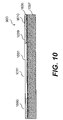
- FIG. 10 A layer of photoresist 1009 , patterned with openings 1011 , is applied to the smoothed dielectric surface 1006 .
- the inventive BGA pad 1109 is shown after a second metallization and photo resist strip steps.
- the second metallization step to form the BGA pad 1109 is preferably copper, but could be nickel, gold, palladium.
- the second metallization can be by electroless or electrolytic means, methods of which are known to the art and do not need explanation here. These methods may utilize multiple plating steps to achieve the required pad height.
- the catalyst layer 910 may be removed.
- This embodiment shows the inventive feature of the present invention wherein a copper pad is low adhesively bonded to the dielectric thus permitting a degree of relative motion.
- a third embodiment is disclosed.
- the upper surface of dielectric 1207 is laminated with copper foil such that those areas intended for the BGA pad are laminated with “flipped” copper foil 1220 .
- those areas intended for the BGA pad may be laminated with copper bearing a low dendritic profile.
- the remaining areas of the laminate may be laminated with the normal, dendritic side 1203 of copper foil 1223 .
- the BGA pad may be provided by the subtractive path as given for the first embodiment or by the additive path as given for the second embodiment as described hereinabove.
- FIG. 13 fabrication of a fourth embodiment of the present invention is disclosed.
- This embodiment creates a “springboard” type structure for a BGA pad that survives the thermal stresses and creates a robust package.
- BGA pad is formed on a dielectric substrate by means of either a subtractive or pattern plating method.
- the next step in creating this inventive structure is shown in FIG. 14 .
- the BGA pad created and dielectric surface is encapsulated by layer 1303 .
- Layer 1303 can be either a photoresist material, an epoxy prepreg type material or a photoimageable dielectric material.
- Application of the material is by methods known in the industry such as vacuum or hot roll lamination. It is also understood and recognized by those skilled in the art that a preferred method for creating the step shown in FIG. 14 is by the use of a pattern plating method into the openings formed in a permanent resist material. Use of a patterned permanent material eliminates the process steps associated with the lamination for cleaning excess material for the BGA pad surface.
- FIG. 15 a first method of forming what will be a second BGA pad is shown.
- a photoresist material 1305 is applied over the top surface and an opening 1310 is formed through photolithographic or laser ablation techniques. Note that the first BGA pad 1307 is only partially exposed through opening 1310 . It is understood that the amount of exposed pad 1307 in opening 1310 is application design dependent and may be tailored for the amount of thermal stressing needed.
- the top surface of pad 1307 in the opening is shown as 1311 . It is also further understood that resist 1305 may also be a permanent photoresist or photoimageable dielectric material.
- a second BGA pad 1309 is created in the opening 1310 .
- This pad may be created by any metal deposition process available.
- a full build electroless process is preferred.
- Other full panel metallization processes may be used to create the structure shown in FIG. 14 . These may employ the use of a thin commoning layer deposited over the top surface and into opening 1310 followed by the subsequent plating, masking and commoning layer etching processes. Still other methods such as magion or sputter or evaporative plating methods could be used to create the upper pad. These other methods may include preparation steps prior to metallization such as roughening the bottom pad surface or layer 1303 or the application of the catalyst. This invention is not limited to the metallization method chosen.
- the top surface of 1303 inside opening 1310 not be made too rough that it provides too much adhesion and thus loose the advantage gained by this structure. It is also noted that the previously exposed portion of the lower pad 1311 , may contain at the interface, any metals or catalysts as needed by the alternate metallization processes.
- FIG. 17 a second method is shown for formation of the upper pad.
- a second copper foil layer 1314 is laminated to the top surface of the structure shown in, FIG. 14 .
- the top surface of the lower pad 1307 can be plated with a soft metal such as gold or may have an conductive adhesive applied to the surface prior to lamination. The metal to metal bond created without these extra steps is still sufficient to produce the results need.
- the upper pad 1309 is created by a subtractive method with the overlap area 1311 made to match the design criteria.
- Surface 1311 on pad 1307 may contain the soft metal or conductive adhesive if used.
- a structure similar to that obtained and shown previously in FIG. 16 is accomplished. It is understood from all embodiments presented that the final structure of the BGA package includes the processes required to produce a solder ball on the pad. In FIG. 19 , one such final structure showing the solder ball is shown. A soldermask or similar material 1413 is applied over the surface and openings created over the BGA pad for the solder. Methods for the final masking, creating the opening, the size of the opening and soldering processes are known to the art and are obvious to those skilled in the art.
- smoother foils are used.
- the roughness of the shiny side of the copper foil is controlled by the grade of aluminum on which the copper is electroplated.
- the shiny side of copper foils has a roughness less than about 5.0 microns.
- the present invention uses copper foils wherein the shiny side has a surface roughness of from about 0.01 microns to about 2.0 microns and preferably less than about 1.0 microns.
- any suitable electrically conductive foil may be substituted.
- any electrical contact pad may be substituted.
Abstract
Description
Claims (4)
Priority Applications (1)
| Application Number | Priority Date | Filing Date | Title |
|---|---|---|---|
| US11/566,956 US7615477B2 (en) | 2001-03-26 | 2006-12-05 | Method of fabricating a BGA package having decreased adhesion |
Applications Claiming Priority (2)
| Application Number | Priority Date | Filing Date | Title |
|---|---|---|---|
| US09/817,843 US7148566B2 (en) | 2001-03-26 | 2001-03-26 | Method and structure for an organic package with improved BGA life |
| US11/566,956 US7615477B2 (en) | 2001-03-26 | 2006-12-05 | Method of fabricating a BGA package having decreased adhesion |
Related Parent Applications (1)
| Application Number | Title | Priority Date | Filing Date |
|---|---|---|---|
| US09/817,843 Division US7148566B2 (en) | 2001-03-26 | 2001-03-26 | Method and structure for an organic package with improved BGA life |
Publications (2)
| Publication Number | Publication Date |
|---|---|
| US20070099342A1 US20070099342A1 (en) | 2007-05-03 |
| US7615477B2 true US7615477B2 (en) | 2009-11-10 |
Family
ID=25224001
Family Applications (2)
| Application Number | Title | Priority Date | Filing Date |
|---|---|---|---|
| US09/817,843 Expired - Fee Related US7148566B2 (en) | 2001-03-26 | 2001-03-26 | Method and structure for an organic package with improved BGA life |
| US11/566,956 Expired - Fee Related US7615477B2 (en) | 2001-03-26 | 2006-12-05 | Method of fabricating a BGA package having decreased adhesion |
Family Applications Before (1)
| Application Number | Title | Priority Date | Filing Date |
|---|---|---|---|
| US09/817,843 Expired - Fee Related US7148566B2 (en) | 2001-03-26 | 2001-03-26 | Method and structure for an organic package with improved BGA life |
Country Status (1)
| Country | Link |
|---|---|
| US (2) | US7148566B2 (en) |
Cited By (1)
| Publication number | Priority date | Publication date | Assignee | Title |
|---|---|---|---|---|
| US20130118792A1 (en) * | 2011-11-10 | 2013-05-16 | Samsung Electro-Mechanics Co., Ltd. | Printed circuit board and method for manufacturing the same |
Families Citing this family (12)
| Publication number | Priority date | Publication date | Assignee | Title |
|---|---|---|---|---|
| US6211572B1 (en) | 1995-10-31 | 2001-04-03 | Tessera, Inc. | Semiconductor chip package with fan-in leads |
| US6284563B1 (en) * | 1995-10-31 | 2001-09-04 | Tessera, Inc. | Method of making compliant microelectronic assemblies |
| TWI313507B (en) | 2002-10-25 | 2009-08-11 | Megica Corporatio | Method for assembling chips |
| US20040099716A1 (en) * | 2002-11-27 | 2004-05-27 | Motorola Inc. | Solder joint reliability by changing solder pad surface from flat to convex shape |
| JP2006518944A (en) * | 2003-02-25 | 2006-08-17 | テッセラ,インコーポレイテッド | Ball grid array with bumps |
| US7394161B2 (en) | 2003-12-08 | 2008-07-01 | Megica Corporation | Chip structure with pads having bumps or wirebonded wires formed thereover or used to be tested thereto |
| US7294929B2 (en) * | 2003-12-30 | 2007-11-13 | Texas Instruments Incorporated | Solder ball pad structure |
| DE102004030800B4 (en) * | 2004-06-25 | 2017-05-18 | Epcos Ag | Process for producing a ceramic printed circuit board |
| US8294279B2 (en) | 2005-01-25 | 2012-10-23 | Megica Corporation | Chip package with dam bar restricting flow of underfill |
| KR101267651B1 (en) | 2005-02-25 | 2013-05-23 | 테세라, 인코포레이티드 | Microelectronic assemblies having compliancy |
| US20080131705A1 (en) * | 2006-12-01 | 2008-06-05 | International Business Machines Corporation | Method and system for nanostructure placement using imprint lithography |
| US7749886B2 (en) | 2006-12-20 | 2010-07-06 | Tessera, Inc. | Microelectronic assemblies having compliancy and methods therefor |
Citations (15)
| Publication number | Priority date | Publication date | Assignee | Title |
|---|---|---|---|---|
| US4478883A (en) | 1982-07-14 | 1984-10-23 | International Business Machines Corporation | Conditioning of a substrate for electroless direct bond plating in holes and on surfaces of a substrate |
| US4997516A (en) | 1989-07-10 | 1991-03-05 | Edward Adler | Method for improving adherence of copper foil to resinous substrates |
| JPH03296238A (en) * | 1990-04-14 | 1991-12-26 | Hitachi Cable Ltd | Tape carrier for tab |
| US5215645A (en) | 1989-09-13 | 1993-06-01 | Gould Inc. | Electrodeposited foil with controlled properties for printed circuit board applications and procedures and electrolyte bath solutions for preparing the same |
| WO1994021097A2 (en) * | 1993-03-05 | 1994-09-15 | Polyclad Laminates, Inc. | Drum-side treated metal foil and laminate for use in printed circuit boards and methods of manufacture |
| US5551627A (en) | 1994-09-29 | 1996-09-03 | Motorola, Inc. | Alloy solder connect assembly and method of connection |
| US5834140A (en) | 1995-09-22 | 1998-11-10 | Circuit Foil Japan Co., Ltd. | Electrodeposited copper foil for fine pattern and method for producing the same |
| US5840402A (en) * | 1994-06-24 | 1998-11-24 | Sheldahl, Inc. | Metallized laminate material having ordered distribution of conductive through holes |
| US5962133A (en) | 1995-06-20 | 1999-10-05 | Matsushita Electric Industrial Co., Ltd. | Solder, electronic component mounted by soldering, and electronic circuit board |
| US6097087A (en) | 1997-10-31 | 2000-08-01 | Micron Technology, Inc. | Semiconductor package including flex circuit, interconnects and dense array external contacts |
| US6204454B1 (en) | 1997-12-27 | 2001-03-20 | Tdk Corporation | Wiring board and process for the production thereof |
| US20010013653A1 (en) * | 1998-08-17 | 2001-08-16 | Kazutaka Shoji | Array of electrodes reliable, durable and economical and process for fabrication thereof |
| US6291081B1 (en) | 1999-08-31 | 2001-09-18 | Mitsui Mining & Smelting Co., Ltd. | Electrodeposited copper foil with its surface prepared, process for producing the same and use thereof |
| US6361926B1 (en) | 1998-10-23 | 2002-03-26 | The Dow Chemical Company | Acid functional polymers based on benzocyclobutene |
| US6441487B2 (en) | 1997-10-20 | 2002-08-27 | Flip Chip Technologies, L.L.C. | Chip scale package using large ductile solder balls |
-
2001
- 2001-03-26 US US09/817,843 patent/US7148566B2/en not_active Expired - Fee Related
-
2006
- 2006-12-05 US US11/566,956 patent/US7615477B2/en not_active Expired - Fee Related
Patent Citations (15)
| Publication number | Priority date | Publication date | Assignee | Title |
|---|---|---|---|---|
| US4478883A (en) | 1982-07-14 | 1984-10-23 | International Business Machines Corporation | Conditioning of a substrate for electroless direct bond plating in holes and on surfaces of a substrate |
| US4997516A (en) | 1989-07-10 | 1991-03-05 | Edward Adler | Method for improving adherence of copper foil to resinous substrates |
| US5215645A (en) | 1989-09-13 | 1993-06-01 | Gould Inc. | Electrodeposited foil with controlled properties for printed circuit board applications and procedures and electrolyte bath solutions for preparing the same |
| JPH03296238A (en) * | 1990-04-14 | 1991-12-26 | Hitachi Cable Ltd | Tape carrier for tab |
| WO1994021097A2 (en) * | 1993-03-05 | 1994-09-15 | Polyclad Laminates, Inc. | Drum-side treated metal foil and laminate for use in printed circuit boards and methods of manufacture |
| US5840402A (en) * | 1994-06-24 | 1998-11-24 | Sheldahl, Inc. | Metallized laminate material having ordered distribution of conductive through holes |
| US5551627A (en) | 1994-09-29 | 1996-09-03 | Motorola, Inc. | Alloy solder connect assembly and method of connection |
| US5962133A (en) | 1995-06-20 | 1999-10-05 | Matsushita Electric Industrial Co., Ltd. | Solder, electronic component mounted by soldering, and electronic circuit board |
| US5834140A (en) | 1995-09-22 | 1998-11-10 | Circuit Foil Japan Co., Ltd. | Electrodeposited copper foil for fine pattern and method for producing the same |
| US6441487B2 (en) | 1997-10-20 | 2002-08-27 | Flip Chip Technologies, L.L.C. | Chip scale package using large ductile solder balls |
| US6097087A (en) | 1997-10-31 | 2000-08-01 | Micron Technology, Inc. | Semiconductor package including flex circuit, interconnects and dense array external contacts |
| US6204454B1 (en) | 1997-12-27 | 2001-03-20 | Tdk Corporation | Wiring board and process for the production thereof |
| US20010013653A1 (en) * | 1998-08-17 | 2001-08-16 | Kazutaka Shoji | Array of electrodes reliable, durable and economical and process for fabrication thereof |
| US6361926B1 (en) | 1998-10-23 | 2002-03-26 | The Dow Chemical Company | Acid functional polymers based on benzocyclobutene |
| US6291081B1 (en) | 1999-08-31 | 2001-09-18 | Mitsui Mining & Smelting Co., Ltd. | Electrodeposited copper foil with its surface prepared, process for producing the same and use thereof |
Cited By (1)
| Publication number | Priority date | Publication date | Assignee | Title |
|---|---|---|---|---|
| US20130118792A1 (en) * | 2011-11-10 | 2013-05-16 | Samsung Electro-Mechanics Co., Ltd. | Printed circuit board and method for manufacturing the same |
Also Published As
| Publication number | Publication date |
|---|---|
| US20070099342A1 (en) | 2007-05-03 |
| US7148566B2 (en) | 2006-12-12 |
| US20020137256A1 (en) | 2002-09-26 |
Similar Documents
| Publication | Publication Date | Title |
|---|---|---|
| US7615477B2 (en) | Method of fabricating a BGA package having decreased adhesion | |
| US7670962B2 (en) | Substrate having stiffener fabrication method | |
| KR101026655B1 (en) | Circuit wiring board incorporating heat resistant substrate | |
| EP2172089B1 (en) | Method for manufacturing a multilayer wiring element having pin interface | |
| KR101551898B1 (en) | Wiring board semiconductor apparatus and method of manufacturing them | |
| US7185429B2 (en) | Manufacture method of a flexible multilayer wiring board | |
| TWI246753B (en) | Package substrate for electrolytic leadless plating and manufacturing method thereof | |
| KR100499003B1 (en) | A package substrate for electrolytic leadless plating, and its manufacturing method | |
| EP1827067B1 (en) | Method of forming a circuit substrate | |
| JP4087080B2 (en) | Wiring board manufacturing method and multichip module manufacturing method | |
| KR100339252B1 (en) | Semiconductor device with solder bumps and manufacturing method thereof | |
| JP2005216989A (en) | Manufacturing method for multichip module | |
| US6777314B2 (en) | Method of forming electrolytic contact pads including layers of copper, nickel, and gold | |
| US7807034B2 (en) | Manufacturing method of non-etched circuit board | |
| JP3759755B2 (en) | How to make raised metal contacts on electrical circuits for permanent connection | |
| JP2002176267A (en) | Electronic parts, circuit device, manufacturing method therefor and semiconductor device | |
| JP3112885B2 (en) | Semiconductor component mounting module | |
| JP3777687B2 (en) | Chip carrier | |
| JP3497774B2 (en) | Wiring board and its manufacturing method | |
| KR100468195B1 (en) | A manufacturing process of multi-layer printed circuit board | |
| JP2000058705A (en) | Semiconductor device and its manufacture | |
| JP2004281752A (en) | Single side circuit board and method for manufacturing it | |
| JP2001274203A (en) | Bimetal substrate and bga structure | |
| JPH1117059A (en) | Ball grid array board and continued body thereof | |
| JP2005093930A (en) | Multilayer substrate and method of manufacturing the same |
Legal Events
| Date | Code | Title | Description |
|---|---|---|---|
| FEPP | Fee payment procedure |
Free format text: PAYOR NUMBER ASSIGNED (ORIGINAL EVENT CODE: ASPN); ENTITY STATUS OF PATENT OWNER: LARGE ENTITY |
|
| STCF | Information on status: patent grant |
Free format text: PATENTED CASE |
|
| AS | Assignment |
Owner name: ULTRATECH, INC., CALIFORNIA Free format text: ASSIGNMENT OF ASSIGNORS INTEREST;ASSIGNOR:INTERNATIONAL BUSINESS MACHINES CORPORATION;REEL/FRAME:028867/0216 Effective date: 20120718 |
|
| FEPP | Fee payment procedure |
Free format text: PAT HOLDER CLAIMS SMALL ENTITY STATUS, ENTITY STATUS SET TO SMALL (ORIGINAL EVENT CODE: LTOS); ENTITY STATUS OF PATENT OWNER: LARGE ENTITY |
|
| REFU | Refund |
Free format text: REFUND - PAYMENT OF MAINTENANCE FEE, 4TH YEAR, LARGE ENTITY (ORIGINAL EVENT CODE: R1551); ENTITY STATUS OF PATENT OWNER: LARGE ENTITY |
|
| FPAY | Fee payment |
Year of fee payment: 4 |
|
| FEPP | Fee payment procedure |
Free format text: PAT HOLDER NO LONGER CLAIMS SMALL ENTITY STATUS, ENTITY STATUS SET TO UNDISCOUNTED (ORIGINAL EVENT CODE: STOL); ENTITY STATUS OF PATENT OWNER: LARGE ENTITY |
|
| FPAY | Fee payment |
Year of fee payment: 8 |
|
| AS | Assignment |
Owner name: VEECO INSTRUMENTS INC., NEW YORK Free format text: ASSIGNMENT OF ASSIGNORS INTEREST;ASSIGNOR:ULTRATECH, INC.;REEL/FRAME:051446/0476 Effective date: 20191219 |
|
| FEPP | Fee payment procedure |
Free format text: MAINTENANCE FEE REMINDER MAILED (ORIGINAL EVENT CODE: REM.); ENTITY STATUS OF PATENT OWNER: LARGE ENTITY |
|
| LAPS | Lapse for failure to pay maintenance fees |
Free format text: PATENT EXPIRED FOR FAILURE TO PAY MAINTENANCE FEES (ORIGINAL EVENT CODE: EXP.); ENTITY STATUS OF PATENT OWNER: LARGE ENTITY |
|
| STCH | Information on status: patent discontinuation |
Free format text: PATENT EXPIRED DUE TO NONPAYMENT OF MAINTENANCE FEES UNDER 37 CFR 1.362 |
|
| FP | Lapsed due to failure to pay maintenance fee |
Effective date: 20211110 |