US7626374B2 - Voltage reference circuit - Google Patents
Voltage reference circuit Download PDFInfo
- Publication number
- US7626374B2 US7626374B2 US11/902,025 US90202507A US7626374B2 US 7626374 B2 US7626374 B2 US 7626374B2 US 90202507 A US90202507 A US 90202507A US 7626374 B2 US7626374 B2 US 7626374B2
- Authority
- US
- United States
- Prior art keywords
- current
- voltage
- voltage reference
- devices
- circuit
- Prior art date
- Legal status (The legal status is an assumption and is not a legal conclusion. Google has not performed a legal analysis and makes no representation as to the accuracy of the status listed.)
- Expired - Fee Related, expires
Links
Images


Classifications
-
- G—PHYSICS
- G05—CONTROLLING; REGULATING
- G05F—SYSTEMS FOR REGULATING ELECTRIC OR MAGNETIC VARIABLES
- G05F3/00—Non-retroactive systems for regulating electric variables by using an uncontrolled element, or an uncontrolled combination of elements, such element or such combination having self-regulating properties
- G05F3/02—Regulating voltage or current
- G05F3/08—Regulating voltage or current wherein the variable is dc
- G05F3/10—Regulating voltage or current wherein the variable is dc using uncontrolled devices with non-linear characteristics
- G05F3/16—Regulating voltage or current wherein the variable is dc using uncontrolled devices with non-linear characteristics being semiconductor devices
- G05F3/20—Regulating voltage or current wherein the variable is dc using uncontrolled devices with non-linear characteristics being semiconductor devices using diode- transistor combinations
- G05F3/30—Regulators using the difference between the base-emitter voltages of two bipolar transistors operating at different current densities
-
- G—PHYSICS
- G05—CONTROLLING; REGULATING
- G05F—SYSTEMS FOR REGULATING ELECTRIC OR MAGNETIC VARIABLES
- G05F1/00—Automatic systems in which deviations of an electric quantity from one or more predetermined values are detected at the output of the system and fed back to a device within the system to restore the detected quantity to its predetermined value or values, i.e. retroactive systems
- G05F1/10—Regulating voltage or current
- G05F1/46—Regulating voltage or current wherein the variable actually regulated by the final control device is dc
- G05F1/461—Regulating voltage or current wherein the variable actually regulated by the final control device is dc using an operational amplifier as final control device
-
- G—PHYSICS
- G05—CONTROLLING; REGULATING
- G05F—SYSTEMS FOR REGULATING ELECTRIC OR MAGNETIC VARIABLES
- G05F1/00—Automatic systems in which deviations of an electric quantity from one or more predetermined values are detected at the output of the system and fed back to a device within the system to restore the detected quantity to its predetermined value or values, i.e. retroactive systems
- G05F1/10—Regulating voltage or current
- G05F1/46—Regulating voltage or current wherein the variable actually regulated by the final control device is dc
- G05F1/56—Regulating voltage or current wherein the variable actually regulated by the final control device is dc using semiconductor devices in series with the load as final control devices
- G05F1/562—Regulating voltage or current wherein the variable actually regulated by the final control device is dc using semiconductor devices in series with the load as final control devices with a threshold detection shunting the control path of the final control device
Definitions
- the present invention relates to circuits for generating a voltage reference and in particular start-up circuits for generating voltage references using a current-mode bandgap reference.
- the bandgap reference circuit is commonly used in integrated circuits for providing reference voltages to devices such as analogue to digital converters, voltage regulators, etc.
- Bandgap reference circuits provide references with reliable and accurate voltages even in devices where relatively low supply voltages are used.
- the trend in integrated circuits towards using ever lower supply voltages is so as to derive advantages in terms of increased speed and reduced power consumption. This need for operation at lower voltages leads to a number of issues which limit the ability of conventional voltage reference designs to operate.
- Traditional voltage-mode designs are unable to work at the lower supply voltages required.
- FIG. 1 illustrates a voltage-mode bandgap reference cell.
- two bipolar transistors Q 1 , Q 2 are each used in a diode connected configuration.
- One of the transistors, Q 2 is designed to be larger by a factor N than the other transistor Q 1 .
- Current is provided to the respective transistors Q 1 and Q 2 by two PMOS transistors MP 1 and MP 2 .
- PMOS transistors MP 1 and MP 2 These PMOS transistors are arranged as current sources with the respective current that flows through them being controlled by an amplifier A 1 . Consequently, the currents flowing into the respective emitters of transistors Q 1 and Q 2 are the same as those flowing from the respective drains of transistors MP 1 and MP 2 .
- the amplifier A 1 is arranged to ensure that the voltages at nodes N 1 and N 2 are the same.
- Q 2 is a larger transistor than Q 1 and so the current density in Q 2 is lower than in Q 1 .
- the voltage across Q 2 is lower than the voltage across Q 1 due to the lower current density.
- the base/emitter voltage difference between Q 1 and Q 2 appears across the resistor R 1 and the current through R 1 is determined according to this voltage difference. Consequently, the voltage VREF VM is determined according to the sum of the voltages across resistors R 1 and R 2 and the voltage on transistor Q 2 .
- the voltage difference between transistors Q 1 and Q 2 has a positive temperature coefficient whereas the voltage across Q 2 has a negative temperature coefficient. These temperature coefficients can be cancelled out by appropriate selection of the resistors R 1 and R 2 . As a result, the voltage reference has a very low temperature dependency.
- FIG. 1 ideally operates at a stable operating point where current is flowing through the transistors Q 1 and Q 2 . However, this circuit also has a second stable operating point where no current is flowing through the transistors Q 1 and Q 2 .
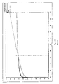
- FIG. 2 shows the operational characteristics at nodes N 1 and N 2 of the circuit of FIG. 1 .
- the two trace lines in FIG. 2 represent the voltages produced at nodes N 1 and N 2 in response to the current being sourced by the respective transistors MP 1 and MP 2 .
- a stable operating point is defined. Consequently, it can be seen that the lines are coincident at zero operating current and at a current, in this particular example, of just over 3 ⁇ A, as indicated by the dashed line.
- This characteristic of having two stable operating points leads to a problem in starting the circuit. If the circuit is simply switched on then it is possible that it will simply remain in the stable zero current operating state. Consequently, the starting of these circuits can be problematic.
- the reference voltage is around 1.25V and so the supply voltage must be at least 1.25V.
- FIG. 3 shows a current-mode bandgap reference cell which is based upon the voltage-mode bandgap cell illustrated in FIG. 1 .
- a further PMOS transistor MP 3 to provide a current which is used to produce a reference voltage VREF CM across an additional resistor R 4 .
- Additional current paths are also introduced via repositioned resistors R 2 and R 3 . These additional current paths provide that the current flowing through the PMOS transistors of the current mirror has a relationship to both V Q1 and V T .
- This current-mode topology has advantages over the voltage-mode arrangement of FIG. 1 .
- the additional current paths through the repositioned resistors R 2 and R 3 result in additional stable operating points when there is no current flowing in the bipolar transistors. This is demonstrated in FIG. 4 .
- FIG. 4 shows a linear region where the current flowing from transistors MP 1 and MP 2 is flowing into the respective resistors R 3 and R 2 , before any current begins to flow in the bipolar transistors Q 1 and Q 2 .
- FIG. 5 shows a start-up circuit arrangement for a circuit such as that shown in FIG. 3 .
- the circuit uses a PMOS transistor MP 4 to feed current directly into node N 1 .
- node N 1 When the circuit is initially powered on, there is no current flowing in the voltage reference cell formed by the transistors MP 1 , MP 2 , Q 1 , Q 2 and resistors R 1 , R 2 , R 3 and the amplifier A 1 . Node N 1 will thus be close to VSS.
- the additional bipolar transistor Q 3 and the two resistors R 6 , R 7 in conjunction with the current source CS 2 generate a coarse voltage reference VC.
- This coarse reference voltage VC is compared, using a comparator C 1 , with the output reference voltage VREF CM . Whilst the voltage reference cell is not operating at the desired operating point, the current through MP 1 , MP 2 and hence MP 3 will be low. As a result, the voltage generated across R 4 , VREF CM , will be lower than the desired output. Whilst VC is greater than VREF CM , the comparator C 1 keeps transistor MN5 turned on, which in turn, turns on the transistor MP 4 so as to provide current into node N 1 .
- the start-up circuit continues to operate until the output VREF CM exceeds some predetermined threshold.
- this circuit fails to link the operating point of the additional bipolar transistor Q 3 to the operating point of the bipolar transistors Q 1 and Q 2 in the bandgap reference cell.
- the current source biasing Q 3 does not have any feedback from the voltage reference cell. Therefore the operating conditions of Q 3 are not linked to those of Q 1 and Q 2 . That means that even if Q 3 is biased properly, there is a possibility that Q 1 and Q 2 are not. Thus again, the circuit does not reliably guarantee start-up.
- the circuit described above provides a way of providing a start-up capability to the bandgap reference cell, but in the example above the proper start-up of the voltage reference is not guaranteed. There is therefore a need for a start-up circuit which is better able to ensure that the bandgap reference cell has started operating correctly and is at or tending towards the desired operating point under all circumstances.
- FIG. 6 shows a section of a substrate showing how a bipolar transistor is typically formed in such a substrate.
- a well of N-type material is produced in the P-type substrate.
- a P-type region is then formed in the N-type well.
- the adjacent PNP layers form a parasitic PNP bipolar device which can be used as the basis for a bandgap reference circuit.
- the collector of the transistor is formed by the substrate, it is difficult to measure the device collector current. Current flowing through the bipolar device passes into the substrate and so cannot be differentiated from other currents flowing into the substrate without isolating the bipolar collector from the rest of the substrate. Additionally, measuring the current through the bipolar device is difficult without disturbing the operation of the voltage reference cell.
- a reference current generator comprising: a current generator comprising a plurality of p-n junction elements for providing said reference current; a current injector arranged to provide a control current to a first node of said current generator for increasing the magnitude of said reference current; and a comparator arranged to provide a control signal based upon comparing the difference between a first voltage derived from the voltage across one of the p-n junction elements and a second voltage proportional to the reference current, said difference being indicative of the current in said one of the p-n junctions, wherein said current injector is controlled by said control signal to provide current to said first node whilst the current in said one of the p-n junctions is below a predetermined level.
- the current generator preferably comprises a resistance element in series with one of said p-n junction elements.
- the present invention also provides a reference current generator comprising: a current generator comprising a plurality of p-n junction elements for providing said reference current; a current injector arranged to provide a control current to a first node of said current generator for increasing the magnitude of said reference current; a resistance element in series with one of said p-n junction elements; and a comparator arranged to provide a control signal based upon comparing the voltage across said resistance element to a predetermined level, said voltage being indicative of the current in said one of the p-n junctions, wherein said current injector is controlled by said control signal to provide current to said first node whilst the voltage across said resistance element is below said predetermined level.
- the p-n junction elements are provided as two separate elements.
- the first element comprises one or more p-n junctions arranged in parallel with each other.
- the second element similarly comprises one or more p-n junctions arranged in parallel with each other and including the p-n junction in series with the resistive element.
- the total emitter area of the one or more p-n junctions in said first element is preferably less than the total emitter area of the one or more p-n junctions in said second element.
- the current generator preferably comprises a current mirror arranged to provide substantially identical currents to said first element, to said second element and as the output reference current from the device.
- said first node is provided on one of said p-n junction elements to provide current to the p-n junction element.
- the current generator is preferably formed as a bandgap voltage reference circuit.
- the present invention also provides a start-up controller for a bandgap reference cell having a first voltage reference element comprising a first voltage reference device and a second voltage generating element comprising a second voltage reference device arranged in series with a resistance element, wherein said start-up controller comprises: a comparator arranged to provide a control signal by comparing the voltage on a node of said bandgap reference cell with a voltage proportional to an output reference current generated by said bandgap reference cell, said measured voltage difference corresponding to the current through one of said first or second voltage reference elements; and a current injector arranged to provide current to one of said first and second voltage reference elements whilst said measured voltage difference is below a predetermined level.
- the present invention further provides a start-up controller for a bandgap reference cell having a first voltage reference element comprising a first voltage reference device and a second voltage generating element comprising a second voltage reference device arranged in series with a resistance element, wherein said start-up controller comprises: a comparator arranged to provide a control signal by comparing the voltage across said resistance element to determine if it exceeds a predetermined value, said measured voltage difference corresponding to the current through the second voltage reference elements; and a current injector arranged to provide current to one of said first and second voltage reference elements whilst said measured voltage is below said predetermined level.
- the comparator preferably includes a predetermined offset. This means that the output only switches state when the voltage on one of the inputs exceeds the voltage on the other by the offset amount.
- the present invention additionally provides a start-up controller for a voltage reference circuit having first and second voltage reference devices, the circuit having a first stable operating state and one or more other stable operating states in which the current flowing through the first and second voltage reference devices is below a predetermined level
- the start-up controller comprising: a current monitor arranged to determine if a device current in one of said voltage reference devices is below a predetermined threshold comprising comparing a voltage proportional to the voltage across one of the first and second voltage reference devices with a voltage proportional to the output voltage of said voltage reference circuit; a current injector arranged to inject current to an injection node of said voltage reference circuit to cause the current in said voltage reference devices to increase, wherein said current injector injects current whilst said device current is determined to be below said predetermined threshold.
- the voltage proportional to the output voltage of the voltage reference circuit is preferably provided by a voltage divider arranged to provide a fixed proportion of the output voltage.
- the voltage proportional to the voltage across the one of the first and second voltage reference devices circuit is preferably provided by a voltage divider arranged to provide a fixed proportion of the voltage across the one of the first and second voltage reference devices.
- one of the first and second voltage reference devices also includes a resistance element in series with it.
- the present invention may further provide a start-up controller for a voltage reference circuit having first and second voltage reference devices, the circuit having a first stable operating state and one or more other stable operating states in which the current flowing through the first and second voltage reference devices is below a predetermined level
- the start-up controller comprising: a current monitor arranged to determine if a device current in one of said voltage reference devices is below a predetermined threshold comprising determining said device current by reference to a voltage across a resistive element in series with said one of said first and second voltage reference devices; a current injector arranged to inject current to an injection node of said voltage reference circuit to cause the current in said voltage reference device to increase, wherein said current injector injects current whilst said device current is below said predetermined threshold.
- the voltage reference devices are preferably p-n junction devices. More preferably, they are bandgap voltage reference devices.
- the voltage reference circuit may further comprise a resistance element in parallel with each of said voltage reference devices. It may additionally include a current source for producing mirrored currents to said first voltage reference device, said second voltage reference devices and a reference current output; and an amplifier arranged to control said current source to maintain the voltage across the first and second voltage reference devices at the same level.
- the present invention is embodied in an integrated circuit device.
- FIG. 1 shows a conventional voltage-mode bandgap reference cell
- FIG. 2 shows the current-to-voltage characteristics of two nodes of the bandgap reference cell of FIG. 1 ;
- FIG. 3 shows a diagram of a current-mode bandgap reference cell
- FIG. 4 shows the current-to-voltage characteristics of two nodes of the bandgap reference cell of FIG. 3 ;
- FIG. 5 shows a start-up circuit for a current-mode bandgap reference cell
- FIG. 6 shows a section of a semiconductor substrate used for forming a PNP bipolar transistor
- FIG. 7 shows a current mode bandgap reference cell with a start-up circuit according to the present invention.
- FIG. 8 shows a current mode bandgap reference cell with an alternative start-up circuit in accordance with the present invention.
- FIG. 7 shows a current-mode bandgap reference circuit with an associated start-up circuit.
- the basic bandgap reference cell is similar to those shown in the preceding examples. This consists of two bipolar transistors Q 1 and Q 2 arranged in a diode connected configuration. Transistor Q 2 is arranged to be a physically larger device than Q 1 , having an emitter area compared to that of Q 1 which is N times bigger. Transistor Q 1 connects node N 1 to the lower supply rail VSS, whereas Q 2 connects node N 2 to the lower supply rail via resistor R 1 .
- Nodes N 1 and N 2 are also connected to ground via resistors R 3 and R 2 respectively.
- resistors R 3 and R 2 are divided into pairs of resistors (R 3 a , R 3 b and R 2 a , R 2 b ) each forming a resistor divider network. This is not essential to the operation of the device and simply allows the input voltages to the amplifier A 1 to be lower than if the inputs were connected directly to the nodes N 1 and N 2 .
- the use of these resistor divider networks can be useful for lower voltage operation. However, it should be understood that the resistors R 2 a and R 3 a could be dispensed with such that the amplifier inputs were connected directly to the nodes N 1 and N 2 .
- additional resistors may be provided between node N 1 and transistor MP 1 and also between node N 2 and transistor MP 2 .
- the amplifier inputs could alternatively be connected between the resistors and the respective transistors MP 1 and MP 2 .
- transistors MP 1 and MP 2 When the bandgap reference cell starts to operate, current from transistors MP 1 and MP 2 starts to flow into nodes N 1 and N 2 respectively.
- Transistors MP 1 and MP 2 are of the same size and therefore the current into nodes N 1 and N 2 is the same. Initially, all the current flowing into nodes N 1 and N 2 passes through resistors R 3 a and R 3 b from node N 1 and R 2 a and R 2 b from node N 2 . As the current into the nodes N 1 and N 2 increases, the voltage at these nodes increases. Initially the voltage at N 1 and N 2 is lower than the base-emitter voltage of the transistors Q 1 and Q 2 and so no significant current flows through the transistors. Eventually the voltages at nodes N 1 and N 2 will be sufficiently high that the transistors Q 1 and Q 2 will start to conduct. The voltage on node N 1 will then be equivalent to the base-emitter voltage of Q 1 .
- the ratios of resistors R 3 a to R 3 b and R 2 a to R 2 b are the same. Consequently, the voltage on nodes N 3 and N 4 represent the same proportions of the voltages on nodes N 1 and N 2 .
- the amplifier A 1 operates to control the transistors MP 1 and MP 2 such that the voltages on the nodes N 3 and N 4 and hence the voltages on nodes N 1 and N 2 are the same. As a result, the voltage on node N 2 will also be the same as the base-emitter voltage of transistor Q 1 .
- the voltage across R 1 will therefore be the difference between the base-emitter voltage of Q 1 and the base-emitter voltage of Q 2 .
- V R1 V Q1 ⁇ V Q2 .
- the current (I) flowing through transistor MP 2 will be the sum of the currents flowing through resistors R 2 a and resistor R 1 :
- Current I is mirrored to the transistor MP 3 which passes through resistor R 4 to provide the current-mode voltage reference, VREF CM . The level of this voltage reference can be adjusted by adjusting the value of R 4 accordingly.
- the resistor R 4 is divided into two parts (R 4 a , R 4 b ) to form a resistor divider network in a similar way to resistors R 2 and R 3 .
- the ratio of the resistors R 4 a to R 4 b is similar to the ratio of resistors R 2 a to R 2 b in this arrangement.
- the start-up circuit is similar to the circuit described above, in that it uses a transistor MP 4 to inject current into node N 1 in order to provide current to one side (N 3 ) of the bandgap reference cell and cause the inputs to the amplifier A 1 to be offset.
- This differential input (N 3 , N 4 ) to the amplifier brings the amplifier output down low, thereby reducing the voltage on the common gate connection for the transistors MP 1 , MP 2 , MP 3 and MP 7 . This in turn increases the current into nodes N 1 and N 2 to start the process of switching the bandgap reference cell on.
- the voltage on the nodes N 4 and N 5 which provide the inputs to the comparator C 2 will be substantially the same as the lower supply rail VSS.
- the inputs to the comparator C 2 will be substantially the same.
- the comparator In order to ensure that the comparator provides a suitable output, it can be provided with an offset between its inputs. Therefore, when the input voltages to the comparator C 2 are identical, the comparator, because of the offset, operates as if it has a small negative input. This input offset results in the output of the comparator controlling the transistors MP 4 and MP 5 and pulling down their gate terminals thus causing them to turn on. This causes current to be fed into node N 1 beginning the start-up operation.
- the offset can be produced in a number of different ways such as: designing the comparator to have the offset between its terminals; or connecting a current source to provide a “trickle” current to one of the terminals.
- the current fed into node N 1 by transistor MP 4 causes the voltage on node N 1 and hence N 3 to rise. This causes an offset between the amplifier inputs since node N 4 remains substantially at the lower supply voltage VSS level since no current initially flows through MP 2 . Whilst the amplifier A 1 may have its own random offset due to fabrication variations, the difference on the inputs should be sufficiently large to overcome any such offset and so cause the amplifier to provide an output to switch on transistors MP 1 and MP 2 .
- the current through MP 2 flows to node N 2 and then through resistors R 2 a and R 2 b . Whilst the current delivered by transistor MP 2 is less than V be(Q2) /(R 2 a +R 2 b ) no current will flow through resistor R 1 into transistor Q 2 . If the start-up circuit was to be disabled at this stage, the bandgap reference cell is likely to end up at a stable but undesirable operating point, with no current flowing through the bipolar transistors.
- resistor R 4 b and resistor R 2 b are arranged to be of a similar value.
- transistors MP 2 and MP 3 are also arranged to be a similar size.
- the voltages at nodes N 4 and N 5 will be the same.
- the systematic offset in the comparator C 2 its output will continue to maintain MP 4 in conduction. This will continue to feed current into node N 1 , maintaining the offset on the voltages on nodes N 3 and N 4 .
- the arrangement of the circuit of FIG. 7 is such that the voltage difference between nodes N 4 and N 5 corresponds to the current flowing through transistor Q 2 multiplied by the resistance of resistor R 2 b.
- V N5 I.R4b
- V N4 ( I ⁇ I Q2 ).
- the comparator C 2 remains switched on until the current through transistor Q 2 is equivalent to the systematic input offset of the comparator divided by resistor R 2 b . This means that the start-up circuit only turns off after a predetermined current is flowing through the transistor Q 2 .
- the curve shows the relationship between voltage and current for the two nodes N 1 and N 2 .
- the start-up circuit turns off at a voltage below the stable operating point. This is achieved by making sure that the systematic offset of the comparator C 2 is smaller than the voltage difference between nodes N 4 and N 5 at the desired operating point. To allow for variations in the offset voltage of the comparator C 2 and the other components it should be ensured that the systematic offset of the comparator C 2 is smaller than the minimum possible voltage difference between the nodes N 4 and N 5 at the desired operating point.
- the voltage VREF CM and hence the voltage at node N 5 will be independent of temperature.
- the voltage on node N 4 is proportional to the voltage on node N 2 which, due to the amplifier A 1 , is equivalent to the voltage on node N 1 which relates to the voltage V Q1 .
- Voltage V Q1 has a negative temperature coefficient. Therefore, as the temperature of the circuit rises, the voltage difference between N 4 and N 5 will increase and hence the minimum voltage difference between nodes N 4 and N 5 will occur at the minimum operating temperature of the bandgap reference cell.
- the above-described circuit provides a start-up current to bring the bipolar transistors Q 1 , Q 2 of the bandgap reference cell into conduction and then bring the bandgap reference cell close to the desired stable operating point.
- the start-up circuit switches off. Consequently, the start-up circuit only switches off after the bipolar transistors Q 1 , Q 2 of the bandgap reference cell have begun to conduct but before the stable operating point is reached. This ensures reliable start-up of the bandgap reference cell whilst ensuring that the start-up circuit turns off correctly to ensure proper operation of the voltage reference circuit.
- the inverting input of the comparator C 2 is connected to node N 4 .
- the inverting input of the comparator could be connected to node N 3 .
- the ratio of resistors R 4 a to R 4 b is not limited to any particular value and node N 5 could be connected directly to the output VREF CM .
- the node N 5 could even be connected to a higher voltage than VREF CM where a resistor is provided between the output of VREF CM and the drain of transistor MP 3 .
- transistor MP 7 provides a bias current to the amplifier A 1 .
- the transistor MP 5 is turned on to provide a bias current to the amplifier A 1 .
- the amplifier A 1 as well as the comparator C 2 may be self-biased or receive their bias from different circuits.
- FIG. 8 An alternative arrangement of the start-up circuit will now be described by reference to FIG. 8 .
- the bandgap reference cell shown in FIG. 8 is slightly different to that shown in FIG. 7 in that resistors R 2 and R 3 are not divided into two parts and the nodes N 3 and N 4 are connected directly to the nodes N 1 and N 2 , respectively. Additionally, the comparator C 2 is connected between node N 2 and node N 6 which lies between the emitter junction of the transistor Q 2 and the resistor R 1 .
- the comparator inputs monitor the voltage across the resistor R 1 .
- the voltage across R 1 is zero and so the voltage difference between the inputs of the comparator C 2 is also zero.
- the comparator C 2 again has a systematic input offset which means that the output of the comparator is low in order to switch on transistors MP 4 and MP 5 .
- the circuit then operates in a similar manner to that of FIG. 7 with the current through MP 4 being fed into node N 1 causing the voltage at node N 1 to rise and turning on the amplifier A 1 to bring transistors MP 1 and MP 2 into conduction.
- This thermal voltage has a positive temperature coefficient and so will be at a minimum when the circuit is at the minimum operating temperature. Consequently, the minimum voltage between N 2 and N 6 will occur when the circuit is operating at the minimum operating temperature.
- the systematic input offset of the comparator C 2 will be selected according to component tolerances for the minimum operating temperature of the device.
- FIG. 8 again provides a bias current for the amplifier A 1 .
- MP 5 provides an initial bias current by the start-up circuit which is replaced by the bias current provided by MP 7 when the bandgap reference is operating normally.
- the amplifier A 1 as well as the comparator C 2 may be self-biased or receive their bias from different circuits.
- transistors Q 1 and Q 2 in the embodiments described above are shown and described as bipolar transistors. However, it will be understood that these are equivalent to and can be replaced by forward biased diodes.
- the above embodiments operate to start up the voltage cell reference by introducing additional current into the node N 1 using transistor MP 4 .
Abstract
Description
where: VQ1−VQ2=VT·ln(N); VT=k·T/q; k is Boltzmann's constant; T is the absolute temperature in degrees Kelvin; and q is the magnitude of electronic charge.
VR1=VQ1−VQ2.
VR1 has a positive temperature coefficient whereas VQ1 has a negative temperature coefficient. Current I is mirrored to the transistor MP3 which passes through resistor R4 to provide the current-mode voltage reference, VREFCM. The level of this voltage reference can be adjusted by adjusting the value of R4 accordingly. In this arrangement, the resistor R4 is divided into two parts (R4 a, R4 b) to form a resistor divider network in a similar way to resistors R2 and R3. The ratio of the resistors R4 a to R4 b is similar to the ratio of resistors R2 a to R2 b in this arrangement.
VN5=I.R4b
VN4=(I−I Q2).R2b
ΔV=VN5−VN4 =I.R4b−(I−I Q2).R2b
As R2b=R4b,
ΔV=IQ2.R2b
Claims (36)
Applications Claiming Priority (2)
| Application Number | Priority Date | Filing Date | Title |
|---|---|---|---|
| GB0619827A GB2442494A (en) | 2006-10-06 | 2006-10-06 | Voltage reference start-up circuit |
| GB0619827.9 | 2006-10-06 |
Publications (2)
| Publication Number | Publication Date |
|---|---|
| US20080224682A1 US20080224682A1 (en) | 2008-09-18 |
| US7626374B2 true US7626374B2 (en) | 2009-12-01 |
Family
ID=37454147
Family Applications (1)
| Application Number | Title | Priority Date | Filing Date |
|---|---|---|---|
| US11/902,025 Expired - Fee Related US7626374B2 (en) | 2006-10-06 | 2007-09-18 | Voltage reference circuit |
Country Status (2)
| Country | Link |
|---|---|
| US (1) | US7626374B2 (en) |
| GB (1) | GB2442494A (en) |
Cited By (20)
| Publication number | Priority date | Publication date | Assignee | Title |
|---|---|---|---|---|
| US20080007244A1 (en) * | 2006-07-07 | 2008-01-10 | Dieter Draxelmayr | Electronic Circuits and Methods for Starting Up a Bandgap Reference Circuit |
| US20100052644A1 (en) * | 2008-08-26 | 2010-03-04 | Elpida Memory Inc. | Bandgap reference circuit and method of starting bandgap reference circuit |
| US20110148389A1 (en) * | 2009-10-23 | 2011-06-23 | Rochester Institute Of Technology | Stable voltage reference circuits with compensation for non-negligible input current and methods thereof |
| US20120001613A1 (en) * | 2010-07-01 | 2012-01-05 | Conexant Systems, Inc. | High-bandwidth linear current mirror |
| RU2447477C1 (en) * | 2011-04-01 | 2012-04-10 | Государственное образовательное учреждение высшего профессионального образования "Южно-Российский государственный университет экономики и сервиса" (ГОУ ВПО "ЮРГУЭС") | Reference-voltage source |
| RU2461864C1 (en) * | 2011-06-27 | 2012-09-20 | Федеральное государственное образовательное учреждение высшего профессионального образования "Южно-Российский государственный университет экономики и сервиса" (ФГБОУ ВПО "ЮРГУЭС") | Source of reference voltage |
| US20120313665A1 (en) * | 2011-06-10 | 2012-12-13 | Ramtron International Corporation | Bandgap ready circuit |
| RU2480810C1 (en) * | 2012-02-15 | 2013-04-27 | Федеральное государственное бюджетное образовательное учреждение высшего профессионального образования "Южно-Российский государственный университет экономики и сервиса" (ФГБОУ ВПО "ЮРГУЭС") | Source of reference voltage of negative polarity |
| US20130249527A1 (en) * | 2010-02-12 | 2013-09-26 | Texas Instruments Incorporated | Electronic Device and Method for Generating a Curvature Compensated Bandgap Reference Voltage |
| RU2518974C2 (en) * | 2012-10-04 | 2014-06-10 | Федеральное государственное бюджетное образовательное учреждение высшего профессионального образования "Южно-Российский государственный университет экономики и сервиса" (ФГБОУ ВПО "ЮРГУЭС") | Source of reference voltage |
| US20140232453A1 (en) * | 2013-02-20 | 2014-08-21 | Samsung Electronics Co., Ltd. | Circuit for generating reference voltage |
| CN104076853A (en) * | 2014-05-29 | 2014-10-01 | 北京航天自动控制研究所 | Constant-current source circuit |
| US20150048879A1 (en) * | 2013-08-14 | 2015-02-19 | Ili Technology Corp. | Bandgap reference voltage circuit and electronic apparatus thereof |
| US20160062385A1 (en) * | 2014-09-02 | 2016-03-03 | Infineon Technologies Ag | Generating a current with inverse supply voltage proportionality |
| US20180074532A1 (en) * | 2016-09-13 | 2018-03-15 | Freescale Semiconductor, Inc. | Reference voltage generator |
| US10152079B2 (en) * | 2015-05-08 | 2018-12-11 | Stmicroelectronics S.R.L. | Circuit arrangement for the generation of a bandgap reference voltage |
| US10401887B2 (en) | 2015-07-22 | 2019-09-03 | Hewlett Packard Enterprise Devlopment LP | Startup circuit to initialize voltage reference circuit |
| CN111610812A (en) * | 2019-02-26 | 2020-09-01 | 合肥杰发科技有限公司 | Band-gap reference power supply generation circuit and integrated circuit |
| US11068011B2 (en) * | 2019-10-30 | 2021-07-20 | Taiwan Semiconductor Manufacturing Company Ltd. | Signal generating device and method of generating temperature-dependent signal |
| EP4303690A1 (en) * | 2022-07-05 | 2024-01-10 | MEDIATEK Inc. | Bandgap circuit with adaptive start-up design |
Families Citing this family (26)
| Publication number | Priority date | Publication date | Assignee | Title |
|---|---|---|---|---|
| DE10323012B4 (en) * | 2003-05-21 | 2005-06-02 | Austriamicrosystems Ag | Programmable integrated circuit and method of programming an integrated circuit |
| EP2239645A1 (en) * | 2009-04-09 | 2010-10-13 | austriamicrosystems AG | Band gap reference circuit and method for operating a band gap reference circuit |
| CN101995899B (en) * | 2009-08-10 | 2013-04-03 | 三星半导体(中国)研究开发有限公司 | Band gap voltage reference circuit with robustness starting circuit |
| US8049549B2 (en) * | 2010-02-26 | 2011-11-01 | Freescale Semiconductor, Inc. | Delta phi generator with start-up circuit |
| CN102375470B (en) * | 2010-08-20 | 2016-02-03 | 张伟 | A kind of band gap reference voltage circuit |
| CN102419609B (en) * | 2010-09-27 | 2015-07-08 | 联咏科技股份有限公司 | Reference voltage and reference current generating circuit |
| CN103135655B (en) * | 2011-11-30 | 2014-12-10 | 上海华虹宏力半导体制造有限公司 | Starting circuit of band gap basic standard source |
| CN103425171A (en) * | 2012-05-18 | 2013-12-04 | 联咏科技股份有限公司 | Starting circuit and band gap voltage generating device |
| JP2014086000A (en) * | 2012-10-26 | 2014-05-12 | Sony Corp | Reference voltage generation circuit |
| US9304528B2 (en) * | 2012-12-04 | 2016-04-05 | Taiwan Semiconductor Manufacturing Co., Ltd. | Reference voltage generator with op-amp buffer |
| US9780652B1 (en) | 2013-01-25 | 2017-10-03 | Ali Tasdighi Far | Ultra-low power and ultra-low voltage bandgap voltage regulator device and method thereof |
| US8723595B1 (en) * | 2013-02-19 | 2014-05-13 | Issc Technologies Corp. | Voltage generator |
| US9519304B1 (en) | 2014-07-10 | 2016-12-13 | Ali Tasdighi Far | Ultra-low power bias current generation and utilization in current and voltage source and regulator devices |
| CN104516395B (en) * | 2014-09-11 | 2016-02-10 | 上海华虹宏力半导体制造有限公司 | Band-gap reference circuit |
| US10386879B2 (en) * | 2015-01-20 | 2019-08-20 | Taiwan Semiconductor Manufacturing Company Limited | Bandgap reference voltage circuit with a startup current generator |
| US9651980B2 (en) * | 2015-03-20 | 2017-05-16 | Texas Instruments Incorporated | Bandgap voltage generation |
| US10234889B2 (en) * | 2015-11-24 | 2019-03-19 | Texas Instruments Incorporated | Low voltage current mode bandgap circuit and method |
| US9600013B1 (en) * | 2016-06-15 | 2017-03-21 | Elite Semiconductor Memory Technology Inc. | Bandgap reference circuit |
| US10203715B2 (en) * | 2016-07-27 | 2019-02-12 | Elite Semiconductor Memory Technology Inc. | Bandgap reference circuit for providing a stable reference voltage at a lower voltage level |
| CN106168826B (en) * | 2016-09-23 | 2017-06-06 | 厦门新页微电子技术有限公司 | A kind of gap tunable reference voltage circuit for being applied to wireless charging control chip |
| GB2557275A (en) * | 2016-12-02 | 2018-06-20 | Nordic Semiconductor Asa | Reference voltages |
| CN108693910A (en) * | 2017-04-11 | 2018-10-23 | 段遵虎 | A kind of programmable power supply including reference voltage circuit |
| CN107943182B (en) * | 2017-11-30 | 2019-10-11 | 上海华虹宏力半导体制造有限公司 | Band gap reference start-up circuit |
| CN107992144B (en) * | 2018-01-25 | 2019-10-11 | 上海华虹宏力半导体制造有限公司 | The start-up circuit of band gap reference |
| US11867571B2 (en) * | 2021-10-01 | 2024-01-09 | Nxp B.V. | Self-turn-on temperature detector circuit |
| CN115469708A (en) * | 2022-11-15 | 2022-12-13 | 英彼森半导体(珠海)有限公司 | Band gap reference starting circuit |
Citations (10)
| Publication number | Priority date | Publication date | Assignee | Title |
|---|---|---|---|---|
| US6150872A (en) * | 1998-08-28 | 2000-11-21 | Lucent Technologies Inc. | CMOS bandgap voltage reference |
| US6160391A (en) | 1997-07-29 | 2000-12-12 | Kabushiki Kaisha Toshiba | Reference voltage generation circuit and reference current generation circuit |
| JP2003263232A (en) | 2002-03-12 | 2003-09-19 | Asahi Kasei Microsystems Kk | Band gap reference circuit |
| US6710641B1 (en) | 2001-08-28 | 2004-03-23 | Lattice Semiconductor Corp. | Bandgap reference circuit for improved start-up |
| US6784652B1 (en) | 2003-02-25 | 2004-08-31 | National Semiconductor Corporation | Startup circuit for bandgap voltage reference generator |
| US6906581B2 (en) | 2002-04-30 | 2005-06-14 | Realtek Semiconductor Corp. | Fast start-up low-voltage bandgap voltage reference circuit |
| US6998902B2 (en) * | 2001-10-26 | 2006-02-14 | Oki Electric Industry Co., Ltd. | Bandgap reference voltage circuit |
| US7148672B1 (en) | 2005-03-16 | 2006-12-12 | Zilog, Inc. | Low-voltage bandgap reference circuit with startup control |
| US7224209B2 (en) * | 2005-03-03 | 2007-05-29 | Etron Technology, Inc. | Speed-up circuit for initiation of proportional to absolute temperature biasing circuits |
| US7531999B2 (en) * | 2005-10-27 | 2009-05-12 | Realtek Semiconductor Corp. | Startup circuit and startup method for bandgap voltage generator |
-
2006
- 2006-10-06 GB GB0619827A patent/GB2442494A/en not_active Withdrawn
-
2007
- 2007-09-18 US US11/902,025 patent/US7626374B2/en not_active Expired - Fee Related
Patent Citations (10)
| Publication number | Priority date | Publication date | Assignee | Title |
|---|---|---|---|---|
| US6160391A (en) | 1997-07-29 | 2000-12-12 | Kabushiki Kaisha Toshiba | Reference voltage generation circuit and reference current generation circuit |
| US6150872A (en) * | 1998-08-28 | 2000-11-21 | Lucent Technologies Inc. | CMOS bandgap voltage reference |
| US6710641B1 (en) | 2001-08-28 | 2004-03-23 | Lattice Semiconductor Corp. | Bandgap reference circuit for improved start-up |
| US6998902B2 (en) * | 2001-10-26 | 2006-02-14 | Oki Electric Industry Co., Ltd. | Bandgap reference voltage circuit |
| JP2003263232A (en) | 2002-03-12 | 2003-09-19 | Asahi Kasei Microsystems Kk | Band gap reference circuit |
| US6906581B2 (en) | 2002-04-30 | 2005-06-14 | Realtek Semiconductor Corp. | Fast start-up low-voltage bandgap voltage reference circuit |
| US6784652B1 (en) | 2003-02-25 | 2004-08-31 | National Semiconductor Corporation | Startup circuit for bandgap voltage reference generator |
| US7224209B2 (en) * | 2005-03-03 | 2007-05-29 | Etron Technology, Inc. | Speed-up circuit for initiation of proportional to absolute temperature biasing circuits |
| US7148672B1 (en) | 2005-03-16 | 2006-12-12 | Zilog, Inc. | Low-voltage bandgap reference circuit with startup control |
| US7531999B2 (en) * | 2005-10-27 | 2009-05-12 | Realtek Semiconductor Corp. | Startup circuit and startup method for bandgap voltage generator |
Non-Patent Citations (6)
| Title |
|---|
| A. Boni, "Op-Amps and Start-up Circuits for CMOS Bandgap References With Near 1-V Supply," IEEE J. Solid-State Circuits, vol. 37, pp. 1339-1343, Oct. 2002. |
| A. Pierazzi et al., "Band-Gap References for near 1-V operation in standard CMOS technology," IEEE 2001 Custom Integrated Circuit Conference, pp. 463-466, 2001. |
| H. Banba et al., "A CMOS Bandgap Reference Circuit with Sub-1-V Operation" IEEE J. Solid-State Circuits, vol. 34, No. 5, May 1999. |
| K. N. Leung et al., "A Sub-1-V 15-ppm/° C. CMOS Bandgap Voltage Reference Without Requiring Low Threshold Voltage Device," IEEE J. Solid-State Circuits, vol. 37, pp. 526-530, Apr. 2002. |
| M. Waltari, et al., "Reference Voltage Driver for Low-Voltage CMOS A/D Converters," Proceedings of ICECS 2000, vol. 1, pp. 28-31, 2000. |
| P. Malcovati, et al., "Curvature-Compensated BiCMOS Bandgap with 1-V Supply Voltage," IEEE J. Solid-State Circuits, vol. 36, pp. 1076-1081, Jul. 2001. |
Cited By (34)
| Publication number | Priority date | Publication date | Assignee | Title |
|---|---|---|---|---|
| US7911195B2 (en) * | 2006-07-07 | 2011-03-22 | Infineon Technologies Ag | Electronic circuits and methods for starting up a bandgap reference circuit |
| US20080007244A1 (en) * | 2006-07-07 | 2008-01-10 | Dieter Draxelmayr | Electronic Circuits and Methods for Starting Up a Bandgap Reference Circuit |
| US8294449B2 (en) * | 2008-08-26 | 2012-10-23 | Elpida Memory, Inc. | Bandgap reference circuit and method of starting bandgap reference circuit |
| US20100052644A1 (en) * | 2008-08-26 | 2010-03-04 | Elpida Memory Inc. | Bandgap reference circuit and method of starting bandgap reference circuit |
| US8653806B2 (en) | 2008-08-26 | 2014-02-18 | Elpida Memory, Inc. | Bandgap reference circuit and method of starting bandgap reference circuit |
| US20110148389A1 (en) * | 2009-10-23 | 2011-06-23 | Rochester Institute Of Technology | Stable voltage reference circuits with compensation for non-negligible input current and methods thereof |
| US9310825B2 (en) | 2009-10-23 | 2016-04-12 | Rochester Institute Of Technology | Stable voltage reference circuits with compensation for non-negligible input current and methods thereof |
| US9372496B2 (en) * | 2010-02-12 | 2016-06-21 | Texas Instruments Incorporated | Electronic device and method for generating a curvature compensated bandgap reference voltage |
| US20150331439A1 (en) * | 2010-02-12 | 2015-11-19 | Texas Instruments Incorporated | Electronic Device and Method for Generating a Curvature Compensated Bandgap Reference Voltage |
| US9104217B2 (en) * | 2010-02-12 | 2015-08-11 | Texas Instruments Incorporated | Electronic device and method for generating a curvature compensated bandgap reference voltage |
| US20130249527A1 (en) * | 2010-02-12 | 2013-09-26 | Texas Instruments Incorporated | Electronic Device and Method for Generating a Curvature Compensated Bandgap Reference Voltage |
| US8587287B2 (en) * | 2010-07-01 | 2013-11-19 | Conexant Systems, Inc. | High-bandwidth linear current mirror |
| US20120001613A1 (en) * | 2010-07-01 | 2012-01-05 | Conexant Systems, Inc. | High-bandwidth linear current mirror |
| RU2447477C1 (en) * | 2011-04-01 | 2012-04-10 | Государственное образовательное учреждение высшего профессионального образования "Южно-Российский государственный университет экономики и сервиса" (ГОУ ВПО "ЮРГУЭС") | Reference-voltage source |
| US8823267B2 (en) * | 2011-06-10 | 2014-09-02 | Cypress Semiconductor Corporation | Bandgap ready circuit |
| US20120313665A1 (en) * | 2011-06-10 | 2012-12-13 | Ramtron International Corporation | Bandgap ready circuit |
| RU2461864C1 (en) * | 2011-06-27 | 2012-09-20 | Федеральное государственное образовательное учреждение высшего профессионального образования "Южно-Российский государственный университет экономики и сервиса" (ФГБОУ ВПО "ЮРГУЭС") | Source of reference voltage |
| RU2480810C1 (en) * | 2012-02-15 | 2013-04-27 | Федеральное государственное бюджетное образовательное учреждение высшего профессионального образования "Южно-Российский государственный университет экономики и сервиса" (ФГБОУ ВПО "ЮРГУЭС") | Source of reference voltage of negative polarity |
| RU2518974C2 (en) * | 2012-10-04 | 2014-06-10 | Федеральное государственное бюджетное образовательное учреждение высшего профессионального образования "Южно-Российский государственный университет экономики и сервиса" (ФГБОУ ВПО "ЮРГУЭС") | Source of reference voltage |
| US20140232453A1 (en) * | 2013-02-20 | 2014-08-21 | Samsung Electronics Co., Ltd. | Circuit for generating reference voltage |
| US9035694B2 (en) * | 2013-02-20 | 2015-05-19 | Samsung Electronics Co., Ltd. | Circuit for generating reference voltage |
| US20150048879A1 (en) * | 2013-08-14 | 2015-02-19 | Ili Technology Corp. | Bandgap reference voltage circuit and electronic apparatus thereof |
| CN104076853A (en) * | 2014-05-29 | 2014-10-01 | 北京航天自动控制研究所 | Constant-current source circuit |
| US20160062385A1 (en) * | 2014-09-02 | 2016-03-03 | Infineon Technologies Ag | Generating a current with inverse supply voltage proportionality |
| US9785179B2 (en) * | 2014-09-02 | 2017-10-10 | Infineon Technologies Ag | Generating a current with inverse supply voltage proportionality |
| US10152079B2 (en) * | 2015-05-08 | 2018-12-11 | Stmicroelectronics S.R.L. | Circuit arrangement for the generation of a bandgap reference voltage |
| US10678289B2 (en) * | 2015-05-08 | 2020-06-09 | Stmicroelectronics S.R.L. | Circuit arrangement for the generation of a bandgap reference voltage |
| US11036251B2 (en) * | 2015-05-08 | 2021-06-15 | Stmicroelectronics S.R.L. | Circuit arrangement for the generation of a bandgap reference voltage |
| US10401887B2 (en) | 2015-07-22 | 2019-09-03 | Hewlett Packard Enterprise Devlopment LP | Startup circuit to initialize voltage reference circuit |
| US20180074532A1 (en) * | 2016-09-13 | 2018-03-15 | Freescale Semiconductor, Inc. | Reference voltage generator |
| CN111610812A (en) * | 2019-02-26 | 2020-09-01 | 合肥杰发科技有限公司 | Band-gap reference power supply generation circuit and integrated circuit |
| CN111610812B (en) * | 2019-02-26 | 2022-08-30 | 武汉杰开科技有限公司 | Band-gap reference power supply generation circuit and integrated circuit |
| US11068011B2 (en) * | 2019-10-30 | 2021-07-20 | Taiwan Semiconductor Manufacturing Company Ltd. | Signal generating device and method of generating temperature-dependent signal |
| EP4303690A1 (en) * | 2022-07-05 | 2024-01-10 | MEDIATEK Inc. | Bandgap circuit with adaptive start-up design |
Also Published As
| Publication number | Publication date |
|---|---|
| US20080224682A1 (en) | 2008-09-18 |
| GB0619827D0 (en) | 2006-11-15 |
| GB2442494A (en) | 2008-04-09 |
Similar Documents
| Publication | Publication Date | Title |
|---|---|---|
| US7626374B2 (en) | Voltage reference circuit | |
| US7789558B2 (en) | Thermal sensing circuit using bandgap voltage reference generators without trimming circuitry | |
| US10152078B2 (en) | Semiconductor device having voltage generation circuit | |
| US7944195B2 (en) | Start-up circuit for reference voltage generation circuit | |
| US7151365B2 (en) | Constant voltage generator and electronic equipment using the same | |
| US8513938B2 (en) | Reference voltage circuit and semiconductor integrated circuit | |
| US7944283B2 (en) | Reference bias generating circuit | |
| US10296026B2 (en) | Low noise reference voltage generator and load regulator | |
| US7659705B2 (en) | Low-power start-up circuit for bandgap reference voltage generator | |
| US20080157746A1 (en) | Bandgap Reference Circuits | |
| US7535285B2 (en) | Band-gap voltage reference circuit | |
| US9436205B2 (en) | Apparatus and method for low voltage reference and oscillator | |
| US20120326697A1 (en) | Temperature Independent Reference Circuit | |
| US8269478B2 (en) | Two-terminal voltage regulator with current-balancing current mirror | |
| US9110485B2 (en) | Band-gap voltage reference circuit having multiple branches | |
| JPH02183126A (en) | Temperature threshold detecting circuit | |
| JPH1145125A (en) | Reference voltage generating circuit and reference current generating circuit | |
| US10222817B1 (en) | Method and circuit for low voltage current-mode bandgap | |
| JP2007060544A (en) | Method and apparatus for producing power on reset having small temperature coefficient | |
| US7456679B2 (en) | Reference circuit and method for generating a reference signal from a reference circuit | |
| US7944272B2 (en) | Constant current circuit | |
| US7157893B2 (en) | Temperature independent reference voltage generator | |
| US6392470B1 (en) | Bandgap reference voltage startup circuit | |
| US20080106326A1 (en) | Reference voltage circuit and method for providing a reference voltage | |
| US20050046406A1 (en) | Process insensitive voltage reference |
Legal Events
| Date | Code | Title | Description |
|---|---|---|---|
| AS | Assignment |
Owner name: WOLFSON MICROELECTRONICS PIC, UNITED KINGDOM Free format text: ASSIGNMENT OF ASSIGNORS INTEREST;ASSIGNOR:HAIPLIK, HOLGER;REEL/FRAME:019902/0582 Effective date: 20070903 |
|
| STCF | Information on status: patent grant |
Free format text: PATENTED CASE |
|
| FEPP | Fee payment procedure |
Free format text: PAT HOLDER NO LONGER CLAIMS SMALL ENTITY STATUS, ENTITY STATUS SET TO UNDISCOUNTED (ORIGINAL EVENT CODE: STOL); ENTITY STATUS OF PATENT OWNER: LARGE ENTITY |
|
| FPAY | Fee payment |
Year of fee payment: 4 |
|
| AS | Assignment |
Owner name: CIRRUS LOGIC INTERNATIONAL (UK) LTD., UNITED KINGD Free format text: CHANGE OF NAME;ASSIGNOR:WOLFSON MICROELECTRONICS LTD;REEL/FRAME:035353/0413 Effective date: 20141127 Owner name: WOLFSON MICROELECTRONICS LTD, UNITED KINGDOM Free format text: CHANGE OF NAME;ASSIGNOR:WOLFSON MICROELECTRONICS PLC;REEL/FRAME:035356/0096 Effective date: 20140821 |
|
| AS | Assignment |
Owner name: CIRRUS LOGIC INTERNATIONAL SEMICONDUCTOR LTD., UNI Free format text: ASSIGNMENT OF ASSIGNORS INTEREST;ASSIGNOR:CIRRUS LOGIC INTERNATIONAL (UK) LTD.;REEL/FRAME:035806/0389 Effective date: 20150329 |
|
| AS | Assignment |
Owner name: CIRRUS LOGIC INC., TEXAS Free format text: ASSIGNMENT OF ASSIGNORS INTEREST;ASSIGNOR:CIRRUS LOGIC INTERNATIONAL SEMICONDUCTOR LTD.;REEL/FRAME:035909/0190 Effective date: 20150329 |
|
| FPAY | Fee payment |
Year of fee payment: 8 |
|
| FEPP | Fee payment procedure |
Free format text: MAINTENANCE FEE REMINDER MAILED (ORIGINAL EVENT CODE: REM.); ENTITY STATUS OF PATENT OWNER: LARGE ENTITY |
|
| LAPS | Lapse for failure to pay maintenance fees |
Free format text: PATENT EXPIRED FOR FAILURE TO PAY MAINTENANCE FEES (ORIGINAL EVENT CODE: EXP.); ENTITY STATUS OF PATENT OWNER: LARGE ENTITY |
|
| STCH | Information on status: patent discontinuation |
Free format text: PATENT EXPIRED DUE TO NONPAYMENT OF MAINTENANCE FEES UNDER 37 CFR 1.362 |
|
| FP | Lapsed due to failure to pay maintenance fee |
Effective date: 20211201 |