US7653370B2 - Offset signal phasing for a multiple frequency source system - Google Patents
Offset signal phasing for a multiple frequency source system Download PDFInfo
- Publication number
- US7653370B2 US7653370B2 US11/461,533 US46153306A US7653370B2 US 7653370 B2 US7653370 B2 US 7653370B2 US 46153306 A US46153306 A US 46153306A US 7653370 B2 US7653370 B2 US 7653370B2
- Authority
- US
- United States
- Prior art keywords
- phase
- input signal
- signal
- frequency source
- delayed
- Prior art date
- Legal status (The legal status is an assumption and is not a legal conclusion. Google has not performed a legal analysis and makes no representation as to the accuracy of the status listed.)
- Expired - Fee Related, expires
Links
Images


Classifications
-
- H—ELECTRICITY
- H03—ELECTRONIC CIRCUITRY
- H03J—TUNING RESONANT CIRCUITS; SELECTING RESONANT CIRCUITS
- H03J5/00—Discontinuous tuning; Selecting predetermined frequencies; Selecting frequency bands with or without continuous tuning in one or more of the bands, e.g. push-button tuning, turret tuner
- H03J5/24—Discontinuous tuning; Selecting predetermined frequencies; Selecting frequency bands with or without continuous tuning in one or more of the bands, e.g. push-button tuning, turret tuner with a number of separate pretuned tuning circuits or separate tuning elements selectively brought into circuit, e.g. for waveband selection or for television channel selection
- H03J5/242—Discontinuous tuning; Selecting predetermined frequencies; Selecting frequency bands with or without continuous tuning in one or more of the bands, e.g. push-button tuning, turret tuner with a number of separate pretuned tuning circuits or separate tuning elements selectively brought into circuit, e.g. for waveband selection or for television channel selection used exclusively for band selection
- H03J5/244—Discontinuous tuning; Selecting predetermined frequencies; Selecting frequency bands with or without continuous tuning in one or more of the bands, e.g. push-button tuning, turret tuner with a number of separate pretuned tuning circuits or separate tuning elements selectively brought into circuit, e.g. for waveband selection or for television channel selection used exclusively for band selection using electronic means
-
- H—ELECTRICITY
- H03—ELECTRONIC CIRCUITRY
- H03J—TUNING RESONANT CIRCUITS; SELECTING RESONANT CIRCUITS
- H03J3/00—Continuous tuning
-
- G—PHYSICS
- G06—COMPUTING; CALCULATING OR COUNTING
- G06F—ELECTRIC DIGITAL DATA PROCESSING
- G06F1/00—Details not covered by groups G06F3/00 - G06F13/00 and G06F21/00
- G06F1/04—Generating or distributing clock signals or signals derived directly therefrom
- G06F1/06—Clock generators producing several clock signals
-
- H—ELECTRICITY
- H03—ELECTRONIC CIRCUITRY
- H03J—TUNING RESONANT CIRCUITS; SELECTING RESONANT CIRCUITS
- H03J1/00—Details of adjusting, driving, indicating, or mechanical control arrangements for resonant circuits in general
- H03J1/0008—Details of adjusting, driving, indicating, or mechanical control arrangements for resonant circuits in general using a central processing unit, e.g. a microprocessor
- H03J1/0041—Details of adjusting, driving, indicating, or mechanical control arrangements for resonant circuits in general using a central processing unit, e.g. a microprocessor for frequency synthesis with counters or frequency dividers
- H03J1/005—Details of adjusting, driving, indicating, or mechanical control arrangements for resonant circuits in general using a central processing unit, e.g. a microprocessor for frequency synthesis with counters or frequency dividers in a loop
-
- H—ELECTRICITY
- H03—ELECTRONIC CIRCUITRY
- H03J—TUNING RESONANT CIRCUITS; SELECTING RESONANT CIRCUITS
- H03J3/00—Continuous tuning
- H03J3/24—Continuous tuning of more than one resonant circuit simultaneously, the circuits being tuned to substantially the same frequency, e.g. for single-knob tuning
-
- H—ELECTRICITY
- H03—ELECTRONIC CIRCUITRY
- H03L—AUTOMATIC CONTROL, STARTING, SYNCHRONISATION, OR STABILISATION OF GENERATORS OF ELECTRONIC OSCILLATIONS OR PULSES
- H03L7/00—Automatic control of frequency or phase; Synchronisation
- H03L7/06—Automatic control of frequency or phase; Synchronisation using a reference signal applied to a frequency- or phase-locked loop
- H03L7/08—Details of the phase-locked loop
- H03L7/085—Details of the phase-locked loop concerning mainly the frequency- or phase-detection arrangement including the filtering or amplification of its output signal
- H03L7/089—Details of the phase-locked loop concerning mainly the frequency- or phase-detection arrangement including the filtering or amplification of its output signal the phase or frequency detector generating up-down pulses
- H03L7/0891—Details of the phase-locked loop concerning mainly the frequency- or phase-detection arrangement including the filtering or amplification of its output signal the phase or frequency detector generating up-down pulses the up-down pulses controlling source and sink current generators, e.g. a charge pump
-
- H—ELECTRICITY
- H03—ELECTRONIC CIRCUITRY
- H03L—AUTOMATIC CONTROL, STARTING, SYNCHRONISATION, OR STABILISATION OF GENERATORS OF ELECTRONIC OSCILLATIONS OR PULSES
- H03L7/00—Automatic control of frequency or phase; Synchronisation
- H03L7/06—Automatic control of frequency or phase; Synchronisation using a reference signal applied to a frequency- or phase-locked loop
- H03L7/08—Details of the phase-locked loop
- H03L7/085—Details of the phase-locked loop concerning mainly the frequency- or phase-detection arrangement including the filtering or amplification of its output signal
- H03L7/093—Details of the phase-locked loop concerning mainly the frequency- or phase-detection arrangement including the filtering or amplification of its output signal using special filtering or amplification characteristics in the loop
-
- H—ELECTRICITY
- H03—ELECTRONIC CIRCUITRY
- H03L—AUTOMATIC CONTROL, STARTING, SYNCHRONISATION, OR STABILISATION OF GENERATORS OF ELECTRONIC OSCILLATIONS OR PULSES
- H03L7/00—Automatic control of frequency or phase; Synchronisation
- H03L7/06—Automatic control of frequency or phase; Synchronisation using a reference signal applied to a frequency- or phase-locked loop
- H03L7/08—Details of the phase-locked loop
- H03L7/099—Details of the phase-locked loop concerning mainly the controlled oscillator of the loop
-
- H—ELECTRICITY
- H03—ELECTRONIC CIRCUITRY
- H03L—AUTOMATIC CONTROL, STARTING, SYNCHRONISATION, OR STABILISATION OF GENERATORS OF ELECTRONIC OSCILLATIONS OR PULSES
- H03L7/00—Automatic control of frequency or phase; Synchronisation
- H03L7/06—Automatic control of frequency or phase; Synchronisation using a reference signal applied to a frequency- or phase-locked loop
- H03L7/08—Details of the phase-locked loop
- H03L7/10—Details of the phase-locked loop for assuring initial synchronisation or for broadening the capture range
-
- H—ELECTRICITY
- H03—ELECTRONIC CIRCUITRY
- H03L—AUTOMATIC CONTROL, STARTING, SYNCHRONISATION, OR STABILISATION OF GENERATORS OF ELECTRONIC OSCILLATIONS OR PULSES
- H03L7/00—Automatic control of frequency or phase; Synchronisation
- H03L7/06—Automatic control of frequency or phase; Synchronisation using a reference signal applied to a frequency- or phase-locked loop
- H03L7/16—Indirect frequency synthesis, i.e. generating a desired one of a number of predetermined frequencies using a frequency- or phase-locked loop
- H03L7/18—Indirect frequency synthesis, i.e. generating a desired one of a number of predetermined frequencies using a frequency- or phase-locked loop using a frequency divider or counter in the loop
- H03L7/197—Indirect frequency synthesis, i.e. generating a desired one of a number of predetermined frequencies using a frequency- or phase-locked loop using a frequency divider or counter in the loop a time difference being used for locking the loop, the counter counting between numbers which are variable in time or the frequency divider dividing by a factor variable in time, e.g. for obtaining fractional frequency division
- H03L7/1974—Indirect frequency synthesis, i.e. generating a desired one of a number of predetermined frequencies using a frequency- or phase-locked loop using a frequency divider or counter in the loop a time difference being used for locking the loop, the counter counting between numbers which are variable in time or the frequency divider dividing by a factor variable in time, e.g. for obtaining fractional frequency division for fractional frequency division
- H03L7/1976—Indirect frequency synthesis, i.e. generating a desired one of a number of predetermined frequencies using a frequency- or phase-locked loop using a frequency divider or counter in the loop a time difference being used for locking the loop, the counter counting between numbers which are variable in time or the frequency divider dividing by a factor variable in time, e.g. for obtaining fractional frequency division for fractional frequency division using a phase accumulator for controlling the counter or frequency divider
-
- H—ELECTRICITY
- H03—ELECTRONIC CIRCUITRY
- H03L—AUTOMATIC CONTROL, STARTING, SYNCHRONISATION, OR STABILISATION OF GENERATORS OF ELECTRONIC OSCILLATIONS OR PULSES
- H03L7/00—Automatic control of frequency or phase; Synchronisation
- H03L7/06—Automatic control of frequency or phase; Synchronisation using a reference signal applied to a frequency- or phase-locked loop
- H03L7/16—Indirect frequency synthesis, i.e. generating a desired one of a number of predetermined frequencies using a frequency- or phase-locked loop
- H03L7/22—Indirect frequency synthesis, i.e. generating a desired one of a number of predetermined frequencies using a frequency- or phase-locked loop using more than one loop
- H03L7/23—Indirect frequency synthesis, i.e. generating a desired one of a number of predetermined frequencies using a frequency- or phase-locked loop using more than one loop with pulse counters or frequency dividers
-
- H—ELECTRICITY
- H03—ELECTRONIC CIRCUITRY
- H03H—IMPEDANCE NETWORKS, e.g. RESONANT CIRCUITS; RESONATORS
- H03H11/00—Networks using active elements
- H03H11/02—Multiple-port networks
- H03H11/04—Frequency selective two-port networks
- H03H11/12—Frequency selective two-port networks using amplifiers with feedback
- H03H11/1291—Current or voltage controlled filters
-
- H—ELECTRICITY
- H03—ELECTRONIC CIRCUITRY
- H03J—TUNING RESONANT CIRCUITS; SELECTING RESONANT CIRCUITS
- H03J2200/00—Indexing scheme relating to tuning resonant circuits and selecting resonant circuits
- H03J2200/10—Tuning of a resonator by means of digitally controlled capacitor bank
-
- H—ELECTRICITY
- H03—ELECTRONIC CIRCUITRY
- H03J—TUNING RESONANT CIRCUITS; SELECTING RESONANT CIRCUITS
- H03J2200/00—Indexing scheme relating to tuning resonant circuits and selecting resonant circuits
- H03J2200/17—Elimination of interference caused by harmonics of local oscillator
-
- H—ELECTRICITY
- H03—ELECTRONIC CIRCUITRY
- H03J—TUNING RESONANT CIRCUITS; SELECTING RESONANT CIRCUITS
- H03J7/00—Automatic frequency control; Automatic scanning over a band of frequencies
- H03J7/02—Automatic frequency control
- H03J7/04—Automatic frequency control where the frequency control is accomplished by varying the electrical characteristics of a non-mechanically adjustable element or where the nature of the frequency controlling element is not significant
- H03J7/06—Automatic frequency control where the frequency control is accomplished by varying the electrical characteristics of a non-mechanically adjustable element or where the nature of the frequency controlling element is not significant using counters or frequency dividers
- H03J7/065—Automatic frequency control where the frequency control is accomplished by varying the electrical characteristics of a non-mechanically adjustable element or where the nature of the frequency controlling element is not significant using counters or frequency dividers the counter or frequency divider being used in a phase locked loop
-
- H—ELECTRICITY
- H03—ELECTRONIC CIRCUITRY
- H03J—TUNING RESONANT CIRCUITS; SELECTING RESONANT CIRCUITS
- H03J7/00—Automatic frequency control; Automatic scanning over a band of frequencies
- H03J7/02—Automatic frequency control
- H03J7/04—Automatic frequency control where the frequency control is accomplished by varying the electrical characteristics of a non-mechanically adjustable element or where the nature of the frequency controlling element is not significant
- H03J7/08—Automatic frequency control where the frequency control is accomplished by varying the electrical characteristics of a non-mechanically adjustable element or where the nature of the frequency controlling element is not significant using varactors, i.e. voltage variable reactive diodes
-
- H—ELECTRICITY
- H03—ELECTRONIC CIRCUITRY
- H03L—AUTOMATIC CONTROL, STARTING, SYNCHRONISATION, OR STABILISATION OF GENERATORS OF ELECTRONIC OSCILLATIONS OR PULSES
- H03L2207/00—Indexing scheme relating to automatic control of frequency or phase and to synchronisation
- H03L2207/06—Phase locked loops with a controlled oscillator having at least two frequency control terminals
Definitions
- the present invention relates to tunable systems employing concurrently operable frequency sources, and in particular to offset signal phasing for use with said system.
- multiple frequency sources in a system presents possible challenges in how to control the system's power consumption.
- the operation of multiple frequency sources may create a high peak current demand from the power supply, possibly resulting in a drop in the power supply voltage to a level which may be insufficient to continue reliable system operation.
- the multiple frequency source system includes a first operating frequency source, a phase delay element, and a second operating frequency source configured to operate concurrently with the first frequency source.
- the first frequency source includes an input coupled to receive a reference input signal and an output for providing a first frequency source signal.
- the phase delay includes an input coupled to receive the input reference signal, and an output, the phase delay element operable to apply a predefined phase delay to the input reference signal to produce a phase-delayed input signal.
- the second frequency source includes an input coupled to receive the phase-delayed input signal and an output for providing a second frequency source signal.
- FIG. 1A illustrates a tunable system employing multiple frequency sources, whereby the operating frequency sources are operating coherently.
- FIG. 1B illustrates time domain signal waveforms and peak current consumption for the tunable multiple frequency source system of FIG. 1A .
- FIG. 2A illustrates an exemplary multiple frequency source system employing offset signal phasing in accordance with the present invention.
- FIG. 2B illustrates an exemplary method for operating a multiple frequency source system in accordance within one embodiment of the present invention.
- FIG. 2C illustrates time domain signal waveforms and peak current consumption for the system of FIG. 2A using the method of FIG. 2B
- FIG. 3 illustrates an exemplary implementation of the phase delay elements used to provide offset signal phasing in the tunable multiple frequency source system of FIG. 2A .
- FIG. 4 illustrates an exemplary block diagram of a regulated power supply for use with the tunable multiple frequency source system of FIG. 3A .
- FIG. 1A illustrates a tunable system employing concurrently operating frequency sources (“tunable multiple frequency source”), whereby the operating frequency sources are operating in a high current mode coherently.
- the system 100 includes n frequency sources 130 1,n , which in a particular embodiment, includes at least one tunable source, such a variable frequency oscillator or phase locked loop. One or more of the remaining frequency sources may be tunable or fixed frequency sources.
- the system receives an input signal 110 which is supplied to two or more (all, as illustrated) of the operating frequency sources 130 1,n .
- the input signal 110 is operable to initiate a high current mode of operation, which may comprise activating the frequency source to generate an output signal F S1,n .
- the input signal 110 may be a clock signal, a reference signal, or other such signal operable to activate the frequency sources, or to otherwise produce a high current mode of operation such that the frequency source begins to draw a significant amount of current (e.g., more than 50 percent of its maximum current handling capacity).
- FIG. 1B illustrates time domain signal waveforms and peak current consumption for the tunable multiple frequency source system of FIG. 1A .
- multiple frequency sources are activated, and accordingly, enter into a high current mode of operation substantially concurrently.
- the power supply bus is subjected to very high current supply spikes. This condition creates undesired effects, in that the power supply may not have sufficient capacity to supply the high peak current needed during these periods, resulting in a drop in the supply voltage to a level which may not be sufficient to continue reliable system operation.
- the generation of the high current spikes in the time domain is accompanied by a large number of spurious products in the frequency domain.
- FIG. 2A illustrates an exemplary tunable multiple frequency source system employing offset signal phasing in accordance with the present invention.
- the system includes n frequency sources 230 1,n operable to generate n corresponding frequency source signals F Sn , and n ⁇ 1 phase delay elements 220 1,(n ⁇ 1) .
- An input signal 210 is operable to activate, or otherwise cause the coupled frequency sources 230 1,n to enter into a high current mode.
- the n ⁇ 1 phase delay elements 220 1,n are interposed between adjacent frequency sources, wherein one of the frequency sources (illustrated as frequency source 2 , 230 2 ) receives an undelayed version of the input signal 210 (referred to herein as the reference input signal) and operates as a reference frequency source.
- Each of the n ⁇ 1 phase-delay elements 220 is operable to apply a particular predefined phase offset ⁇ 1,(n ⁇ 1) to the incoming signal, thereby producing n ⁇ 1 delayed input signals 225 .
- the calculation of the predefined phase offsets the calculation of which is further described below.
- the phase delay may be provided electrically, i.e., through the use of a particular structure such as an inverter, or physically, through the implementation of a number of cascaded elements (e.g., inverters) that provides a time delay equivalent to the desired phase delay.
- the system 200 may be implemented in “ladder” type network arrangement in which the phase delay at the input of the nth frequency source 230 n is the sum of delay elements 220 2 to 220 n .
- a “star” type network may be employed in which each delay element 2201 , 2 receives the system input signal 210 , and only one delay element is used to apply the desired delay prior to input to the corresponding frequency source 230 .
- the system may employ segments of both types of structures, as shown in the illustrated embodiment of FIG. 2A .
- FIG. 2B illustrates an exemplary method for operating a tunable multiple frequency source system in accordance within one embodiment of the present invention.
- a reference frequency source e.g. source 230 2
- the signal input into the reference frequency source is defined as having a relative phase offset of zero degrees in the following phase offset computation process.
- phase offsets for each of the remaining n ⁇ 1 signals which are input into the corresponding n ⁇ 1 frequency sources are computed.
- the reference signal, and the remaining n ⁇ 1 input signals are spaced equally apart over a phase range provided by the calculation:
- n - 1 n ⁇ 360 phase ⁇ ⁇ range eq . ⁇ ( 1 ) where n is the number of concurrently operating frequency sources.
- the reference input signal is located at 0 degrees
- the first and second phase-delayed signals are located at 120 and 240 degrees phase.
- the reference input signal and the remaining n ⁇ 1 phase-delayed signals are spaced equally apart over a 180 degree phase range.
- the reference input signal is located at 0 degrees
- the first and second phase-delayed signals are located at 90 and 180 degrees phase.
- the phase offsets computed for the respective n ⁇ 1 input signals are applied to their corresponding input signals to provide the desired phase delay.
- one or more of the n ⁇ 1 input signals are transmitted through an odd number (2n+1) of inverters cascaded to provide a 180 degree phase shift relative to an even number (2n) of cascaded inverters which may be used to provide the reference input signal.
- one or more of the n ⁇ 1 input signals are transmitted through a cascaded string of circuit elements (e.g., inverters) operable to provide a physical time delay which provides the desired phase delay.
- circuit elements e.g., inverters
- FIG. 2C illustrates time domain signal waveforms and peak current consumption for the system of FIG. 2A using the method of FIG. 2B .
- the responses are shown for a system consistent with FIG. 2A employing three concurrently operation frequency sources which provide output frequencies F S0 , F S1 and F S2 , respectively.
- the system includes a first phase delay element ⁇ 1 which generates a 180 degree phase-shifted delayed input signal 225 1 , that signal 225 1 being supplied to its corresponding frequency source 230 1 to produce an output waveform F S1 .
- a second phase delay element 100 2 which generates a 90 degree phase-shifted delayed input signal 225 2 , that signal 225 2 being supplied to its corresponding frequency source 230 3 to produce an output waveform FS 3 .
- the rising edges of F S1 , F S2 , F S3 are offset 90 degrees from each other.
- the offset phasing produces a distributed peak current response compared to the response in FIG. 1 , resulting in reduced current peaking and less spurious product generation.
- one or more of the concurrently operating frequency source 230 1,n will be a tunable source, an example of which is a sigma-delta fractional phase locked loop circuit.
- the remaining frequency sources may be tunable or fixed frequency, as dictated by the design.
- the phase-delay element associated therewith may be located along the signal path supplying the loop's reference signal F Ref .
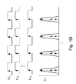
- FIG. 3 illustrates an exemplary implementation of the phase delay elements used to provide offset signal phasing in system of FIG. 2A .
- the phase delay element ⁇ 1 220 1 includes three inverter elements 310 1 , 310 2 and 310 3 , this number representing one inverter more than the total number of inverter elements 320 1 and 320 2 provided for the reference input signal 225 2 .
- the two inverter delay elements 310 1 and 310 2 are used to provide an input buffer to the input of the reference frequency source 230 2 receiving the reference input signal 225 2
- the additional inverter element 310 3 supplied in the phase delay element 220 1 provides a 180 degree phase relative to the reference input signal 225 2 .
- inverter elements may be used (e.g., no inverters used for the reference input signal 225 2 and one inverter element for producing the delayed input signal 225 1 ), or more inverter elements may be used (e.g., 2n inverters used for generating the delayed input signal 225 1 , and 2n+1 inverters used for generating the reference input signal 225 2 ).
- Phase delay element ⁇ 2 220 2 is realized in a particular embodiment using multiple, series-coupled inverter elements 330 1,m , the collective arrangement of which produces the desired time/phase delay.
- the desired delay is substantially midway between the phasing of the existing reference and delayed input signals 225 1 and 225 2 ; for example in the above illustrated embodiment in which reference and delayed input signals 225 1 and 225 2 are located at 0 and 180 degree relative phasing, a sufficient number of inverter elements 330 1,m is cascaded to provide a time/phase delay substantially equivalent to 90 degrees of phase delay.
- a cascaded arrangement of 150-200 inverter elements may be needed to provide the physical delay.
- the inverter elements are quite small in size, have high associated yield, and are easily producible, a large number can be easily implemented within an integrated circuit without difficulty.
- FIG. 4 illustrates an exemplary block diagram of a regulated power supply (“regulator” herein) for the tunable multiple frequency source system of FIG. 3A .
- the regulator 400 includes an operation amplifier OP 1 410 , a transistor T 1 420 , feedback resistors R 1 and R 2 430 , regulator capacitor C 1 440 , and a power supply bus 450 .
- the operational amplifier 410 is connected in a conventional non-inverting amplifier configuration and includes a non-inverting input coupled to receive a reference voltage and a resistive divider formed by resistors 430 a and 430 b coupled to the inverting input.
- the regulator capacitor 440 is operable to filter out ac signals propagating along the power supply bus 450 and provides charge to the power supply bus 450 when supply transistor 420 is in a cutoff mode.
- Supply transistor 420 (exemplary illustrated as a bipolar junction transistor) includes a collector terminal coupled to the unregulated power supply, a base terminal coupled to the output of the operational amplifier 410 , and an emitter terminal coupled to the power supply bus 450 .
- the supply transistor 420 and regulator capacitor 440 supplies the required current. Due to the limited bandwidth of the regulator (especially if it is providing a very low amount of DC current) the peak current is provided by the regulator capacitor 440 from the charge stored thereby, with a consequential drop of the regulated voltage. After the time delay dependent on the regulator bandwidth, the regulator restores the charge in the regulator capacitor 440 , bringing the regulated voltage to steady state value. In the low current conduction, the lower value of the peak current supplied at higher frequency acts as low pass filtering of the peak current that needs to be supplied in high current mode. Consequently the voltage ripple on the regulated voltage is reduced.
- the described processes may be implemented in hardware, software, firmware or a combination of these implementations as appropriate.
- some or all of the described processes may be implemented as computer readable instruction code resident on a computer readable medium (removable disk, volatile or non-volatile memory, embedded processors, etc.), the instruction code operable to program a computer of other such programmable device to carry out the intended functions.
Abstract
Description
where n is the number of concurrently operating frequency sources.
Claims (27)
Priority Applications (1)
| Application Number | Priority Date | Filing Date | Title |
|---|---|---|---|
| US11/461,533 US7653370B2 (en) | 2005-08-02 | 2006-08-01 | Offset signal phasing for a multiple frequency source system |
Applications Claiming Priority (4)
| Application Number | Priority Date | Filing Date | Title |
|---|---|---|---|
| US59575005P | 2005-08-02 | 2005-08-02 | |
| US59575405P | 2005-08-02 | 2005-08-02 | |
| US59574905P | 2005-08-02 | 2005-08-02 | |
| US11/461,533 US7653370B2 (en) | 2005-08-02 | 2006-08-01 | Offset signal phasing for a multiple frequency source system |
Publications (2)
| Publication Number | Publication Date |
|---|---|
| US20070176663A1 US20070176663A1 (en) | 2007-08-02 |
| US7653370B2 true US7653370B2 (en) | 2010-01-26 |
Family
ID=37467507
Family Applications (3)
| Application Number | Title | Priority Date | Filing Date |
|---|---|---|---|
| US11/461,533 Expired - Fee Related US7653370B2 (en) | 2005-08-02 | 2006-08-01 | Offset signal phasing for a multiple frequency source system |
| US11/461,530 Expired - Fee Related US7528665B2 (en) | 2005-08-02 | 2006-08-01 | Multiple frequency source system and method of operation |
| US11/461,534 Expired - Fee Related US7355483B2 (en) | 2005-08-02 | 2006-08-01 | System and method for mitigating phase pulling in a multiple frequency source system |
Family Applications After (2)
| Application Number | Title | Priority Date | Filing Date |
|---|---|---|---|
| US11/461,530 Expired - Fee Related US7528665B2 (en) | 2005-08-02 | 2006-08-01 | Multiple frequency source system and method of operation |
| US11/461,534 Expired - Fee Related US7355483B2 (en) | 2005-08-02 | 2006-08-01 | System and method for mitigating phase pulling in a multiple frequency source system |
Country Status (6)
| Country | Link |
|---|---|
| US (3) | US7653370B2 (en) |
| EP (3) | EP1911185B1 (en) |
| JP (3) | JP4245658B2 (en) |
| KR (4) | KR100917085B1 (en) |
| AT (1) | ATE535065T1 (en) |
| WO (3) | WO2007015211A2 (en) |
Cited By (1)
| Publication number | Priority date | Publication date | Assignee | Title |
|---|---|---|---|---|
| US20080143192A1 (en) * | 2006-12-14 | 2008-06-19 | Sample Alanson P | Dynamic radio frequency power harvesting |
Families Citing this family (17)
| Publication number | Priority date | Publication date | Assignee | Title |
|---|---|---|---|---|
| US7783467B2 (en) * | 2005-12-10 | 2010-08-24 | Electronics And Telecommunications Research Institute | Method for digital system modeling by using higher software simulator |
| US7474167B1 (en) * | 2006-08-31 | 2009-01-06 | Altera Corporation | Capacitance switch circuitry for digitally controlled oscillators |
| US7869781B2 (en) | 2006-12-06 | 2011-01-11 | Broadcom Corporation | Method and system for mitigating the effects of pulling in multiple phase locked loops in multi-standard systems |
| CN101197573B (en) * | 2007-01-10 | 2010-12-29 | 晨星半导体股份有限公司 | Clock pulse generator, self testing and switch control method used on the same |
| JP2009010599A (en) * | 2007-06-27 | 2009-01-15 | Panasonic Corp | Digitally controlled oscillator circuit, frequency synthesizer, radio communication device using the same and its controlling method |
| US8212610B2 (en) * | 2008-09-19 | 2012-07-03 | Altera Corporation | Techniques for digital loop filters |
| KR101467417B1 (en) * | 2008-12-30 | 2014-12-11 | 주식회사 동부하이텍 | digital synchronous circuits |
| US20100250746A1 (en) * | 2009-03-30 | 2010-09-30 | Hitachi, Ltd. | Information technology source migration |
| JP5148548B2 (en) * | 2009-04-17 | 2013-02-20 | 株式会社東芝 | Digital PLL circuit and semiconductor integrated circuit |
| WO2010134287A1 (en) * | 2009-05-22 | 2010-11-25 | パナソニック株式会社 | Pll frequency synthesizer |
| US8756451B2 (en) * | 2011-10-01 | 2014-06-17 | Intel Corporation | Frequency synthesis methods and systems |
| US8692594B2 (en) * | 2011-12-19 | 2014-04-08 | Ati Technologies Ulc | Phase-locked loop frequency stepping |
| US9166604B2 (en) * | 2012-04-25 | 2015-10-20 | Infineon Technologies Ag | Timing monitor for PLL |
| US9490825B2 (en) * | 2013-05-23 | 2016-11-08 | Intel IP Corporation | Adjusting tuning segments in a digitally-controlled oscillator |
| US9509353B2 (en) | 2014-08-20 | 2016-11-29 | Nxp B.V. | Data processing device |
| GB201800174D0 (en) * | 2018-01-05 | 2018-02-21 | Kirintec Ltd | Receiver |
| CN111508416B (en) * | 2020-04-30 | 2021-09-03 | 武汉华星光电半导体显示技术有限公司 | Display and driving method thereof |
Citations (27)
| Publication number | Priority date | Publication date | Assignee | Title |
|---|---|---|---|---|
| JPH077386A (en) | 1993-03-29 | 1995-01-10 | Philips Electron Nv | Signal receiving device |
| US5452290A (en) | 1992-10-26 | 1995-09-19 | Motorola, Inc. | Look ahead channel switching transceiver |
| US5565816A (en) | 1995-08-18 | 1996-10-15 | International Business Machines Corporation | Clock distribution network |
| JPH09246967A (en) * | 1996-03-04 | 1997-09-19 | Casio Comput Co Ltd | Pll frequency synthesizer circuit |
| US5774701A (en) * | 1995-07-10 | 1998-06-30 | Hitachi, Ltd. | Microprocessor operating at high and low clok frequencies |
| WO1999041933A1 (en) | 1998-02-12 | 1999-08-19 | Telefonaktiebolaget Lm Ericsson (Publ) | Method and device in a mobile telecommunications network |
| US6005420A (en) * | 1996-04-01 | 1999-12-21 | Kabushiki Kaisha Toshiba | Frequency multiplying circuit having a greater multiplying ratio |
| US6112308A (en) * | 1998-01-23 | 2000-08-29 | Intel Corporation | Cascaded multiple internal phase-locked loops for synchronization of hierarchically distinct chipset components and subsystems |
| EP1045606A2 (en) | 1999-04-15 | 2000-10-18 | Texas Instruments Incorporated | Method and device for a multiple access wireless communication system |
| US6147561A (en) * | 1999-07-29 | 2000-11-14 | Conexant Systems, Inc. | Phase/frequency detector with time-delayed inputs in a charge pump based phase locked loop and a method for enhancing the phase locked loop gain |
| US6177964B1 (en) * | 1997-08-01 | 2001-01-23 | Microtune, Inc. | Broadband integrated television tuner |
| US6226537B1 (en) * | 1997-05-23 | 2001-05-01 | Matsushita Electric Industrial Co., Ltd. | Portable radio device |
| US6275990B1 (en) | 1995-02-06 | 2001-08-14 | Adc Telecommunications, Inc. | Transport of payload information and control messages on multiple orthogonal carriers spread throughout substantially all of a frequency bandwith |
| US6304146B1 (en) | 1998-05-29 | 2001-10-16 | Silicon Laboratories, Inc. | Method and apparatus for synthesizing dual band high-frequency signals for wireless communications |
| US20030006850A1 (en) | 2000-04-25 | 2003-01-09 | The National University Of Singapore | Method and apparatus for a digital clock multiplication circuit |
| US20030076184A1 (en) * | 2001-10-24 | 2003-04-24 | Takeo Oita | Input-switching voltage-controlled oscillator and PLL-controlled oscillator |
| US20030109242A1 (en) * | 2001-12-10 | 2003-06-12 | Alps Electric Co., Ltd. | Receiver capable of receiving radio signals in a preferred state at all times |
| US20030179842A1 (en) * | 2002-03-22 | 2003-09-25 | Kane Michael G. | Digital pattern sequence generator |
| WO2004000822A1 (en) | 2002-06-24 | 2003-12-31 | Cj Corporation | 2-thioxothiazole derivative, method for preparing the same, and pharmaceutical composition containing the same |
| US20040012447A1 (en) * | 2002-07-16 | 2004-01-22 | Hitachi, Ltd. | Multiple PLL oscillator and multiple CW radar used therefore |
| US6686803B1 (en) * | 2000-07-10 | 2004-02-03 | Silicon Laboratories, Inc. | Integrated circuit incorporating circuitry for determining which of at least two possible frequencies is present on an externally provided reference signal and method therefor |
| US20040156465A1 (en) | 2001-01-22 | 2004-08-12 | Bernd Schmandt | Method for operating a PLL frequency synthesis circuit |
| US20040189366A1 (en) | 2003-03-27 | 2004-09-30 | Helmut Haringer | Clocking scheme and clock system for a monolithic integrated circuit |
| US7062229B2 (en) * | 2002-03-06 | 2006-06-13 | Qualcomm Incorporated | Discrete amplitude calibration of oscillators in frequency synthesizers |
| US20060153323A1 (en) * | 2004-12-24 | 2006-07-13 | Kabushiki Kaisha Toshiba | Clock generation device and clock generation method |
| US7216249B2 (en) | 2002-06-11 | 2007-05-08 | Rohm Co., Ltd. | Clock generation system |
| US7339078B2 (en) * | 1995-03-10 | 2008-03-04 | G.D. Searle Llc | Bis-amino acid hydroxyethylamino sulfonamide retroviral protease inhibitors |
Family Cites Families (12)
| Publication number | Priority date | Publication date | Assignee | Title |
|---|---|---|---|---|
| JPS6120420A (en) * | 1984-07-06 | 1986-01-29 | Nec Corp | Polyphase clock generating circuit |
| JP2541313B2 (en) * | 1989-07-29 | 1996-10-09 | 日本電気株式会社 | Dual PLL device |
| JP3453006B2 (en) * | 1995-07-07 | 2003-10-06 | パイオニア株式会社 | Phase synchronization circuit and digital signal reproducing device |
| JP3596172B2 (en) * | 1996-06-19 | 2004-12-02 | 富士通株式会社 | PLL frequency synthesizer |
| JPH10270999A (en) * | 1997-03-24 | 1998-10-09 | Seiko Epson Corp | Semiconductor device |
| JPH11205101A (en) * | 1998-01-13 | 1999-07-30 | Toshiba Corp | Phase followup device |
| US6628779B1 (en) | 1998-05-11 | 2003-09-30 | Telcordia Technologies, Inc. | Method and system for scaleable near-end speech cancellation for tip and ring tone signal detectors |
| JP2000286704A (en) * | 1999-01-28 | 2000-10-13 | Matsushita Electric Ind Co Ltd | Frequency synthesizer device and mobile radio equipment using the same |
| JP2001332969A (en) * | 2000-05-23 | 2001-11-30 | Nec Microsystems Ltd | Oscillator |
| JP4454810B2 (en) * | 2000-08-04 | 2010-04-21 | Necエレクトロニクス株式会社 | Digital phase control method and digital phase control circuit |
| US20040006850A1 (en) | 2002-07-09 | 2004-01-15 | Wax David B. | Personal pen retaining system |
| WO2004082277A1 (en) * | 2003-03-11 | 2004-09-23 | Thomson Licensing S.A. | Apparatus and method for distributing signals |
-
2006
- 2006-08-01 WO PCT/IB2006/052634 patent/WO2007015211A2/en active Application Filing
- 2006-08-01 KR KR1020087003990A patent/KR100917085B1/en not_active IP Right Cessation
- 2006-08-01 US US11/461,533 patent/US7653370B2/en not_active Expired - Fee Related
- 2006-08-01 KR KR1020097009988A patent/KR100966926B1/en not_active IP Right Cessation
- 2006-08-01 EP EP06780271A patent/EP1911185B1/en not_active Not-in-force
- 2006-08-01 US US11/461,530 patent/US7528665B2/en not_active Expired - Fee Related
- 2006-08-01 EP EP06766078A patent/EP1910908A1/en not_active Withdrawn
- 2006-08-01 KR KR1020087005222A patent/KR100967723B1/en not_active IP Right Cessation
- 2006-08-01 WO PCT/IB2006/052632 patent/WO2007015209A1/en active Application Filing
- 2006-08-01 US US11/461,534 patent/US7355483B2/en not_active Expired - Fee Related
- 2006-08-01 KR KR1020087002866A patent/KR100853047B1/en not_active IP Right Cessation
- 2006-08-01 JP JP2008524659A patent/JP4245658B2/en not_active Expired - Fee Related
- 2006-08-01 EP EP06766077A patent/EP1911159A1/en not_active Withdrawn
- 2006-08-01 AT AT06780271T patent/ATE535065T1/en active
- 2006-08-01 JP JP2008524658A patent/JP2009504064A/en active Pending
- 2006-08-01 JP JP2008524657A patent/JP4395541B2/en not_active Expired - Fee Related
- 2006-08-01 WO PCT/IB2006/052633 patent/WO2007015210A1/en active Application Filing
Patent Citations (27)
| Publication number | Priority date | Publication date | Assignee | Title |
|---|---|---|---|---|
| US5452290A (en) | 1992-10-26 | 1995-09-19 | Motorola, Inc. | Look ahead channel switching transceiver |
| JPH077386A (en) | 1993-03-29 | 1995-01-10 | Philips Electron Nv | Signal receiving device |
| US6275990B1 (en) | 1995-02-06 | 2001-08-14 | Adc Telecommunications, Inc. | Transport of payload information and control messages on multiple orthogonal carriers spread throughout substantially all of a frequency bandwith |
| US7339078B2 (en) * | 1995-03-10 | 2008-03-04 | G.D. Searle Llc | Bis-amino acid hydroxyethylamino sulfonamide retroviral protease inhibitors |
| US5774701A (en) * | 1995-07-10 | 1998-06-30 | Hitachi, Ltd. | Microprocessor operating at high and low clok frequencies |
| US5565816A (en) | 1995-08-18 | 1996-10-15 | International Business Machines Corporation | Clock distribution network |
| JPH09246967A (en) * | 1996-03-04 | 1997-09-19 | Casio Comput Co Ltd | Pll frequency synthesizer circuit |
| US6005420A (en) * | 1996-04-01 | 1999-12-21 | Kabushiki Kaisha Toshiba | Frequency multiplying circuit having a greater multiplying ratio |
| US6226537B1 (en) * | 1997-05-23 | 2001-05-01 | Matsushita Electric Industrial Co., Ltd. | Portable radio device |
| US6177964B1 (en) * | 1997-08-01 | 2001-01-23 | Microtune, Inc. | Broadband integrated television tuner |
| US6112308A (en) * | 1998-01-23 | 2000-08-29 | Intel Corporation | Cascaded multiple internal phase-locked loops for synchronization of hierarchically distinct chipset components and subsystems |
| WO1999041933A1 (en) | 1998-02-12 | 1999-08-19 | Telefonaktiebolaget Lm Ericsson (Publ) | Method and device in a mobile telecommunications network |
| US6304146B1 (en) | 1998-05-29 | 2001-10-16 | Silicon Laboratories, Inc. | Method and apparatus for synthesizing dual band high-frequency signals for wireless communications |
| EP1045606A2 (en) | 1999-04-15 | 2000-10-18 | Texas Instruments Incorporated | Method and device for a multiple access wireless communication system |
| US6147561A (en) * | 1999-07-29 | 2000-11-14 | Conexant Systems, Inc. | Phase/frequency detector with time-delayed inputs in a charge pump based phase locked loop and a method for enhancing the phase locked loop gain |
| US20030006850A1 (en) | 2000-04-25 | 2003-01-09 | The National University Of Singapore | Method and apparatus for a digital clock multiplication circuit |
| US6686803B1 (en) * | 2000-07-10 | 2004-02-03 | Silicon Laboratories, Inc. | Integrated circuit incorporating circuitry for determining which of at least two possible frequencies is present on an externally provided reference signal and method therefor |
| US20040156465A1 (en) | 2001-01-22 | 2004-08-12 | Bernd Schmandt | Method for operating a PLL frequency synthesis circuit |
| US20030076184A1 (en) * | 2001-10-24 | 2003-04-24 | Takeo Oita | Input-switching voltage-controlled oscillator and PLL-controlled oscillator |
| US20030109242A1 (en) * | 2001-12-10 | 2003-06-12 | Alps Electric Co., Ltd. | Receiver capable of receiving radio signals in a preferred state at all times |
| US7062229B2 (en) * | 2002-03-06 | 2006-06-13 | Qualcomm Incorporated | Discrete amplitude calibration of oscillators in frequency synthesizers |
| US20030179842A1 (en) * | 2002-03-22 | 2003-09-25 | Kane Michael G. | Digital pattern sequence generator |
| US7216249B2 (en) | 2002-06-11 | 2007-05-08 | Rohm Co., Ltd. | Clock generation system |
| WO2004000822A1 (en) | 2002-06-24 | 2003-12-31 | Cj Corporation | 2-thioxothiazole derivative, method for preparing the same, and pharmaceutical composition containing the same |
| US20040012447A1 (en) * | 2002-07-16 | 2004-01-22 | Hitachi, Ltd. | Multiple PLL oscillator and multiple CW radar used therefore |
| US20040189366A1 (en) | 2003-03-27 | 2004-09-30 | Helmut Haringer | Clocking scheme and clock system for a monolithic integrated circuit |
| US20060153323A1 (en) * | 2004-12-24 | 2006-07-13 | Kabushiki Kaisha Toshiba | Clock generation device and clock generation method |
Non-Patent Citations (5)
| Title |
|---|
| Courtesy International Search Report for PCT/IB2006 /052634 dated Jan. 12, 2007. |
| Courtesy International Search Report for PCT/IB2006/052632 dated Dec. 22, 2006. |
| Courtesy International Search Report for PCT/IB2006/052633 dated Dec. 22, 2006. |
| Neves et al. "Buffered Clock Tree Synthesis with Non-Zero Clock Skew Scheduling for Increased Tolerance to Process Parameter Variations," J. of VLSI Signal Proc. Systems for Signal, vol. 16, No. 2/3, Jun. 1997 pp. 149-160. |
| Vuillod P. et al: "Clock-Skew Optimization for Peak Current Reduction," ISLPED, Proc. of the Int'l Symposium on Low Power Electronics and Design, Aug. 14, 1996, pp. 265-270. |
Cited By (1)
| Publication number | Priority date | Publication date | Assignee | Title |
|---|---|---|---|---|
| US20080143192A1 (en) * | 2006-12-14 | 2008-06-19 | Sample Alanson P | Dynamic radio frequency power harvesting |
Also Published As
| Publication number | Publication date |
|---|---|
| WO2007015209A1 (en) | 2007-02-08 |
| EP1911185B1 (en) | 2011-11-23 |
| WO2007015211A2 (en) | 2007-02-08 |
| EP1911185A2 (en) | 2008-04-16 |
| JP4395541B2 (en) | 2010-01-13 |
| US20070176663A1 (en) | 2007-08-02 |
| KR100967723B1 (en) | 2010-07-05 |
| KR20090058593A (en) | 2009-06-09 |
| JP2009504063A (en) | 2009-01-29 |
| US20070183014A1 (en) | 2007-08-09 |
| ATE535065T1 (en) | 2011-12-15 |
| EP1910908A1 (en) | 2008-04-16 |
| JP2009508369A (en) | 2009-02-26 |
| EP1911159A1 (en) | 2008-04-16 |
| US7355483B2 (en) | 2008-04-08 |
| JP2009504064A (en) | 2009-01-29 |
| KR100966926B1 (en) | 2010-06-29 |
| US20070200640A1 (en) | 2007-08-30 |
| KR100853047B1 (en) | 2008-08-19 |
| KR20080023760A (en) | 2008-03-14 |
| US7528665B2 (en) | 2009-05-05 |
| KR100917085B1 (en) | 2009-09-15 |
| WO2007015210A1 (en) | 2007-02-08 |
| JP4245658B2 (en) | 2009-03-25 |
| WO2007015211A3 (en) | 2007-04-19 |
| KR20080031503A (en) | 2008-04-08 |
| KR20080025766A (en) | 2008-03-21 |
Similar Documents
| Publication | Publication Date | Title |
|---|---|---|
| US7653370B2 (en) | Offset signal phasing for a multiple frequency source system | |
| US20070075758A1 (en) | Delay-locked loop | |
| US20140062551A1 (en) | Method and systems for high-precision pulse-width modulation | |
| US10848164B1 (en) | Apparatus and methods for digital fractional phase locked loop with a current mode low pass filter | |
| US10819322B2 (en) | Frequency doubling apparatus and method thereof | |
| US6642800B2 (en) | Spurious-free fractional-N frequency synthesizer with multi-phase network circuit | |
| US11251706B2 (en) | Multiphase switched mode power supply clocking circuits and related methods | |
| US9461657B2 (en) | Foreground and background bandwidth calibration techniques for phase-locked loops | |
| CN101233471B (en) | Offset signal phasing for a multiple frequency source system | |
| US20170133919A1 (en) | Dual-phase dc-dc converter with phase lock-up and the method thereof | |
| US20220069809A1 (en) | Frequency multiplier and delay-reused duty cycle calibration method thereof | |
| US7528586B2 (en) | Harmonics related synchronization for switching regulators | |
| US8477898B2 (en) | Highly flexible fractional N frequency synthesizer | |
| US9634565B2 (en) | Modulation method, and modulation module and voltage converting device thereof | |
| US10833653B1 (en) | Voltage sensitive delay | |
| US20130194012A1 (en) | Phase-locked loop system | |
| TWI544302B (en) | Voltage converter and voltage converting method | |
| US7312645B1 (en) | Adaptive transition density data triggered PLL (phase locked loop) | |
| US7755406B2 (en) | Duty cycle correction circuit with wide-frequency working range | |
| JP2009111997A (en) | Semiconductor integrated circuit | |
| US20040027181A1 (en) | Clock multiplying PLL circuit | |
| US10659064B1 (en) | Phase lock loop circuits and methods including multiplexed selection of feedback loop outputs of multiple phase interpolators | |
| WO2022262668A1 (en) | Low powered clock driving | |
| Berkouk et al. | Knowledge and control models for three-level voltage inverters | |
| US9203384B2 (en) | Clock adjustment circuit and digital to analog converting device |
Legal Events
| Date | Code | Title | Description |
|---|---|---|---|
| AS | Assignment |
Owner name: RF MAGIC, INC., CALIFORNIA Free format text: ASSIGNMENT OF ASSIGNORS INTEREST;ASSIGNORS:BISANTI, BIAGIO, MR.;CIPRIANI, STEFANO, MR.;CARPINETO, LORENZO, MR.;AND OTHERS;REEL/FRAME:018396/0259;SIGNING DATES FROM 20060920 TO 20060929 |
|
| FEPP | Fee payment procedure |
Free format text: PAYOR NUMBER ASSIGNED (ORIGINAL EVENT CODE: ASPN); ENTITY STATUS OF PATENT OWNER: LARGE ENTITY |
|
| STCF | Information on status: patent grant |
Free format text: PATENTED CASE |
|
| FEPP | Fee payment procedure |
Free format text: PAYER NUMBER DE-ASSIGNED (ORIGINAL EVENT CODE: RMPN); ENTITY STATUS OF PATENT OWNER: LARGE ENTITY Free format text: PAYOR NUMBER ASSIGNED (ORIGINAL EVENT CODE: ASPN); ENTITY STATUS OF PATENT OWNER: LARGE ENTITY |
|
| FPAY | Fee payment |
Year of fee payment: 4 |
|
| AS | Assignment |
Owner name: ENTROPIC COMMUNICATIONS INC., CALIFORNIA Free format text: ASSIGNMENT OF ASSIGNORS INTEREST;ASSIGNOR:RF MAGIC, INC.;REEL/FRAME:032629/0792 Effective date: 20140401 |
|
| AS | Assignment |
Owner name: ENTROPIC COMMUNICATIONS, INC., CALIFORNIA Free format text: MERGER AND CHANGE OF NAME;ASSIGNORS:EXCALIBUR ACQUISITION CORPORATION;ENTROPIC COMMUNICATIONS, INC.;ENTROPIC COMMUNICATIONS, INC.;REEL/FRAME:035706/0267 Effective date: 20150430 |
|
| AS | Assignment |
Owner name: ENTROPIC COMMUNICATIONS, LLC, CALIFORNIA Free format text: MERGER AND CHANGE OF NAME;ASSIGNORS:ENTROPIC COMMUNICATIONS, INC.;EXCALIBUR SUBSIDIARY, LLC;ENTROPIC COMMUNICATIONS, LLC;REEL/FRAME:035717/0628 Effective date: 20150430 |
|
| AS | Assignment |
Owner name: JPMORGAN CHASE BANK, N.A., AS COLLATERAL AGENT, IL Free format text: SECURITY AGREEMENT;ASSIGNORS:MAXLINEAR, INC.;ENTROPIC COMMUNICATIONS, LLC (F/K/A ENTROPIC COMMUNICATIONS, INC.);EXAR CORPORATION;REEL/FRAME:042453/0001 Effective date: 20170512 Owner name: JPMORGAN CHASE BANK, N.A., AS COLLATERAL AGENT, ILLINOIS Free format text: SECURITY AGREEMENT;ASSIGNORS:MAXLINEAR, INC.;ENTROPIC COMMUNICATIONS, LLC (F/K/A ENTROPIC COMMUNICATIONS, INC.);EXAR CORPORATION;REEL/FRAME:042453/0001 Effective date: 20170512 |
|
| FPAY | Fee payment |
Year of fee payment: 8 |
|
| AS | Assignment |
Owner name: MUFG UNION BANK, N.A., CALIFORNIA Free format text: SUCCESSION OF AGENCY (REEL 042453 / FRAME 0001);ASSIGNOR:JPMORGAN CHASE BANK, N.A.;REEL/FRAME:053115/0842 Effective date: 20200701 |
|
| AS | Assignment |
Owner name: MAXLINEAR, INC., CALIFORNIA Free format text: RELEASE BY SECURED PARTY;ASSIGNOR:MUFG UNION BANK, N.A.;REEL/FRAME:056656/0204 Effective date: 20210623 Owner name: EXAR CORPORATION, CALIFORNIA Free format text: RELEASE BY SECURED PARTY;ASSIGNOR:MUFG UNION BANK, N.A.;REEL/FRAME:056656/0204 Effective date: 20210623 Owner name: MAXLINEAR COMMUNICATIONS LLC, CALIFORNIA Free format text: RELEASE BY SECURED PARTY;ASSIGNOR:MUFG UNION BANK, N.A.;REEL/FRAME:056656/0204 Effective date: 20210623 |
|
| AS | Assignment |
Owner name: WELLS FARGO BANK, NATIONAL ASSOCIATION, COLORADO Free format text: SECURITY AGREEMENT;ASSIGNORS:MAXLINEAR, INC.;MAXLINEAR COMMUNICATIONS, LLC;EXAR CORPORATION;REEL/FRAME:056816/0089 Effective date: 20210708 |
|
| FEPP | Fee payment procedure |
Free format text: MAINTENANCE FEE REMINDER MAILED (ORIGINAL EVENT CODE: REM.); ENTITY STATUS OF PATENT OWNER: LARGE ENTITY |
|
| LAPS | Lapse for failure to pay maintenance fees |
Free format text: PATENT EXPIRED FOR FAILURE TO PAY MAINTENANCE FEES (ORIGINAL EVENT CODE: EXP.); ENTITY STATUS OF PATENT OWNER: LARGE ENTITY |
|
| STCH | Information on status: patent discontinuation |
Free format text: PATENT EXPIRED DUE TO NONPAYMENT OF MAINTENANCE FEES UNDER 37 CFR 1.362 |
|
| FP | Lapsed due to failure to pay maintenance fee |
Effective date: 20220126 |