US7661005B2 - Individual storage device power control in a multi-device array - Google Patents
Individual storage device power control in a multi-device array Download PDFInfo
- Publication number
- US7661005B2 US7661005B2 US11/479,364 US47936406A US7661005B2 US 7661005 B2 US7661005 B2 US 7661005B2 US 47936406 A US47936406 A US 47936406A US 7661005 B2 US7661005 B2 US 7661005B2
- Authority
- US
- United States
- Prior art keywords
- storage devices
- profile
- time
- array
- storage
- Prior art date
- Legal status (The legal status is an assumption and is not a legal conclusion. Google has not performed a legal analysis and makes no representation as to the accuracy of the status listed.)
- Expired - Fee Related, expires
Links
Images


Classifications
-
- G—PHYSICS
- G11—INFORMATION STORAGE
- G11B—INFORMATION STORAGE BASED ON RELATIVE MOVEMENT BETWEEN RECORD CARRIER AND TRANSDUCER
- G11B33/00—Constructional parts, details or accessories not provided for in the other groups of this subclass
- G11B33/12—Disposition of constructional parts in the apparatus, e.g. of power supply, of modules
- G11B33/125—Disposition of constructional parts in the apparatus, e.g. of power supply, of modules the apparatus comprising a plurality of recording/reproducing devices, e.g. modular arrangements, arrays of disc drives
- G11B33/126—Arrangements for providing electrical connections, e.g. connectors, cables, switches
Definitions
- the claimed invention relates generally to the field of data storage systems and more particularly, but not by way of limitation, to a method and apparatus for controlling the input power state of individual devices in a multi-device array.
- Storage devices are used to access data in a fast and efficient manner. Some types of storage devices use rotatable storage media, along with one or more data transducers that write data to and subsequently read data from tracks defined on the media surfaces.
- Multi-device arrays can employ multiple storage devices to form a consolidated memory space.
- One commonly employed format for an MDA utilizes a RAID (redundant array of independent discs) configuration, wherein input data are stored across multiple storage devices in the array.
- RAID redundant array of independent discs
- various techniques including mirroring, striping and parity code generation can be employed to enhance the integrity of the stored data.
- Preferred embodiments of the present invention are generally directed to an apparatus and method for controlling the input power state of individual storage devices in a multi-device array.
- the array preferably includes a circuit which changes the input power state of the storage devices in a time-staggered sequence.
- the change of input power state preferably transitions the array between an operationally deactivated state and an operationally activated state (i.e., powers-up or powers-down the array, as desired).
- the storage devices preferably store data in accordance with a selected RAID configuration.
- a power supply preferably supplies respective first and second direct current (dc) voltages to each of the storage devices, and the circuit respectively connects the dc voltages to the storage devices in a selected sequential order.
- dc direct current
- the circuit further preferably changes the input power state of at least one storage device of the array in accordance with a selected time-varying profile.
- the profile is preferably applied to a gate of a switching device to control a source-drain conduction path.
- FIG. 1 generally illustrates a storage device constructed and operated in accordance with preferred embodiments of the present invention.
- FIG. 2 is a functional block diagram of a network system which utilizes a number of storage devices such as illustrated in FIG. 1 .
- FIG. 3 illustrates a power distribution system for selected portions of the network system of FIG. 2 .
- FIG. 4 shows a selected multi-device array (MDA) of FIG. 3 .
- FIG. 5 sets forth relevant portions of a power management block of FIG. 4 .
- FIG. 6 provides one preferred implementation of a profile generator block of FIG. 5 that incorporates an RC circuit.
- FIG. 7 provides another preferred implementation of the profile generator block of FIG. 5 that incorporates a profile table.
- FIG. 8 shows respective input power state transition curves resulting from operation of the circuitry of FIGS. 5-7 .
- FIG. 9 is a flow chart for an MDA ACTIVATION routine, illustrative of steps carried out in accordance with preferred embodiments to activate the MDA of FIG. 4 .
- FIG. 10 is a flow chart for an MDA REPLACEMENT routine, illustrative of steps carried out in accordance with preferred embodiments to remove and replace the MDA of FIG. 4 .
- FIG. 11 is a flow chart for an INDIVIDUAL DEVICE POWER STATE ALTERATION routine, illustrative of steps carried out in accordance with preferred embodiments to selectively alter an activation state of an individual storage device in the MDA of FIG. 4 .
- FIG. 1 shows an exemplary storage device 100 configured to store and retrieve user data.
- the device 100 is preferably characterized as a hard disc drive, although other device configurations can be readily employed as desired.
- a base deck 102 mates with a top cover (not shown) to form an enclosed housing.
- a spindle motor 104 is mounted within the housing to controllably rotate media 106 , preferably characterized as magnetic recording discs.
- a controllably moveable actuator 108 moves an array of read/write transducers 110 adjacent tracks defined on the media surfaces through application of current to a voice coil motor (VCM) 112 .
- VCM voice coil motor
- a flex circuit assembly 114 provides electrical communication paths between the actuator 108 and device control electronics on an externally mounted printed circuit board (PCB) 116 .
- FIG. 2 generally illustrates an exemplary network system 120 that advantageously incorporates a number n of the storage devices (SD) 100 to form a consolidated storage space 122 .
- Redundant controllers 124 , 126 preferably operate to transfer data between the storage space 122 and a server 128 .
- the server 128 in turn is connected to a fabric 130 , such as a local area network (LAN), the Internet, etc.
- LAN local area network
- the Internet etc.
- Remote users respectively access the fabric 130 via personal computers (PCs) 132 , 134 , 136 .
- PCs personal computers
- a selected user can access the storage space 122 to write or retrieve data as desired.
- the devices 100 and the controllers 124 , 126 are preferably incorporated into a multi-device array (MDA).
- MDA preferably uses one or more selected RAID (redundant array of independent discs) configurations to store data across the devices 100 .
- RAID redundant array of independent discs
- FIG. 2 Although only one MDA and three remote users are illustrated in FIG. 2 , it will be appreciated that this is merely for purposes of illustration and is not limiting; as desired, the network system 120 can utilize any number and types of MDAs, servers, client and host devices, fabric configurations and protocols, etc.
- FIG. 3 shows a preferred configuration for a power distribution system 140 used to supply input power and control for a number of MDAs such as shown in FIG. 2 . While not limiting, it is contemplated that the system 140 is integrated into a cabinet, rack, or other suitable housing arrangement.
- Input alternating current (AC) power is supplied via path 142 to a cabinet power supply 144 .
- the input power is at a suitable line voltage, such as 240VAC.
- the power supply 144 applies rectification and other signal conditioning to output direct current (dc) power, such as at nominally +5 VDC and +12 VDC as shown on respective paths 146 , 148 .
- +5 and +12 voltage levels are merely for purposes of illustrating a preferred embodiment and is not limiting. Thus, other numbers of outputs and other specific voltage levels can be employed as desired.
- the respective voltages are preferably expressed with respect to a common reference line, such as electrical ground.
- the output power on paths 146 , 148 is supplied to a primary distribution module 150 .
- the module 150 is preferably characterized as a backplane configured to support electrical and mechanical interconnection of the power supply 144 , as well as a number of MDAs such as the two MDAs shown respectively at 152 and 154 .
- the respective MDAs 152 , 154 are preferably modular and configured to “plug” into the primary distribution module 150 via a suitable connector arrangement. This allows the MDAs to be installed, removed and replaced as required.
- the primary distribution module 150 performs signal conditioning and regulation upon the input power supplied thereto via paths 146 , 148 , and provides corresponding +5 VDC and +12 VDC outputs on respective paths 156 , 158 and 160 , 162 .
- FIG. 4 provides a generalized functional block diagram of a selected MDA from FIG. 3 , in this case MDA 152 .
- the input power from paths 156 , 158 is provided to an MDA power supply 164 .
- the power supply 164 applies signal conditioning and regulation on the input power, and outputs corresponding +5 and +12 source voltages to a secondary distribution module 166 via paths 168 , 170 .
- the module 166 is preferably configured as an internal MDA backplane to facilitate electrical and mechanical interconnections of the various components of the MDA 152 , including the aforementioned controllers 124 , 126 and devices 100 . Power is respectively supplied to these components as shown via path sets 172 and 174 ; 176 and 178 ; and 180 and 182 .
- the path sets 180 and 182 preferably constitute individual, separate pathways to each device 100 for each input power level.
- the secondary distribution module 166 is shown in FIG. 4 to include a power management (POWER MGMT) block 184 .
- POWER MGMT power management
- the block 184 preferably operates to change an input power state of each storage device 100 in a time-staggered sequence.
- the block 184 further preferably operates to change an input power state of at least a selected one of the plurality of storage devices 100 , and preferably all of the storage devices, in accordance with a selected time-varying profile.
- FIG. 5 shows the power management block 184 to preferably include a control block 186 , a profile generator 188 , and a switching device 190 .
- the control block 186 preferably provides top level control in response to operational inputs from a selected controller 152 , 154 .
- the profile generator 188 generates a suitable time-varying profile when activated by the control block 186 .
- the switching device 190 is preferably characterized as an n-channel MOSFET with a gate input coupled to the output of the profile generator 188 .
- the switching device 190 further has a source-drain conduction path connected between a selected input power line (represented generally by Vcc block 192 ) and a selected storage device 100 . In the absence of a gate input, the source-drain conduction path is preferably in a high impedance state.
- the present example incorporates ten storage devices 100 in the MDA 152 , and each device receives two (2) power inputs (+5 and +12 VDC, respectively).
- FIG. 5 only shows a single profile generator/switch pair, it will be understood that the power management block 184 preferably includes a total of 20 such pairs, two of which are connected to each device 100 .
- control block 186 preferably operates to sequentially activate each of these switching devices 190 at different times using a time-staggered sequence. That is, instead of simultaneously applying the +5 and +12 VDC inputs to all of the storage devices 100 , these respective input levels are sequentially applied across the devices in a selected order. This advantageously reduces transients and other dI/dt effects in the system 140 .
- the order in which the respective switching devices 190 are successively activated can vary depending on the requirements of a given application, and can be adapted based on empirical analysis of system performance.
- the +5 VDC lines are activated sequentially at regular timed intervals for devices 1 to 10 , followed by similar sequential activation of the +12 VDC lines for devices 1 to 10 .
- a timer 194 can be used to trigger the sequential activation of the respective switching devices 190 .
- both +5 and +12 VDC inputs can be successively provided to the first storage device 100 , after which the inputs are applied to the second device 100 and so on.
- a pseudo-random sequence of +5 and +12 VDC activations takes place across the storage devices 100 , and this sequence can further be different for each activation operation.
- both input power levels are applied to each storage device 100 in turn. As each storage device 100 is activated, feedback is provided such as by a STATUS signal on path 196 to indicate that the correct voltages are present prior to activation of the next storage device 100 in the array.
- time-staggered sequencing is preferably utilized both during MDA activation, in which the storage devices 100 are powered up and brought on-line, and during MDA deactivation, in which the storage devices 100 are powered down and taken off-line.
- Such changes in MDA operational state are preferably initiated in response to power enable (POWER EN) signals on path 197 from the associated controller 152 , 154 .
- POWER EN power enable
- the storage devices 100 can be configured to detect the presence of suitable input voltages and immediately begin self-initialization in response thereto.
- the devices can be configured to wait for receipt of a separate device enable (DEVICE EN) signal, such as on path 198 from the control block 186 , prior to such self-initialization operation.
- the control block 186 can further operate to apply individual device enable signals to the storage devices 100 in a second time-staggered sequence after the staggered application of input power.
- each device 100 may include relatively large current demand requirements as the spindle motor 104 is accelerated and the VCM 112 operates to move the transducers 110 over the media surfaces.
- each device 100 may provide a relatively significant current load, such as on the order of 2 A or more (for a total of 20 A or more for the entire MDA 152 ).
- time-staggering the change in power state of the devices 100 in this way can significantly reduce transients that can propagate through the system 140 and adversely affect ongoing data transfer operations with other components in the system.
- the aforementioned profile generator 188 further advantageously operate to reduce system transients.
- the generator 188 preferably provides a time-varying input to the switching device 190 in accordance with a selected profile. In this way, the source-drain path of the n-channel MOSFET is transitioned from a substantially non-conductive state to a substantially conductive state in a controlled fashion.
- the profile generator 188 comprises an RC circuit such as shown by resistor 200 and capacitor 202 in FIG. 6 .
- the profile generator 188 comprises a profile table 204 which outputs a time varying sequence of digital values to a digital-to-analog converter (DAC) 206 , as shown in FIG. 7 .
- DAC digital-to-analog converter
- the profile(s) in table 204 can take any suitable form, including stepped, linear, geometric, etc., so long as the profile is in fact a “profile,” and not merely a conventional bi-state logic change from “off” to “on” (or “on” to “off”). Merely turning on or off the gate is not a profile, as used herein.
- the profiles can further be adaptively adjusted over time based on data collected during previous change of state operations.
- control block 186 can selectively bypass the profile generator 188 and provide a gate control input directly to the switching device 190 .
- FIG. 8 provides respective power up and power down curves 208 , 210 , which are plotted against a common elapsed time x-axis 212 and a common amplitude y-axis 214 .
- the curves 208 , 210 set forth a preferred manner in which the generator 188 and the switching device 190 cooperate to provide a controlled, time varying input voltage to the associated storage device 100 .
- the curves 208 , 210 are merely exemplary in nature and are not limiting.
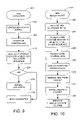
- FIG. 9 provides a flow chart for an MDA ACTIVIATION routine 220 , generally illustrative of preferred steps carried out in accordance with the foregoing discussion to apply input power to storage devices 100 in an MDA.
- An MDA power supply such as 164 is first preferably enabled at step 222 . This may be carried out, for example, by the provision of input power from an upstream source such as on paths 156 and 158 .
- One or more controllers such as 152 , 154 of the MDA are next powered up at step 224 . This is preferably carried out via the MDA power supply 164 and the secondary distribution module 166 . Preferably, remaining steps of the routine 220 are carried out under the direction of the initialized controllers.
- a plurality of storage devices in the MDA are powered up in a selected time-staggered (ordered) sequence. As discussed above, this is preferably carried out by the power management block 184 which sequentially activates the respective switching devices 190 one after another. As desired, input profiling is provided to the switching devices via profile generators 188 . Moreover, as desired different profiles are used for different ones of the nominally identical devices 100 during the staggered power-up sequence.
- Step 228 inquires as to whether the storage devices 100 have been successfully initialized; if so, the MDA proceeds with normal operation at step 230 . If not, diagnostic routines may be run such as represented at step 232 to address the situation and implement appropriate corrective actions.
- An MDA REPLACEMENT routine 240 is set forth by FIG. 10 , generally representative of steps carried out to remove and replace a selected MDA from the system.
- an MDA shutdown signal is first provided. This signal is contemplated as being generated in response to some higher order routine which has identified and initiated the MDA replacement operation.
- the storage devices are powered down in a selected time-order sequence at step 244 . This is preferably carried out by the control block 186 as discussed above.
- the profile generators 188 can be advantageously used to further control the disconnection of each of the input power paths to the system 140 .
- step 246 the routine continues to step 246 wherein the controllers are similarly powered down.
- the preferred embodiments presented above do not specifically utilize the power management 184 to control the activation state of the controllers 124 , 126 , it will be appreciated that such circuitry can also be used to activate the controllers as desired.
- An optional deactivated status signal can be generated and transmitted at step 248 to confirm that the MDA 152 has been successfully powered down. This can be carried out in a number of ways, including through an attempt by the host server 128 to communicate with the deactivated MDA.
- the MDA is removed from the cabinet at step 250 .
- this includes physical manipulation of the MDA to disconnect it from the primary distribution module 150 and to slide it out of the cabinet or associated housing.
- a replacement MDA is next installed onto the primary distribution module 150 at step 252 , and the MDA ACTIVATION routine 220 of FIG. 9 is performed upon the new replacement MDA.
- the assembly may be of substantial weight (e.g., 30-40 pounds or more). Since the MDA incorporates a significant number of rotating masses during operation (e.g., spindle motors, media, etc.), attempting to physically remove an MDA while the MDA is in a fully operational state can result in unexpected and undesired rotational forces.
- the routine of FIG. 10 advantageously reduces a likelihood of damage to the MDA or injury to personnel by controllably placing the MDA in a deactivated state prior to removal.
- the circuit 184 is configured to selectively alter the input power state of a single, individual device 100 in the MDA.
- Spare devices 100 within the array, or devices that are not necessary to implement a particular RAID configuration based on current usage requirements, can fall within this category.
- individual devices 100 may also be identified for replacement such as for routine maintenance efforts or because of abnormal operational characteristics (disc failures, over temperature conditions, etc.).
- FIG. 11 thus sets forth an INDIVIDUAL DEVICE POWER STATE ALTERATION routine 260 , representative of preferred steps carried out in accordance with preferred embodiments to alter the power state of a particular device (e.g., power up from a deactivated state, power down from an activated state).
- INDIVIDUAL DEVICE POWER STATE ALTERATION routine 260 representative of preferred steps carried out in accordance with preferred embodiments to alter the power state of a particular device (e.g., power up from a deactivated state, power down from an activated state).
- a selected storage device 100 is identified for which the input power state is to be altered. As indicated above, this can result from operational loading requirements of the system, the detection of a failure condition for the device, etc. This information is preferably communicated to the control block 186 .
- the input power to the selected device is altered from a first state to a second state in accordance with a selected time-varying profile.
- This is preferably carried out by the profile generator 188 in conjunction with the switching device 190 for each power level associated with the device 100 (e.g., +5 VDC and +12 VDC, respectively). This serves to either power up or power down the selected device, depending on the requirements of step 262 .
- the routine continues to step 266 where a replacement of the MDA 152 can be scheduled.
- the routine then proceeds to carry out the MDA REPLACEMENT routine 240 of FIG. 10 , with an additional step of replacing the failed device 100 in the MDA prior to replacement.
Abstract
Description
Claims (20)
Priority Applications (1)
| Application Number | Priority Date | Filing Date | Title |
|---|---|---|---|
| US11/479,364 US7661005B2 (en) | 2006-06-30 | 2006-06-30 | Individual storage device power control in a multi-device array |
Applications Claiming Priority (1)
| Application Number | Priority Date | Filing Date | Title |
|---|---|---|---|
| US11/479,364 US7661005B2 (en) | 2006-06-30 | 2006-06-30 | Individual storage device power control in a multi-device array |
Publications (2)
| Publication Number | Publication Date |
|---|---|
| US20080005595A1 US20080005595A1 (en) | 2008-01-03 |
| US7661005B2 true US7661005B2 (en) | 2010-02-09 |
Family
ID=38878302
Family Applications (1)
| Application Number | Title | Priority Date | Filing Date |
|---|---|---|---|
| US11/479,364 Expired - Fee Related US7661005B2 (en) | 2006-06-30 | 2006-06-30 | Individual storage device power control in a multi-device array |
Country Status (1)
| Country | Link |
|---|---|
| US (1) | US7661005B2 (en) |
Cited By (8)
| Publication number | Priority date | Publication date | Assignee | Title |
|---|---|---|---|---|
| WO1995022254A1 (en) * | 1994-02-17 | 1995-08-24 | Merck Patent Gmbh | Antiviral or antifungal composition and method |
| US20080229131A1 (en) * | 2007-03-12 | 2008-09-18 | Yasutaka Kono | Storage System and Management Information Acquisition Method for Power Saving |
| US8943274B2 (en) | 2012-05-22 | 2015-01-27 | Seagate Technology Llc | Changing power state with an elastic cache |
| US9058835B2 (en) | 2013-03-13 | 2015-06-16 | Western Digital Technologies, Inc. | Methods and systems for optimized staggered disk drive spinup |
| US20150331465A1 (en) * | 2014-05-13 | 2015-11-19 | Netapp, Inc. | Cascading startup power draws of enclosures across a network |
| US20150362983A1 (en) * | 2014-06-13 | 2015-12-17 | Seagate Technology Llc | Selective storage resource powering for data transfer management |
| US9535472B1 (en) * | 2012-03-31 | 2017-01-03 | Western Digital Technologies, Inc. | Redundant power backplane for NAS storage device |
| US11204633B2 (en) * | 2017-05-10 | 2021-12-21 | Zhengzhou Yunhai Information Technology Co., Ltd. | Method for protecting operation of server backboard |
Families Citing this family (10)
| Publication number | Priority date | Publication date | Assignee | Title |
|---|---|---|---|---|
| WO2010068215A1 (en) * | 2008-12-11 | 2010-06-17 | Lsi Corporation | Independent drive power control |
| JP4816983B2 (en) * | 2008-12-26 | 2011-11-16 | 日本電気株式会社 | Disk array device, power control method and power control program for disk array device |
| US8575984B1 (en) | 2010-11-12 | 2013-11-05 | Applied Micro Circuits Corporation | Multistage latch-based isolation cell |
| US9116679B2 (en) * | 2013-03-14 | 2015-08-25 | Western Digital Technologies, Inc. | Storage device powered by a communications interface |
| KR20150047785A (en) * | 2013-10-25 | 2015-05-06 | 삼성전자주식회사 | Server system and storage system |
| US8935567B1 (en) * | 2014-04-30 | 2015-01-13 | Igneous Systems, Inc. | Network addressable storage controller with storage drive profile comparison |
| USRE48835E1 (en) | 2014-04-30 | 2021-11-30 | Rubrik, Inc. | Network addressable storage controller with storage drive profile comparison |
| WO2016108602A1 (en) * | 2014-12-29 | 2016-07-07 | 주식회사 쏠리드 | Node unit of distributed antenna system |
| US9361046B1 (en) | 2015-05-11 | 2016-06-07 | Igneous Systems, Inc. | Wireless data storage chassis |
| US10013172B2 (en) * | 2015-07-10 | 2018-07-03 | The Keyw Corporatin | Electronic data storage device with multiple configurable data storage mediums |
Citations (10)
| Publication number | Priority date | Publication date | Assignee | Title |
|---|---|---|---|---|
| US5587685A (en) | 1994-10-31 | 1996-12-24 | Hewlett-Packard Company | System for suppressing power transients when connecting a disk drive in an operating raid system |
| US5666538A (en) | 1995-06-07 | 1997-09-09 | Ast Research, Inc. | Disk power manager for network servers |
| US20020188711A1 (en) | 2001-02-13 | 2002-12-12 | Confluence Networks, Inc. | Failover processing in a storage system |
| US20030031187A1 (en) | 2001-08-10 | 2003-02-13 | Peter Heffernan | External storage for modular computer systems |
| US6625690B2 (en) * | 1990-07-13 | 2003-09-23 | Hitachi, Ltd. | Disk system and power-on sequence for the same |
| US6868501B2 (en) * | 2000-08-30 | 2005-03-15 | Nec Corporation | System and method for controlling system power by sequentially controlling the initiating of a plurality of disk drive groups |
| US7035972B2 (en) | 2002-09-03 | 2006-04-25 | Copan Systems, Inc. | Method and apparatus for power-efficient high-capacity scalable storage system |
| US20070226523A1 (en) * | 2006-03-23 | 2007-09-27 | Inventec Corporation | System for controlling sequential startup of hard disks |
| US7305572B1 (en) * | 2004-09-27 | 2007-12-04 | Emc Corporation | Disk drive input sequencing for staggered drive spin-up |
| US7370220B1 (en) * | 2003-12-26 | 2008-05-06 | Storage Technology Corporation | Method and apparatus for controlling power sequencing of a plurality of electrical/electronic devices |
-
2006
- 2006-06-30 US US11/479,364 patent/US7661005B2/en not_active Expired - Fee Related
Patent Citations (11)
| Publication number | Priority date | Publication date | Assignee | Title |
|---|---|---|---|---|
| US6625690B2 (en) * | 1990-07-13 | 2003-09-23 | Hitachi, Ltd. | Disk system and power-on sequence for the same |
| US5587685A (en) | 1994-10-31 | 1996-12-24 | Hewlett-Packard Company | System for suppressing power transients when connecting a disk drive in an operating raid system |
| US5666538A (en) | 1995-06-07 | 1997-09-09 | Ast Research, Inc. | Disk power manager for network servers |
| US5961613A (en) | 1995-06-07 | 1999-10-05 | Ast Research, Inc. | Disk power manager for network servers |
| US6868501B2 (en) * | 2000-08-30 | 2005-03-15 | Nec Corporation | System and method for controlling system power by sequentially controlling the initiating of a plurality of disk drive groups |
| US20020188711A1 (en) | 2001-02-13 | 2002-12-12 | Confluence Networks, Inc. | Failover processing in a storage system |
| US20030031187A1 (en) | 2001-08-10 | 2003-02-13 | Peter Heffernan | External storage for modular computer systems |
| US7035972B2 (en) | 2002-09-03 | 2006-04-25 | Copan Systems, Inc. | Method and apparatus for power-efficient high-capacity scalable storage system |
| US7370220B1 (en) * | 2003-12-26 | 2008-05-06 | Storage Technology Corporation | Method and apparatus for controlling power sequencing of a plurality of electrical/electronic devices |
| US7305572B1 (en) * | 2004-09-27 | 2007-12-04 | Emc Corporation | Disk drive input sequencing for staggered drive spin-up |
| US20070226523A1 (en) * | 2006-03-23 | 2007-09-27 | Inventec Corporation | System for controlling sequential startup of hard disks |
Cited By (16)
| Publication number | Priority date | Publication date | Assignee | Title |
|---|---|---|---|---|
| US6187316B1 (en) | 1994-02-17 | 2001-02-13 | Merck Patent Gmbh | Antiviral or antifungal composition and method |
| WO1995022254A1 (en) * | 1994-02-17 | 1995-08-24 | Merck Patent Gmbh | Antiviral or antifungal composition and method |
| US20080229131A1 (en) * | 2007-03-12 | 2008-09-18 | Yasutaka Kono | Storage System and Management Information Acquisition Method for Power Saving |
| US8145930B2 (en) * | 2007-03-12 | 2012-03-27 | Hitachi, Ltd. | Storage system and management information acquisition method for power saving |
| US9535472B1 (en) * | 2012-03-31 | 2017-01-03 | Western Digital Technologies, Inc. | Redundant power backplane for NAS storage device |
| US8943274B2 (en) | 2012-05-22 | 2015-01-27 | Seagate Technology Llc | Changing power state with an elastic cache |
| US9058835B2 (en) | 2013-03-13 | 2015-06-16 | Western Digital Technologies, Inc. | Methods and systems for optimized staggered disk drive spinup |
| US20150331465A1 (en) * | 2014-05-13 | 2015-11-19 | Netapp, Inc. | Cascading startup power draws of enclosures across a network |
| US9766677B2 (en) * | 2014-05-13 | 2017-09-19 | Netapp, Inc. | Cascading startup power draws of enclosures across a network |
| US20150362972A1 (en) * | 2014-06-13 | 2015-12-17 | Seagate Technology Llc | Power characteristics in a system of disparate storage drives |
| US9541978B2 (en) | 2014-06-13 | 2017-01-10 | Seagate Technology Llc | Redundancies for reconstruction in mass data storage systems |
| US20150362983A1 (en) * | 2014-06-13 | 2015-12-17 | Seagate Technology Llc | Selective storage resource powering for data transfer management |
| US9874915B2 (en) | 2014-06-13 | 2018-01-23 | Seagate Technology Llc | Extended file attributes for redundant data storage |
| US9880602B2 (en) * | 2014-06-13 | 2018-01-30 | Seagate Technology Llc | Power characteristics in a system of disparate storage drives |
| US9939865B2 (en) * | 2014-06-13 | 2018-04-10 | Seagate Technology Llc | Selective storage resource powering for data transfer management |
| US11204633B2 (en) * | 2017-05-10 | 2021-12-21 | Zhengzhou Yunhai Information Technology Co., Ltd. | Method for protecting operation of server backboard |
Also Published As
| Publication number | Publication date |
|---|---|
| US20080005595A1 (en) | 2008-01-03 |
Similar Documents
| Publication | Publication Date | Title |
|---|---|---|
| US7661005B2 (en) | Individual storage device power control in a multi-device array | |
| US10503420B2 (en) | Distributed object storage system comprising low power storage nodes | |
| US7423354B2 (en) | Storage system | |
| US8024602B2 (en) | Multipath redundant storage system architecture and method | |
| US8154258B2 (en) | Backup energy storage module with voltage leveling | |
| US20080005469A1 (en) | Temperature control to reduce cascade failures in a multi-device array | |
| US7058826B2 (en) | System, architecture, and method for logical server and other network devices in a dynamically configurable multi-server network environment | |
| US7134011B2 (en) | Apparatus, architecture, and method for integrated modular server system providing dynamically power-managed and work-load managed network devices | |
| US7484111B2 (en) | Power on demand and workload management system and method | |
| US6966006B2 (en) | Adaptive startup policy for accelerating multi-disk array spin-up | |
| US20090144568A1 (en) | Apparatus and method for modular dynamically power managed power supply and cooling system for computer systems, server applications, and other electronic devices | |
| US20060179209A1 (en) | Storage device method and apparatus | |
| US7761659B2 (en) | Wave flushing of cached writeback data to a storage array | |
| CN107291201A (en) | A kind of server power panel | |
| US7878861B2 (en) | Energy storage module including a connector having unique pin configuration | |
| US7404092B2 (en) | Power supply control in a server system | |
| US6954819B2 (en) | Peripheral bus switch to maintain continuous peripheral bus interconnect system operation | |
| JP2005539303A (en) | Method and apparatus for power efficient high capacity scalable storage system | |
| US6126451A (en) | SCSI connector | |
| US8225159B1 (en) | Method and system for implementing power savings features on storage devices within a storage subsystem | |
| JP2001186655A (en) | Method and apparatus for controlling power supply | |
| KR200273395Y1 (en) | A Centralized RAID-PC Network System | |
| KR20030066838A (en) | A Centralized RAID-PC Network System | |
| GB2414307A (en) | Power supply for a storage system |
Legal Events
| Date | Code | Title | Description |
|---|---|---|---|
| AS | Assignment |
Owner name: SEAGATE TECHNOLOGY LLC,CALIFORNIA Free format text: ASSIGNMENT OF ASSIGNORS INTEREST;ASSIGNORS:SPENGLER, DAVID LOUIS;LAWLOR, THOMAS M.;DECENZO, DAVID P.;AND OTHERS;REEL/FRAME:018071/0778 Effective date: 20060629 Owner name: SEAGATE TECHNOLOGY LLC, CALIFORNIA Free format text: ASSIGNMENT OF ASSIGNORS INTEREST;ASSIGNORS:SPENGLER, DAVID LOUIS;LAWLOR, THOMAS M.;DECENZO, DAVID P.;AND OTHERS;REEL/FRAME:018071/0778 Effective date: 20060629 |
|
| AS | Assignment |
Owner name: WELLS FARGO BANK, NATIONAL ASSOCIATION, AS COLLATE Free format text: SECURITY AGREEMENT;ASSIGNORS:MAXTOR CORPORATION;SEAGATE TECHNOLOGY LLC;SEAGATE TECHNOLOGY INTERNATIONAL;REEL/FRAME:022757/0017 Effective date: 20090507 Owner name: JPMORGAN CHASE BANK, N.A., AS ADMINISTRATIVE AGENT Free format text: SECURITY AGREEMENT;ASSIGNORS:MAXTOR CORPORATION;SEAGATE TECHNOLOGY LLC;SEAGATE TECHNOLOGY INTERNATIONAL;REEL/FRAME:022757/0017 Effective date: 20090507 |
|
| STCF | Information on status: patent grant |
Free format text: PATENTED CASE |
|
| CC | Certificate of correction | ||
| FEPP | Fee payment procedure |
Free format text: PAYOR NUMBER ASSIGNED (ORIGINAL EVENT CODE: ASPN); ENTITY STATUS OF PATENT OWNER: LARGE ENTITY |
|
| AS | Assignment |
Owner name: SEAGATE TECHNOLOGY INTERNATIONAL, CALIFORNIA Free format text: RELEASE;ASSIGNOR:JPMORGAN CHASE BANK, N.A., AS ADMINISTRATIVE AGENT;REEL/FRAME:025662/0001 Effective date: 20110114 Owner name: SEAGATE TECHNOLOGY LLC, CALIFORNIA Free format text: RELEASE;ASSIGNOR:JPMORGAN CHASE BANK, N.A., AS ADMINISTRATIVE AGENT;REEL/FRAME:025662/0001 Effective date: 20110114 Owner name: MAXTOR CORPORATION, CALIFORNIA Free format text: RELEASE;ASSIGNOR:JPMORGAN CHASE BANK, N.A., AS ADMINISTRATIVE AGENT;REEL/FRAME:025662/0001 Effective date: 20110114 Owner name: SEAGATE TECHNOLOGY HDD HOLDINGS, CALIFORNIA Free format text: RELEASE;ASSIGNOR:JPMORGAN CHASE BANK, N.A., AS ADMINISTRATIVE AGENT;REEL/FRAME:025662/0001 Effective date: 20110114 |
|
| AS | Assignment |
Owner name: THE BANK OF NOVA SCOTIA, AS ADMINISTRATIVE AGENT, Free format text: SECURITY AGREEMENT;ASSIGNOR:SEAGATE TECHNOLOGY LLC;REEL/FRAME:026010/0350 Effective date: 20110118 |
|
| FPAY | Fee payment |
Year of fee payment: 4 |
|
| AS | Assignment |
Owner name: SEAGATE TECHNOLOGY US HOLDINGS, INC., CALIFORNIA Free format text: TERMINATION AND RELEASE OF SECURITY INTEREST IN PATENT RIGHTS;ASSIGNOR:WELLS FARGO BANK, NATIONAL ASSOCIATION, AS COLLATERAL AGENT AND SECOND PRIORITY REPRESENTATIVE;REEL/FRAME:030833/0001 Effective date: 20130312 Owner name: EVAULT INC. (F/K/A I365 INC.), CALIFORNIA Free format text: TERMINATION AND RELEASE OF SECURITY INTEREST IN PATENT RIGHTS;ASSIGNOR:WELLS FARGO BANK, NATIONAL ASSOCIATION, AS COLLATERAL AGENT AND SECOND PRIORITY REPRESENTATIVE;REEL/FRAME:030833/0001 Effective date: 20130312 Owner name: SEAGATE TECHNOLOGY INTERNATIONAL, CAYMAN ISLANDS Free format text: TERMINATION AND RELEASE OF SECURITY INTEREST IN PATENT RIGHTS;ASSIGNOR:WELLS FARGO BANK, NATIONAL ASSOCIATION, AS COLLATERAL AGENT AND SECOND PRIORITY REPRESENTATIVE;REEL/FRAME:030833/0001 Effective date: 20130312 Owner name: SEAGATE TECHNOLOGY LLC, CALIFORNIA Free format text: TERMINATION AND RELEASE OF SECURITY INTEREST IN PATENT RIGHTS;ASSIGNOR:WELLS FARGO BANK, NATIONAL ASSOCIATION, AS COLLATERAL AGENT AND SECOND PRIORITY REPRESENTATIVE;REEL/FRAME:030833/0001 Effective date: 20130312 |
|
| FPAY | Fee payment |
Year of fee payment: 8 |
|
| SULP | Surcharge for late payment |
Year of fee payment: 7 |
|
| FEPP | Fee payment procedure |
Free format text: MAINTENANCE FEE REMINDER MAILED (ORIGINAL EVENT CODE: REM.); ENTITY STATUS OF PATENT OWNER: LARGE ENTITY |
|
| LAPS | Lapse for failure to pay maintenance fees |
Free format text: PATENT EXPIRED FOR FAILURE TO PAY MAINTENANCE FEES (ORIGINAL EVENT CODE: EXP.); ENTITY STATUS OF PATENT OWNER: LARGE ENTITY |
|
| STCH | Information on status: patent discontinuation |
Free format text: PATENT EXPIRED DUE TO NONPAYMENT OF MAINTENANCE FEES UNDER 37 CFR 1.362 |
|
| FP | Lapsed due to failure to pay maintenance fee |
Effective date: 20220209 |