US7673520B2 - Device and method for testing electronic components - Google Patents
Device and method for testing electronic components Download PDFInfo
- Publication number
- US7673520B2 US7673520B2 US11/683,279 US68327907A US7673520B2 US 7673520 B2 US7673520 B2 US 7673520B2 US 68327907 A US68327907 A US 68327907A US 7673520 B2 US7673520 B2 US 7673520B2
- Authority
- US
- United States
- Prior art keywords
- loading
- transfer element
- transfer
- test position
- single test
- Prior art date
- Legal status (The legal status is an assumption and is not a legal conclusion. Google has not performed a legal analysis and makes no representation as to the accuracy of the status listed.)
- Expired - Fee Related, expires
Links
Images


Classifications
-
- G—PHYSICS
- G01—MEASURING; TESTING
- G01R—MEASURING ELECTRIC VARIABLES; MEASURING MAGNETIC VARIABLES
- G01R31/00—Arrangements for testing electric properties; Arrangements for locating electric faults; Arrangements for electrical testing characterised by what is being tested not provided for elsewhere
- G01R31/28—Testing of electronic circuits, e.g. by signal tracer
- G01R31/2851—Testing of integrated circuits [IC]
- G01R31/2893—Handling, conveying or loading, e.g. belts, boats, vacuum fingers
Definitions
- Electronic components are normally tested for their electronic or electrical characteristics after production. This can be carried out both at ambient temperature as well as at increased or reduced temperature.
- index time This is the time needed to exchange a tested component for one that is still to be tested.
- the object of the invention is to reduce the index time.
- the device comprises two loading positions and a common test position.
- transfer elements an electronic component can be passed from in each case one or two loading positions to the common test position. While one electronic component is being tested, the other transfer element can output a tested component and accept a component to be tested.
- the index time is thus only determined by the time which is needed to exchange the two transfer elements in the test position.
- the time which is needed to output an electronic component from a transfer element and to load it with a new electronic component which is to be tested is then no longer relevant. This applies at least provided the electrical testing time is longer than the time needed to remove an electronic component from a transfer element and to pass a component to be tested to it.
- the path which a transfer element can take between the loading position and the test position can be designed in many different ways. It can, for example, be in a straight line, curve-shaped, S-shaped or also be composed of straight-line, curve-shaped or S-shaped sections.
- the orientation of the transfer element in the loading position and in the test position can be the same. This means that the transfer element could be transferred from the loading to the test position with a pure translational movement without it being superimposed with a rotational movement of the transfer element.
- the transfer elements take on various orientations in the loading and test positions. This facilitates other driving methods and other configurations which lead to a more compact embodiment.
- the paths between the two loading positions and the common test position run congruently to at least directly in front of the test position. This facilitates the arrangement of the two paths such that the electrical contacts of the electrical testing head are worn as little as possible, because a laterally aligned motional component on contacting the electrical contacts of the electrical testing head is avoided. A perpendicular meeting of the contacts is advantageous for low contact wear.
- the paths for the transfer elements can be realised in various ways.
- guides such as rods, rails, grooves, cranks or similar devices are possible. This type of embodiment facilitates a permanently defined path guide which has a low susceptibility to wear.
- One embodiment in which the two transfer elements are connected to a common driving means is particularly advantageous. Consequently, it is possible to provide just one driving means for both transfer elements, which leads to an inexpensive embodiment.
- the two transfer elements can be joined by mechanically rigid joining elements, such as rods, shaped elements or similar devices to the common driving means. This facilitates devices which are as simple and as reliable as possible.
- a common driving means which is particularly advantageous is a rotating element, such as a rotary table or a rotating cylinder or also a rotating rod which can be driven pneumatically, electrically, hydraulically or by a stepper motor or servomotor.
- This type of driving means with a rotating element comprises in each case parts of a rotating element with opposed directions of motion, which can be used for the opposed movements of two transfer elements.
- the electronic components can be passed to both loading positions independently via two separate channels. It is however also possible to provide an at least partially common channel, which is separated into two subchannels just in front of the respective loading positions. With the failure of a loading position or a transfer element the other can then continue to be operated even if with less total capacity. This is particularly advantageous if, for example, only a few components are still to be tested.
- one or other or both transfer elements are coupled in each case to a further transfer element.
- two transfer elements can be provided one above the other which are coupled together such that they preferably can move simultaneously. If both transfer elements comprise a further transfer element in each case, then a total of four transfer elements are provided.
- two can be arranged one above the other and in each case one adjacent to the other.
- the two transfer elements which are positioned one above the other are coupled together for simultaneous movement, whereas the adjacent elements are provided for alternating movement.
- the device is preferably a gravity handler.
- a gravity handler the electronic components to be tested are moved by the force of gravity. In this respect they are moved along a transport path by the force of gravity.
- the electronic components can, for example, drop into the transfer elements by the effect of the force of gravity and/or drop out of them by the effect of the force of gravity.
- the path which the electronic components take for testing is essentially arranged vertically, but can also be slightly tilted in certain regions.
- the counterpart to gravity handlers are the so-called pick-and-place handlers in which the electronic components are moved essentially horizontally by appropriate devices and not by the force of gravity and are on the contrary moved in a controlled manner by appropriate devices.
- Another device for the testing of electronic components comprises two mechanical transfer elements which however exhibit a common loading position and a common test position.
- a tested component While one electronic component is being tested, a tested component is removed from the other transfer element and it is loaded with an electronic component to be tested. This can take place simultaneously with the testing of another electronic component so that time is gained.
- each transfer element in the common loading position and in the common test position has in each case the same orientation.
- the avoidance of rotary movements of the transfer elements leads to an improved positional accuracy of the electronic components in the respective transfer element.
- the two transfer elements are driven by a common drive element, wherein it is designed such that with only one drive element causing a movement of the transfer elements, the movement from the loading position into the test position can be achieved.
- This facilitates fast interchange of the two transfer elements. If several drive elements have to be used for different sections of the movement, this increases the time requirement, because the two movements must be executed consecutively.
- an embodiment with two or three or more driving means is not excluded.
- this device is preferably a gravity handler.
- the loading of the transfer elements occurs respectively by a movement of electronic components which is caused by the force of gravity. Otherwise, for example, the same applies as for the gravity handler described above.
- a first transfer element is loaded with a first (still to be tested) electronic component in a first loading position and at least partly simultaneously a second electronic component is tested in a second transfer element in a test position. After conclusion of the test, the second transfer element is moved out of the test position and then or at least partially simultaneously the first transfer element is passed to the common test position.
- a first transfer element is loaded with a first (still to be tested) electronic component in a common loading position and at least simultaneously an electronic component of a second transfer element is tested in a test position.
- the second transfer element is in this case located in the test position. Thereafter, the second transfer element is moved away from the common test position and then or at least partially simultaneously the first transfer element is passed to the test position.
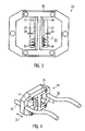
- FIG. 1 a schematic view of a device for the testing of electronic components
- FIG. 2 various possible configurations for transfer elements in the loading and test positions
- FIG. 3 a detail view of a transfer element
- FIG. 4 a three-dimensional schematic view of a transfer element with guides
- FIG. 5 possible embodiments of the drive and the guide of transfer elements
- FIG. 6 a schematic view of feed and removal channels together with transfer elements
- FIG. 7 a schematic view of a number of transfer elements arranged adjacently and one above the other;
- FIG. 8 an alternative embodiment with a common loading position
- FIG. 9 various states during a run through the process.
- FIG. 1 shows a schematic view of a device 1 for the testing of electronic components 3 .
- the electronic components 3 such as typically IC chips or similar components, can be heated or cooled in a temperature stabilising device 2 to a predetermined temperature.
- the temperature stabilising device 2 does not however need to be used or provided. Testing the components at room temperature is also possible.
- the device is a gravity handler.
- the path taken by the electronic components is essentially vertical.
- the electronic components 3 are singled out and passed along a guide channel 4 to a transfer element 5 .
- a suitable singling out device can be provided and one or more stoppers to specifically stop the various electronic components along the channel.
- the movements of the electronic components are caused, at least in part, by the force of gravity.
- An electronic component 3 is introduced into the transfer element 5 (e.g. by dropping into it), as illustrated in FIG. 1 .
- the transfer element 5 can then be brought along the guide 6 into the test position 7 .
- Adjacent to the test position 7 there is an electrical testing head 8 , which is controlled by a test device 9 which is illustrated schematically. With the electrical testing head 8 , the electrical terminals of an electronic component 3 can be contacted in order to test it in relation to its electronic characteristics.
- the transfer element 5 is moved back from the test position 7 into the loading position (refer to FIG. 1 ) in order to output the tested electronic component 3 downwards (e.g. by dropping down due to the force of gravity) and a new electronic component still to be tested is accepted from above.
- FIG. 1 only one transfer element 5 can be seen in the illustration, because a second transfer element is covered by the first transfer element.
- various branches can be provided to guide the tested electronic components 3 into one or other ejection channel or reservoir 11 , 12 , 13 , depending on the test result.
- FIG. 2 illustrates sectional views at the height of the transfer element 5 shown in plan view in FIG. 1 .
- the illustrations are schematic and show essentially the respective loading positions of a transfer element 5 a , 5 b and the test position 7 .
- FIG. 2 a a first transfer element 5 a and a second transfer element 5 b are arranged adjacently.
- Each of these two transfer elements can be loaded with electronic components 3 (from above, i.e. from a direction above the drawing plane) and each of these transfer elements can output tested electronic components downwards (in a direction below the drawing plane).
- the two transfer elements 5 a , 5 b can each be transferred individually into the common test position 7 along the paths 14 a , 14 b .
- the return occurs in each case along the same path. However, other paths are also possible for the return.
- FIG. 2 a an intermediate position with the reference number 15 is indicated.
- the transfer element 5 a in the position 15 exhibits the same orientation as in the loading position or as in the test position 7 . From the loading position the transfer element 5 a can be transferred with a purely linear displacement into the position 15 or the position 7 without a rotational movement being superimposed. This means that the orientation is in each case the same.
- FIG. 2 b shows that the intermediate position 15 ′ can also be rotated relative to the loading or test position 7 .
- an embodiment of this nature is advantageous in which the orientation of the transfer element 5 a , 5 b does not, or does not significantly change in comparison to the tangent of the path 14 a , 14 b on which the transfer element 5 a , 5 b is currently located. This simplifies the guidance along defined guides. The loading and the test position 7 however exhibits the same orientation even when in FIG. 2 b the intermediate position is rotated.
- the paths 14 a , 14 b are formed from two curve-shaped pieces with opposing curve directions. Thus, essentially S-shaped curves are formed.
- the transfer elements 5 a , 5 b can be guided into the test position 7 , but also along straight-line paths 16 a , 16 b .
- a corresponding intermediate position is illustrated under reference number 17 .
- FIG. 2 d furthermore illustrates that directly in front of the test position 7 a path section 19 can be provided, along which the paths 18 a , 18 b , which are only outlined here in dashes schematically, lie congruently one above the other.
- This facilitates the vertical running in of the transfer elements 5 a , 5 b onto the electrical testing head 8 . Consequently, wear of the electrical contacts of the electrical testing head 8 is reduced, because no grinding lateral movements occur, as could occur for example in FIG. 2 c.
- the paths 18 a and 18 b in FIG. 2 d can be formed in a straight line or curved, formed in an S-shape or any other shape.
- FIG. 2 e the two loading positions of transfer elements 20 a , 20 b are not adjacent, but rather arranged opposite one another.
- the positions illustrated in FIG. 2 e arise through 90° rotation of the positions in FIGS. 2 a - 2 d .
- larger or smaller angles of rotation than 90° are conceivable, such as for example 30°, 45°, 60° or more or less than 30°, 45°, or 60°.
- a transfer element 20 a , 20 b can be brought into the test position 7 by a swivel movement. Furthermore, vertical introduction into the test position 7 is also ensured here.
- the transfer element 20 a can be transferred into the position 7 about a swivelling axle 22 a . This is a pure rotational movement without a linear component. The same applies to the transfer element 20 b when swivelled about the axle 22 b .
- the respective paths are labelled with 21 a , 21 b.
- FIG. 2 f a further possible embodiment is shown in which the loading position of the transfer elements 23 a and 23 b are located diagonally in relation to the positions in FIGS. 2 a - 2 d and 2 e . From a position of this nature the transfer of the transfer elements 23 a , 23 b into the test position 7 can be achieved with a purely rotational movement or, as illustrated in FIG. 2 f , with a movement which is composed of a straight, a curved and a straight movement. The required angles of rotation are smaller in comparison to FIG. 2 e so that the movement can be executed faster.
- FIG. 3 A detail view of a transfer element is illustrated in FIG. 3 . It bears the reference number 24 and corresponds to the transfer elements 5 a , 5 b , 20 a , 20 b , 23 a , 23 b in FIG. 2 .
- FIG. 4 a three-dimensional schematic view of the transfer element 24 from FIG. 3 is schematically illustrated.
- the transfer element 24 exhibits a frame around one or two openings 29 on which a double T-shaped element 25 with a bridge 31 is attached.
- An electronic component to be tested can slide downwards from above between the base of the transfer element 24 and the bridge 31 .
- a stopper 27 is provided, which can engage the electrical contacts 30 of an electronic component 3 to be tested with appropriate projections (refer to the lower end of the stopper 27 ).
- Other stoppers which engage the body of the electronic component to be tested, are additionally or alternatively possible. Vacuum apertures, which firmly suck onto an electronic component, can also be provided as stoppers.
- the electronic component 3 can be released by a movement of the stoppers 27 outwards (direction 28 ) so that it can slide out downwards.
- an insulator material 26 is arranged which provides insulation for the electrical contacts 30 of the electronic component 3 against the bridge 31 and guides the electronic component.
- the electronic contacts are accessible externally and can be contacted by the contacts of the electrical testing head 8 .
- FIG. 4 a guide of rods 32 is additionally shown as an example.
- the transfer element 24 can be moved forwards and backwards in the direction 33 along these rods 32 .
- an S-shaped guide for the transfer element 24 is thus possible.
- FIG. 5 a a preferred variant for the drive of the transfer elements is illustrated.
- the transfer elements have the reference numbers 43 a and 43 b.
- a plate 40 with grooves 41 and 42 is provided below the transfer elements. For a better graphical illustration this plate 40 is shown here below along the dashed line, offset as in an exploded drawing.
- Shuttles 44 a , 44 b can slide in the grooves 41 and 42 . These shuttles 44 a , 44 b can be arranged partially in front of or behind the respective transfer element 43 a , 43 b or also on both sides of it.
- the shuttles are advantageously at least so long that they are longer than the common path section of the grooves 41 , 42 on the common path section positioned at the front left in FIG. 5 a . This ensures that a shuttle 44 b entering the groove 41 is also guided back again into this groove. This applies correspondingly to shuttle 44 a.
- two separate path guides can also be provided. This is, for example, possible in that the shuttles are not located centrally at the transfer elements, but rather are in each case offset to the outside. This is also advantageous for an output of the tested electronic components, because otherwise a shuttle could be in the way.
- a holder 45 a or 45 b is arranged together with a rod 46 a , 46 b on the transfer elements 43 a , 43 b .
- the rods 46 a , 46 b are connected via rotational points 49 a , 49 b to a rotatable disc 47 .
- the disc 47 can essentially be rotated to and fro, wherein this occurs about an axle 48 using a motor 49 .
- the motor 49 can be a pneumatic motor actuator, a stepper motor, a servomotor or another type of motor.
- connection between the rotatable disc 47 and the transfer elements 43 a , 43 b can also be realised via the shuttles 44 a , 44 b in that the rods 46 or the holders 45 engage the shuttles.
- FIG. 5 b Another form of drive is illustrated in FIG. 5 b .
- an xy (dual-axis) drive is in each case provided for both of the transfer elements 50 a , 50 b which can be moved along the paths 51 a and 51 b .
- a motor actuator 52 b can move another motor actuator 53 b to and fro in the direction 55 .
- the motor actuator 53 b can move a beam 54 b to and fro in a direction 56 .
- the transfer elements 63 a and 63 b are illustrated in their respective loading positions and the view is in the direction from the electrical testing head onto the device of FIG. 1 .
- the test position 64 is illustrated dashed in the direction in front of the drawing plane.
- Feed channels 62 a , 62 b for the two loading positions are illustrated above the loading position. These can be in a straight line and/or independent of one another. In FIG. 6 an embodiment is however illustrated in which both channels 62 a , 62 b are served from one common channel 60 .
- the switch 61 is schematically illustrated with which electronic components 3 to be tested can be directed from the channel 60 either into channel 62 a or into channel 62 b.
- channels 66 a and 66 b Downstream from the loading positions two channels 66 a and 66 b are provided here, which can also be formed independently of one another. Preferably they lead straight downwards (refer also to FIG. 1 with channel 10 ).
- FIG. 6 however an embodiment is shown in which the two channels 66 a and 66 b open into a common channel 67 .
- This facilitates the use of just one channel with appropriate branches into the containers 11 , 12 , 13 , (refer to FIG. 1 ).
- With two independent channels double the number of branches are needed, which is more complicated mechanically.
- FIG. 7 illustrates a possible arrangement of a number of transfer elements 5 arranged adjacently and one above the other.
- the two left transfer elements 5 in the top row can, for example, be used to serve a common test position, whereas the two right transfer elements in the top row can be used to serve another test position.
- the transfer elements 5 located respectively one above the other are advantageously mechanically coupled together directly or indirectly so that they can be moved together. Consequently, it is possible to serve two electrical test positions located one above the other respectively alternately with the transfer elements 5 of the first and second column (from the left in FIG. 7 ).
- the four transfer elements 5 on the left in FIG. 7 can be driven by a single motor. The same applies correspondingly to the four transfer elements 5 arranged on the right in FIG. 7 .
- the electronic components 3 can be conveyed out of the respective top transfer elements 5 through the lower transfer elements 5 to the output and electronic components to be tested, which are for the respective lower transfer element, are passed through the upper transfer element.
- FIG. 8 Another embodiment is illustrated in FIG. 8 in which a common loading position is provided for two transfer elements 80 a , 80 b .
- Two paths 82 a and 82 b are provided between the loading position 88 and the test position 89 , wherein the transfer element 80 b is to be moved along the path 82 b and the transfer element 80 a along the path 82 a (refer also to FIG. 8 b ).
- the drive is realised similar as shown in FIG. 5 a with a rotating element 87 and two rods 81 a , 81 b , each of which is supported at rotating points 84 a , 84 b .
- the rods engage directly with the transfer elements 80 a , 80 b , as is also possible in FIG. 5 a.
- FIG. 9 A method of operation will now be explained using FIG. 9 as an example.
- FIG. 9 a a transfer element 90 a is illustrated in a loading position 92 a . In this position it can be loaded with an electronic component to be tested.
- the other transfer element 90 b is located in the common test position 91 . Here, it can be tested by the electrical testing head 8 (refer to FIG. 1 ).
- the transfer element 90 b is transferred from the common test position 91 into the loading position 92 b (refer to FIG. 9 b ). In this position the tested electronic component can be output downwards (refer to FIGS. 1 and 6 ) and loaded with a new component to be tested.
- the transfer element 90 b moves out of the common test position 91 into the loading position 92 b or at least partially during this movement or also thereafter, the transfer element 90 a can be transferred out of the loading position 92 a into the common test position 91 .
- the component can then be tested.
- the transfer element 90 a is moved out of the common test position 91 again back into the loading position 92 a (refer to FIG. 9 a ) and in the meantime or thereafter the transfer element 90 b is transferred out of the loading position with the new electronic component to be tested from the loading position 92 b into the common test position 91 (refer to FIG. 9 a ).
- This sequence can be repeated to test many components.
- the method of operation with the device from FIG. 8 is precisely the same except that two separate positions 92 a , 92 b are not provided, but instead there is a common loading position.
Abstract
Description
Claims (21)
Applications Claiming Priority (6)
| Application Number | Priority Date | Filing Date | Title |
|---|---|---|---|
| EP06004765 | 2006-03-08 | ||
| EP06004765.1 | 2006-03-08 | ||
| EP06004765 | 2006-03-08 | ||
| EP06024651.9A EP1832886B1 (en) | 2006-03-08 | 2006-11-28 | Device and method for testing electronic components |
| EP06024651.9 | 2006-11-28 | ||
| EP06024651 | 2006-11-28 |
Publications (2)
| Publication Number | Publication Date |
|---|---|
| US20070212201A1 US20070212201A1 (en) | 2007-09-13 |
| US7673520B2 true US7673520B2 (en) | 2010-03-09 |
Family
ID=38370705
Family Applications (1)
| Application Number | Title | Priority Date | Filing Date |
|---|---|---|---|
| US11/683,279 Expired - Fee Related US7673520B2 (en) | 2006-03-08 | 2007-03-07 | Device and method for testing electronic components |
Country Status (3)
| Country | Link |
|---|---|
| US (1) | US7673520B2 (en) |
| EP (1) | EP1832886B1 (en) |
| MY (1) | MY146701A (en) |
Cited By (1)
| Publication number | Priority date | Publication date | Assignee | Title |
|---|---|---|---|---|
| US20100150686A1 (en) * | 2007-10-05 | 2010-06-17 | Multitest Elektronische Systeme Gmbh | Handler for electronic components, in particular ic's, comprising a pneumatic cylinder displacement unit for moving plungers |
Families Citing this family (2)
| Publication number | Priority date | Publication date | Assignee | Title |
|---|---|---|---|---|
| US9594111B2 (en) * | 2013-02-27 | 2017-03-14 | Infineon Technologies Ag | Turret handlers and methods of operations thereof |
| DE102014107314B3 (en) * | 2014-05-23 | 2015-10-22 | Multitest Elektronische Systeme Gmbh | Guide and support member for a device for testing electronic components |
Citations (20)
| Publication number | Priority date | Publication date | Assignee | Title |
|---|---|---|---|---|
| US4128174A (en) * | 1977-02-28 | 1978-12-05 | Motorola, Inc. | High-speed integrated circuit handler |
| US4506213A (en) | 1983-07-18 | 1985-03-19 | Sym-Tek Systems, Inc. | Electronic device handler |
| US4691831A (en) * | 1984-06-25 | 1987-09-08 | Takeda Riken Co., Ltd. | IC test equipment |
| DE3715671A1 (en) | 1987-05-11 | 1988-11-24 | Ekkehard Ueberreiter | Device for testing and sorting electronic components, particularly chips with integrated circuits (ICs) |
| WO1992004989A1 (en) | 1990-09-24 | 1992-04-02 | Sym-Tek Systems, Inc. | Electronic device test handler |
| US5151651A (en) * | 1990-08-16 | 1992-09-29 | Tokyo Electron Limited | Apparatus for testing IC elements |
| US5184068A (en) * | 1990-09-24 | 1993-02-02 | Symtek Systems, Inc. | Electronic device test handler |
| US5650732A (en) * | 1993-07-02 | 1997-07-22 | Mitsubishi Denki Kabushiki Kaisha | Semiconductor device test system |
| US5801527A (en) | 1994-07-26 | 1998-09-01 | Tokyo Electron Limited | Apparatus and method for testing semiconductor device |
| US5919024A (en) | 1996-07-15 | 1999-07-06 | Seiko Epson Corporation | Parts handling apparatus |
| US6163146A (en) * | 1997-03-18 | 2000-12-19 | Advantest Corporation | IC testing method |
| US6339321B1 (en) * | 1998-05-29 | 2002-01-15 | Advantest Corporation | Electronic device tray electronic device tray, transporting apparatus, and electronic device testing apparatus |
| US6364089B1 (en) * | 1999-12-10 | 2002-04-02 | National Semiconductor Corporation | Multi-station rotary die handling device |
| US6479777B2 (en) * | 1997-11-12 | 2002-11-12 | Murata Manufacturing Co., Inc. | Electronic parts conveying apparatus and method |
| US6518745B2 (en) * | 2000-10-10 | 2003-02-11 | Mirae Corporation | Device test handler and method for operating the same |
| US6579057B2 (en) * | 2000-06-08 | 2003-06-17 | Kabushiki Kaisha Shinkawa | Conveyor apparatus for dies and small components |
| US20040164723A1 (en) | 2003-02-20 | 2004-08-26 | Mirae Corporation | Indexing device in semiconductor device handler and method for operating the same |
| US20050168233A1 (en) * | 2004-01-29 | 2005-08-04 | Howard Roberts | Test system and method for reduced index time |
| US7225531B2 (en) * | 2001-01-09 | 2007-06-05 | Mirae Corporation | Index head in semicondcutor device test handler |
| US7274202B2 (en) * | 2005-10-07 | 2007-09-25 | Verigy (Singapore) Pte. Ltd. | Carousel device, system and method for electronic circuit tester |
Family Cites Families (3)
| Publication number | Priority date | Publication date | Assignee | Title |
|---|---|---|---|---|
| DE3634860A1 (en) * | 1986-10-13 | 1988-04-14 | Microhandling Handhabungsgerae | Device for sorting and simultaneously twisting (intrinsic rotation through 180@) of components in the form of parallelepipeds |
| DE3719148A1 (en) * | 1987-06-09 | 1988-12-29 | Willberg Hans Heinrich | Device for testing and sorting electronic components, particularly ICs |
| US6731127B2 (en) * | 2001-12-21 | 2004-05-04 | Texas Instruments Incorporated | Parallel integrated circuit test apparatus and test method |
-
2006
- 2006-11-28 EP EP06024651.9A patent/EP1832886B1/en not_active Not-in-force
-
2007
- 2007-03-05 MY MYPI20070337A patent/MY146701A/en unknown
- 2007-03-07 US US11/683,279 patent/US7673520B2/en not_active Expired - Fee Related
Patent Citations (22)
| Publication number | Priority date | Publication date | Assignee | Title |
|---|---|---|---|---|
| US4128174A (en) * | 1977-02-28 | 1978-12-05 | Motorola, Inc. | High-speed integrated circuit handler |
| US4506213A (en) | 1983-07-18 | 1985-03-19 | Sym-Tek Systems, Inc. | Electronic device handler |
| US4691831A (en) * | 1984-06-25 | 1987-09-08 | Takeda Riken Co., Ltd. | IC test equipment |
| DE3715671A1 (en) | 1987-05-11 | 1988-11-24 | Ekkehard Ueberreiter | Device for testing and sorting electronic components, particularly chips with integrated circuits (ICs) |
| US5151651A (en) * | 1990-08-16 | 1992-09-29 | Tokyo Electron Limited | Apparatus for testing IC elements |
| WO1992004989A1 (en) | 1990-09-24 | 1992-04-02 | Sym-Tek Systems, Inc. | Electronic device test handler |
| US5184068A (en) * | 1990-09-24 | 1993-02-02 | Symtek Systems, Inc. | Electronic device test handler |
| US5650732A (en) * | 1993-07-02 | 1997-07-22 | Mitsubishi Denki Kabushiki Kaisha | Semiconductor device test system |
| US5801527A (en) | 1994-07-26 | 1998-09-01 | Tokyo Electron Limited | Apparatus and method for testing semiconductor device |
| US5919024A (en) | 1996-07-15 | 1999-07-06 | Seiko Epson Corporation | Parts handling apparatus |
| US6163146A (en) * | 1997-03-18 | 2000-12-19 | Advantest Corporation | IC testing method |
| US6479777B2 (en) * | 1997-11-12 | 2002-11-12 | Murata Manufacturing Co., Inc. | Electronic parts conveying apparatus and method |
| US6339321B1 (en) * | 1998-05-29 | 2002-01-15 | Advantest Corporation | Electronic device tray electronic device tray, transporting apparatus, and electronic device testing apparatus |
| US6364089B1 (en) * | 1999-12-10 | 2002-04-02 | National Semiconductor Corporation | Multi-station rotary die handling device |
| US6579057B2 (en) * | 2000-06-08 | 2003-06-17 | Kabushiki Kaisha Shinkawa | Conveyor apparatus for dies and small components |
| US6518745B2 (en) * | 2000-10-10 | 2003-02-11 | Mirae Corporation | Device test handler and method for operating the same |
| US7225531B2 (en) * | 2001-01-09 | 2007-06-05 | Mirae Corporation | Index head in semicondcutor device test handler |
| US20040164723A1 (en) | 2003-02-20 | 2004-08-26 | Mirae Corporation | Indexing device in semiconductor device handler and method for operating the same |
| US6831454B2 (en) * | 2003-02-20 | 2004-12-14 | Mirae Corporation | Indexing device in semiconductor device handler and method for operating the same |
| US20050168233A1 (en) * | 2004-01-29 | 2005-08-04 | Howard Roberts | Test system and method for reduced index time |
| US7183785B2 (en) * | 2004-01-29 | 2007-02-27 | Howard Roberts | Test system and method for reduced index time |
| US7274202B2 (en) * | 2005-10-07 | 2007-09-25 | Verigy (Singapore) Pte. Ltd. | Carousel device, system and method for electronic circuit tester |
Non-Patent Citations (2)
| Title |
|---|
| European Search Report for EP 06004765, issued Aug. 31, 2006. |
| European Search Report for EP 06024651.9, dated Jun. 6, 2007. |
Cited By (2)
| Publication number | Priority date | Publication date | Assignee | Title |
|---|---|---|---|---|
| US20100150686A1 (en) * | 2007-10-05 | 2010-06-17 | Multitest Elektronische Systeme Gmbh | Handler for electronic components, in particular ic's, comprising a pneumatic cylinder displacement unit for moving plungers |
| US8684168B2 (en) * | 2007-10-05 | 2014-04-01 | Multitest Elektronische Systeme Gmbh | Handler for electronic components, in particular IC'S, comprising a pneumatic cylinder displacement unit for moving plungers |
Also Published As
| Publication number | Publication date |
|---|---|
| MY146701A (en) | 2012-09-14 |
| EP1832886A1 (en) | 2007-09-12 |
| EP1832886B1 (en) | 2015-04-01 |
| US20070212201A1 (en) | 2007-09-13 |
Similar Documents
| Publication | Publication Date | Title |
|---|---|---|
| TWI270679B (en) | Transfer device of handler for testing semiconductor device | |
| US4801234A (en) | Vacuum pick and place mechanism for integrated circuit test handler | |
| US8485511B2 (en) | Method and apparatus for holding microelectronic devices | |
| US7673520B2 (en) | Device and method for testing electronic components | |
| US20060216198A1 (en) | Transporting apparatus | |
| US8659311B2 (en) | Test apparatus and test method | |
| KR101767663B1 (en) | Facility and method for manufacturing substrates | |
| KR101698451B1 (en) | Apparatus for characteristic inspection and sorting of electronic comonent | |
| US20090232626A1 (en) | Component test apparatus and component transport method | |
| KR20090108066A (en) | Device for pressing electronic component and device for testing electronic component | |
| WO2001073458A1 (en) | Apparatus for processing and sorting semiconductor devices received in trays | |
| CN101643148B (en) | Conveying system | |
| CN110211889A (en) | Inspection system | |
| KR19990006956A (en) | Semiconductor Integrated Circuit Tester | |
| KR101216359B1 (en) | Device inspection apparatus | |
| CN110856848A (en) | Test tray and handler for testing electronic parts | |
| KR101973687B1 (en) | Device inspection apparatus | |
| KR100917025B1 (en) | Sawing/sorting system and method of sorting a semiconductor package using the same | |
| CN102645626B (en) | Conveying device | |
| KR20080015622A (en) | Handler for testing semiconductors | |
| JPH0949848A (en) | Dispensing device | |
| JPH0373551A (en) | Chip tray | |
| JP4163435B2 (en) | Substrate inspection equipment | |
| JP5314668B2 (en) | Electronic component transfer apparatus and electronic component testing apparatus including the same | |
| KR20160055477A (en) | Wafer carrier transfer apparartus in chemical mechanical polishing system |
Legal Events
| Date | Code | Title | Description |
|---|---|---|---|
| AS | Assignment |
Owner name: RASCO GMBH,GERMANY Free format text: ASSIGNMENT OF ASSIGNORS INTEREST;ASSIGNORS:LANGER, ALFRED;HELLMUTH, CHRISTIAN;REEL/FRAME:019269/0691 Effective date: 20070329 Owner name: RASCO GMBH, GERMANY Free format text: ASSIGNMENT OF ASSIGNORS INTEREST;ASSIGNORS:LANGER, ALFRED;HELLMUTH, CHRISTIAN;REEL/FRAME:019269/0691 Effective date: 20070329 |
|
| FEPP | Fee payment procedure |
Free format text: PAYOR NUMBER ASSIGNED (ORIGINAL EVENT CODE: ASPN); ENTITY STATUS OF PATENT OWNER: LARGE ENTITY |
|
| STCF | Information on status: patent grant |
Free format text: PATENTED CASE |
|
| FPAY | Fee payment |
Year of fee payment: 4 |
|
| FPAY | Fee payment |
Year of fee payment: 8 |
|
| FEPP | Fee payment procedure |
Free format text: MAINTENANCE FEE REMINDER MAILED (ORIGINAL EVENT CODE: REM.); ENTITY STATUS OF PATENT OWNER: LARGE ENTITY |
|
| LAPS | Lapse for failure to pay maintenance fees |
Free format text: PATENT EXPIRED FOR FAILURE TO PAY MAINTENANCE FEES (ORIGINAL EVENT CODE: EXP.); ENTITY STATUS OF PATENT OWNER: LARGE ENTITY |
|
| STCH | Information on status: patent discontinuation |
Free format text: PATENT EXPIRED DUE TO NONPAYMENT OF MAINTENANCE FEES UNDER 37 CFR 1.362 |
|
| FP | Lapsed due to failure to pay maintenance fee |
Effective date: 20220309 |