US7692480B2 - System to evaluate a voltage in a charge pump and associated methods - Google Patents

System to evaluate a voltage in a charge pump and associated methods Download PDF

Info

Publication number
US7692480B2
US7692480B2 US12/168,139 US16813908A US7692480B2 US 7692480 B2 US7692480 B2 US 7692480B2 US 16813908 A US16813908 A US 16813908A US 7692480 B2 US7692480 B2 US 7692480B2
Authority
US
United States
Prior art keywords
transistor
voltage
resistor
additional
drain
Prior art date
Legal status (The legal status is an assumption and is not a legal conclusion. Google has not performed a legal analysis and makes no representation as to the accuracy of the status listed.)
Expired - Fee Related
Application number
US12/168,139
Other versions
US20100001766A1 (en
Inventor
Fadi Hikmat Gebara
Jente Benedict Kuang
Paul D. Muench
Michael A. Sperling
Current Assignee (The listed assignees may be inaccurate. Google has not performed a legal analysis and makes no representation or warranty as to the accuracy of the list.)
International Business Machines Corp
Original Assignee
International Business Machines Corp
Priority date (The priority date is an assumption and is not a legal conclusion. Google has not performed a legal analysis and makes no representation as to the accuracy of the date listed.)
Filing date
Publication date
Application filed by International Business Machines Corp filed Critical International Business Machines Corp
Priority to US12/168,139 priority Critical patent/US7692480B2/en
Assigned to INTERNATIONAL BUSINESS MACHINES CORPORATION reassignment INTERNATIONAL BUSINESS MACHINES CORPORATION ASSIGNMENT OF ASSIGNORS INTEREST (SEE DOCUMENT FOR DETAILS). Assignors: GEBARA, FADI H., KUANG, JENTE B., MUENCH, PAUL D., SPERLING, MICHAEL
Publication of US20100001766A1 publication Critical patent/US20100001766A1/en
Application granted granted Critical
Publication of US7692480B2 publication Critical patent/US7692480B2/en
Expired - Fee Related legal-status Critical Current
Anticipated expiration legal-status Critical

Links

Images

Classifications

    • HELECTRICITY
    • H03ELECTRONIC CIRCUITRY
    • H03KPULSE TECHNIQUE
    • H03K5/00Manipulating of pulses not covered by one of the other main groups of this subclass
    • H03K5/22Circuits having more than one input and one output for comparing pulses or pulse trains with each other according to input signal characteristics, e.g. slope, integral
    • H03K5/24Circuits having more than one input and one output for comparing pulses or pulse trains with each other according to input signal characteristics, e.g. slope, integral the characteristic being amplitude
    • H03K5/2472Circuits having more than one input and one output for comparing pulses or pulse trains with each other according to input signal characteristics, e.g. slope, integral the characteristic being amplitude using field effect transistors
    • GPHYSICS
    • G11INFORMATION STORAGE
    • G11CSTATIC STORES
    • G11C11/00Digital stores characterised by the use of particular electric or magnetic storage elements; Storage elements therefor
    • G11C11/21Digital stores characterised by the use of particular electric or magnetic storage elements; Storage elements therefor using electric elements
    • G11C11/34Digital stores characterised by the use of particular electric or magnetic storage elements; Storage elements therefor using electric elements using semiconductor devices
    • G11C11/40Digital stores characterised by the use of particular electric or magnetic storage elements; Storage elements therefor using electric elements using semiconductor devices using transistors
    • G11C11/401Digital stores characterised by the use of particular electric or magnetic storage elements; Storage elements therefor using electric elements using semiconductor devices using transistors forming cells needing refreshing or charge regeneration, i.e. dynamic cells
    • G11C11/4063Auxiliary circuits, e.g. for addressing, decoding, driving, writing, sensing or timing
    • G11C11/407Auxiliary circuits, e.g. for addressing, decoding, driving, writing, sensing or timing for memory cells of the field-effect type
    • G11C11/4074Power supply or voltage generation circuits, e.g. bias voltage generators, substrate voltage generators, back-up power, power control circuits
    • GPHYSICS
    • G11INFORMATION STORAGE
    • G11CSTATIC STORES
    • G11C29/00Checking stores for correct operation ; Subsequent repair; Testing stores during standby or offline operation
    • G11C29/02Detection or location of defective auxiliary circuits, e.g. defective refresh counters
    • GPHYSICS
    • G11INFORMATION STORAGE
    • G11CSTATIC STORES
    • G11C29/00Checking stores for correct operation ; Subsequent repair; Testing stores during standby or offline operation
    • G11C29/02Detection or location of defective auxiliary circuits, e.g. defective refresh counters
    • G11C29/021Detection or location of defective auxiliary circuits, e.g. defective refresh counters in voltage or current generators
    • GPHYSICS
    • G11INFORMATION STORAGE
    • G11CSTATIC STORES
    • G11C5/00Details of stores covered by group G11C11/00
    • G11C5/14Power supply arrangements, e.g. power down, chip selection or deselection, layout of wirings or power grids, or multiple supply levels
    • G11C5/145Applications of charge pumps; Boosted voltage circuits; Clamp circuits therefor

Definitions

  • a system to evaluate a voltage in a charge pump may include a transistor, and a transistor drain carried by the transistor with the transistor drain receiving a reference current.
  • the system may also include a transistor gate carried by the transistor and connected to the transistor drain.

Abstract

A system to evaluate a voltage in a charge pump may include a transistor, and a transistor drain carried by the transistor with the transistor drain receiving a reference current. The system may also include a transistor gate carried by the transistor and connected to the transistor drain. The system may further include an additional transistor and an additional transistor gate carried by the additional transistor and connected to the transistor gate. The system may additionally include an additional transistor drain to receive the reference current mirrored from the additional transistor.

Description

RELATED APPLICATIONS
This application contains subject matter related to the following co-pending application entitled “System to Generate a Current Reference for a Charge pump and Associated Methods” and having an Ser. No. 12/168,133, the entire subject matter of which is incorporated herein by reference in its entirety. The aforementioned application is assigned to the same assignee as this application, International Business Machines Corporation of Armonk, N.Y.
FIELD OF THE INVENTION
The invention relates to the field of charge pumps, and, more particularly, to charge pump voltage generators.
BACKGROUND OF THE INVENTION
A charge pump is an electrical circuit that can take in a direct current (“DC”) voltage and generate an output voltage that is higher than the original. An alternate configuration is a negative charge pump which generates a voltage that can be below ground.
A prior art embedded dynamic random access (“eDRAM”) memory cell is illustrated in FIG. 1. During a write to this memory cell, a high voltage is put on the ‘Gate’ and the voltage on the ‘Node’ 11 gets stored by the capacitor 13. The higher the voltage, the faster the capacitor will be charged. A charge pump can be used to generate this high voltage.
During a read of the memory cell, a high voltage is put on the ‘Gate’ 15 and the voltage that is stored on the capacitor 13 can be read at the ‘Node’ 11. The higher the voltage, the faster the read of the memory cell.
During standby, the gate voltage will be driven low to turn off the N-Type transistor 17. Leakage thru this transistor 17 will drain the capacitor. A charge pump can be used to generate this negative voltage to minimize the leakage.
With reference to FIGS. 2-4, in a typical positive charge pump, the positive charge pump will create a new voltage that is higher than the power supply (called VPP). A comparison is usually done to figure out whether the output voltage is high enough. The compare is usually made between some reference voltage and a divided down output voltage.
If the output voltage is too low, the pump can be activated. Looking now at FIG. 2, we see P-type 19 and N-type 21 transistors which act as digital switches in FIGS. 3 & 4. A shorted connection refers to the transistor switch being closed while an open connection refers to the transistor switch being open. There are two phases of operation of the charge pump, which are charging and pumping. During charging shown in FIG. 3, the power supply voltage VDD appears across the capacitor 23. During pumping, the charge built up across the capacitor 23 can be discharged into the output VPP. Together with the comparison and reference voltage these components may make up a charge pump system.
In addition, U.S. Pat. No. 7,215,181 to Hahn et al. and U.S. Pat. No. 7,038,945 to Kessenich both disclose the standard method of comparing a reference voltage to a generated voltage in a voltage generator. Both patents disclose adding a resistive voltage divider from the generated voltage to ground.
SUMMARY OF THE INVENTION
In view of the foregoing background, it is an object of the invention to evaluate a voltage in a charge pump output at a node.
This and other objects, features, and advantages in accordance with the invention are provided by a system to evaluate a voltage in a charge pump that may include a transistor, and a transistor drain carried by the transistor with the transistor drain receiving a reference current. The system may also include a transistor gate carried by the transistor and connected to the transistor drain.
The system may further include an additional transistor and an additional transistor gate carried by the additional transistor and connected to the transistor gate. The system may additionally include an additional transistor drain to receive the reference current mirrored from the additional transistor.
The system may also include a resistor, and a node between the resistor and the transistor drain to establish a comparison voltage based upon the mirrored reference current. The resistor and the transistor drain may only have the node between them.
The resistor may receive the mirrored reference current. The system may further include a capacitor in parallel with the resistor. The transistor and the additional transistor may comprise n-type transistors.
Another aspect of the invention is a method of evaluating a voltage in a charge pump. The method may include receiving a reference current at a transistor drain. The method may also include mirroring a current using an additional transistor. The method may further include receiving a mirrored current at a resistor. The method may additionally include establishing a comparison voltage based upon the mirrored current at a node between the resistor and the transistor drain. The method may also include providing a capacitor in parallel with the resistor.
BRIEF DESCRIPTION OF THE DRAWINGS
FIG. 1 is a schematic block diagram of a prior art eDRAM charge pump.
FIG. 2 is a schematic block diagram of a prior art positive charge pump.
FIG. 3 is a schematic block diagram of the prior art positive charge pump of FIG. 2 charging.
FIG. 4 is a schematic block diagram of the prior art positive charge pump of FIG. 2 pumping.
FIG. 5 is a schematic block diagram of a system to evaluate a voltage in a charge pump in accordance with the invention.
FIG. 6 is a flowchart illustrating method aspects according to the invention.
FIG. 7 is a flowchart illustrating method aspects according to the method of FIG. 6.
FIG. 8 is a schematic block diagram of a system to evaluate a voltage in a charge pump in accordance with the system of FIG. 5.
DETAILED DESCRIPTION OF THE PREFERRED EMBODIMENTS
The invention will now be described more fully hereinafter with reference to the accompanying drawings, in which preferred embodiments of the invention are shown. This invention may, however, be embodied in many different forms and should not be construed as limited to the embodiments set forth herein. Rather, these embodiments are provided so that this disclosure will be thorough and complete, and will fully convey the scope of the invention to those skilled in the art. Like numbers refer to like elements throughout.
As will be appreciated by one skilled in the art, the invention may be embodied as a method, system, or computer program product. Furthermore, the invention may take the form of a computer program product on a computer-usable storage medium having computer-usable program code embodied in the medium.
Any suitable computer usable or computer readable medium may be utilized. The computer-usable or computer-readable medium may be, for example but not limited to, an electronic, magnetic, optical, electromagnetic, infrared, or semiconductor system, apparatus, device, or propagation medium. More specific examples (a non-exhaustive list) of the computer-readable medium would include the following: an electrical connection having one or more wires, a portable computer diskette, a hard disk, a random access memory (RAM), a read-only memory (ROM), an erasable programmable read-only memory (EPROM or Flash memory), an optical fiber, a portable compact disc read-only memory (CD-ROM), an optical storage device, or a magnetic storage device.
Computer program code for carrying out operations of the invention may be written in an object oriented programming language such as Java, Smalltalk, C++ or the like. However, the computer program code for carrying out operations of the invention may also be written in conventional procedural programming languages, such as the “C” programming language or similar programming languages.
The program code may execute entirely on the user's computer, partly on the user's computer, as a stand-alone software package, partly on the user's computer and partly on a remote computer or entirely on the remote computer or server. In the latter scenario, the remote computer may be connected to the user's computer through a local area network (LAN) or a wide area network (WAN), or the connection may be made to an external computer (for example, through the Internet using an Internet Service Provider).
The invention is described below with reference to flowchart illustrations and/or block diagrams of methods, apparatus (systems) and computer program products according to embodiments of the invention. It will be understood that each block of the flowchart illustrations and/or block diagrams, and combinations of blocks in the flowchart illustrations and/or block diagrams, can be implemented by computer program instructions. These computer program instructions may be provided to a processor of a general purpose computer, special purpose computer, or other programmable data processing apparatus to produce a machine, such that the instructions, which execute via the processor of the computer or other programmable data processing apparatus, create means for implementing the functions/acts specified in the flowchart and/or block diagram block or blocks.
These computer program instructions may also be stored in a computer-readable memory that can direct a computer or other programmable data processing apparatus to function in a particular manner, such that the instructions stored in the computer-readable memory produce an article of manufacture including instruction means which implement the function/act specified in the flowchart and/or block diagram block or blocks.
The computer program instructions may also be loaded onto a computer or other programmable data processing apparatus to cause a series of operational steps to be performed on the computer or other programmable apparatus to produce a computer implemented process such that the instructions which execute on the computer or other programmable apparatus provide steps for implementing the functions/acts specified in the flowchart and/or block diagram block or blocks.
Referring to FIG. 5, a system 10 to evaluate a voltage in a charge pump includes a transistor 12, and a transistor drain 14 carried by the transistor with the transistor drain mirroring a reference current from an additional transistor 24, for example. The system 10 also includes a resistor 16 receiving a generated current, for instance. The system 10 further includes a node 18 between the resistor 16 and the transistor drain 14 to establish a comparison voltage based upon the reference current and the generated current, for example.
In one embodiment, the resistor 16 receives the mirrored current. In another embodiment, the system 10 also includes a capacitor 20 in parallel with the resistor 16. In another embodiment, the additional transistor 24 and the transistor 12 comprise n-type transistors as will be appreciated by those of skill in the art.
Another aspect of the invention is a method of evaluating a voltage in a charge pump, which is now described with reference to flowchart 32 of FIG. 6. The method begins at Block 34 and may include receiving a reference current at a transistor drain at Block 36. The method may also include mirroring a current using an additional transistor at Block 38. The method may further include receiving a mirrored current at a resistor at Block 40. The method may additionally include establishing a comparison voltage based upon the mirrored current at a node between the resistor and the transistor drain at Block 42. The method ends at Block 44.
In another method embodiment, which is now described with reference to flowchart 46 of FIG. 7, the method begins at Block 48. The method may include the steps of FIG. 6 at Blocks 36, 38, 40, and 42. The method may also include providing a capacitor in parallel with the resistor at Block 50. The method ends at Block 52.
In view of the foregoing, the system 10 evaluates a voltage in a charge pump to enable sensing of voltages greater than the supply voltage. This is particularly important in charge pump voltage generators where you want to compare the final voltage to a reference voltage.
In contrast, known solutions for such a comparison system mostly involve adding a resistive voltage divider from the generated voltage to ground. This has the drawback of not changing 1:1 with the generated voltage. For example, if the divide ratio is 1/2 and the generated voltage moves by 100 mV, the output of the resistive divider would only move by 50 mV.
Another issue occurs when the generated voltage is a negative voltage. In this case the resistive divider goes from the generated voltage to the power supply. This is a significant problem since such will cause the generated voltage to be a function of the power supply, which can vary by large amounts.
As noted above, the system 10 uses a current across a resistor, e.g. resistor 16, rather than a resistive voltage divider to enable more accurate sensing of the generated voltage. In addition, when a capacitor, e.g. capacitor 20, is placed in parallel with the resistor, e.g. resistor 16, sensing will be accurate at both high frequencies and at Direct Current. This structure and prophetic examples of such a structure also enable both a positive generated voltage and a negative generated voltage to be compared to the same reference voltage without any power supply sensitivity.
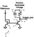
Referring to FIG. 8, one prophetic example of the system 10′ is now described. In this embodiment, a current coming from a reference circuit is mirrored thru N-type transistors, e.g. transistor 12′. One leg of this current flows thru a resistor, e.g. resistor 16′, tied from the transistor drain, e.g. transistor drain 14′, to the positive generated voltage. The resulting IR drop creates the positive comparison voltage (Vcomp_pos). Moreover, there is a capacitor, e.g. capacitor 20′, in parallel that provides a high speed path from the generated voltage to the comparison voltage. Thus a change at the generated voltage, regardless of the frequency, will be seen at the comparison.
There is an additional current mirror and resistor/capacitor pair, e.g. resistor 26′/capacitor 30′, to create the negative comparison voltage (Vcomp_neg). Like the positive voltage, this voltage will react to changes on the generated voltage quickly and accurately. It can be shown thru Ohms law that if we compare both comparison voltages to the same reference, the difference between the positive and negative generated voltages in the charge pump system 10′ will remain constant and have no sensitivity to power supply or process. In addition, the current mirrors can be cascoded for more power supply rejection.
The capabilities of the system 10 can be implemented in software, firmware, hardware or some combination thereof.
The flow diagrams depicted herein are just examples. There may be many variations to these diagrams or the steps (or operations) described therein without departing from the spirit of the invention. For instance, the steps may be performed in a differing order, or steps may be added, deleted or modified. All of these variations are considered a part of the claimed invention. Furthermore, the use of the terms a, an, etc. do not denote a limitation of quantity, but rather denote the presence of at least one of the referenced item.
While the preferred embodiment to the invention has been described, it will be understood that those skilled in the art, both now and in the future, may make various improvements and enhancements which fall within the scope of the claims which follow. These claims should be construed to maintain the proper protection for the invention first described.

Claims (7)

1. A system to evaluate a voltage in a charge pump, the system comprising:
a transistor;
a transistor drain carried by said transistor, said transistor drain receiving a reference current;
a transistor gate carried by said transistor and connected to said transistor drain;
an additional transistor;
an additional transistor gate carried by said additional transistor and connected to said transistor gate;
an additional transistor drain to receive the reference current mirrored from said additional transistor;
a resistor;
a node between said resistor and said additional transistor drain to establish a comparison voltage based upon the mirrored reference current; and
a capacitor in parallel with said resistor.
2. The system of claim 1 wherein said resistor and said additional transistor drain have only said node between them.
3. The system of claim 1 wherein said resistor receives the mirrored reference current.
4. The system of claim 1 wherein said transistor and said additional transistor comprise n-type transistors.
5. A method of evaluating a voltage in a charge pump, the method comprising:
receiving a reference current at a transistor drain;
mirroring a current using an additional transistor;
receiving a mirrored current at a resistor;
establishing a comparison voltage based upon the mirrored current at a node between the resistor and the additional transistor drain; and
providing a capacitor in parallel with the resistor.
6. A system to evaluate a voltage in a charge pump, the system comprising:
a transistor;
a transistor drain carried by said transistor, said transistor drain receiving a reference current;
a transistor gate carried by said transistor and connected to said transistor drain;
an additional transistor;
an additional transistor gate carried by said additional transistor and connected to said transistor gate;
an additional transistor drain to receive the reference current mirrored from said additional transistor;
a resistor;
a node between said resistor and said additional transistor drain to establish a comparison voltage based upon the mirrored reference current and said resistor and said additional transistor drain have only said node between them; and
a capacitor in parallel with said resistor.
7. The system of claim 6 wherein said resistor receives the mirrored reference current.
US12/168,139 2008-07-06 2008-07-06 System to evaluate a voltage in a charge pump and associated methods Expired - Fee Related US7692480B2 (en)

Priority Applications (1)

Application Number Priority Date Filing Date Title
US12/168,139 US7692480B2 (en) 2008-07-06 2008-07-06 System to evaluate a voltage in a charge pump and associated methods

Applications Claiming Priority (1)

Application Number Priority Date Filing Date Title
US12/168,139 US7692480B2 (en) 2008-07-06 2008-07-06 System to evaluate a voltage in a charge pump and associated methods

Publications (2)

Publication Number Publication Date
US20100001766A1 US20100001766A1 (en) 2010-01-07
US7692480B2 true US7692480B2 (en) 2010-04-06

Family

ID=41463888

Family Applications (1)

Application Number Title Priority Date Filing Date
US12/168,139 Expired - Fee Related US7692480B2 (en) 2008-07-06 2008-07-06 System to evaluate a voltage in a charge pump and associated methods

Country Status (1)

Country Link
US (1) US7692480B2 (en)

Cited By (3)

* Cited by examiner, † Cited by third party
Publication number Priority date Publication date Assignee Title
US8436670B2 (en) 2011-01-13 2013-05-07 Micron Technology, Inc. Power supply induced signal jitter compensation
US20130141151A1 (en) * 2011-06-10 2013-06-06 Ramtron International Corporation Analog delay cells for the power supply of an rfid tag
US9250271B2 (en) 2013-08-26 2016-02-02 Globalfoundries Inc. Charge pump generator with direct voltage sensor

Families Citing this family (2)

* Cited by examiner, † Cited by third party
Publication number Priority date Publication date Assignee Title
US8830776B1 (en) * 2013-03-15 2014-09-09 Freescale Semiconductor, Inc. Negative charge pump regulation
CN115309231A (en) * 2021-05-08 2022-11-08 长鑫存储技术有限公司 Comparison circuit and negative voltage generation system

Citations (12)

* Cited by examiner, † Cited by third party
Publication number Priority date Publication date Assignee Title
US3602799A (en) 1970-06-24 1971-08-31 Westinghouse Electric Corp Temperature stable constant current source
US4931844A (en) 1988-03-09 1990-06-05 Ixys Corporation High power transistor with voltage, current, power, resistance, and temperature sensing capability
US5045773A (en) 1990-10-01 1991-09-03 Motorola, Inc. Current source circuit with constant output
US5519310A (en) 1993-09-23 1996-05-21 At&T Global Information Solutions Company Voltage-to-current converter without series sensing resistor
US6285622B1 (en) 1999-10-29 2001-09-04 Mitsubishi Denki Kabushiki Kaisha Semiconductor device
US6424578B2 (en) 2000-05-30 2002-07-23 Samsung Electronics Co., Ltd. Voltage detecting circuit for semiconductor memory device
US6919756B2 (en) 2003-04-30 2005-07-19 Micron Technology, Inc. Method and circuit for adjusting a voltage upon detection of a command applied to an integrated circuit
US6980047B1 (en) * 2002-06-20 2005-12-27 Taiwan Semiconductor Manufacturing Company Low power high voltage ramp-up control circuit
US7068114B2 (en) * 2003-08-07 2006-06-27 Sanyo Electric Co., Ltd. Constant current circuit used for ring oscillator and charge pump circuit
US7109782B2 (en) * 2004-10-05 2006-09-19 Freescale Semiconductor, Inc. Well bias voltage generator
US7224207B2 (en) * 2005-09-20 2007-05-29 Taiwan Semiconductor Manufacturing Co. Charge pump system with smooth voltage output
US7486128B2 (en) * 2005-07-21 2009-02-03 Novatek Microelectronics Corp. Charge pump control circuit and control method thereof

Patent Citations (12)

* Cited by examiner, † Cited by third party
Publication number Priority date Publication date Assignee Title
US3602799A (en) 1970-06-24 1971-08-31 Westinghouse Electric Corp Temperature stable constant current source
US4931844A (en) 1988-03-09 1990-06-05 Ixys Corporation High power transistor with voltage, current, power, resistance, and temperature sensing capability
US5045773A (en) 1990-10-01 1991-09-03 Motorola, Inc. Current source circuit with constant output
US5519310A (en) 1993-09-23 1996-05-21 At&T Global Information Solutions Company Voltage-to-current converter without series sensing resistor
US6285622B1 (en) 1999-10-29 2001-09-04 Mitsubishi Denki Kabushiki Kaisha Semiconductor device
US6424578B2 (en) 2000-05-30 2002-07-23 Samsung Electronics Co., Ltd. Voltage detecting circuit for semiconductor memory device
US6980047B1 (en) * 2002-06-20 2005-12-27 Taiwan Semiconductor Manufacturing Company Low power high voltage ramp-up control circuit
US6919756B2 (en) 2003-04-30 2005-07-19 Micron Technology, Inc. Method and circuit for adjusting a voltage upon detection of a command applied to an integrated circuit
US7068114B2 (en) * 2003-08-07 2006-06-27 Sanyo Electric Co., Ltd. Constant current circuit used for ring oscillator and charge pump circuit
US7109782B2 (en) * 2004-10-05 2006-09-19 Freescale Semiconductor, Inc. Well bias voltage generator
US7486128B2 (en) * 2005-07-21 2009-02-03 Novatek Microelectronics Corp. Charge pump control circuit and control method thereof
US7224207B2 (en) * 2005-09-20 2007-05-29 Taiwan Semiconductor Manufacturing Co. Charge pump system with smooth voltage output

Cited By (7)

* Cited by examiner, † Cited by third party
Publication number Priority date Publication date Assignee Title
US8436670B2 (en) 2011-01-13 2013-05-07 Micron Technology, Inc. Power supply induced signal jitter compensation
US8779822B2 (en) 2011-01-13 2014-07-15 Micron Technology, Inc. Power supply induced signal jitter compensation
US9202542B2 (en) 2011-01-13 2015-12-01 Micron Technology, Inc. Power supply induced signal jitter compensation
US20130141151A1 (en) * 2011-06-10 2013-06-06 Ramtron International Corporation Analog delay cells for the power supply of an rfid tag
US8669801B2 (en) * 2011-06-10 2014-03-11 Cypress Semiconductor Corporation Analog delay cells for the power supply of an RFID tag
US9250271B2 (en) 2013-08-26 2016-02-02 Globalfoundries Inc. Charge pump generator with direct voltage sensor
US9341655B2 (en) 2013-08-26 2016-05-17 Globalfoundries Inc. Charge pump generator with direct voltage sensor

Also Published As

Publication number Publication date
US20100001766A1 (en) 2010-01-07

Similar Documents

Publication Publication Date Title
US9525407B2 (en) Power monitoring circuit, and a power up reset generator
US7692480B2 (en) System to evaluate a voltage in a charge pump and associated methods
CN104252192B (en) The control mode of voltage detector, electronic equipment and voltage detector
EP3293688A1 (en) Method and system for matching service scene
JPH11317089A (en) High voltage generating circuit
US9589630B2 (en) Low voltage current reference generator for a sensing amplifier
US20130221987A1 (en) Static noise margin monitoring circuit and method
US20130043889A1 (en) Capacitance evaluation apparatuses and methods
TWI537701B (en) Drain regulator
CN100419911C (en) Power-up circuit in semiconductor memory device
KR20130072137A (en) Voltage regulator
CN110147290B (en) Chip age judging method and device, chip and terminal
US20100001709A1 (en) System to generate a reference for a charge pump and associated methods
CN108389598B (en) Sensitive amplifier circuit clamped by phase inverter
US20100001788A1 (en) System to evaluate charge pump outputs and associated methods
US20200072878A1 (en) Apparatus and system of a low-voltage detector
US7583107B2 (en) Sense amplifier circuit for low voltage applications
JP6847997B2 (en) Low self-consumption power-on reset circuit
US9667240B2 (en) Systems and methods for starting up analog circuits
KR100633598B1 (en) Half power voltage generator
US8258758B2 (en) System to improve a multistage charge pump and associated methods
CN109003634B (en) Chip starting method and FLASH chip
US9263096B1 (en) Voltage comparator circuit and usage thereof
US10832756B1 (en) Negative voltage generation for computer memory
US20100002478A1 (en) System to improve a voltage multiplier and associated methods

Legal Events

Date Code Title Description
AS Assignment

Owner name: INTERNATIONAL BUSINESS MACHINES CORPORATION, NEW Y

Free format text: ASSIGNMENT OF ASSIGNORS INTEREST;ASSIGNORS:GEBARA, FADI H.;KUANG, JENTE B.;MUENCH, PAUL D.;AND OTHERS;REEL/FRAME:021197/0007;SIGNING DATES FROM 20080627 TO 20080701

Owner name: INTERNATIONAL BUSINESS MACHINES CORPORATION,NEW YO

Free format text: ASSIGNMENT OF ASSIGNORS INTEREST;ASSIGNORS:GEBARA, FADI H.;KUANG, JENTE B.;MUENCH, PAUL D.;AND OTHERS;SIGNING DATES FROM 20080627 TO 20080701;REEL/FRAME:021197/0007

FEPP Fee payment procedure

Free format text: PAYER NUMBER DE-ASSIGNED (ORIGINAL EVENT CODE: RMPN); ENTITY STATUS OF PATENT OWNER: LARGE ENTITY

Free format text: PAYOR NUMBER ASSIGNED (ORIGINAL EVENT CODE: ASPN); ENTITY STATUS OF PATENT OWNER: LARGE ENTITY

REMI Maintenance fee reminder mailed
LAPS Lapse for failure to pay maintenance fees
STCH Information on status: patent discontinuation

Free format text: PATENT EXPIRED DUE TO NONPAYMENT OF MAINTENANCE FEES UNDER 37 CFR 1.362

FP Lapsed due to failure to pay maintenance fee

Effective date: 20140406