US7700941B2 - Surface-emitting semiconductor laser comprising a structured waveguide - Google Patents
Surface-emitting semiconductor laser comprising a structured waveguide Download PDFInfo
- Publication number
- US7700941B2 US7700941B2 US11/401,587 US40158706A US7700941B2 US 7700941 B2 US7700941 B2 US 7700941B2 US 40158706 A US40158706 A US 40158706A US 7700941 B2 US7700941 B2 US 7700941B2
- Authority
- US
- United States
- Prior art keywords
- layer
- semiconductor laser
- doped
- raised portion
- laser according
- Prior art date
- Legal status (The legal status is an assumption and is not a legal conclusion. Google has not performed a legal analysis and makes no representation as to the accuracy of the status listed.)
- Active, expires
Links
Images


Classifications
-
- H—ELECTRICITY
- H01—ELECTRIC ELEMENTS
- H01S—DEVICES USING THE PROCESS OF LIGHT AMPLIFICATION BY STIMULATED EMISSION OF RADIATION [LASER] TO AMPLIFY OR GENERATE LIGHT; DEVICES USING STIMULATED EMISSION OF ELECTROMAGNETIC RADIATION IN WAVE RANGES OTHER THAN OPTICAL
- H01S5/00—Semiconductor lasers
- H01S5/10—Construction or shape of the optical resonator, e.g. extended or external cavity, coupled cavities, bent-guide, varying width, thickness or composition of the active region
- H01S5/18—Surface-emitting [SE] lasers, e.g. having both horizontal and vertical cavities
- H01S5/183—Surface-emitting [SE] lasers, e.g. having both horizontal and vertical cavities having only vertical cavities, e.g. vertical cavity surface-emitting lasers [VCSEL]
- H01S5/18308—Surface-emitting [SE] lasers, e.g. having both horizontal and vertical cavities having only vertical cavities, e.g. vertical cavity surface-emitting lasers [VCSEL] having a special structure for lateral current or light confinement
-
- H—ELECTRICITY
- H01—ELECTRIC ELEMENTS
- H01S—DEVICES USING THE PROCESS OF LIGHT AMPLIFICATION BY STIMULATED EMISSION OF RADIATION [LASER] TO AMPLIFY OR GENERATE LIGHT; DEVICES USING STIMULATED EMISSION OF ELECTROMAGNETIC RADIATION IN WAVE RANGES OTHER THAN OPTICAL
- H01S5/00—Semiconductor lasers
- H01S5/02—Structural details or components not essential to laser action
- H01S5/024—Arrangements for thermal management
- H01S5/02469—Passive cooling, e.g. where heat is removed by the housing as a whole or by a heat pipe without any active cooling element like a TEC
-
- H—ELECTRICITY
- H01—ELECTRIC ELEMENTS
- H01S—DEVICES USING THE PROCESS OF LIGHT AMPLIFICATION BY STIMULATED EMISSION OF RADIATION [LASER] TO AMPLIFY OR GENERATE LIGHT; DEVICES USING STIMULATED EMISSION OF ELECTROMAGNETIC RADIATION IN WAVE RANGES OTHER THAN OPTICAL
- H01S5/00—Semiconductor lasers
- H01S5/10—Construction or shape of the optical resonator, e.g. extended or external cavity, coupled cavities, bent-guide, varying width, thickness or composition of the active region
- H01S5/18—Surface-emitting [SE] lasers, e.g. having both horizontal and vertical cavities
- H01S5/183—Surface-emitting [SE] lasers, e.g. having both horizontal and vertical cavities having only vertical cavities, e.g. vertical cavity surface-emitting lasers [VCSEL]
-
- H—ELECTRICITY
- H01—ELECTRIC ELEMENTS
- H01S—DEVICES USING THE PROCESS OF LIGHT AMPLIFICATION BY STIMULATED EMISSION OF RADIATION [LASER] TO AMPLIFY OR GENERATE LIGHT; DEVICES USING STIMULATED EMISSION OF ELECTROMAGNETIC RADIATION IN WAVE RANGES OTHER THAN OPTICAL
- H01S2301/00—Functional characteristics
- H01S2301/16—Semiconductor lasers with special structural design to influence the modes, e.g. specific multimode
- H01S2301/166—Single transverse or lateral mode
-
- H—ELECTRICITY
- H01—ELECTRIC ELEMENTS
- H01S—DEVICES USING THE PROCESS OF LIGHT AMPLIFICATION BY STIMULATED EMISSION OF RADIATION [LASER] TO AMPLIFY OR GENERATE LIGHT; DEVICES USING STIMULATED EMISSION OF ELECTROMAGNETIC RADIATION IN WAVE RANGES OTHER THAN OPTICAL
- H01S2304/00—Special growth methods for semiconductor lasers
-
- H—ELECTRICITY
- H01—ELECTRIC ELEMENTS
- H01S—DEVICES USING THE PROCESS OF LIGHT AMPLIFICATION BY STIMULATED EMISSION OF RADIATION [LASER] TO AMPLIFY OR GENERATE LIGHT; DEVICES USING STIMULATED EMISSION OF ELECTROMAGNETIC RADIATION IN WAVE RANGES OTHER THAN OPTICAL
- H01S5/00—Semiconductor lasers
- H01S5/02—Structural details or components not essential to laser action
- H01S5/024—Arrangements for thermal management
- H01S5/02476—Heat spreaders, i.e. improving heat flow between laser chip and heat dissipating elements
-
- H—ELECTRICITY
- H01—ELECTRIC ELEMENTS
- H01S—DEVICES USING THE PROCESS OF LIGHT AMPLIFICATION BY STIMULATED EMISSION OF RADIATION [LASER] TO AMPLIFY OR GENERATE LIGHT; DEVICES USING STIMULATED EMISSION OF ELECTROMAGNETIC RADIATION IN WAVE RANGES OTHER THAN OPTICAL
- H01S5/00—Semiconductor lasers
- H01S5/04—Processes or apparatus for excitation, e.g. pumping, e.g. by electron beams
- H01S5/042—Electrical excitation ; Circuits therefor
- H01S5/0425—Electrodes, e.g. characterised by the structure
- H01S5/04254—Electrodes, e.g. characterised by the structure characterised by the shape
-
- H—ELECTRICITY
- H01—ELECTRIC ELEMENTS
- H01S—DEVICES USING THE PROCESS OF LIGHT AMPLIFICATION BY STIMULATED EMISSION OF RADIATION [LASER] TO AMPLIFY OR GENERATE LIGHT; DEVICES USING STIMULATED EMISSION OF ELECTROMAGNETIC RADIATION IN WAVE RANGES OTHER THAN OPTICAL
- H01S5/00—Semiconductor lasers
- H01S5/10—Construction or shape of the optical resonator, e.g. extended or external cavity, coupled cavities, bent-guide, varying width, thickness or composition of the active region
- H01S5/18—Surface-emitting [SE] lasers, e.g. having both horizontal and vertical cavities
- H01S5/183—Surface-emitting [SE] lasers, e.g. having both horizontal and vertical cavities having only vertical cavities, e.g. vertical cavity surface-emitting lasers [VCSEL]
- H01S5/18361—Structure of the reflectors, e.g. hybrid mirrors
- H01S5/18369—Structure of the reflectors, e.g. hybrid mirrors based on dielectric materials
-
- H—ELECTRICITY
- H01—ELECTRIC ELEMENTS
- H01S—DEVICES USING THE PROCESS OF LIGHT AMPLIFICATION BY STIMULATED EMISSION OF RADIATION [LASER] TO AMPLIFY OR GENERATE LIGHT; DEVICES USING STIMULATED EMISSION OF ELECTROMAGNETIC RADIATION IN WAVE RANGES OTHER THAN OPTICAL
- H01S5/00—Semiconductor lasers
- H01S5/20—Structure or shape of the semiconductor body to guide the optical wave ; Confining structures perpendicular to the optical axis, e.g. index or gain guiding, stripe geometry, broad area lasers, gain tailoring, transverse or lateral reflectors, special cladding structures, MQW barrier reflection layers
- H01S5/22—Structure or shape of the semiconductor body to guide the optical wave ; Confining structures perpendicular to the optical axis, e.g. index or gain guiding, stripe geometry, broad area lasers, gain tailoring, transverse or lateral reflectors, special cladding structures, MQW barrier reflection layers having a ridge or stripe structure
- H01S5/2205—Structure or shape of the semiconductor body to guide the optical wave ; Confining structures perpendicular to the optical axis, e.g. index or gain guiding, stripe geometry, broad area lasers, gain tailoring, transverse or lateral reflectors, special cladding structures, MQW barrier reflection layers having a ridge or stripe structure comprising special burying or current confinement layers
-
- H—ELECTRICITY
- H01—ELECTRIC ELEMENTS
- H01S—DEVICES USING THE PROCESS OF LIGHT AMPLIFICATION BY STIMULATED EMISSION OF RADIATION [LASER] TO AMPLIFY OR GENERATE LIGHT; DEVICES USING STIMULATED EMISSION OF ELECTROMAGNETIC RADIATION IN WAVE RANGES OTHER THAN OPTICAL
- H01S5/00—Semiconductor lasers
- H01S5/30—Structure or shape of the active region; Materials used for the active region
- H01S5/305—Structure or shape of the active region; Materials used for the active region characterised by the doping materials used in the laser structure
- H01S5/3095—Tunnel junction
-
- H—ELECTRICITY
- H01—ELECTRIC ELEMENTS
- H01S—DEVICES USING THE PROCESS OF LIGHT AMPLIFICATION BY STIMULATED EMISSION OF RADIATION [LASER] TO AMPLIFY OR GENERATE LIGHT; DEVICES USING STIMULATED EMISSION OF ELECTROMAGNETIC RADIATION IN WAVE RANGES OTHER THAN OPTICAL
- H01S5/00—Semiconductor lasers
- H01S5/30—Structure or shape of the active region; Materials used for the active region
- H01S5/32—Structure or shape of the active region; Materials used for the active region comprising PN junctions, e.g. hetero- or double- heterostructures
- H01S5/323—Structure or shape of the active region; Materials used for the active region comprising PN junctions, e.g. hetero- or double- heterostructures in AIIIBV compounds, e.g. AlGaAs-laser, InP-based laser
- H01S5/3235—Structure or shape of the active region; Materials used for the active region comprising PN junctions, e.g. hetero- or double- heterostructures in AIIIBV compounds, e.g. AlGaAs-laser, InP-based laser emitting light at a wavelength longer than 1000 nm, e.g. InP-based 1300 nm and 1500 nm lasers
-
- Y—GENERAL TAGGING OF NEW TECHNOLOGICAL DEVELOPMENTS; GENERAL TAGGING OF CROSS-SECTIONAL TECHNOLOGIES SPANNING OVER SEVERAL SECTIONS OF THE IPC; TECHNICAL SUBJECTS COVERED BY FORMER USPC CROSS-REFERENCE ART COLLECTIONS [XRACs] AND DIGESTS
- Y10—TECHNICAL SUBJECTS COVERED BY FORMER USPC
- Y10S—TECHNICAL SUBJECTS COVERED BY FORMER USPC CROSS-REFERENCE ART COLLECTIONS [XRACs] AND DIGESTS
- Y10S438/00—Semiconductor device manufacturing: process
- Y10S438/933—Germanium or silicon or Ge-Si on III-V
Definitions
- VSELs Vertical-cavity surface-emitting lasers
- VCSELs are semiconductor lasers in which light emission occurs perpendicularly to the surface of the semiconductor chip.
- Vertical-cavity surface-emitting laser diodes have a plurality of advantages over conventional edge-emitting laser diodes, such as low electrical power consumption, the possibility of directly inspecting the laser diode on the wafer, simple possibilities for coupling to a fiber optic, production of longitudinal single-mode spectra and the possibility of connecting the surface-emitting laser diodes to a two-dimensional matrix.
- VCSELs In the field of fiberoptic communication technology, there is a need, due to wavelength-dependent dispersion and absorption, for VCSELs in a wavelength range from approximately 1.3 to 2 ⁇ m, and in particular for wavelengths of around 1.31 ⁇ m or 1.55 ⁇ m.
- GaAs-based VCSELs are suitable for the short-wavelength range of less than 1.3 ⁇ m.
- the lateral beam profile of laser diodes may be influenced to a significant extent by the definition of the corresponding waveguide.
- the waveguiding is produced by selectively oxidised Al(Ga)As layers (cf. “Electrically Pumped 10 Gbit/s MOVPE Grown Monolithic 1.3 ⁇ m VCSEL with GaInNAs Active Region”, Electronics Letters, Vol. 38, No. 7 (28 Mar. 2002), pages 322 to 324).
- MBE Molecular Beam Epitaxy
- the tunnel contact 103 is formed between these two layers.
- a circular or elliptical region which is formed substantially by the n + -doped layer 102 , the tunnel contact 103 and a portion of or the entire p + -doped layer 101 , is shaped by Reactive Ion Etching (RIE).
- RIE Reactive Ion Etching
- this region is overgrown with n-doped InP (layer 104 ), so the tunnel contact is “buried”.
- the contact region between the overgrown layer 104 and the p + -doped layer 101 acts as a barrier layer on application of a voltage.
- the current flows through the tunnel contact at resistances of typically 3 ⁇ 10 ⁇ 6 ⁇ cm 2 .
- the flow of current can thus be restricted to the actual region of the active zone 108 .
- the amount of heat generated is also low, as the current flows from a high-resistance p-doped layer to a low-resistance n-doped layer.
- the overgrowing of the tunnel contact leads to slight variations in thickness of the layers located thereabove, as illustrated in FIG. 2 , and this has a detrimental effect on lateral waveguiding.
- the formation of higher lateral modes is facilitated, especially in relatively large apertures. Only small apertures, and a correspondingly low laser power, may therefore be used for the single-mode operation of conventional VCSELs; this mode is required, for example, in fiberoptic communication technology.
- the buried tunnel junction (BTJ) is inverted relative to FIG. 1 , so the active zone 106 is located above the tunnel contact, which has a diameter D BTJ and is disposed between the p + -doped layer 101 and the n + -doped 102 .
- the laser radiation emerges in the direction indicated by arrow 116 .
- the active zone 106 is surrounded by a p-doped layer 105 (for example, InAlAs) and by an n-doped layer 108 (for example, InAlAs).
- the leading-side mirror 109 above the active zone 106 consists of an epitaxial DBR (Distributed Bragg Reflector) comprising approximately 35 InGa(Al)As/InAlAs layer pairs, thus producing a reflectivity of approximately 99.4%.
- the trailing-side mirror 112 consists of a stack of dielectric layers as the DBR and is completed by a gold layer, thus producing a reflectivity of almost 99.75%.
- An insulating layer 113 is used for lateral insulation.
- An annularly structured further p-side contact layer 111 is provided between the layer 104 and the contact layer 114 .
- FIG. 2 illustrates the manner in which the structure of the overgrown tunnel contact is propagated (in this case, downwardly) into the further layers.
- the combination of the dielectric mirror 112 and the integrated contact layer 114 and the heat sink 115 results in a markedly increased thermal conductivity compared to epitaxial multilayer structures.
- Current is injected via the contact layer 114 or via the integrated heat sink 115 and the n-side contact points 110 .
- a VCSEL having the structure illustrated in FIG. 2 forms the subject-matter of the publication “Low-Threshold Index-Guided 1.5 ⁇ m Long-Wavelength Vertical-Cavity Surface-Emitting Laser with High Efficiency”, Applied Physics Letters, Vol. 76, No. 16 (17 Apr. 2000), pages 2179 to 2181.
- a VCSEL of the same type having an output power of up to 7 mW (20° C., CW) is presented in “Vertical-Cavity Surface-Emitting Laser Diodes at 1.55 ⁇ m with Large Output Power and High Operation Temperature”, Electronics Letters, Vol. 37, No. 21 (11 Oct. 2001), pages 1295 to 1296.
- a VCSEL having an emission wavelength of 2.01 ⁇ m is known from “Electrically Pumped Room Temperature CW-VCSELs with Emission Wavelengths of 2 ⁇ m”, Electronics Letters, Vol. 39, No. 1 (9 Jan. 2003), pages 57 to 58.
- the lateral oxidation method may not be used in the BTJ-VCSELs under discussion, since the materials that are used have excessively low aluminium contents, and other conceivable materials, such as AlAsSb, have, to date, not yielded oxide layers of sufficient quality.
- the lateral waveguiding resulting from the production process accordingly takes place by lateral variation of the length of the resonator.
- selectively etched-off layers cf.
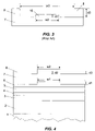
- FIG. 3 illustrates schematically and not to scale the conditions in a known structure of a generic surface-emitting semiconductor laser.
- the diagram shows the borderline region between the current-carrying layer 7 and an n-doped contact layer 8 having a thickness d 3 , through which the current is generally supplied and which has preferably grown onto the layer 7 from highly n-doped InGaAs.
- the contact layer 8 is conventionally applied in an epitaxy step and removed by selective etching in the region of the raised portion 15 .
- the structured contact layer 8 typically has a thickness d 3 from 50 to 100 nm, to ensure low contact resistances, and, at its inner edge, is at a distance of a plurality of micrometers (typically 4 to 5 ⁇ m) from the tunnel contact raised portion 15 .
- the length of the resonator is greater by d 2 in the center than in the regions outside the raised portion 15 .
- the effective index of refraction is higher (typically by 1%) in the center than in the outer region, thus resulting in strong index guiding. This favours the formation of higher modes, especially in large apertures.
- An object of the presently described surface-emitting semiconductor lasers is to replace the index guiding, which, in the case of BTJ-VCSELs, is conventionally strong and favors multimode operation, with a weaker index guiding or gain guiding, and also optionally to damp higher lateral modes.
- the adjustment of the lateral mode profile should allow a single-mode operation even in large apertures having higher single-mode powers than in conventional BTJ-VCSELs.
- a surface-emitting semiconductor laser includes an active zone, the active zone having a p-n-junction and surrounded by a first n-doped semiconductor layer and at least one p-doped semiconductor layer; a tunnel contact layer on the p-side of the active zone; an n-doped current-carrying layer that covers the tunnel contact layer, the n-doped current-carrying layer comprising a raised portion; and a structured layer having an optical thickness at least equal to the optical thickness of the current-carrying layer in the region of the raised portion, wherein the structured layer is disposed on the current-carrying layer within a maximum distance of 2 ⁇ m from the raised portion.
- FIG. 1 is a schematic illustration of the structure of a buried tunnel contact in a known surface-emitting semiconductor laser.
- FIG. 2 is a schematic illustration of a complete structure of a known surface-emitting semiconductor laser.
- FIG. 3 is a schematic illustration of a contact layer and current-carrying layer in a known structure of a surface-emitting semiconductor laser.
- FIG. 4 shows a structure formed during the production of a surface-emitting semiconductor laser according to one embodiment.
- FIG. 5 is a schematic illustration of a contact layer forming a structured layer according to one embodiment.
- FIG. 6 illustrates a structured layer provided next to a contact layer according to one embodiment.
- FIG. 7 shows a structure formed during the production of a surface-emitting semiconductor laser having an antiguiding effect according to one embodiment.
- FIG. 8 shows a surface-emitting semiconductor laser according to one embodiment.
- a structured layer the optical thickness of which is at least equal to the optical thickness of the current-carrying layer 7 in the region of the raised portion 15 , i.e. to the optical thickness of the raised portion 15 having the thickness d 2 .
- the structured layer therefore compensates differences in the index of refraction in the center and outer regions of the raised portion 15 , as a result of which the index guiding is markedly weakened.
- the structured layer is either adjacent to the raised portion 15 or within a specific maximum distance from the raised portion. It has been found that this maximum distance should be no more than 2 ⁇ m, but preferably no more than 1 ⁇ m. This maximum distance therefore corresponds to 40 to 50%, preferably 20 to 25%, of the previous typical distance of the (optional) contact layer 8 from the outer edge of the raised portion 15 (cf. FIG. 3 ).
- the structured layer is an n-doped contact layer.
- the thickness of the contact layer is such that its optical thickness is, for example, equal to the optical thickness of the current-carrying layer in the region of the raised portion 15 of depth d 2 (cf. FIG. 3 ), where for sufficient influencing of the optical field, the contact layer should be no further than 1 to 2 ⁇ m from the raised portion.
- the structured layer is provided independently of the optional contact layer.
- the material from which the structured layer is made may be freely selected, and the layer is preferably directly adjacent to the raised portion in the current-carrying layer. The distance from the raised portion and the thickness of this structured layer are as described above with reference to the embodiment where the contact layer forms the structured layer.
- the material may, in particular, be selected to damp higher modes, at the edge of the aperture where they have stronger field extensions, thus preventing these modes from oscillating.
- Materials having a marked absorbing effect for each wavelength are, in general, suitable for this purpose. For wavelengths between 1.3 and 1.55 ⁇ m, amorphous silicon is particularly suitable. Titanium is, for example, suitable for the entire conventional wavelength range.
- a contact layer surrounding the structured layer may also be provided.
- the geometry of said contact layer is substantially freely selectable, as the waveguide effect is already compensated by the structured layer.
- the presently described surface-emitting semiconductor lasers allow the index guiding not only to be weakened, but also to be converted, thus producing an antiguiding effect, which also eliminates higher modes.
- the (optical) thickness of the structured layer is therefore selected so as to be significantly greater than the depth of the raised portion caused by the tunnel contact. A raised portion is thus produced in the outer region, where if the structured layer has an absorbing effect, the elimination of higher modes is even more effective.
- the structured layer that is used may, again, be an n-doped contact layer or a combination of a layer, the material of which may be freely selected, as the structured layer and an optional additional contact layer.
- FIG. 4 shows the example of a structure formed during the production of a surface-emitting semiconductor laser.
- an n-doped epitaxial Bragg mirror 2 Starting from an InP substrate 1 , an n-doped epitaxial Bragg mirror 2 , an n-doped confinement layer 3 , an active zone 4 and a p-doped confinement layer 5 are successively applied in a first epitaxial growth process.
- the structure is completed by the growth of a tunnel contact layer 6 consisting, for example, in each case of a highly p + - and n + -doped InGaAs layer.
- An aperture the dimensions of which may be freely selected and which either extends to the layer 5 or ends within the p-doped portion of layer 6 , is formed in the subsequent lithographic and etching process. Typical etching depths are, in this case, 20 nm.
- an upper n-doped current-supplying layer 7 preferably consisting of InP
- an optional n-contact layer 8 preferably consisting of highly n-doped InGaAs grown to a thickness d 3 .
- the lateral semiaxis ratio may be modified or maintained, depending on the process parameters and the epitaxy method (for example, MBE (Molecular Beam Epitaxy), CBE (Chemical Beam Epitaxy) or MOVPE (Metal Organic Vapour Phase Epitaxy)).
- MBE Molecular Beam Epitaxy
- CBE Chemical Beam Epitaxy
- MOVPE Metal Organic Vapour Phase Epitaxy
- FIG. 4 The result is shown in FIG. 4 , in which, for example, a round aperture having the diameter w 1 is taken as a lithographically defined aperture having an etching depth d 1 , which, after the overgrowing process, has a diameter w 2 with a height d 2 .
- the values w 2 and d 2 generally correspond to the starting data w 1 and d 1 .
- apertures other than circular ones may also be used, so the terms “diameter” or “radius”, as used herein, do not entail any limitation to circular aperture geometries. Angular, elliptical or any other geometries are also possible, and the disclosed instrumentalities may be transferred to such geometries.
- the contact layer 8 acts as the structured layer.
- the thickness d 3 of the contact layer is, for example, selected, for complete compensation of the waveguide effect, in such a way that its optical thickness corresponds to the optical thickness in the region of the etching depth d 2 of layer 7 .
- An almost plane-parallel arrangement is then obtained.
- the etching diameter w 3 may be adjusted in almost any desired manner.
- the radius should, however, typically be no more than 1 ⁇ m greater than the radius of the tunnel contact. Further advantageous maximum distances include 0, 0.1, 0.2, 0.3, 0.4, 0.5, 0.6, 0.7, 0.8 and 0.9 ⁇ m.
- FIG. 5 shows clearly the different conditions achieved by the presently described surface-emitting semiconductor lasers compared to the prior art conditions illustrated in FIG. 3 .
- the presently described structuring causes balancing of the effective index of refraction from the center into the outer regions of the aperture. As a result, the strong index guiding present in FIG. 3 is replaced by weak index guiding.
- FIG. 6 shows another embodiment of a waveguide structure.
- the contact layer 8 is provided only optionally and may in this case be selectively structured, in a similar manner to that described above, with an opening diameter w 3 .
- the waveguide characteristics are, in this case, influenced through an additional layer 9 , which may be made from a freely selectable material.
- Layer 9 has an internal diameter w 4 and an external diameter w 5 , and is structured, for example, by etching processes or a lift-off method. The same principle applies to the dimensions of the thickness d 4 and the internal diameter w 4 as in the case of the contact layer as the structured layer ( FIG. 5 ).
- An advantage of this embodiment is the free selection of the material of the structured layer 9 . This may, in particular, be used to damp more intense higher modes, which usually have their maximum values at the edge of the aperture, thus preventing these modes from oscillating.
- Amorphous silicon is a suitable material for the layer 9 .
- FIG. 7 shows another embodiment of the waveguide structure, which has an antiguiding effect.
- This embodiment is similar to that described in FIG. 5 , although in this case the thickness d 3 of the contact layer 8 , as the structured layer, is selected so as to be significantly greater than the raised portion depth d 2 or etching depth d 1 of the tunnel contact. This results in heightening of the outer region, leading to an antiguiding effect and also eliminating higher modes. If the layer 8 has an absorbing effect, the elimination of the modes is even more effective.
- This embodiment illustrated in FIG. 7 may also be combined with the structure shown in FIG. 6 . In this case, at least the layer 9 comprises the illustrated raised portion.
- FIG. 8 shows the finished BTJ-VCSEL including a surface-emitting semiconductor laser as described herein.
- the further processing of the structure for forming the finished semiconductor laser has already been described in detail in relation to FIG. 2 in the introductory part of the description.
- Identical reference numerals denote the same layers as in the structure according to FIG. 4 .
- the InP substrate 1 is, in this case, entirely removed. Instead, an n-side contact 14 consisting, for example, of Ti/Pt/Au is attached to the current supply means.
- the waveguide structure of the semiconductor laser illustrated in FIG. 8 corresponds to that from FIG. 5 with a contact layer 8 adjacent to the raised portion 15 .
- 10 denotes an insulating and passivation layer, 11 the p-side contact (for example, Ti/Pt/Au), 12 the dielectric mirror, and 13 the integrated heat sink.
- the production of BTJ-VCSELs having high single-mode power has been described.
- the aperture diameters may be enlarged to increase the power, without higher modes being stimulated.
Landscapes
- Physics & Mathematics (AREA)
- Condensed Matter Physics & Semiconductors (AREA)
- General Physics & Mathematics (AREA)
- Electromagnetism (AREA)
- Optics & Photonics (AREA)
- Semiconductor Lasers (AREA)
Abstract
Description
Claims (16)
Applications Claiming Priority (5)
| Application Number | Priority Date | Filing Date | Title |
|---|---|---|---|
| DE10348211 | 2003-10-16 | ||
| DEDE10348211.3 | 2003-10-16 | ||
| DEDE10353960.3 | 2003-11-19 | ||
| DE10353960A DE10353960B4 (en) | 2003-10-16 | 2003-11-19 | Surface-emitting semiconducting laser with structured waveguide has structured layer about lateral area of elevation with thickness selected so its optical thickness is at least equal to that of current carrying layer near elevation depth |
| PCT/EP2004/011569 WO2005039003A1 (en) | 2003-10-16 | 2004-10-14 | Surface-emitting semiconductor laser comprising a structured waveguide |
Related Parent Applications (1)
| Application Number | Title | Priority Date | Filing Date |
|---|---|---|---|
| PCT/EP2004/011569 Continuation WO2005039003A1 (en) | 2003-10-16 | 2004-10-14 | Surface-emitting semiconductor laser comprising a structured waveguide |
Publications (2)
| Publication Number | Publication Date |
|---|---|
| US20060249738A1 US20060249738A1 (en) | 2006-11-09 |
| US7700941B2 true US7700941B2 (en) | 2010-04-20 |
Family
ID=34466021
Family Applications (1)
| Application Number | Title | Priority Date | Filing Date |
|---|---|---|---|
| US11/401,587 Active 2025-11-28 US7700941B2 (en) | 2003-10-16 | 2006-04-11 | Surface-emitting semiconductor laser comprising a structured waveguide |
Country Status (10)
| Country | Link |
|---|---|
| US (1) | US7700941B2 (en) |
| EP (1) | EP1676346B1 (en) |
| JP (1) | JP2007508702A (en) |
| KR (1) | KR20060089740A (en) |
| CN (1) | CN1868099A (en) |
| AT (1) | ATE357760T1 (en) |
| CA (1) | CA2541776A1 (en) |
| DE (2) | DE10353960B4 (en) |
| IL (1) | IL174806A0 (en) |
| WO (1) | WO2005039003A1 (en) |
Families Citing this family (6)
| Publication number | Priority date | Publication date | Assignee | Title |
|---|---|---|---|---|
| US6800287B2 (en) | 1998-09-25 | 2004-10-05 | Yeda Research And Development Co., Ltd. | Copolymer 1 related polypeptides for use as molecular weight markers and for therapeutic use |
| WO2006029393A2 (en) | 2004-09-09 | 2006-03-16 | Teva Pharmaceutical Industries, Ltd. | Process for preparation of mixtures of polypeptides using purified hydrobromic acid |
| JP4895993B2 (en) | 2007-12-26 | 2012-03-14 | ソニー株式会社 | Light emitting device assembly and method for manufacturing the same |
| JP2009283703A (en) * | 2008-05-22 | 2009-12-03 | Sumitomo Electric Ind Ltd | Face emission type laser element and its manufacturing method |
| US10892601B2 (en) * | 2018-05-24 | 2021-01-12 | Stanley Electric Co., Ltd. | Vertical cavity light-emitting element |
| WO2023162488A1 (en) * | 2022-02-25 | 2023-08-31 | ソニーグループ株式会社 | Surface emitting laser, light source device, and ranging device |
Citations (9)
| Publication number | Priority date | Publication date | Assignee | Title |
|---|---|---|---|---|
| US6052398A (en) * | 1997-04-03 | 2000-04-18 | Alcatel | Surface emitting semiconductor laser |
| US20020003823A1 (en) * | 2000-03-24 | 2002-01-10 | Hiroshi Yoshida | Semiconductor laser light emitting device |
| US6366595B1 (en) * | 1997-12-31 | 2002-04-02 | Corning Lasertron, Inc. | Semiconductor laser with kink suppression layer |
| WO2002065599A2 (en) * | 2001-02-15 | 2002-08-22 | Vertilas Gmbh | Surface-emitting semiconductor laser |
| US6717972B2 (en) * | 2000-02-02 | 2004-04-06 | Infineon Technologies Ag | VCSEL with monolithically integrated photodetector |
| WO2004049461A2 (en) * | 2002-11-27 | 2004-06-10 | Vertilas Gmbh | Method for producing a buried tunnel junction in a surface-emitting semiconductor laser |
| US6897993B2 (en) * | 2001-07-24 | 2005-05-24 | Infineon Technologies Ag | Electroabsorption modulator, modulator laser device and method for producing an electroabsorption modulator |
| US6977424B1 (en) * | 2002-03-18 | 2005-12-20 | Finisar Corporation | Electrically pumped semiconductor active region with a backward diode, for enhancing optical signals |
| US7103080B2 (en) * | 2002-03-04 | 2006-09-05 | Quintessence Photonics Corp. | Laser diode with a low absorption diode junction |
Family Cites Families (4)
| Publication number | Priority date | Publication date | Assignee | Title |
|---|---|---|---|---|
| US6931042B2 (en) * | 2000-05-31 | 2005-08-16 | Sandia Corporation | Long wavelength vertical cavity surface emitting laser |
| DE10038235A1 (en) * | 2000-08-04 | 2002-02-21 | Osram Opto Semiconductors Gmbh | Surface emitting laser with side current injection |
| US6839370B2 (en) * | 2001-12-31 | 2005-01-04 | Agilent Technologies, Inc. | Optoelectronic device using a disabled tunnel junction for current confinement |
| DE10317970B4 (en) * | 2003-02-04 | 2005-12-22 | Vertilas Gmbh | A method of fabricating a waveguide structure in a surface emitting semiconductor laser and surface emitting semiconductor laser |
-
2003
- 2003-11-19 DE DE10353960A patent/DE10353960B4/en not_active Expired - Lifetime
-
2004
- 2004-10-14 KR KR1020067007420A patent/KR20060089740A/en not_active Application Discontinuation
- 2004-10-14 DE DE502004003310T patent/DE502004003310D1/en active Active
- 2004-10-14 EP EP04790425A patent/EP1676346B1/en active Active
- 2004-10-14 JP JP2006534688A patent/JP2007508702A/en not_active Withdrawn
- 2004-10-14 WO PCT/EP2004/011569 patent/WO2005039003A1/en active Search and Examination
- 2004-10-14 AT AT04790425T patent/ATE357760T1/en not_active IP Right Cessation
- 2004-10-14 CN CNA2004800305339A patent/CN1868099A/en active Pending
- 2004-10-14 CA CA002541776A patent/CA2541776A1/en not_active Abandoned
-
2006
- 2006-04-05 IL IL174806A patent/IL174806A0/en unknown
- 2006-04-11 US US11/401,587 patent/US7700941B2/en active Active
Patent Citations (11)
| Publication number | Priority date | Publication date | Assignee | Title |
|---|---|---|---|---|
| US6052398A (en) * | 1997-04-03 | 2000-04-18 | Alcatel | Surface emitting semiconductor laser |
| US6366595B1 (en) * | 1997-12-31 | 2002-04-02 | Corning Lasertron, Inc. | Semiconductor laser with kink suppression layer |
| US6717972B2 (en) * | 2000-02-02 | 2004-04-06 | Infineon Technologies Ag | VCSEL with monolithically integrated photodetector |
| US20020003823A1 (en) * | 2000-03-24 | 2002-01-10 | Hiroshi Yoshida | Semiconductor laser light emitting device |
| WO2002065599A2 (en) * | 2001-02-15 | 2002-08-22 | Vertilas Gmbh | Surface-emitting semiconductor laser |
| US7170917B2 (en) * | 2001-02-15 | 2007-01-30 | Vercilas Gmbh | Surface-emitting semiconductor laser |
| US6897993B2 (en) * | 2001-07-24 | 2005-05-24 | Infineon Technologies Ag | Electroabsorption modulator, modulator laser device and method for producing an electroabsorption modulator |
| US7103080B2 (en) * | 2002-03-04 | 2006-09-05 | Quintessence Photonics Corp. | Laser diode with a low absorption diode junction |
| US6977424B1 (en) * | 2002-03-18 | 2005-12-20 | Finisar Corporation | Electrically pumped semiconductor active region with a backward diode, for enhancing optical signals |
| US20060126687A1 (en) * | 2002-11-12 | 2006-06-15 | Vertilas Gmbh | Method for producing a buried tunnel junction in a surface-emitting semiconductor laser |
| WO2004049461A2 (en) * | 2002-11-27 | 2004-06-10 | Vertilas Gmbh | Method for producing a buried tunnel junction in a surface-emitting semiconductor laser |
Also Published As
| Publication number | Publication date |
|---|---|
| CA2541776A1 (en) | 2005-04-28 |
| JP2007508702A (en) | 2007-04-05 |
| EP1676346B1 (en) | 2007-03-21 |
| WO2005039003A1 (en) | 2005-04-28 |
| EP1676346A1 (en) | 2006-07-05 |
| DE10353960B4 (en) | 2006-03-23 |
| KR20060089740A (en) | 2006-08-09 |
| CN1868099A (en) | 2006-11-22 |
| US20060249738A1 (en) | 2006-11-09 |
| DE502004003310D1 (en) | 2007-05-03 |
| IL174806A0 (en) | 2006-08-20 |
| ATE357760T1 (en) | 2007-04-15 |
| DE10353960A1 (en) | 2005-05-25 |
Similar Documents
| Publication | Publication Date | Title |
|---|---|---|
| Iga | Surface-emitting laser-its birth and generation of new optoelectronics field | |
| Riechert et al. | Development of InGaAsN-based 1.3 μm VCSELs | |
| US6411638B1 (en) | Coupled cavity anti-guided vertical-cavity surface-emitting laser | |
| US8331412B2 (en) | Vertical-cavity surface-emitting semiconductor laser diode and method for the manufacture thereof | |
| US6890778B2 (en) | Vertical cavity surface emitting laser and a method of fabrication thereof | |
| US6727520B2 (en) | Spatially modulated reflector for an optoelectronic device | |
| US7288421B2 (en) | Method for forming an optoelectronic device having an isolation layer | |
| Lin et al. | High temperature continuous-wave operation of 1.3-and 1.55-μm VCSELs with InP/air-gap DBRs | |
| US20070030874A1 (en) | Surface-emitting laser element and laser module using the same | |
| US20050265415A1 (en) | Laser diode and method of manufacture | |
| Gruendl et al. | Record single-mode, high-power VCSELs by inhibition of spatial hole burning | |
| JP5029254B2 (en) | Surface emitting laser | |
| Blokhin et al. | High power single mode 1300-nm superlattice based VCSEL: Impact of the buried tunnel junction diameter on performance | |
| US7700941B2 (en) | Surface-emitting semiconductor laser comprising a structured waveguide | |
| Schiehlen et al. | Diode-pumped semiconductor disk laser with intracavity frequency doubling using lithium triborate (LBO) | |
| Louderback et al. | VCSELs with monolithic coupling to internal horizontal waveguides using integrated diffraction gratings | |
| Ohiso et al. | Single transverse mode operation of 1.55-μm buried heterostructure vertical-cavity surface-emitting lasers | |
| Unold et al. | Large-area single-mode selectively oxidized VCSELs: Approaches and experimental | |
| TW202308247A (en) | Reflector for vcsel | |
| US7376163B2 (en) | Method for producing a waveguide structure in a surface-emitting semiconductor laser and surface-emitting semiconductor laser | |
| US20060126687A1 (en) | Method for producing a buried tunnel junction in a surface-emitting semiconductor laser | |
| Grote et al. | Laser components | |
| Nishiyama et al. | Long-wavelength VCSELs on InP grown by MOCVD | |
| Babichev et al. | Long-Wavelength VCSELs: Status and Prospects. Photonics 2023, 10, 268 | |
| Lin et al. | Vertical-cavity surface-emitting lasers with monolithically integrated horizontal waveguides |
Legal Events
| Date | Code | Title | Description |
|---|---|---|---|
| AS | Assignment |
Owner name: VERTILAS GMBH,GERMANY Free format text: ASSIGNMENT OF ASSIGNORS INTEREST;ASSIGNOR:ORTSIEFER, MARKUS;REEL/FRAME:018077/0963 Effective date: 20060613 Owner name: VERTILAS GMBH,GERMANY Free format text: ASSIGNMENT OF ASSIGNORS INTEREST;ASSIGNOR:ORTSIEFER, MARKUS;REEL/FRAME:018088/0357 Effective date: 20060613 Owner name: VERTILAS GMBH, GERMANY Free format text: ASSIGNMENT OF ASSIGNORS INTEREST;ASSIGNOR:ORTSIEFER, MARKUS;REEL/FRAME:018088/0357 Effective date: 20060613 Owner name: VERTILAS GMBH, GERMANY Free format text: ASSIGNMENT OF ASSIGNORS INTEREST;ASSIGNOR:ORTSIEFER, MARKUS;REEL/FRAME:018077/0963 Effective date: 20060613 |
|
| STCF | Information on status: patent grant |
Free format text: PATENTED CASE |
|
| FPAY | Fee payment |
Year of fee payment: 4 |
|
| MAFP | Maintenance fee payment |
Free format text: PAYMENT OF MAINTENANCE FEE, 8TH YR, SMALL ENTITY (ORIGINAL EVENT CODE: M2552) Year of fee payment: 8 |
|
| MAFP | Maintenance fee payment |
Free format text: PAYMENT OF MAINTENANCE FEE, 12TH YR, SMALL ENTITY (ORIGINAL EVENT CODE: M2553); ENTITY STATUS OF PATENT OWNER: SMALL ENTITY Year of fee payment: 12 |