US7701549B2 - Method and apparatus to prevent contamination of optical element by resist processing - Google Patents
Method and apparatus to prevent contamination of optical element by resist processing Download PDFInfo
- Publication number
- US7701549B2 US7701549B2 US11/512,662 US51266206A US7701549B2 US 7701549 B2 US7701549 B2 US 7701549B2 US 51266206 A US51266206 A US 51266206A US 7701549 B2 US7701549 B2 US 7701549B2
- Authority
- US
- United States
- Prior art keywords
- optical element
- substrate
- gas
- enclosure
- valve
- Prior art date
- Legal status (The legal status is an assumption and is not a legal conclusion. Google has not performed a legal analysis and makes no representation as to the accuracy of the status listed.)
- Active, expires
Links
Images


Classifications
-
- G—PHYSICS
- G03—PHOTOGRAPHY; CINEMATOGRAPHY; ANALOGOUS TECHNIQUES USING WAVES OTHER THAN OPTICAL WAVES; ELECTROGRAPHY; HOLOGRAPHY
- G03B—APPARATUS OR ARRANGEMENTS FOR TAKING PHOTOGRAPHS OR FOR PROJECTING OR VIEWING THEM; APPARATUS OR ARRANGEMENTS EMPLOYING ANALOGOUS TECHNIQUES USING WAVES OTHER THAN OPTICAL WAVES; ACCESSORIES THEREFOR
- G03B27/00—Photographic printing apparatus
- G03B27/32—Projection printing apparatus, e.g. enlarger, copying camera
- G03B27/42—Projection printing apparatus, e.g. enlarger, copying camera for automatic sequential copying of the same original
-
- G—PHYSICS
- G03—PHOTOGRAPHY; CINEMATOGRAPHY; ANALOGOUS TECHNIQUES USING WAVES OTHER THAN OPTICAL WAVES; ELECTROGRAPHY; HOLOGRAPHY
- G03F—PHOTOMECHANICAL PRODUCTION OF TEXTURED OR PATTERNED SURFACES, e.g. FOR PRINTING, FOR PROCESSING OF SEMICONDUCTOR DEVICES; MATERIALS THEREFOR; ORIGINALS THEREFOR; APPARATUS SPECIALLY ADAPTED THEREFOR
- G03F7/00—Photomechanical, e.g. photolithographic, production of textured or patterned surfaces, e.g. printing surfaces; Materials therefor, e.g. comprising photoresists; Apparatus specially adapted therefor
- G03F7/70—Microphotolithographic exposure; Apparatus therefor
- G03F7/708—Construction of apparatus, e.g. environment aspects, hygiene aspects or materials
- G03F7/70908—Hygiene, e.g. preventing apparatus pollution, mitigating effect of pollution or removing pollutants from apparatus
Definitions
- the present invention is directed to integrated circuits and their processing for the manufacture of semiconductor devices. More particularly, the invention provides a method and an apparatus for lithography process for the manufacture of integrated circuits. But it would be recognized that the invention has a much broader range of applicability. For example, the invention can be applied to a variety of devices such as dynamic random access memory devices, static random access memory devices (SRAM), application specific integrated circuit devices (ASIC), microprocessors and microcontrollers, Flash memory devices, and others.
- SRAM static random access memory devices
- ASIC application specific integrated circuit devices
- Flash memory devices and others.
- Integrated circuits or “ICs” have evolved from a handful of interconnected devices fabricated on a single chip of silicon to millions of devices. Current ICs provide performance and complexity far beyond what was originally imagined. In order to achieve improvements in complexity and circuit density (i.e., the number of devices capable of being packed onto a given chip area), the size of the smallest device feature, also known as the device “geometry”, has become smaller with each generation of ICs. Semiconductor devices are now being fabricated with features less than a quarter of a micron across.
- IC fabrication facility can cost hundreds of millions, or even billions, of dollars.
- Each fabrication facility will have a certain throughput of wafers, and each wafer will have a certain number of ICs on it. Therefore, by making the individual devices of an IC smaller, more devices may be fabricated on each wafer, thus increasing the output of the fabrication facility.
- Making devices smaller is very challenging, as each process used in IC fabrication has a limit. That is to say, a given process typically only works down to a certain feature size, and then either the process or the device layout needs to be changed.
- Lithography process includes steps of depositing a photoresist material, patterning and developing the photoresist material.
- the invention provides a method and an apparatus for a lithography process for manufacture of integrated circuits.
- the invention has been applied to a wafer edge expose process step in the lithography process.
- An embodiment of an apparatus in accordance with the present invention for processing a substrate comprises, a process chamber configured to support a substrate therein, a light source, and an optical element in optical communication with the light source and configured to expose selected regions of a substrate to radiation from the light source.
- a gas delivery system is configured to flow a gas proximate to the optical element in order to isolate the optical element from a vapor present during a processing step.
- An embodiment of a method in accordance with the present invention for processing a substrate comprises, forming a resist material on a surface of a substrate, exposing a region of the substrate to radiation through an optical element, and providing a purge gas flow proximate to the optical element, the purge gas flow preventing a vapor from the exposed substrate from depositing solid material on the optical element.
- An embodiment of a method in accordance with the present invention for reducing contamination in a semiconductor fabrication tool comprises, exposing a resist material on a substrate to radiation, and providing a purge gas flow to an optical element disposed proximate to the exposed resist material, such that the purge gas flow prevents a vapor from the exposed resist material from depositing solid material on the optical element.
- FIG. 1( a ) is a simplified cross-sectional view illustrating a conventional apparatus for processing a semiconductor integrated circuit device.
- FIG. 1( b ) is a simplified schematic diagram illustrating use of the conventional apparatus shown in FIG. 1( a ).
- FIG. 1( c ) is a simplified plan view of a wafer undergoing development steps to create a wafer edge expose region.
- FIG. 2( a ) is a simplified schematic diagram illustrating performance of a conventional apparatus for processing a semiconductor integrated circuit device.
- FIG. 2( b ) is a simplified plot illustrating performance of a conventional apparatus for processing a semiconductor integrated circuit device.
- FIG. 3( a ) is a simplified schematic diagram showing an apparatus for processing semiconductor integrated circuits according to an embodiment of the present invention.
- FIG. 3( b ) is a simplified cross-sectional view of an illumination system for a lithography process.
- FIG. 3( c ) is a simplified elevational view of one embodiment of an enclosure in accordance with the present invention.
- FIG. 4( a ) is a simplified cross-sectional diagram illustrating an apparatus for processing semiconductor wafer according to an embodiment of the present invention.
- FIG. 4( b ) is a simplified schematic diagram illustrating an apparatus for processing semiconductor wafer according to an embodiment of the present invention.
- the present invention provides a method and an apparatus for a lithography process for manufacture of integrated circuits.
- the invention has been applied to a wafer edge expose step in a lithography process.
- an apparatus for a lithography process for fabricating semiconductor integrated devices includes providing a process chamber.
- the process chamber may be configured for a track tool for lithography process.
- the apparatus includes an illumination system, the illumination system provides a light source to expose photoresist material on selected regions on a semiconductor substrate.
- the light source can be a ArF laser emitting a ultraviolet light at a wavelength of 193 nm.
- the apparatus includes a fiber optic to direct light from the light source to the semiconductor substrate.
- the apparatus may also include a shutter to control exposure of the photoresist material on selected regions on the semiconductor substrate.
- the apparatus includes an optical element.
- the optical element can be a lens to expose portions of the semiconductor substrate and may comprise material such as calcium fluoride in a specific embodiment.
- the optical element is positioned at an end of the fiber optics and at a distance from the semiconductor substrate. This distance may range from about 0.3-0.5 mm in accordance with certain embodiments.
- the apparatus also includes an enclosure having a first opened ending and a second opened ending. The first opened ending is coupled to the optical element and the second opened ending is positioned above the semiconductor substrate.
- the enclosure is perforated and may be substantially cylindrical.
- the apparatus includes a gas delivery system to provide a gas to flow through the enclosure.
- the gas is provided to isolate the optical element from a vapor component of the photoresist material during exposure in the lithography process and eliminates a solid material from depositing on the optical element, thereby maintaining the intensity of light transmitted through the optical element at a desired level.
- the apparatus may also include a gas control system.
- the gas control system includes a solenoid valve to provide opening/shutting of the shutter, a air-spring valve to control the gas flows through the enclosure, and a three way valve.
- the three way valve is coupled in common to the solenoid valve and the air-spring valve and provides a mean to simultaneously flow the gas through the enclosure and to open the shutter for exposure of the photoresist material.
- a method for fabricating semiconductor integrated circuits includes providing a semiconductor substrate.
- the semiconductor substrate has a surface and may have devices partially fabricated on it.
- a photoresist material is deposited overlying the surface of the semiconductor substrate.
- the method includes disposing the semiconductor substrate on a pedestal of a track tool.
- the method includes directing a ultraviolet light onto the surface of the semiconductor substrate to expose the photoresist material in a pre-select region of the semiconductor substrate. Other region of the semiconductor substrate is masked.
- the pre-select region of the semiconductor substrate includes a peripheral region. The peripheral region ranges from 3 to 5 mm from wafer edge in certain embodiments.
- the ultraviolet light may be transmitted from a source using a fiber optic.
- a lens is coupled to an end of the fiber optic to expose the wafer.
- the lens comprises calcium fluoride in certain embodiment.
- the ultraviolet light may be provided using an ArF laser at a wavelength of 193 nm in certain embodiments.
- the ultraviolet light interacts with the exposed photoresist material in the peripheral region of the semiconductor substrate and thereby causes a vapor to form. Due to the vicinity of the lens to the wafer, the vapor cannot be removed effectively by exhaust, and may condense on the lens as a salt to form a crystalline material.
- the crystalline material reduces intensity of the light transmitted through the lens.
- the method includes providing a gas flowing through an enclosure coupled to the lens simultaneously with the exposing step.
- the enclosure is perforated and substantially cylindrical.
- the gas removes the vapor from the photoresist material during exposure and prevents the crystal material to form on the lens.
- the intensity of the ultraviolet light transmitted through the lens can be maintained at a desired
- the present invention provides a method and an apparatus to prevent contamination of optical components used in lithography process. Additionally, the method and apparatus are compatible to conventional process technology without substantial modification to conventional processes. Depending on the embodiment, one or more of the benefits may be achieved.
- FIGS. 1( a )-( c ) illustrate a wafer edge expose step in a lithography process.
- a semiconductor substrate 100 is provided.
- the semiconductor substrate may have devices partially fabricated thereon.
- a photoresist material 102 is deposited overlying the semiconductor substrate.
- a wafer edge expose region 101 is defined in a peripheral region of the semiconductor substrate.
- the wafer edge expose region has a predetermined width from wafer edge. The predetermined width ranges from 3 mm to 5 mm in certain embodiment.
- the wafer edge expose region is exposed to an ultraviolet light while other region of the semiconductor substrate is masked using a photomask.
- FIG. 1( a ) Illustrated in FIG. 1( a ) is an apparatus according to a conventional method for a wafer edge expose step for a lithography process for manufacturing integrated circuits.
- an illumination system 10 for a wafer edge expose process is provided.
- the illumination system comprises of a ultraviolet light source (not shown).
- the ultraviolet light source may be a ArF laser emitting light at a wavelength of 193 nm.
- the ultraviolet light is transmitted using a fiber optic (not shown).
- Semiconductor wafer 100 including photoresist material 102 is disposed on a pedestal 104 .
- a lens 106 coupled to an end of the fiber optic waveguide is positioned at a distance of about 0.5 ⁇ 0.2 mm from the wafer surface.
- FIG. 1( b ) Illustrated in FIG. 1( b ) is a schematic diagram showing use of the conventional apparatus of FIG. 1( a ).
- a vapor component of the photoresist is evaporated. Due to the proximity of the lens to the substrate, the vapor component cannot be removed effectively by exhaust system.
- the vapor component condenses as a solid crystal on the lens. The solid crystal reduces an intensity of light transmitted through the lens. The lens would need to be cleaned or even replaced if the deposit on the lens too severe.
- FIG. 2( a ) is a simplified schematic diagram illustrating performance of a conventional apparatus for processing a semiconductor integrated circuit device.
- FIG. 2( b ) is a simplified plot illustrating light intensity transmitted through lens 106 of the conventional apparatus after 2700 hours of use, for ten consecutive exposures performed prior to lens cleaning, and ten consecutive runs performed after lens cleaning.
- the vertical axis illustrates intensity of light passing through the optical element.
- plot 202 light intensity remains at a relatively low level (930-949 units) due to solid deposited on the lens.
- plot 204 after cleaning the light intensity increases to 1100-1800 units. Such deposit on the lens and corresponding loss of intensity of transmitted light may eventually become severe enough to require replacement of the lens.
- FIG. 3( a ) is a simplified schematic diagram showing an apparatus for processing semiconductor integrated circuits according to an embodiment of the present invention. This diagram is merely an example, which should not unduly limit the scope of the claims herein. One of ordinary skill in the art would recognize many variations, alternatives, and modifications.
- a semiconductor substrate 301 is provided.
- the semiconductor substrate may have devices partially fabricated thereon.
- a photoresist material 303 is deposited on a surface of the semiconductor substrate.
- FIG. 3( b ) is a simplified cross-sectional view of an illumination system 30 for lithography process.
- the illumination system is configured for wafer edge expose process in a specific embodiment.
- the wafer edge expose process exposes photoresist material in a peripheral region of the semiconductor substrate while other region is being masked.
- the peripheral region has a width of about 3-5 mm from the wafer edge in certain embodiments.
- the illumination system includes a fiber optic waveguide to direct a light from a radiation source onto the semiconductor substrate.
- the light may be ultraviolet light having a wavelength of 193 nm or other wavelengths, as may be provided by an ArF laser in one specific embodiment.
- Other sources of radiation such as KrF laser or a mercury arc lamp may also be used.
- a lens 305 coupled to the fiber optic waveguide is used to expose desired regions of the semiconductor substrate, for example an edge exclusion region, to light.
- Lens 305 comprises calcium fluoride in certain embodiments. Other materials such as fused quartz may also be used depending on the application.
- FIGS. 3( a )-( b ) a hood 306 is provided.
- the hood includes an enclosure 307 and a gas delivery line 309 .
- FIG. 3( c ) is a simplified elevational view of one embodiment of an enclosure in accordance with an embodiment of the present invention.
- the gas delivery line provides a purging gas to flow through the enclosure when the semiconductor substrate including a portion of the photoresist material is being exposed.
- the purging gas can be compressed air in a specific embodiment.
- Other examples of purging gas includes nitrogen or an inert gas mixture.
- the enclosure is substantially cylindrical and perforated.
- the perforations 309 facilitate movement of gas or vapor through the enclosure thereby preventing a vapor from the photoresist material to condense on the lens upon exposure to the ultraviolet light.
- the purge gas line in fluid communication with the optical element comprises a distinct system separate from the gas system utilized to purge process gases from the chamber. Further details of the gas delivery line and mechanism of operations are provided below.
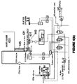
- FIG. 4( a ) is a simplified cross-sectional view of an apparatus for a lithography process for fabricating integrated circuits according an embodiment of the present invention.
- FIG. 4( b ) is a simplified schematic view of the apparatus of FIG. 4( a ).
- a semiconductor substrate is disposed on a chuck 403 .
- a photoresist material is deposited on the surface of the semiconductor substrate.
- a fiber optic waveguide 405 to direct light from light source 420 for exposing the photoresist material in predetermined area on the semiconductor substrate.
- the predetermined area is a wafer edge expose area.
- a lens 421 to expose the wafer to light is provided at an end of the fiber optic. The lens is positioned at a predetermined distance from the semiconductor wafer. The distance measures 0.5 ⁇ 0.2 mm in a specific embodiment.
- the apparatus includes a shutter 409 to allow exposure of the photoresist material.
- the shutter is controlled by a solenoid valve 411 .
- the apparatus also includes an air-spring valve 415 coupled to a gas source 417 .
- the air-spring valve controls a flow of the purging gas to flow through enclosure 407 .
- the purging gas can be compressed air in a specific embodiment.
- Other examples of purging gas gases includes nitrogen or an inert gas.
- the apparatus also includes a three way valve 413 , coupled in common with air-spring valve 415 and solenoid valve 411 .
- the three way valve opens and triggers solenoid valve 411 to open shutter 409 thereby exposing photoresist material on the semiconductor substrate.
- the three way valve triggers air spring valve 415 to open, allowing the purging gas to flow.
- the purging gas together with a vapor from the photoresist material during wafer edge expose process is removed using existing exhaust system on the tool. This prevents a solid to crystallize on the lens and eliminate steps of cleaning the lens.
- vapor may continue to be produced by the resist material even after the exposure step.
- optical elements of other types of tools including but not limited to the objective lenses of after develop inspection (ADI) tools or review optical microscope (OM) tools employed to inspect the exposed resist, may also be shielded from contamination by vapors utilizing alternative embodiments of the present invention.
Abstract
Description
Claims (10)
Applications Claiming Priority (3)
| Application Number | Priority Date | Filing Date | Title |
|---|---|---|---|
| CN200610024531.X | 2006-03-09 | ||
| CN200610024531XA CN101034261B (en) | 2006-03-09 | 2006-03-09 | Method and device for preventing barrier processing from polluting optical element |
| CN200610024531 | 2006-03-09 |
Publications (2)
| Publication Number | Publication Date |
|---|---|
| US20080106708A1 US20080106708A1 (en) | 2008-05-08 |
| US7701549B2 true US7701549B2 (en) | 2010-04-20 |
Family
ID=38730858
Family Applications (1)
| Application Number | Title | Priority Date | Filing Date |
|---|---|---|---|
| US11/512,662 Active 2028-11-16 US7701549B2 (en) | 2006-03-09 | 2006-08-29 | Method and apparatus to prevent contamination of optical element by resist processing |
Country Status (2)
| Country | Link |
|---|---|
| US (1) | US7701549B2 (en) |
| CN (1) | CN101034261B (en) |
Families Citing this family (4)
| Publication number | Priority date | Publication date | Assignee | Title |
|---|---|---|---|---|
| KR101399303B1 (en) | 2008-12-05 | 2014-05-26 | 엘지디스플레이 주식회사 | Exposing apparatus for flat panel display device |
| WO2015124344A1 (en) * | 2014-02-20 | 2015-08-27 | Asml Netherlands B.V. | Lithographic apparatus and device manufacturing method |
| CN107783283B (en) * | 2016-08-30 | 2020-01-24 | 上海微电子装备(集团)股份有限公司 | Lens anti-pollution device and method |
| CN111856887B (en) * | 2020-06-15 | 2022-10-14 | 上海集成电路研发中心有限公司 | Device for replacing dynamic gas lock on line |
Citations (9)
| Publication number | Priority date | Publication date | Assignee | Title |
|---|---|---|---|---|
| US4583840A (en) * | 1982-11-29 | 1986-04-22 | Canon Kabushiki Kaisha | Exposure apparatus |
| US5097136A (en) * | 1990-05-29 | 1992-03-17 | Ultra-Lum, Inc. | Apparatus for curing photosensitive coatings |
| JPH11111587A (en) * | 1997-09-30 | 1999-04-23 | Canon Inc | Projection aligner for manufacturing semiconductor and semiconductor device manufacture process using it |
| US20020000519A1 (en) * | 2000-04-14 | 2002-01-03 | Masami Tsukamoto | Contamination prevention in optical system |
| US6542220B1 (en) * | 1999-11-05 | 2003-04-01 | Asml Netherlands, B.V. | Purge gas systems for use in lithographic projection apparatus |
| US6721031B2 (en) * | 2001-06-15 | 2004-04-13 | Canon Kabushiki Kaisha | Exposure apparatus |
| US20040233401A1 (en) * | 2003-02-24 | 2004-11-25 | Naoki Irie | Exposure apparatus |
| US20050036121A1 (en) * | 2002-11-12 | 2005-02-17 | Asml Netherlands B.V. | Lithographic apparatus and device manufacturing method |
| US20050122493A1 (en) * | 2003-12-03 | 2005-06-09 | Canon Kabushiki Kaisha | Inert-gas purge method, exposure apparatus, device fabrication method and devices |
-
2006
- 2006-03-09 CN CN200610024531XA patent/CN101034261B/en not_active Expired - Fee Related
- 2006-08-29 US US11/512,662 patent/US7701549B2/en active Active
Patent Citations (9)
| Publication number | Priority date | Publication date | Assignee | Title |
|---|---|---|---|---|
| US4583840A (en) * | 1982-11-29 | 1986-04-22 | Canon Kabushiki Kaisha | Exposure apparatus |
| US5097136A (en) * | 1990-05-29 | 1992-03-17 | Ultra-Lum, Inc. | Apparatus for curing photosensitive coatings |
| JPH11111587A (en) * | 1997-09-30 | 1999-04-23 | Canon Inc | Projection aligner for manufacturing semiconductor and semiconductor device manufacture process using it |
| US6542220B1 (en) * | 1999-11-05 | 2003-04-01 | Asml Netherlands, B.V. | Purge gas systems for use in lithographic projection apparatus |
| US20020000519A1 (en) * | 2000-04-14 | 2002-01-03 | Masami Tsukamoto | Contamination prevention in optical system |
| US6721031B2 (en) * | 2001-06-15 | 2004-04-13 | Canon Kabushiki Kaisha | Exposure apparatus |
| US20050036121A1 (en) * | 2002-11-12 | 2005-02-17 | Asml Netherlands B.V. | Lithographic apparatus and device manufacturing method |
| US20040233401A1 (en) * | 2003-02-24 | 2004-11-25 | Naoki Irie | Exposure apparatus |
| US20050122493A1 (en) * | 2003-12-03 | 2005-06-09 | Canon Kabushiki Kaisha | Inert-gas purge method, exposure apparatus, device fabrication method and devices |
Non-Patent Citations (1)
| Title |
|---|
| Machine translation of JP H11-111587. * |
Also Published As
| Publication number | Publication date |
|---|---|
| CN101034261A (en) | 2007-09-12 |
| CN101034261B (en) | 2010-08-11 |
| US20080106708A1 (en) | 2008-05-08 |
Similar Documents
| Publication | Publication Date | Title |
|---|---|---|
| US6734443B2 (en) | Apparatus and method for removing photomask contamination and controlling electrostatic discharge | |
| US10739671B2 (en) | Method of manufacturing phase shift photo masks | |
| US7455880B2 (en) | Optical element fabrication method, optical element, exposure apparatus, device fabrication method | |
| US8142959B2 (en) | Method and apparatus for gating photomask contamination | |
| US7666576B2 (en) | Exposure scan and step direction optimization | |
| US7701549B2 (en) | Method and apparatus to prevent contamination of optical element by resist processing | |
| US7379151B2 (en) | Exposure apparatus comprising cleaning apparatus for cleaning mask with laser beam | |
| JP2002122980A (en) | Method for manufacturing semiconductor integrated circuit device and method for manufacturing photo mask | |
| JP3715189B2 (en) | Phase shift mask | |
| JP2005244015A (en) | Aligner, optical cleaning method of optical element in aligner, and process for fabricating device having fine pattern | |
| US9057955B2 (en) | Functional film, liquid immersion member, method of manufacturing liquid immersion member, exposure apparatus, and device manufacturing method | |
| US20040239900A1 (en) | Self-cleaning method for semiconductor exposure apparatus | |
| JP2004006690A (en) | Lithograph device and device manufacturing method | |
| JPH08227851A (en) | Method of photolithography and photolithography system for use therein | |
| US6280646B1 (en) | Use of a chemically active reticle carrier for photomask etching | |
| US9298085B2 (en) | Method for repairing a mask | |
| US9535317B2 (en) | Treating a capping layer of a mask | |
| US20050109278A1 (en) | Method to locally protect extreme ultraviolet multilayer blanks used for lithography | |
| US7463336B2 (en) | Device manufacturing method and apparatus with applied electric field | |
| US9897910B2 (en) | Treating a capping layer of a mask | |
| US7008730B2 (en) | Application of high transmittance attenuating phase shifting mask with dark tone for sub-0.1 micrometer logic device contact hole pattern in 193 NM lithography | |
| US20070177117A1 (en) | Exposure apparatus and device manufacturing method | |
| KR100236712B1 (en) | Illumination of semiconductor stepper | |
| US20060236921A1 (en) | Method of cleaning a substrate surface from a crystal nucleus | |
| KR20220141898A (en) | Conduit system, radiation source, lithographic apparatus and method thereof |
Legal Events
| Date | Code | Title | Description |
|---|---|---|---|
| AS | Assignment |
Owner name: SEMICONDUCTOR MANUFACTURING INTERNATIONAL (SHANGHA Free format text: ASSIGNMENT OF ASSIGNORS INTEREST;ASSIGNORS:CHEN, CHIN YU;LAM, SAI HUNG;TANG, ZHENG LONG;SIGNING DATES FROM 20070601 TO 20070702;REEL/FRAME:024024/0695 |
|
| AS | Assignment |
Owner name: SEMICONDUCTOR MANUFACTURING INTERNATIONAL (SHANGHA Free format text: ASSIGNMENT OF ASSIGNORS INTEREST;ASSIGNOR:CHANG, HSU SHENG;REEL/FRAME:024032/0322 Effective date: 20010802 |
|
| STCF | Information on status: patent grant |
Free format text: PATENTED CASE |
|
| FPAY | Fee payment |
Year of fee payment: 4 |
|
| MAFP | Maintenance fee payment |
Free format text: PAYMENT OF MAINTENANCE FEE, 8TH YEAR, LARGE ENTITY (ORIGINAL EVENT CODE: M1552) Year of fee payment: 8 |
|
| MAFP | Maintenance fee payment |
Free format text: PAYMENT OF MAINTENANCE FEE, 12TH YEAR, LARGE ENTITY (ORIGINAL EVENT CODE: M1553); ENTITY STATUS OF PATENT OWNER: LARGE ENTITY Year of fee payment: 12 |