US7710092B2 - Self tracking ADC for digital power supply control systems - Google Patents
Self tracking ADC for digital power supply control systems Download PDFInfo
- Publication number
- US7710092B2 US7710092B2 US11/876,756 US87675607A US7710092B2 US 7710092 B2 US7710092 B2 US 7710092B2 US 87675607 A US87675607 A US 87675607A US 7710092 B2 US7710092 B2 US 7710092B2
- Authority
- US
- United States
- Prior art keywords
- digital
- power supply
- adc
- output
- voltage
- Prior art date
- Legal status (The legal status is an assumption and is not a legal conclusion. Google has not performed a legal analysis and makes no representation as to the accuracy of the status listed.)
- Expired - Lifetime, expires
Links
- 230000004044 response Effects 0.000 claims abstract description 10
- 238000012937 correction Methods 0.000 claims abstract description 6
- 238000012546 transfer Methods 0.000 claims description 17
- 238000005259 measurement Methods 0.000 claims description 7
- 230000002093 peripheral effect Effects 0.000 claims description 4
- 230000014509 gene expression Effects 0.000 claims description 3
- 230000033228 biological regulation Effects 0.000 description 7
- 238000000034 method Methods 0.000 description 5
- 230000010355 oscillation Effects 0.000 description 5
- 230000008901 benefit Effects 0.000 description 4
- 239000003990 capacitor Substances 0.000 description 4
- 230000008859 change Effects 0.000 description 4
- 238000013507 mapping Methods 0.000 description 4
- 238000006243 chemical reaction Methods 0.000 description 3
- 230000007423 decrease Effects 0.000 description 3
- 238000010586 diagram Methods 0.000 description 3
- 238000012544 monitoring process Methods 0.000 description 3
- 230000001105 regulatory effect Effects 0.000 description 3
- 230000001276 controlling effect Effects 0.000 description 2
- 238000013139 quantization Methods 0.000 description 2
- 230000001052 transient effect Effects 0.000 description 2
- 230000006978 adaptation Effects 0.000 description 1
- 230000003044 adaptive effect Effects 0.000 description 1
- 238000011217 control strategy Methods 0.000 description 1
- 230000003247 decreasing effect Effects 0.000 description 1
- 230000003111 delayed effect Effects 0.000 description 1
- 230000001419 dependent effect Effects 0.000 description 1
- 230000009977 dual effect Effects 0.000 description 1
- 230000000694 effects Effects 0.000 description 1
- 238000012986 modification Methods 0.000 description 1
- 230000004048 modification Effects 0.000 description 1
- 230000008569 process Effects 0.000 description 1
- 238000011084 recovery Methods 0.000 description 1
- 230000009467 reduction Effects 0.000 description 1
- 230000004043 responsiveness Effects 0.000 description 1
- 238000005096 rolling process Methods 0.000 description 1
- 230000003068 static effect Effects 0.000 description 1
- 239000002699 waste material Substances 0.000 description 1
Images


Classifications
-
- H—ELECTRICITY
- H02—GENERATION; CONVERSION OR DISTRIBUTION OF ELECTRIC POWER
- H02M—APPARATUS FOR CONVERSION BETWEEN AC AND AC, BETWEEN AC AND DC, OR BETWEEN DC AND DC, AND FOR USE WITH MAINS OR SIMILAR POWER SUPPLY SYSTEMS; CONVERSION OF DC OR AC INPUT POWER INTO SURGE OUTPUT POWER; CONTROL OR REGULATION THEREOF
- H02M3/00—Conversion of dc power input into dc power output
- H02M3/02—Conversion of dc power input into dc power output without intermediate conversion into ac
- H02M3/04—Conversion of dc power input into dc power output without intermediate conversion into ac by static converters
- H02M3/10—Conversion of dc power input into dc power output without intermediate conversion into ac by static converters using discharge tubes with control electrode or semiconductor devices with control electrode
- H02M3/145—Conversion of dc power input into dc power output without intermediate conversion into ac by static converters using discharge tubes with control electrode or semiconductor devices with control electrode using devices of a triode or transistor type requiring continuous application of a control signal
- H02M3/155—Conversion of dc power input into dc power output without intermediate conversion into ac by static converters using discharge tubes with control electrode or semiconductor devices with control electrode using devices of a triode or transistor type requiring continuous application of a control signal using semiconductor devices only
- H02M3/156—Conversion of dc power input into dc power output without intermediate conversion into ac by static converters using discharge tubes with control electrode or semiconductor devices with control electrode using devices of a triode or transistor type requiring continuous application of a control signal using semiconductor devices only with automatic control of output voltage or current, e.g. switching regulators
- H02M3/158—Conversion of dc power input into dc power output without intermediate conversion into ac by static converters using discharge tubes with control electrode or semiconductor devices with control electrode using devices of a triode or transistor type requiring continuous application of a control signal using semiconductor devices only with automatic control of output voltage or current, e.g. switching regulators including plural semiconductor devices as final control devices for a single load
- H02M3/1588—Conversion of dc power input into dc power output without intermediate conversion into ac by static converters using discharge tubes with control electrode or semiconductor devices with control electrode using devices of a triode or transistor type requiring continuous application of a control signal using semiconductor devices only with automatic control of output voltage or current, e.g. switching regulators including plural semiconductor devices as final control devices for a single load comprising at least one synchronous rectifier element
-
- H—ELECTRICITY
- H02—GENERATION; CONVERSION OR DISTRIBUTION OF ELECTRIC POWER
- H02M—APPARATUS FOR CONVERSION BETWEEN AC AND AC, BETWEEN AC AND DC, OR BETWEEN DC AND DC, AND FOR USE WITH MAINS OR SIMILAR POWER SUPPLY SYSTEMS; CONVERSION OF DC OR AC INPUT POWER INTO SURGE OUTPUT POWER; CONTROL OR REGULATION THEREOF
- H02M3/00—Conversion of dc power input into dc power output
- H02M3/02—Conversion of dc power input into dc power output without intermediate conversion into ac
- H02M3/04—Conversion of dc power input into dc power output without intermediate conversion into ac by static converters
- H02M3/10—Conversion of dc power input into dc power output without intermediate conversion into ac by static converters using discharge tubes with control electrode or semiconductor devices with control electrode
- H02M3/145—Conversion of dc power input into dc power output without intermediate conversion into ac by static converters using discharge tubes with control electrode or semiconductor devices with control electrode using devices of a triode or transistor type requiring continuous application of a control signal
- H02M3/155—Conversion of dc power input into dc power output without intermediate conversion into ac by static converters using discharge tubes with control electrode or semiconductor devices with control electrode using devices of a triode or transistor type requiring continuous application of a control signal using semiconductor devices only
- H02M3/156—Conversion of dc power input into dc power output without intermediate conversion into ac by static converters using discharge tubes with control electrode or semiconductor devices with control electrode using devices of a triode or transistor type requiring continuous application of a control signal using semiconductor devices only with automatic control of output voltage or current, e.g. switching regulators
- H02M3/157—Conversion of dc power input into dc power output without intermediate conversion into ac by static converters using discharge tubes with control electrode or semiconductor devices with control electrode using devices of a triode or transistor type requiring continuous application of a control signal using semiconductor devices only with automatic control of output voltage or current, e.g. switching regulators with digital control
-
- H—ELECTRICITY
- H03—ELECTRONIC CIRCUITRY
- H03M—CODING; DECODING; CODE CONVERSION IN GENERAL
- H03M1/00—Analogue/digital conversion; Digital/analogue conversion
- H03M1/12—Analogue/digital converters
- H03M1/48—Servo-type converters
-
- Y—GENERAL TAGGING OF NEW TECHNOLOGICAL DEVELOPMENTS; GENERAL TAGGING OF CROSS-SECTIONAL TECHNOLOGIES SPANNING OVER SEVERAL SECTIONS OF THE IPC; TECHNICAL SUBJECTS COVERED BY FORMER USPC CROSS-REFERENCE ART COLLECTIONS [XRACs] AND DIGESTS
- Y02—TECHNOLOGIES OR APPLICATIONS FOR MITIGATION OR ADAPTATION AGAINST CLIMATE CHANGE
- Y02B—CLIMATE CHANGE MITIGATION TECHNOLOGIES RELATED TO BUILDINGS, e.g. HOUSING, HOUSE APPLIANCES OR RELATED END-USER APPLICATIONS
- Y02B70/00—Technologies for an efficient end-user side electric power management and consumption
- Y02B70/10—Technologies improving the efficiency by using switched-mode power supplies [SMPS], i.e. efficient power electronics conversion e.g. power factor correction or reduction of losses in power supplies or efficient standby modes
Definitions
- the present invention relates to power supply circuits, and more particularly to digital control systems and methods for switched mode power supply circuits.
- Switched mode power supplies are known in the art to convert an available direct current (DC) or alternating current (AC) level voltage to another DC level voltage.
- a buck converter is one particular type of switched mode power supply that provides a regulated DC output voltage to a load by selectively storing energy in an output inductor coupled to the load by switching the flow of current into the output inductor. It includes two power switches that are typically provided by MOSFET transistors.
- a filter capacitor coupled in parallel with the load reduces ripple of the output current.
- a pulse width modulation (PWM) control circuit is used to control the gating of the power switches in an alternating manner to control the flow of current in the output inductor.
- the PWM control circuit uses signals communicated via a feedback loop reflecting the output voltage and/or current level to adjust the duty cycle applied to the power switches in response to changing load conditions.
- a conventional digital control circuit includes an analog-to-digital converter (ADC) that converts an error signal representing the difference between a signal to be controlled (e.g., output voltage (V o )) and a reference into a digital signal having n bits.
- ADC analog-to-digital converter
- the digital control circuit uses the digital error signal to control a digital pulse width modulator, which provides control signals to the power switches having a duty cycle such that the output value of the power supply tracks the reference.
- a digital pulse width modulator which provides control signals to the power switches having a duty cycle such that the output value of the power supply tracks the reference.
- the number of bits of the digital signal needs to be sufficiently high to provide resolution good enough to secure precise control of the output value.
- the ADC needs to be very fast to respond to changing load conditions.
- Current microprocessors exhibit supply current slew rates of up to 20 A/ ⁇ s, and future microprocessors are expected to reach slew rates greater than 350 A/ ⁇ s, thereby demanding extremely fast response by the power supply.
- Single stage (i.e., flash) ADC topologies are utilized in power supply control circuit applications since they have very low latency (i.e., overall delay between input and output for a particular sample). If a standard flash ADC device is used to quantize the full range of regulator output voltage with desired resolution (e.g., 5 mV), the device will necessarily require a large number of comparators that will dissipate an undesirable amount of power. Under normal operation, the output voltage V o of the regulator remains within a small window, which means that the ADC need not have a high resolution over the entire range. Accordingly, a “windowed” ADC topology permits high resolution over a relatively small voltage range tracked by a reference voltage (V ref ).
- V ref reference voltage
- the windowed ADC provides the dual functions of the ADC and error amplifier, resulting in a further reduction of components and associated power dissipation.
- a drawback with the windowed ADC topology is that the device can go into saturation due to transient load conditions that cause the window ranges to be exceeded.
- a 4-bit windowed ADC has a least significant bit (LSB) resolution of roughly 5 mV. This means that an output voltage error of as low as ⁇ 40 mV pushes the ADC into saturation.
- the ADC would then continue to reflect the same error signal (i.e., maximum) even though the actual error could grow even larger, referred to as a “windup” condition of the digital control system.
- the reaction of the feedback loop in this windup condition can be difficult to predict, since without accurate information about the error size the digital control system no longer functions as a linear system. This behavior can be particularly harmful, since it can damage the load due to overcurrent and/or overvoltage, and can also damage the power supply itself.
- ADC Analog to digital converter
- ADC circuit that provides a digital representation of a parameter that needs to be regulated (e.g., the absolute output voltage of a power supply), so that any additional monitoring and supervisory circuits could be implemented as full digital circuits. Furthermore, it would be advantageous to provide an ADC circuit having high resolution around the steady state operating point of the power supply, but that can also settle quickly to a new operating point.
- the present invention provides a self-tracking analog-to-digital converter (ADC) for use in applications such as in a switched mode power supply.
- ADC analog-to-digital converter
- the self-tracking ADC overcomes the disadvantages of the prior art by providing a digital representation of a parameter under regulation (e.g., the absolute output voltage of a power supply), thereby enabling any additional monitoring and supervisory circuits to be implemented as full digital circuits.
- a self-tracking analog-to-digital converter includes a digital-to-analog converter (DAC) adapted to provide a variable reference voltage, a windowed flash analog-to-digital converter (ADC) adapted to provide an error signal e k corresponding to a difference between an input voltage V i and the variable reference voltage, and digital circuitry adapted to generate suitable control signals for the DAC based on the error signal e k .
- the digital circuitry includes a first digital circuit adapted to provide a first function value f(e k ) in response to the error signal e k , the first function value f(e k ) representing an amount of correction to be applied to the variable reference voltage.
- a second digital circuit is adapted to provide a counter that combines the first function value f(e k ) with a previous counter state N k to provide a next counter state N k+1 , the next counter state N k+1 being applied as an input to the digital-to-analog converter.
- a third digital circuit is adapted to scale the previous counter state N k by a factor M and combine the scaled counter state M ⁇ N k with the error signal e k to provide a digital output value D k representing the input voltage V i .
- a switched mode power supply comprises at least one power switch adapted to convey power between input and output terminals of the power supply, and a digital controller adapted to control operation of the at least one power switch responsive to an output measurement of the power supply.
- the digital controller includes the self-tracking analog-to-digital converter, a digital filter providing a digital control output based on a difference between a digital output of the self-tracking analog-to-digital converter and a reference value, and a digital pulse width modulator providing a control signal to the at least one power switch.
- the self-tracking analog to digital converter comprises a digital-to-analog converter (DAC) adapted to provide a variable reference voltage, a windowed flash analog-to-digital converter (ADC) adapted to provide an error signal e k corresponding to a difference between the output measurement and the variable reference voltage, a first digital circuit adapted to generate a first function value f(e k ) in response to the error signal e k , the first function value f(e k ) representing an amount of correction to be applied to the variable reference voltage, a second digital circuit adapted to provide a counter that combines the first function value f(e k ) with a previous counter state N k to provide a next counter state N k+1 , the next counter state N k+1 being applied as an input to the DAC, and a third digital circuit adapted to scale the previous counter state N k by a factor M and combine the scaled counter state M ⁇ N k with the error signal e k to provide a digital output value D
- FIG. 1 depicts a switched mode power supply having a digital control circuit
- FIG. 2 depicts a windowed flash ADC that provides high and low saturation signals
- FIG. 3 depicts a digital controller having an infinite impulse response filter and error controller
- FIG. 4 is a graph depicting a linear ADC transfer function
- FIG. 5 is a graph depicting a linear ADC transfer function with an increased step size at the window boundaries in accordance with an embodiment of the invention
- FIG. 6 is a graph depicting a non-linear ADC transfer function with increased step size and increased gain at the window boundaries in accordance with another embodiment of the invention.
- FIG. 7 is a block diagram of a self-tracking ADC in accordance with an embodiment of the invention.
- FIG. 8 graphically illustrates a range of exemplary comparator thresholds for the self-tracking ADC of FIG. 7 ;
- FIG. 9 is a block diagram of a self-tracking ADC in accordance with another embodiment of the invention.
- FIG. 10 graphically illustrates a range of exemplary comparator thresholds for the self-tracking ADC of FIG. 9 ;
- FIG. 11 graphically illustrates a range of exemplary comparator thresholds for an alternative embodiment of the self-tracking ADC that avoids limit cycle oscillations.
- FIG. 12 depicts a switched mode power supply having a digital control circuit that includes a self-tracking ADC.
- the present invention provides a method for digitally controlling a switched mode power supply. More specifically, the invention provides an ADC circuit that produces a digital representation of a parameter that needs to be regulated (e.g., the absolute output voltage of a power supply), so that any additional monitoring and supervisory circuits could be implemented as full digital circuits.
- a parameter that needs to be regulated e.g., the absolute output voltage of a power supply
- FIG. 1 depicts an exemplary switched mode power supply 10 having a digital control circuit in accordance with an embodiment of the present invention.
- the power supply 10 comprises a buck converter topology to convert an input DC voltage V in to an output DC voltage V o applied to a resistive load 20 (R load ).
- the power supply 10 includes a pair of power switches 12 , 14 provided by MOSFET devices. The drain terminal of the high side power switch 12 is coupled to the input voltage V in , the source terminal of the low side power switch 14 is connected to ground, and the source terminal of the power switches 12 is coupled to the drain terminal of the power switch 14 to define a phase node.
- An output inductor 16 is coupled in series between the phase node and the terminal providing the output voltage V o , and a capacitor 18 is coupled in parallel with the resistive load R load .
- Respective drivers 22 , 24 alternatingly drive the gate terminals of the power switches 12 , 14 .
- the drivers 22 , 24 are controlled by digital control circuit 30 (described below).
- the opening and closing of the power switches 12 , 14 provides an intermediate voltage having a generally rectangular waveform at the phase node, and the filter formed by the output inductor 16 and capacitor 18 converts the rectangular waveform into a substantially DC output voltage V o .
- the digital control circuit 30 receives a feedback signal from the output portion of the power supply 10 .
- the feedback signal corresponds to the output voltage V o , though it should be appreciated that the feedback signal could alternatively (or additionally) correspond to the output current drawn by the resistive load R load or any other signal representing a parameter to be controlled by the digital control circuit 30 .
- the feedback path may further include a voltage divider (not shown) to reduce the detected output voltage V o to a representative voltage level.
- the digital control circuit 30 provides a pulse width modulated waveform having a duty cycle controlled to regulate the output voltage V o (or output current) at a desired level.
- the exemplary power supply 10 is illustrated as having a buck converter topology, it should be understood that the use of feedback loop control of the power supply 10 using the digital control circuit 30 is equally applicable to other known power supply topologies, such as boost and buck-boost converters in both isolated and non-isolated configurations, and to different control strategies known as voltage mode, current mode, charge mode and/or average current mode controllers.
- the digital control circuit 30 includes analog-to-digital converter (ADC) 32 , digital controller (G(z)) 34 , and digital pulse width modulator (DPWM) 36 .
- the ADC 32 further comprises a windowed flash ADC that receives as inputs the feedback signal (i.e., output voltage V o ) and a voltage reference (Ref) and produces a digital voltage error signal (VEd k ) representing the difference between the inputs (Ref ⁇ V o ).
- the feedback signal i.e., output voltage V o
- Ref voltage reference
- VEd k digital voltage error signal
- the digital controller 34 has a transfer function G(z) that transforms the voltage error signal VEd k to a digital output provided to the DPWM 36 , which converts the signal into a waveform having a proportional pulse width (PWM k ).
- PWM k proportional pulse width
- the pulse-modulated waveform PWM k produced by the DPWM 36 is coupled to the gate terminals of the power switches 12 , 14 through the respective drivers 22 , 24 .
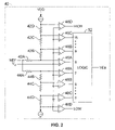
- FIG. 2 depicts an exemplary windowed flash ADC 40 for use in the digital control circuit 30 .
- the ADC 40 receives as inputs the voltage reference Ref and the output voltage V o .
- the voltage reference is applied to the center of a resistor ladder that includes resistors 42 A, 42 B, 42 C, 42 D connected in series between the reference voltage terminal and a current source connected to a positive supply voltage (V DD ), and resistors 44 A, 44 B, 44 C, 44 D connected in series between the reference voltage terminal and a current source connected to ground.
- the resistors each have corresponding resistance values to define together with the current sources a plurality of voltage increments ranging above and below the voltage reference Ref.
- the magnitude of the resistance values and/or current sources can be selected to define the LSB resolution of the ADC 40 .
- An array of comparators is connected to the resistor ladder, including a plurality of positive side comparators 46 A, 46 B, 46 C, 46 D and a plurality of negative side comparators 48 A, 48 B, 48 C, 48 D.
- the positive side comparators 46 A, 46 B, 46 C, 46 D each have a non-inverting input terminal connected to the output voltage V o , and an inverting input terminal connected to respective ones of the resistors 42 A, 42 B, 42 C, 42 D.
- the negative side comparators 48 A, 48 B, 48 C each have a non-inverting input terminal connected to the output voltage V o , and an inverting input terminal connected to respective ones of the resistors 44 A, 44 B, 44 C, 44 D.
- Negative side comparator 48 D has a non-inverting input terminal connected to ground and the inverting input terminal connected to the output voltage V o . It should be appreciated that a greater number of resistors and comparators may be included to increase the number of voltage increments and hence the range of the ADC 40 , and that a limited number of resistors and comparators is shown in FIG. 2 for exemplary purposes only.
- the ADC 40 further includes a logic device 52 coupled to output terminals of comparators 46 A, 46 B, 46 C and 48 A, 48 B, 48 C.
- the logic device 52 receives the comparator outputs and provides a multi-bit (e.g., 4-bit) parallel output representing the digital voltage error VEd k .
- a multi-bit e.g., 4-bit
- an output voltage V o that exceeds the reference voltage Ref by one and a half voltage increments would cause the outputs of comparators 46 B, 46 A, 48 A, 48 B, and 48 C to go high, while the outputs of comparators 46 C, 46 D and 48 D remain low.
- the logic device 52 would interpret this as logic level 9 (or binary 1001 ) and produce an associated voltage error signal VEd k .
- the voltage reference Ref is variable so as to shift the window of the ADC 40 . If the output voltage V o exceeds the highest voltage increment of the resistor ladder, the output terminal of comparator 46 D provides a HIGH saturation signal. Similarly, if the output voltage V o is lower than the lowest voltage increment of the resistor ladder, the output terminal of comparator 48 D provides a LOW saturation signal.
- the resistors 44 A, 44 B, 44 C, 44 D have equal values so as to define a plurality of n voltage references equally spaced above and below the reference voltage Ref.
- the n comparators 46 A, 46 B, 46 C and 48 A, 48 B, 48 C compare the actual output voltage V O against the n voltage references and generate a corresponding “thermometer” code, such that comparators 0 to X have an output of one and comparators X+1 to n have an output of zero, with X depending on the voltage amplitude of the V O signal.
- the range that the windowed flash ADC 40 is able to convert into a digital signal is limited by the step size between each reference voltage and the number of comparators.
- an exemplary implementation may include sixteen comparators.
- the step size of the circuit should be kept low enough (e.g., 5 mV) by selecting appropriate values of the resistors to provide enough resolution in the feedback loop.
- the step size directly relates to the output voltage static regulation and also the noise added to the output voltage due to the quantization of the error signal. With sixteen comparators and a 5 mV step size, the overall window is only ⁇ 40 mV.
- the dynamic voltage excursion can easily exceed 40 mV.
- the ADC 40 saturates and the voltage error signal VEd k is no longer linear, i.e., it is not proportional to the actual error.
- the output terminal of comparator 46 D provides a HIGH saturation signal to reflect this saturation condition.
- FIG. 4 illustrates a graph depicting a linear ADC transfer function in accordance with a conventional windowed flash ADC.
- the horizontal dimension of the graph reflects the analog error signals input to the logic device 52 and the vertical dimension reflects the digital output from the logic device.
- the practical window size of the ADC is fairly limited, which has certain disadvantages. Namely, it makes the feedback system non-linear during large and sudden load changes, which tends to make it difficult to guarantee stability in such conditions.
- the circuit can become unstable and produce a limit cycle oscillation between the ADC window boundaries.
- FIG. 5 illustrates a graph depicting an ADC transfer function in which the step size is changed in accordance with an embodiment of the invention.
- the horizontal dimension of the graph reflects the analog error signals input to the logic device 52 and the vertical dimension reflects the digital output of the logic device.
- the step size is increased in the region adjacent to the boundary of the ADC window by using different resistor values in the boundary regions.
- the logic device 52 is changed such that the “temperature” code out of the comparators is mapped into a digital number matching the increased step size at the boundary of the window. This keeps the overall transfer function of the ADC linear. While the window is enlarged overall, the gain is substantially unaffected.
- the decreased resolution at the ADC boundary regions is acceptable since the steady state voltage of the ADC will always be around zero error (assuming a controller transfer function with a pole at zero). At zero error, the resolution is the same as with the previous embodiment and therefore stability and output voltage precision is unaffected.
- the larger step size of the ADC only affects the circuit during large dynamic changes, i.e., step increases or decreases in load current). Since this is a dynamic process, the precision of the regulation is not important, but by providing a gain number proportional to the actual error the overall stability of the circuit is improved.
- FIG. 5 illustrates the use of two different step sizes, i.e., a first step size in the center of the ADC window and a second, larger step size in the peripheral region of the window. It should be appreciated that there may alternatively be a plurality of intermediary gradations of step size ranging from the first step size in the center of the ADC window to the second step size at the periphery. Each of these gradations of step size would nevertheless be mapped into digital numbers matching the corresponding step size to keep the overall transfer function of the ADC linear.
- the ADC transfer function of FIG. 5 increases the ADC window size to improve stability robustness and provides a linear relationship between ADC input and output over a larger window size, it does not provide faster settling time during transient regulation conditions.
- the transfer function is further modified to increase the step size at the window boundary as in the preceding embodiment, and also the transfer function is made non-linear toward the window boundary so that the error reported to the controller 36 is larger than the actual value.
- the step size and mapping to the digital number is as in the preceding embodiments. But, at the peripheral region of the window, the magnitude of the digital output is increased out of proportion with the step increases of the analog input.
- the non-linear mapping in the peripheral region of the window helps to speed up the feedback loop for large dynamic errors without altering the small signal stability in steady state conditions.
- the horizontal dimension of the graph reflects the analog error input to the logic circuit 52 and the vertical dimension reflects the digital output of the logic circuit. It should be appreciated that there may be a plurality of gradations of step size and mapping to the digital numbers at the periphery of the ADC window.
- the digital filter further comprises an infinite impulse response (IIR) filter that produces an output PWM′ k from previous voltage error inputs VEd k and previous outputs PWM′ k .
- IIR infinite impulse response
- ADC 40 provides the voltage error inputs VEd k .
- the digital filter outputs PWM′ k are provided to the digital pulse width modulator (DPWM) 36 , which provides the pulse width modulated control signal (PWM k ) to the power supply power switches.
- DPWM digital pulse width modulator
- the IIR filter is illustrated in block diagram form and includes a first plurality of delay registers 72 , 74 , . . . , 76 (each labeled z ⁇ 1 ), a first plurality of mathematical operators (multipliers) with coefficients 71 , 73 , . . . , 77 (labeled C 0 , C 1 , . . . , Cn), a second plurality of mathematical operators (adders) 92 , 94 , 96 , a second plurality of delay registers 82 , 84 , . . .
- each of the first delay registers 72 , 74 , 76 holds a previous sample of the voltage error VEd k , which is then weighted by a respective one of the coefficients 71 , 73 , 77 .
- each of the second delay registers 82 , 84 , 86 holds a previous sample of the output PWM′ k , which is then weighted by a respective one of the coefficients 83 , 87 .
- the adders 92 , 94 , and 96 combine the weighted input and output samples. It should be appreciated that a greater number of delay registers and coefficients may be included in the IIR filter, and that a limited number is shown in FIG. 3 for exemplary purposes only.
- the digital filter structure shown in FIG. 3 is an exemplary implementation of the following transfer function G(z):
- the error controller 62 receives a plurality of input signals reflecting error conditions of the ADC 40 and the digital filter. Specifically, the error controller 62 receives the HIGH and LOW saturation signals from the ADC 40 reflecting that the output voltage V o is above and below the voltage window of the ADC, respectively.
- Each of the mathematical operators (adders) 92 , 94 , 96 provides an overflow signal to the error controller 62 reflecting an overflow condition (i.e., carry bit) of the mathematical operators.
- the digital filter further includes a range limiter 81 that clips the output PWM′ k if upper or lower range limits are reached. In that situation, the range limiter 81 provides the error controller 62 with a corresponding limit signal.
- the error controller 62 uses these input signals to alter the operation of the digital filter in order to improve the responsiveness of the digital filter to changing load conditions.
- the error controller 62 is coupled to each of the first plurality of delay registers 72 , 74 , 76 and second plurality of delay registers 82 , 84 , 86 to enable the resetting and/or presetting of the value stored therein.
- resetting refers to the setting of the value to an initial value (e.g., zero)
- presetting refers to the setting of the value to another predetermined number.
- the error controller 62 can replace the previous samples of the voltage error VEd k and output PWM′ k with predetermined values that change the behavior of the power supply.
- the digital controller further includes multiplexer 64 that enables selection between the PWM′ k output signal and a predetermined output signal provided by the error controller 62 .
- a select signal provided by the error controller 62 determines which signal passes through the multiplexer 64 .
- the error controller 62 sets the PWM′ k signal to a specific predetermined value (or sequence of values that are dependent in part on the previous samples) by controlling the multiplexer 64 .
- the error controller can also alter the delayed input and output samples by reloading the first plurality of delay registers 72 , 74 , 76 , and second plurality of delay registers 82 , 84 , 86 . This will assure a controlled behavior of the feedback loop as the ADC 40 recovers from saturation.
- the PWM′ k sample can be reset to zero to help to reduce the error.
- the pulse width delivered to the high side power switch 12 of the power supply 10 goes to zero, effectively shutting off power to the resistive load 20 (see FIG. 1 ).
- the samples PWM′ k ⁇ 1 , PWM′ k ⁇ 2 , . . . , PWM′ k ⁇ n can also be reset to zero or preset to another value in order to allow a smooth recovery.
- the PWM′ k sample can be preset to a maximum value to increase the pulse width delivered to the high side power switch 12 to reduce the error.
- the error controller 62 can take actions to prevent uncontrolled command of the power switches of the power supply, such as altering the input and output samples of the digital filters.
- the ADC is configured to provide a digital representation of the absolute output voltage (V o ).
- V o the absolute output voltage
- This digital representation of the output voltage V o can then be further utilized by other power supply supervisory circuits to provide functions such as under-voltage protection, Power-Good-Low monitor, Power-Good-High monitor, and over-voltage protection.
- the entire control circuitry for the power supply can be implemented using digital circuitry, thereby eliminating the need for analog circuit components such as comparators.
- FIG. 7 illustrates an exemplary embodiment of a self-tracking ADC having an analog section 110 and a digital section 120 .
- the analog section 110 includes a windowed flash ADC 112 and a digital-to-analog converter (DAC) 114 .
- a subtractor 115 produces a voltage representing a difference between an input voltage (V i ) and a variable reference voltage generated by the DAC 114 .
- the windowed flash ADC 112 digitizes the voltage difference and provides an error signal e k to the digital section 120 , which corrects the DAC variable reference voltage so that it tracks the input voltage V i .
- the input voltage V i to the self-tracking ADC may actually be the output voltage V o of the power supply, as described above in the preceding embodiments.
- the input voltage V i may be any other voltage for which regulation is desired.
- the digital section 120 further includes a clamp 122 , an integrator 124 , an adder 125 , and a function circuit 128 that combine to generate the new digital reference N k that will be converted back into an analog voltage by DAC 114 .
- the error signal e k is further used to generate together with the reference value N k the absolute representation of the input voltage V i .
- the coarse input voltage V i representation is provided by N k
- a fine difference value between the coarse DAC reference N k and the real input voltage is provided by the value e k .
- the output e k of the flash windowed ADC 112 is applied to the function circuit 128 .
- the function circuit 128 generates a value f(e k ) that represents the correction to be applied to the variable reference voltage so that it tracks more closely the input voltage.
- the value f(e k ) is applied to a counter formed by integrator 124 , clamp 122 , and adder 125 .
- the adder 125 combines the value f(e k ) to the previous counter state N k and gets clamped by the clamp 122 .
- the clamp 122 provides an output corresponding to the next counter state N k+1 .
- the clamp 122 serves to limit the count value and prevent the counter from rolling over.
- the next state N k+1 of the counter is applied to the DAC 114 and gets sampled on the next clock cycle by the integrator 124 .
- the counter state N k is used together with the ADC error signal e k to determine the digital representation of the absolute input voltage V i .
- the counter state N k is scaled with the resolution difference M by multiplier 126 and the result is added to the ADC error e k by adder 127 .
- another clamp circuit 130 may be coupled to the output of adder 127 to avoid negative digital values or excessive high values.
- the output value D k represents the digital representation of the absolute input voltage V i .
- the resolution of DAC 114 as compared to the mid-band resolution of the windowed flash ADC 112 is lower by a constant factor M.
- ADC 112 could have a mid-band least significant bit (LSB) resolution of 5 mV.
- LSB resolution of DAC 114 would thus be 25 mV.
- the DAC 114 will therefore generate a relatively coarse reference voltage close to the input voltage, and the ADC 112 will generate an error e k compared to this coarse reference voltage.
- the windowed flash ADC 112 has also a much higher resolution in the middle of its window; in contrast, the resolution decreases towards the edge of the window.
- the DAC 114 could have a total of 8 bits (e.g., defining a range from 0 to 6.375V), the windowed flash ADC 112 could have a total of eighteen comparators with a mid-band resolution of 5 mV, and M could be equal to 5.
- the ADC 112 also will be able to track input signals changing with a rate of 7 ⁇ 25 mV per clock cycle.
- the values e k to be added to M ⁇ N k to produce the output D k can be relatively large, but only a few values out of the complete range will actually be used because of the coarse resolution of the window ADC 112 on its boundaries. This may represent a waste of resources for certain applications. Also, the ADC 112 may not produce directly the value e k , but more likely would produce a bit pattern corresponding to the comparator outputs.
- FIG. 9 illustrates a modified digital section 140 that includes a clamp 142 , an integrator 144 , and an adder 145 arranged as in FIG. 7 to provide a counter.
- the embodiment of FIG. 9 includes a look up table (LUT) 146 that provides a first function value f(e k ) to the adder 145 .
- the resulting digital reference N k+1 will be converted back into an analog voltage by DAC 114 .
- the LUT 146 also provides a second function value g(e k ) used to produce the digital representation of the absolute input voltage V i .
- the new counter state N k+1 is scaled with the resolution difference M by multiplier 148 and the result is added to the second function value g(e k ) by adder 147 .
- Another clamp circuit 150 may be coupled to the output of adder 17 to avoid negative digital values or excessive high values.
- the output value D k represents the digital representation of the absolute input voltage V i .
- the function g(e k ) can only take the values given by the following inequality: ⁇ M/ 2 ⁇ g ( e k ) ⁇ M/ 2 In the example above, g(e k ) would
- the switchpoints causing the DAC 114 to increment and decrement in mid-band should not be symmetric. This will introduce a small hysteresis and will eliminate the limit cycle oscillation. No change in thresholds are necessary to accomplish this. For example, a different encoding of the g(e k ) and f(e k ) values as shown in FIG. 11 will have the same effect. Note that changes to the preceding FIG. 10 are marked in grey in FIG. 11 . The hysteresis is graphically shown in FIG. 11 as an asymmetry between the +1 and ⁇ 1 values of f(e k ).
- FIG. 12 illustrates an exemplary switched mode power supply (as in FIG. 1 ) including a digital control circuit having the self-tracking ADC as discussed above with respect to FIGS. 7-11 .
- the digital control circuit includes a digital controller 34 and a digital pulse width modulator (DPWM) 36 .
- the digital control circuit further includes a self-tracking ADC comprising DAC 114 , adder 115 and flash windowed ADC 112 substantially as described above in FIGS. 7 and 9 .
- the adder 115 is further coupled to the junction of a voltage divider formed by resistors 164 , 162 connected in series across the output terminals of the switched mode power supply. It should be appreciated that the voltage at the junction of the voltage divider is a scaled representation of the output voltage V o of the switched mode power supply, and corresponds to the input voltage V i described above with respect to FIGS. 7-11 .
- the DAC 114 and ADC 112 are further coupled to a tracker circuit 120 corresponding to the digital section 120 of FIG. 7 .
- the tracker circuit 120 could be provided by the digital section 140 of FIG. 9 .
- the tracker circuit 120 provides an output value corresponding to a digital representation of the scaled representation of the absolute output voltage V o of the switched mode power supply. This digital representation of the output voltage V o is subtracted from a reference voltage by subtractor 160 , which provides a difference value (or voltage error) to the digital controller 34 . It should be appreciated that the digital representation of the output voltage V o may also be used by other control circuitry used to monitor and regulate the performance of the switched mode power supply.
Abstract
Description
f(e k)=ROUND(e k /M)
The value f(ek) is applied to a counter formed by
D k =M·N k +e k
N k+1 =N k +f(e k)
The output value Dk also relates to one of the following expressions:
D k =M·(N k+1 −f(e k))+e k
D k =M·N k+1 +e k −M·f(e k)
By defining g(ek)=ek−M·f(ek) and using the definition of f(ek) stated above yields:
g(e k)=e k −M·ROUND(e k /M)
It will be appreciated that the function g(ek) can only take the values given by the following inequality:
−M/2<g(e k)<M/2
In the example above, g(ek) would therefore only be either −2, −1, 0, 1 or 2, which is much simpler to handle. Hence, a look up table may be used instead of arithmetic circuitry to generate the function g(ek).
Claims (12)
g(e k)=e k −M·ROUND(e k /M).
Priority Applications (5)
| Application Number | Priority Date | Filing Date | Title |
|---|---|---|---|
| US11/876,756 US7710092B2 (en) | 2003-02-10 | 2007-10-22 | Self tracking ADC for digital power supply control systems |
| KR1020107011124A KR101153541B1 (en) | 2007-10-22 | 2008-09-30 | Self tracking adc for digital power supply control systems |
| EP08842105A EP2218185B1 (en) | 2007-10-22 | 2008-09-30 | Self tracking adc for digital power supply control systems |
| CN2008801198309A CN101889396B (en) | 2007-10-22 | 2008-09-30 | Self tracking ADC for digital power supply control systems |
| PCT/US2008/078321 WO2009055217A1 (en) | 2007-10-22 | 2008-09-30 | Self tracking adc for digital power supply control systems |
Applications Claiming Priority (4)
| Application Number | Priority Date | Filing Date | Title |
|---|---|---|---|
| US10/361,667 US6933709B2 (en) | 2003-02-10 | 2003-02-10 | Digital control system and method for switched mode power supply |
| US10/779,475 US7023190B2 (en) | 2003-02-10 | 2004-02-12 | ADC transfer function providing improved dynamic regulation in a switched mode power supply |
| US11/349,853 US7315157B2 (en) | 2003-02-10 | 2006-02-07 | ADC transfer function providing improved dynamic regulation in a switched mode power supply |
| US11/876,756 US7710092B2 (en) | 2003-02-10 | 2007-10-22 | Self tracking ADC for digital power supply control systems |
Related Parent Applications (1)
| Application Number | Title | Priority Date | Filing Date |
|---|---|---|---|
| US11/349,853 Continuation-In-Part US7315157B2 (en) | 2003-02-10 | 2006-02-07 | ADC transfer function providing improved dynamic regulation in a switched mode power supply |
Publications (2)
| Publication Number | Publication Date |
|---|---|
| US20080042632A1 US20080042632A1 (en) | 2008-02-21 |
| US7710092B2 true US7710092B2 (en) | 2010-05-04 |
Family
ID=39100787
Family Applications (1)
| Application Number | Title | Priority Date | Filing Date |
|---|---|---|---|
| US11/876,756 Expired - Lifetime US7710092B2 (en) | 2003-02-10 | 2007-10-22 | Self tracking ADC for digital power supply control systems |
Country Status (5)
| Country | Link |
|---|---|
| US (1) | US7710092B2 (en) |
| EP (1) | EP2218185B1 (en) |
| KR (1) | KR101153541B1 (en) |
| CN (1) | CN101889396B (en) |
| WO (1) | WO2009055217A1 (en) |
Cited By (17)
| Publication number | Priority date | Publication date | Assignee | Title |
|---|---|---|---|---|
| US20090033155A1 (en) * | 2007-06-08 | 2009-02-05 | Renesas Technology Corp. | Semiconductor integrated circuits |
| US20110068965A1 (en) * | 2009-09-13 | 2011-03-24 | Fuji Electric Systems Co., Ltd. | Digital control switching power supply unit |
| US20110221409A1 (en) * | 2008-01-11 | 2011-09-15 | Kabushiki Kaisha Toshiba | Semiconductor device |
| US20120194145A1 (en) * | 2011-01-28 | 2012-08-02 | Honggang Sheng | Switching mode power supply with predicted pwm control |
| US20120235654A1 (en) * | 2009-11-25 | 2012-09-20 | St-Ericsson Sa | Switching mode power supply comprising asynchronous limiter circuit |
| US20130285627A1 (en) * | 2012-04-25 | 2013-10-31 | Korea Institute Of Energy Research | Apparatus and method for controlling a plurality of power converting modules and apparatus and method for analyzing power quantity imbalance |
| US20140191740A1 (en) * | 2009-11-03 | 2014-07-10 | Advanced Analogic Technologies, Inc. | Voltage Converting LED Circuit with Switched Capacitor Network |
| US20150015229A1 (en) * | 2013-07-10 | 2015-01-15 | Kabushiki Kaisha Toshiba | Semiconductor integrated circuit |
| US8947285B2 (en) * | 2013-03-12 | 2015-02-03 | Infineon Technologies Ag | ADC with noise-shaping SAR |
| TWI479785B (en) * | 2012-07-05 | 2015-04-01 | Delta Electronics Inc | Feedback control circuit of power converter and power converter system using same |
| US20150249393A1 (en) * | 2014-03-03 | 2015-09-03 | Infineon Technologies Austria Ag | Interface Circuits for USB and Lighting Applications |
| US20150365097A1 (en) * | 2014-06-13 | 2015-12-17 | Linear Technology Corporation | Transition timing control for switching dc/dc converter |
| US9413340B1 (en) * | 2015-05-05 | 2016-08-09 | Fidelix Co., Ltd. | DC-to-DC voltage converter using switching frequency detection |
| US9871442B2 (en) | 2015-05-21 | 2018-01-16 | Pacific Power Source, Inc. | Zero-offset voltage feedback for AC power supplies |
| US9887702B1 (en) * | 2016-12-30 | 2018-02-06 | Texas Instruments Incorporated | High-speed dynamic element matching |
| US11373678B2 (en) | 2020-09-17 | 2022-06-28 | Western Digital Technologies, Inc. | Data storage device using windowed delta-sigma analog-to-digital converter in digital current control loop |
| US20230106703A1 (en) * | 2021-09-28 | 2023-04-06 | Infineon Technologies Ag | Calibration with feedback sensing |
Families Citing this family (40)
| Publication number | Priority date | Publication date | Assignee | Title |
|---|---|---|---|---|
| EP1746712B1 (en) * | 2005-07-19 | 2011-01-12 | STMicroelectronics Srl | Nonlinear digital control circuit and method for a DC/DC converter |
| KR100798110B1 (en) * | 2006-11-21 | 2008-01-28 | 주식회사 우영 | Pwm controlling circuit, apparatus of controlling backlight comprising the same, and apparatus of driving backlight comprising the apparatus of controlling backlight |
| US20080284400A1 (en) * | 2007-05-18 | 2008-11-20 | Eric Gregory Oettinger | Methods and apparatus to monitor a digital power supply |
| JP4738442B2 (en) * | 2008-05-28 | 2011-08-03 | 株式会社東芝 | DC-DC converter |
| JP4561907B2 (en) * | 2008-08-25 | 2010-10-13 | 富士ゼロックス株式会社 | Capacitive load drive circuit and droplet ejection device |
| US7733261B2 (en) * | 2008-09-16 | 2010-06-08 | Texas Instruments Incorporated | Hybrid analog to digital converter circuit and method |
| US7772904B1 (en) * | 2009-02-16 | 2010-08-10 | Infineon Technologies Ag | Voltage level converter with mixed signal controller |
| US7999558B2 (en) * | 2009-03-06 | 2011-08-16 | Texas Instruments Incorporated | Systems and methods of overvoltage and undervoltage detection |
| US20100237920A1 (en) * | 2009-03-18 | 2010-09-23 | Yen-Hui Wang | Peak magnetic flux regulation method, apparatus, and system using same |
| DE102009013897A1 (en) * | 2009-03-19 | 2010-09-23 | Tridonicatco Gmbh & Co. Kg | Circuit and lighting system for dimming a lamp |
| FR2948829A1 (en) * | 2009-08-03 | 2011-02-04 | St Ericsson Grenoble Sas | DIGITAL RE-QUANTIFICATION METHOD AND DEVICES |
| CN102075996A (en) * | 2009-11-19 | 2011-05-25 | 艾利森电话股份有限公司 | Method and device for quantizing user power headroom |
| US9350264B2 (en) * | 2010-03-31 | 2016-05-24 | Nagasaki University, National University Corporation | Control device of power converter circuit |
| US20120062204A1 (en) * | 2010-09-15 | 2012-03-15 | Infineon Technologies Ag | Digital Voltage Converter Using A Tracking ADC |
| CN102035384B (en) * | 2010-12-13 | 2014-12-24 | 成都芯源系统有限公司 | Switching converter circuit and power conversion method |
| US9024606B2 (en) | 2010-12-20 | 2015-05-05 | California Institute Of Technology | Low-to-medium power single chip digital controlled DC-DC regulator for point-of-load applications |
| TWI418966B (en) * | 2010-12-22 | 2013-12-11 | Inventec Corp | Digital adjustable constant voltage source and digital control method of constant voltage source |
| US20120223849A1 (en) * | 2011-03-03 | 2012-09-06 | Exar Corporation | Set-point resolution improvement for switch mode power supplies |
| JP5655733B2 (en) * | 2011-07-21 | 2015-01-21 | サンケン電気株式会社 | Arithmetic processing device and microcomputer |
| CN102946189B (en) * | 2011-08-15 | 2016-04-27 | 伊博电源(杭州)有限公司 | A kind of control method of digital power control system |
| CN102332815A (en) * | 2011-09-14 | 2012-01-25 | 深圳航天科技创新研究院 | Method and circuit for suppressing noise caused by analog-to-digital conversion |
| US8981823B1 (en) | 2011-09-29 | 2015-03-17 | Spansion Llc | Apparatus and method for smart VCC trip point design for testability |
| US8536908B2 (en) * | 2011-09-29 | 2013-09-17 | Spansion Llc | Apparatus and method for smart VCC trip point design for testability |
| US9806623B2 (en) * | 2011-12-09 | 2017-10-31 | Telefonaktiebolaget Lm Ericsson (Publ) | DC-DC converter with multiple outputs |
| JP2013156207A (en) * | 2012-01-31 | 2013-08-15 | Semiconductor Components Industries Llc | Flow measurement device of fluid |
| JP5979955B2 (en) * | 2012-04-20 | 2016-08-31 | ルネサスエレクトロニクス株式会社 | Semiconductor integrated circuit device, power supply device, and control method of power supply device |
| US8604961B1 (en) * | 2012-08-27 | 2013-12-10 | Infineon Technologies Austria Ag | Ratiometric ADC circuit arrangement |
| US9547354B2 (en) | 2013-04-11 | 2017-01-17 | Dell Products L.P. | System and method for increasing current monitor power telemetry accuracy |
| TWI502837B (en) * | 2013-09-18 | 2015-10-01 | Mean Well Entpr Co Ltd | An over voltage protection circuit having variable voltage reference and a method for operating the same |
| US11194355B2 (en) * | 2013-10-04 | 2021-12-07 | Texas Instruments Incorporated | Adaptive power adjustment for current output circuit |
| CN107437943B (en) * | 2016-05-28 | 2021-08-31 | 深圳市京泉华科技股份有限公司 | Analog-to-digital converter sampling system and analog-to-digital converter sampling method |
| EP3520212A4 (en) * | 2016-09-28 | 2020-10-14 | B.G. Negev Technologies & Applications Ltd., at Ben-Gurion University | Digital average current-mode control voltage regulator and a method for tuning compensation coefficients thereof |
| US10284077B1 (en) * | 2017-10-17 | 2019-05-07 | Texas Instruments Incorporated | PFC controller providing reduced line current slope when in burst mode |
| DE102017223466A1 (en) * | 2017-12-20 | 2019-06-27 | Dialog Semiconductor (Uk) Limited | ANALOG DIGITAL CONVERTER WITH SELF-TRACKING AND SELF-RANGING WINDOW |
| US10958170B2 (en) * | 2019-03-27 | 2021-03-23 | Alpha And Omega Semiconductor (Cayman) Ltd. | Fast transient response in DC-to-DC converters |
| CN110063751A (en) * | 2019-05-14 | 2019-07-30 | 无锡海斯凯尔医学技术有限公司 | Power-supply system and its control method |
| DE102019212639A1 (en) * | 2019-08-23 | 2021-02-25 | Robert Bosch Gmbh | Control device, switching converter and method for controlling an output variable |
| US10965303B2 (en) | 2019-08-23 | 2021-03-30 | Analog Devices International Unlimited Company | Data converter system with improved power supply accuracy and sequencing |
| US11018583B2 (en) * | 2019-10-24 | 2021-05-25 | Kinetic Technologies | Switching voltage regulators with phase-lock loops and lock range extension |
| US10965300B1 (en) | 2020-06-12 | 2021-03-30 | Ciena Corporation | High bandwidth under-sampled successive approximation register analog to digital converter with nonlinearity minimization |
Citations (218)
| Publication number | Priority date | Publication date | Assignee | Title |
|---|---|---|---|---|
| US3660672A (en) | 1971-02-25 | 1972-05-02 | Pioneer Magnetics Inc | Power supply dual output |
| US4194147A (en) | 1977-12-05 | 1980-03-18 | Burr-Brown Research Corporation | Parallel connected switching regulator system |
| US4204249A (en) | 1976-06-30 | 1980-05-20 | International Business Machines Corporation | Data processing system power control |
| US4328429A (en) | 1979-02-08 | 1982-05-04 | Siemens Aktiengesellschaft | Method and apparatus for controlling inverters in parallel operation |
| US4335445A (en) | 1979-02-26 | 1982-06-15 | Kepco, Inc. | System for interfacing computers with programmable power supplies |
| US4350943A (en) | 1980-04-04 | 1982-09-21 | Pritchard Eric K | Amplifier for inductive loads with corrective current sensing |
| US4451773A (en) | 1982-04-02 | 1984-05-29 | Bell Telephone Laboratories, Incorporated | Rectifier control system for a DC power plant system |
| US4538073A (en) | 1983-05-09 | 1985-08-27 | Convergent Technologies, Inc. | Modular power supply system |
| US4538101A (en) | 1982-06-04 | 1985-08-27 | Nippon Chemi-Con Corporation | Power supply device |
| US4607330A (en) | 1983-11-29 | 1986-08-19 | Parallel Computers, Inc. | Fault-tolerant power supply system |
| US4616142A (en) | 1984-12-31 | 1986-10-07 | Sundstrand Corporation | Method of operating parallel-connected semiconductor switch elements |
| US4622627A (en) | 1984-02-16 | 1986-11-11 | Theta-J Corporation | Switching electrical power supply utilizing miniature inductors integrally in a PCB |
| US4630187A (en) | 1985-09-09 | 1986-12-16 | Sperry Corporation | Power converter with duty ratio quantization |
| US4654769A (en) | 1984-11-02 | 1987-03-31 | California Institute Of Technology | Transformerless dc-to-dc converters with large conversion ratios |
| US4677566A (en) | 1984-10-18 | 1987-06-30 | Burroughs Corporation | Power control network for multiple digital modules |
| EP0255258A2 (en) | 1986-08-01 | 1988-02-03 | Unisys Corporation | Digitally controlled A.C. to D.C. power conditioner that draws sinusoidal input current |
| US4761725A (en) | 1986-08-01 | 1988-08-02 | Unisys Corporation | Digitally controlled A.C. to D.C. power conditioner |
| US4940930A (en) | 1989-09-07 | 1990-07-10 | Honeywell Incorporated | Digitally controlled current source |
| US4988942A (en) | 1988-11-08 | 1991-01-29 | Spectra-Physics, Inc. | Switched resistor regulator control when transfer function includes discontinuity |
| US5004972A (en) | 1989-12-26 | 1991-04-02 | Honeywell Inc. | Integrated power level control and on/off function circuit |
| US5053920A (en) | 1989-06-09 | 1991-10-01 | Digital Equipment Corporation | Integrated power conversion |
| US5073848A (en) | 1990-11-21 | 1991-12-17 | General Electric Company | Power distribution system |
| US5079498A (en) | 1991-03-26 | 1992-01-07 | Vickers Systems Limited | Digital pulse-width-modulation generator for current control |
| US5117430A (en) | 1991-02-08 | 1992-05-26 | International Business Machines Corporation | Apparatus and method for communicating between nodes in a network |
| US5168208A (en) | 1988-05-09 | 1992-12-01 | Onan Corporation | Microprocessor based integrated generator set controller apparatus and method |
| RU1814177C (en) | 1990-11-05 | 1993-05-07 | Киевский Политехнический Институт Им.50-Летия Великой Октябрьской Социалистической Революции | Voltage converter |
| US5229699A (en) | 1991-10-15 | 1993-07-20 | Industrial Technology Research Institute | Method and an apparatus for PID controller tuning |
| US5270904A (en) | 1990-05-02 | 1993-12-14 | Zdzislaw Gulczynski | Switching power apparatus with 3-state driver |
| US5272614A (en) | 1991-07-11 | 1993-12-21 | U.S. Philips Corporation | Microprocessor-controlled DC-DC converter |
| EP0315366B1 (en) | 1987-11-04 | 1993-12-29 | International Business Machines Corporation | A regulated dc power supply having master and slave regulators |
| US5287055A (en) | 1990-01-09 | 1994-02-15 | Siemens Automotive S.A. | Circuit for measuring current in a power MOS transistor |
| US5349523A (en) | 1993-02-22 | 1994-09-20 | Yokogawa Electric Corporation | Switching power supply |
| US5377090A (en) | 1993-01-19 | 1994-12-27 | Martin Marietta Corporation | Pulsed power converter with multiple output voltages |
| US5398029A (en) | 1992-12-21 | 1995-03-14 | Nippon Precision Circuits Inc. | Sampling rate converter |
| US5426425A (en) | 1992-10-07 | 1995-06-20 | Wescom, Inc. | Intelligent locator system with multiple bits represented in each pulse |
| US5440520A (en) | 1994-09-16 | 1995-08-08 | Intel Corporation | Integrated circuit device that selects its own supply voltage by controlling a power supply |
| US5481140A (en) | 1992-03-10 | 1996-01-02 | Mitsubishi Denki Kabushiki Kaisha | Demand control apparatus and power distribution control system |
| US5489904A (en) | 1993-09-28 | 1996-02-06 | The Regents Of The University Of California | Analog current mode analog/digital converter |
| US5508606A (en) | 1994-04-25 | 1996-04-16 | Eaton Corporation | Direct current sensor |
| US5532577A (en) | 1994-04-01 | 1996-07-02 | Maxim Integrated Products, Inc. | Method and apparatus for multiple output regulation in a step-down switching regulator |
| EP0401562B1 (en) | 1989-06-09 | 1996-08-28 | Blaupunkt-Werke Gmbh | Device for converting a signal with a first sampling rate to a signal with a second sampling rate |
| US5610826A (en) | 1991-04-30 | 1997-03-11 | Texas Instruments Incorporated | Analog signal monitor circuit and method |
| US5627460A (en) | 1994-12-28 | 1997-05-06 | Unitrode Corporation | DC/DC converter having a bootstrapped high side driver |
| US5631550A (en) | 1996-04-25 | 1997-05-20 | Lockheed Martin Tactical Defense Systems | Digital control for active power factor correction |
| US5646509A (en) | 1995-12-01 | 1997-07-08 | International Business Machines Corporation | Battery capacity test and electronic system utilizing same |
| US5675480A (en) | 1996-05-29 | 1997-10-07 | Compaq Computer Corporation | Microprocessor control of parallel power supply systems |
| US5684686A (en) | 1994-01-12 | 1997-11-04 | Deltec Electronics Corporation | Boost-input backed-up uninterruptible power supply |
| US5727208A (en) | 1995-07-03 | 1998-03-10 | Dell U.S.A. L.P. | Method and apparatus for configuration of processor operating parameters |
| US5752047A (en) | 1995-08-11 | 1998-05-12 | Mcdonnell Douglas Corporation | Modular solid state power controller with microcontroller |
| US5815018A (en) | 1996-07-16 | 1998-09-29 | Systech Solutions, Inc. | Pulse modulator circuit for an illuminator system |
| US5847950A (en) | 1997-02-19 | 1998-12-08 | Electronic Measurements, Inc. | Control system for a power supply |
| US5870296A (en) | 1997-10-14 | 1999-02-09 | Maxim Integrated Products, Inc. | Dual interleaved DC to DC switching circuits realized in an integrated circuit |
| US5872984A (en) | 1997-04-01 | 1999-02-16 | International Business Machines Corporation | Uninterruptible power supply providing continuous power mainstore function for a computer system |
| US5874912A (en) | 1996-09-30 | 1999-02-23 | Nec Corporation | Serial-parallel A/D converter |
| US5883797A (en) | 1997-06-30 | 1999-03-16 | Power Trends, Inc. | Parallel path power supply |
| US5889392A (en) | 1997-03-06 | 1999-03-30 | Maxim Integrated Products, Inc. | Switch-mode regulators and methods providing transient response speed-up |
| US5892933A (en) | 1997-03-31 | 1999-04-06 | Compaq Computer Corp. | Digital bus |
| US5905370A (en) | 1997-05-06 | 1999-05-18 | Fairchild Semiconductor Corporation | Programmable step down DC-DC converter controller |
| US5917719A (en) | 1997-08-11 | 1999-06-29 | Power Ten, Inc. | Internally programmable modular power supply and method |
| US5929618A (en) | 1998-06-04 | 1999-07-27 | Lucent Technologies Inc. | System and method for synchronizing and interleaving power modules |
| US5929620A (en) | 1996-11-07 | 1999-07-27 | Linear Technology Corporation | Switching regulators having a synchronizable oscillator frequency with constant ramp amplitude |
| US5935252A (en) | 1997-08-18 | 1999-08-10 | International Business Machines Corporation | Apparatus and method for determining and setting system device configuration relating to power and cooling using VPD circuits associated with system devices |
| US5943227A (en) | 1996-06-26 | 1999-08-24 | Fairchild Semiconductor Corporation | Programmable synchronous step down DC-DC converter controller |
| US5946495A (en) | 1997-04-08 | 1999-08-31 | Compaq Computer Corp. | Data communication circuit for controlling data communication between redundant power supplies and peripheral devices |
| US5990669A (en) | 1997-12-15 | 1999-11-23 | Dell Usa, L.P. | Voltage supply regulation using master/slave timer circuit modulation |
| US5994885A (en) | 1993-03-23 | 1999-11-30 | Linear Technology Corporation | Control circuit and method for maintaining high efficiency over broad current ranges in a switching regulator circuit |
| US6005377A (en) | 1997-09-17 | 1999-12-21 | Lucent Technologies Inc. | Programmable digital controller for switch mode power conversion and power supply employing the same |
| US6021059A (en) | 1998-12-31 | 2000-02-01 | Honeywell Inc. | Integrated synchronous rectifier for power supplies |
| US6055163A (en) | 1998-08-26 | 2000-04-25 | Northrop Grumman Corporation | Communications processor remote host and multiple unit control devices and methods for micropower generation systems |
| US6057607A (en) | 1999-07-16 | 2000-05-02 | Semtech Corporation | Method and apparatus for voltage regulation in multi-output switched mode power supplies |
| US6079026A (en) | 1997-12-11 | 2000-06-20 | International Business Machines Corporation | Uninterruptible memory backup power supply system using threshold value of energy in the backup batteries for control of switching from AC to DC output |
| US6100676A (en) | 1998-10-30 | 2000-08-08 | Volterra Semiconductor Corporation | Method and apparatus for digital voltage regulation |
| US6111396A (en) | 1999-04-15 | 2000-08-29 | Vanguard International Semiconductor Corporation | Any value, temperature independent, voltage reference utilizing band gap voltage reference and cascode current mirror circuits |
| US6115441A (en) | 1991-07-09 | 2000-09-05 | Dallas Semiconductor Corporation | Temperature detector systems and methods |
| US6121760A (en) | 1994-03-17 | 2000-09-19 | Texas Instruments Incorporated | Turn-on controller for switch-mode regulator |
| US6136143A (en) | 1998-02-23 | 2000-10-24 | 3M Innovative Properties Company | Surface treating article including a hub |
| US6137280A (en) | 1999-01-22 | 2000-10-24 | Science Applications International Corporation | Universal power manager with variable buck/boost converter |
| US6150803A (en) | 2000-03-28 | 2000-11-21 | Linear Technology Corporation | Dual input, single output power supply |
| US6157182A (en) | 1995-04-10 | 2000-12-05 | Kabushiki Kaisha Toyoda | DC/DC converter with multiple operating modes |
| US6157093A (en) | 1999-09-27 | 2000-12-05 | Philips Electronics North America Corporation | Modular master-slave power supply controller |
| US6160697A (en) | 1999-02-25 | 2000-12-12 | Edel; Thomas G. | Method and apparatus for magnetizing and demagnetizing current transformers and magnetic bodies |
| US6163143A (en) | 1998-03-31 | 2000-12-19 | Fujitsu Limited | Power supply apparatus and method of controlling power supply circuit |
| US6163178A (en) | 1998-12-28 | 2000-12-19 | Rambus Incorporated | Impedance controlled output driver |
| US6170062B1 (en) | 1997-08-25 | 2001-01-02 | 3Com Corporation | Fault detection on dual supply system for a universal serial bus system |
| US6177787B1 (en) | 1998-09-11 | 2001-01-23 | Linear Technology Corporation | Circuits and methods for controlling timing and slope compensation in switching regulators |
| US6181029B1 (en) | 1998-11-06 | 2001-01-30 | International Business Machines Corporation | Method of controlling battery back-up for multiple power supplies |
| US6191566B1 (en) | 1999-08-26 | 2001-02-20 | Lucent Technologies Inc. | Board mountable power supply module with multi-function control pin |
| US6194856B1 (en) | 1999-01-25 | 2001-02-27 | Hitachi, Ltd. | Motor driving apparatus including a modularized current control circuit and method of controlling the same |
| US6198261B1 (en) | 1998-10-30 | 2001-03-06 | Volterra Semiconductor Corporation | Method and apparatus for control of a power transistor in a digital voltage regulator |
| US6199130B1 (en) | 1998-06-04 | 2001-03-06 | International Business Machines Corporation | Concurrent maintenance for PCI based DASD subsystem with concurrent maintenance message being communicated between SPCN (system power control network) and I/O adapter using PCI bridge |
| US6208127B1 (en) | 1999-11-02 | 2001-03-27 | Maxim Integrated Products, Inc. | Methods and apparatus to predictably change the output voltage of regulators |
| US6211579B1 (en) | 1999-09-29 | 2001-04-03 | Lucent Technologies, Inc. | Multiple output converter having a low power dissipation cross regulation compensation circuit |
| US6246219B1 (en) | 2000-03-24 | 2001-06-12 | The Boeing Company | String switching apparatus and associated method for controllably connecting the output of a solar array string to a respective power bus |
| US6249111B1 (en) | 2000-06-22 | 2001-06-19 | Intel Corporation | Dual drive buck regulator |
| US6262900B1 (en) | 1998-05-22 | 2001-07-17 | Muuntolaite Oy | Modular power supply system with control command verification |
| US6288595B1 (en) | 1999-07-06 | 2001-09-11 | Fuji Electric Co., Ltd. | On-delay-compensating arm on-detection circuit |
| US6291975B1 (en) | 2000-03-27 | 2001-09-18 | Rockwell Collins | Method and system for efficiently regulating power supply voltages with reduced propagation of power transients capable of communicating information |
| US6294954B1 (en) | 1999-09-23 | 2001-09-25 | Audiologic, Incorporated | Adaptive dead time control for switching circuits |
| US6304823B1 (en) | 1998-09-16 | 2001-10-16 | Microchip Technology Incorporated | Microprocessor power supply system including a programmable power supply and a programmable brownout detector |
| US6320768B1 (en) | 2000-10-06 | 2001-11-20 | Texas Instruments Incorporated | Power supply pulse width modulation (PWM) control system |
| US20010052862A1 (en) | 2000-06-20 | 2001-12-20 | Koninklijke Philips Electronics N.V. | Security system simulates patterns of usage of appliances |
| EP0875994B1 (en) | 1997-04-29 | 2002-01-23 | Hewlett-Packard Company, A Delaware Corporation | Delta-sigma pulse width modulator |
| US6355990B1 (en) | 1999-03-24 | 2002-03-12 | Rockwell Collins, Inc. | Power distribution system and method |
| US6366069B1 (en) | 2001-02-01 | 2002-04-02 | Intel Corporation | Hysteretic-mode multi-phase switching regulator |
| US6370047B2 (en) | 2000-03-10 | 2002-04-09 | Power-One, Inc. | Dual input range power supply using two series or parallel connected converter sections with automatic power balancing |
| US6373334B1 (en) | 2000-06-12 | 2002-04-16 | Cirrus Logic, Inc. | Real time correction of a digital PWM amplifier |
| US6385024B1 (en) | 2000-03-07 | 2002-05-07 | Ss8 Networks, Inc. | System and method for monitoring current consumption from current share components |
| US6392577B1 (en) | 1999-10-05 | 2002-05-21 | Stmicroelectronics, Inc. | System and method for regulating an alternator |
| US6396250B1 (en) | 2000-08-31 | 2002-05-28 | Texas Instruments Incorporated | Control method to reduce body diode conduction and reverse recovery losses |
| US6396169B1 (en) | 2000-02-29 | 2002-05-28 | 3Com Corporation | Intelligent power supply control for electronic systems requiring multiple voltages |
| US6400127B1 (en) | 2001-02-12 | 2002-06-04 | Philips Electronics North America Corporation | Dual mode pulse-width modulator for power control applications |
| US20020073347A1 (en) | 2000-10-16 | 2002-06-13 | Stmicroelectronics S.R.I. | Managing system and synchronization method for a plurality of VRM-type modules |
| US20020070718A1 (en) | 2000-12-13 | 2002-06-13 | Intel Corporation | System for providing a regulated voltage with high current capability and low quiescent current |
| US20020075710A1 (en) | 2000-12-20 | 2002-06-20 | Hsing-Liang Lin | Power converter with adjustable output voltage |
| US6411072B1 (en) | 2001-04-17 | 2002-06-25 | Honeywell International Inc. | PWM power supply with constant RMS output voltage control |
| US6411071B1 (en) | 2000-12-29 | 2002-06-25 | Volterra Semiconductor Corporation | Lag compensating controller having an improved transient response |
| US6414864B1 (en) | 1999-11-11 | 2002-07-02 | Lg Electronics Inc. | Circuit for reducing standby power of electric apparatus |
| US6421259B1 (en) | 2000-12-28 | 2002-07-16 | International Business Machines Corporation | Modular DC distribution system for providing flexible power conversion scalability within a power backplane between an AC source and low voltage DC outputs |
| US20020104031A1 (en) | 2000-12-06 | 2002-08-01 | Tomlinson Jock F. | Programmable power management system and method |
| US6429630B2 (en) | 2000-01-27 | 2002-08-06 | Primarion, Inc. | Apparatus for providing regulated power to an integrated circuit |
| US20020105227A1 (en) | 2001-02-06 | 2002-08-08 | Nerone Louis R. | Electronic distribution system for 36V automobiles |
| WO2002063688A1 (en) | 2001-02-06 | 2002-08-15 | Hitachi, Ltd | Hybrid integrated circuit device and method for fabricating the same and electronic device |
| US6448746B1 (en) | 2000-06-30 | 2002-09-10 | Intel Corporation | Multiple phase voltage regulator system |
| US6448745B1 (en) | 2002-01-08 | 2002-09-10 | Dialog Semiconductor Gmbh | Converter with inductor and digital controlled timing |
| US6456044B1 (en) | 1999-02-16 | 2002-09-24 | Microchip Technology Incorported | Microcontroller with integral switch mode power supply controller |
| US20020144163A1 (en) | 2000-10-10 | 2002-10-03 | Ryan Goodfellow | System and method for highly phased power regulation using adaptive compensation control |
| US6465993B1 (en) | 1999-11-01 | 2002-10-15 | John Clarkin | Voltage regulation employing a composite feedback signal |
| US6465909B1 (en) | 2000-07-31 | 2002-10-15 | Linear Technology Corporation | Circuits and methods for controlling load sharing by multiple power supplies |
| US6469484B2 (en) | 2000-12-13 | 2002-10-22 | Semiconductor Components Industries Llc | Power supply circuit and method thereof to detect demagnitization of the power supply |
| US6469478B1 (en) | 2001-04-23 | 2002-10-22 | Artesyn Technologies, Inc. | Multiple output power supply including one regulated converter and at least one semi-regulated converter |
| US6476589B2 (en) | 2001-04-06 | 2002-11-05 | Linear Technology Corporation | Circuits and methods for synchronizing non-constant frequency switching regulators with a phase locked loop |
| CN2521825Y (en) | 2001-11-20 | 2002-11-20 | 罗代云 | Digital audio-frequency amplifier |
| US20030006650A1 (en) | 2001-01-29 | 2003-01-09 | Benjamim Tang | Method and apparatus for providing wideband power regulation to a microelectronic device |
| US20030067404A1 (en) | 2001-10-01 | 2003-04-10 | Nokia Corporation | Adaptive sigma-delta data converter for mobile terminals |
| US6556158B2 (en) | 1999-01-19 | 2003-04-29 | Esion, Llc | Residue-compensating A/D converter |
| US6559684B2 (en) | 2000-10-13 | 2003-05-06 | Primarion, Inc. | System and method for current sensing |
| US6563294B2 (en) | 2000-10-10 | 2003-05-13 | Primarion, Inc. | System and method for highly phased power regulation |
| US6583608B2 (en) | 2000-09-19 | 2003-06-24 | Stmicroelectronics S.R.L. | Voltage/current controller device, particularly for interleaving switching regulators |
| US20030122429A1 (en) | 2001-12-28 | 2003-07-03 | Zhang Kevin X. | Method and apparatus for providing multiple supply voltages for a processor |
| US6590369B2 (en) | 1998-10-30 | 2003-07-08 | Volterra Semiconductor Corporation | Digital voltage regulator using current control |
| US20030137912A1 (en) | 2001-03-09 | 2003-07-24 | Youichi Ogura | Optical disc reproduction apparatus |
| GB2377094B (en) | 2001-06-29 | 2003-07-30 | Paul Morris | Power converter |
| US20030142513A1 (en) | 2002-01-31 | 2003-07-31 | Patrizio Vinciarelli | Factorized power architecture with point of load sine amplitude converters |
| US6614612B1 (en) | 2000-07-25 | 2003-09-02 | Stmicroelectronics, Inc. | Embedded programmable filter for disk drive velocity control |
| US6621259B2 (en) | 2001-05-30 | 2003-09-16 | Texas Instruments Incorporated | Current sense amplifier and method |
| US20030201761A1 (en) | 2002-03-29 | 2003-10-30 | Intersil Americas Inc., State Of Incorporation: Delaware | Method and circuit for scaling and balancing input and output currents in a multi-phase DC-DC converter using different input voltages |
| EP0997825A3 (en) | 1998-10-30 | 2003-11-19 | Siemens Aktiengesellschaft | Power supply for a computer bus |
| US6665525B2 (en) | 2001-05-29 | 2003-12-16 | Ericsson Inc. | High-level modulation method and apparatus |
| US6683494B2 (en) | 2001-03-26 | 2004-01-27 | Harman International Industries, Incorporated | Digital signal processor enhanced pulse width modulation amplifier |
| US6686831B2 (en) | 2001-01-23 | 2004-02-03 | Invensys Systems, Inc. | Variable power control for process control instruments |
| US6693811B1 (en) | 2002-07-02 | 2004-02-17 | Tyco Electronics Power Systems, Inc. | Integrated controller, method of operation thereof and power supply employing the same |
| US6717389B1 (en) | 2001-12-21 | 2004-04-06 | Unisys Corporation | Method and apparatus for current controlled transient reduction in a voltage regulator |
| US6731023B2 (en) | 2001-03-29 | 2004-05-04 | Autoliv Asp, Inc. | Backup power supply for restraint control module |
| US20040093533A1 (en) | 2002-11-13 | 2004-05-13 | Power-One Limited | System and method for communicating with a voltage regulator |
| US6744243B2 (en) | 2001-06-28 | 2004-06-01 | Texas Instruments Incorporated | System and method for dynamically regulating a step down power supply |
| US20040123164A1 (en) | 2002-12-21 | 2004-06-24 | Power-One Limited | Method and system for controlling and monitoring an array of point-of-load regulators |
| US20040123167A1 (en) | 2002-12-23 | 2004-06-24 | Power -One Limited | System and method for interleaving point-of-load regulators |
| US6771052B2 (en) | 2003-01-03 | 2004-08-03 | Astec International Limited | Programmable multiple output DC-DC isolated power supply |
| US6778414B2 (en) | 2002-12-20 | 2004-08-17 | The Boeing Company | Distributed system and methodology of electrical power regulation, conditioning and distribution on an aircraft |
| US6788035B2 (en) | 2001-06-12 | 2004-09-07 | Primarion, Inc. | Serial bus control method and apparatus for a microelectronic power regulation system |
| US6788033B2 (en) | 2002-08-08 | 2004-09-07 | Vlt, Inc. | Buck-boost DC-DC switching power conversion |
| US20040174147A1 (en) | 2002-01-31 | 2004-09-09 | Vlt Corporation, A Texas Corporation | Factorized power architecture with point of load sine amplitude converters |
| US6791302B2 (en) | 2001-03-21 | 2004-09-14 | Primarion, Inc. | Methods and apparatus for open-loop enhanced control of power supply transients |
| US6791368B2 (en) | 2003-01-08 | 2004-09-14 | Aimtron Technology Corp. | Current sensing circuit and method of a high-speed driving stage |
| US6791298B2 (en) | 2001-11-05 | 2004-09-14 | Shakti Systems, Inc. | Monolithic battery charging device |
| US20040178780A1 (en) | 2003-03-14 | 2004-09-16 | Power-One Limited | System and method for controlling output-timing parameters of power converters |
| US6795009B2 (en) | 2002-09-09 | 2004-09-21 | Primarion, Inc. | System and method for current handling in a digitally-controlled power converter |
| US20040189271A1 (en) | 2002-04-29 | 2004-09-30 | Anders Hansson | Power supply system and apparatus |
| US6801027B2 (en) | 2002-09-26 | 2004-10-05 | Itt Manufacturing Enterprises, Inc. | Power conversion in variable load applications |
| US20040201279A1 (en) | 2003-04-11 | 2004-10-14 | Templeton James W. | Method and apparatus for improved DC power delivery management and configuration |
| US6807070B2 (en) | 2001-12-12 | 2004-10-19 | International Rectifier Corporation | Resonant converter with phase delay control |
| US6816758B2 (en) | 2001-04-26 | 2004-11-09 | The Boeing Company | Programmable controller for remotely controlling input power through a switch to a load and an associated method of operation |
| US20040225811A1 (en) | 2001-04-04 | 2004-11-11 | Fosler Ross M. | Digital addressable lighting interface bridge |
| US6819537B2 (en) | 2001-03-22 | 2004-11-16 | Primarion, Inc. | Power regulation system, apparatus, and method for providing regulated power to a microelectronic device |
| US6825644B2 (en) | 2002-11-14 | 2004-11-30 | Fyre Storm, Inc. | Switching power converter |
| US6828765B1 (en) | 2000-12-29 | 2004-12-07 | Volterra Semiconductor Corporation | Method and computer program product for improved transient response |
| US6829547B2 (en) | 2002-04-29 | 2004-12-07 | Tektronix, Inc. | Measurement test instrument and associated voltage management system for accessory device |
| US20040246754A1 (en) | 2002-12-21 | 2004-12-09 | Alain Chapuis | Method and system for communicating filter compensation coefficients for a digital power control system |
| US6833691B2 (en) | 2002-11-19 | 2004-12-21 | Power-One Limited | System and method for providing digital pulse width modulation |
| US6850049B2 (en) | 2003-02-26 | 2005-02-01 | Renesas Technology Corp. | Semiconductor device including voltage conversion circuit having temperature dependency |
| US6850426B2 (en) | 2002-04-30 | 2005-02-01 | Honeywell International Inc. | Synchronous and bi-directional variable frequency power conversion systems |
| US6850046B2 (en) | 2003-02-10 | 2005-02-01 | Power-One Limited | Digital signal processor architecture optimized for controlling switched mode power supply |
| US6853174B1 (en) | 2003-08-11 | 2005-02-08 | Micrel, Inc. | Selective high-side and low-side current sensing in switching power supplies |
| EP0660487B1 (en) | 1993-12-27 | 2005-03-02 | Hitachi, Ltd. | Power supply system |
| US6888339B1 (en) | 2003-04-03 | 2005-05-03 | Lockheed Martin Corporation | Bus voltage control using gated fixed energy pulses |
| US20050093594A1 (en) | 2003-10-30 | 2005-05-05 | Infineon Technologies North America Corp. | Delay locked loop phase blender circuit |
| US20050117376A1 (en) | 2001-12-03 | 2005-06-02 | John Wilson | Power converter with retractable cable system |
| US6903949B2 (en) | 2001-12-12 | 2005-06-07 | International Rectifier Corporation | Resonant converter with phase delay control |
| US6911808B1 (en) | 1998-03-31 | 2005-06-28 | Fujitsu Limited | Power supply apparatus having a reference voltage register and method of controlling |
| US6915440B2 (en) | 2001-06-12 | 2005-07-05 | International Business Machines Corporation | Apparatus, program product and method of performing power fault analysis in a computer system |
| US20050146312A1 (en) | 2003-12-31 | 2005-07-07 | John Kenny | Programmable power supply having digitally implemented slew rate controller |
| US6917186B2 (en) | 2000-04-24 | 2005-07-12 | S & C Electric Co. | Monitoring and control for power electronic system |
| US6928560B1 (en) | 2001-09-28 | 2005-08-09 | Unisys Corporation | Distributed power control system |
| US6933711B2 (en) | 2002-07-10 | 2005-08-23 | Marvell World Trade Ltd. | Voltage slicer and method |
| US6933709B2 (en) | 2003-02-10 | 2005-08-23 | Power-One Limited | Digital control system and method for switched mode power supply |
| US20050200344A1 (en) | 2002-11-12 | 2005-09-15 | Alain Chapuis | System and method for controlling a point-of-load regulator |
| US6947273B2 (en) | 2001-01-29 | 2005-09-20 | Primarion, Inc. | Power, ground, and routing scheme for a microprocessor power regulator |
| US6963190B2 (en) | 2003-05-14 | 2005-11-08 | Taiyo Yuden Co., Ltd. | Power supply apparatus |
| US6965502B2 (en) | 2001-03-21 | 2005-11-15 | Primarion, Inc. | System, device and method for providing voltage regulation to a microelectronic device |
| US6975785B2 (en) | 2002-03-18 | 2005-12-13 | Continuum Photonics. Inc. | Multiple-axis control system for an optical switch |
| US20050289373A1 (en) | 2002-11-13 | 2005-12-29 | Power-One, Inc. | Method and system for controlling and monitoring an array of point-of-load regulators |
| US20060022656A1 (en) | 2004-07-27 | 2006-02-02 | Kafai Leung | Digital PWM controller for digital power supply having programmable dead times |
| US7000315B2 (en) | 2000-05-17 | 2006-02-21 | Xerox Corporation | Method of making photolithographically-patterned out-of-plane coil structures |
| US7002265B2 (en) | 1997-11-17 | 2006-02-21 | Patrick Henry Potega | Power supply methods and configurations |
| US7023672B2 (en) | 2003-02-03 | 2006-04-04 | Primarion, Inc. | Digitally controlled voltage regulator |
| US20060085656A1 (en) | 2004-10-12 | 2006-04-20 | Betts-Lacroix Jonathan | Voltage ID conversion system for programmable power supplies |
| US7047110B2 (en) | 2003-04-16 | 2006-05-16 | Intel Corporation | Method and apparatus for controlling a power supply |
| US7080265B2 (en) | 2003-03-14 | 2006-07-18 | Power-One, Inc. | Voltage set point control scheme |
| US20060174145A1 (en) | 2002-12-21 | 2006-08-03 | Alain Chapuis | Method and system for controlling an array of point-of-load regulators and auxiliary devices |
| US20060244570A1 (en) | 2005-03-31 | 2006-11-02 | Silicon Laboratories Inc. | Distributed power supply system with shared master for controlling remote digital DC/DC converter |
| US20060250120A1 (en) | 2004-12-08 | 2006-11-09 | Kiawe Forest, Llc | Adaptive digital voltage regulator with bresenham sequence generator |
| US7141956B2 (en) | 2005-03-18 | 2006-11-28 | Power-One, Inc. | Digital output voltage regulation circuit having first control loop for high speed and second control loop for high accuracy |
| US7190754B1 (en) | 2001-12-24 | 2007-03-13 | Rambus Inc. | Transceiver with selectable data rate |
| US20070114985A1 (en) | 2005-11-11 | 2007-05-24 | L&L Engineering, Llc | Non-linear pwm controller for dc-to-dc converters |
| US7315157B2 (en) | 2003-02-10 | 2008-01-01 | Power-One, Inc. | ADC transfer function providing improved dynamic regulation in a switched mode power supply |
| US20080074373A1 (en) | 2004-07-16 | 2008-03-27 | Alain Chapuis | Digital Power Manager For Controlling And Monitoring An Array Of Point-Of-Load Regulators |
| US7359643B2 (en) | 2001-02-05 | 2008-04-15 | Finisar Corporation | Optical transceiver module with power integrated circuit |
| US20080238208A1 (en) | 2007-01-19 | 2008-10-02 | Geoffrey Potter | DC-DC switching cell modules for on-board power systems |
Family Cites Families (2)
| Publication number | Priority date | Publication date | Assignee | Title |
|---|---|---|---|---|
| US5889797A (en) * | 1996-08-26 | 1999-03-30 | The Regents Of The University Of California | Measuring short electron bunch lengths using coherent smith-purcell radiation |
| US7323855B2 (en) | 2005-03-31 | 2008-01-29 | Silicon Laboratories Inc. | Digital pulse width modulated power supply with variable LSB |
-
2007
- 2007-10-22 US US11/876,756 patent/US7710092B2/en not_active Expired - Lifetime
-
2008
- 2008-09-30 EP EP08842105A patent/EP2218185B1/en active Active
- 2008-09-30 CN CN2008801198309A patent/CN101889396B/en active Active
- 2008-09-30 KR KR1020107011124A patent/KR101153541B1/en active IP Right Grant
- 2008-09-30 WO PCT/US2008/078321 patent/WO2009055217A1/en active Application Filing
Patent Citations (239)
| Publication number | Priority date | Publication date | Assignee | Title |
|---|---|---|---|---|
| US3660672A (en) | 1971-02-25 | 1972-05-02 | Pioneer Magnetics Inc | Power supply dual output |
| US4204249A (en) | 1976-06-30 | 1980-05-20 | International Business Machines Corporation | Data processing system power control |
| US4194147A (en) | 1977-12-05 | 1980-03-18 | Burr-Brown Research Corporation | Parallel connected switching regulator system |
| US4328429A (en) | 1979-02-08 | 1982-05-04 | Siemens Aktiengesellschaft | Method and apparatus for controlling inverters in parallel operation |
| US4335445A (en) | 1979-02-26 | 1982-06-15 | Kepco, Inc. | System for interfacing computers with programmable power supplies |
| US4350943A (en) | 1980-04-04 | 1982-09-21 | Pritchard Eric K | Amplifier for inductive loads with corrective current sensing |
| US4451773A (en) | 1982-04-02 | 1984-05-29 | Bell Telephone Laboratories, Incorporated | Rectifier control system for a DC power plant system |
| US4538101A (en) | 1982-06-04 | 1985-08-27 | Nippon Chemi-Con Corporation | Power supply device |
| US4538073A (en) | 1983-05-09 | 1985-08-27 | Convergent Technologies, Inc. | Modular power supply system |
| US4607330A (en) | 1983-11-29 | 1986-08-19 | Parallel Computers, Inc. | Fault-tolerant power supply system |
| US4622627A (en) | 1984-02-16 | 1986-11-11 | Theta-J Corporation | Switching electrical power supply utilizing miniature inductors integrally in a PCB |
| US4677566A (en) | 1984-10-18 | 1987-06-30 | Burroughs Corporation | Power control network for multiple digital modules |
| US4654769A (en) | 1984-11-02 | 1987-03-31 | California Institute Of Technology | Transformerless dc-to-dc converters with large conversion ratios |
| US4616142A (en) | 1984-12-31 | 1986-10-07 | Sundstrand Corporation | Method of operating parallel-connected semiconductor switch elements |
| US4630187A (en) | 1985-09-09 | 1986-12-16 | Sperry Corporation | Power converter with duty ratio quantization |
| EP0255258A2 (en) | 1986-08-01 | 1988-02-03 | Unisys Corporation | Digitally controlled A.C. to D.C. power conditioner that draws sinusoidal input current |
| US4761725A (en) | 1986-08-01 | 1988-08-02 | Unisys Corporation | Digitally controlled A.C. to D.C. power conditioner |
| EP0315366B1 (en) | 1987-11-04 | 1993-12-29 | International Business Machines Corporation | A regulated dc power supply having master and slave regulators |
| US5168208A (en) | 1988-05-09 | 1992-12-01 | Onan Corporation | Microprocessor based integrated generator set controller apparatus and method |
| US4988942A (en) | 1988-11-08 | 1991-01-29 | Spectra-Physics, Inc. | Switched resistor regulator control when transfer function includes discontinuity |
| US5053920A (en) | 1989-06-09 | 1991-10-01 | Digital Equipment Corporation | Integrated power conversion |
| EP0401562B1 (en) | 1989-06-09 | 1996-08-28 | Blaupunkt-Werke Gmbh | Device for converting a signal with a first sampling rate to a signal with a second sampling rate |
| US4940930A (en) | 1989-09-07 | 1990-07-10 | Honeywell Incorporated | Digitally controlled current source |
| US5004972A (en) | 1989-12-26 | 1991-04-02 | Honeywell Inc. | Integrated power level control and on/off function circuit |
| US5287055A (en) | 1990-01-09 | 1994-02-15 | Siemens Automotive S.A. | Circuit for measuring current in a power MOS transistor |
| US5270904A (en) | 1990-05-02 | 1993-12-14 | Zdzislaw Gulczynski | Switching power apparatus with 3-state driver |
| RU1814177C (en) | 1990-11-05 | 1993-05-07 | Киевский Политехнический Институт Им.50-Летия Великой Октябрьской Социалистической Революции | Voltage converter |
| US5073848A (en) | 1990-11-21 | 1991-12-17 | General Electric Company | Power distribution system |
| US5117430A (en) | 1991-02-08 | 1992-05-26 | International Business Machines Corporation | Apparatus and method for communicating between nodes in a network |
| US5079498A (en) | 1991-03-26 | 1992-01-07 | Vickers Systems Limited | Digital pulse-width-modulation generator for current control |
| US5610826A (en) | 1991-04-30 | 1997-03-11 | Texas Instruments Incorporated | Analog signal monitor circuit and method |
| US6115441A (en) | 1991-07-09 | 2000-09-05 | Dallas Semiconductor Corporation | Temperature detector systems and methods |
| US5272614A (en) | 1991-07-11 | 1993-12-21 | U.S. Philips Corporation | Microprocessor-controlled DC-DC converter |
| US5229699A (en) | 1991-10-15 | 1993-07-20 | Industrial Technology Research Institute | Method and an apparatus for PID controller tuning |
| US5481140A (en) | 1992-03-10 | 1996-01-02 | Mitsubishi Denki Kabushiki Kaisha | Demand control apparatus and power distribution control system |
| US5426425A (en) | 1992-10-07 | 1995-06-20 | Wescom, Inc. | Intelligent locator system with multiple bits represented in each pulse |
| US5398029A (en) | 1992-12-21 | 1995-03-14 | Nippon Precision Circuits Inc. | Sampling rate converter |
| US5377090A (en) | 1993-01-19 | 1994-12-27 | Martin Marietta Corporation | Pulsed power converter with multiple output voltages |
| US5349523A (en) | 1993-02-22 | 1994-09-20 | Yokogawa Electric Corporation | Switching power supply |
| US5994885A (en) | 1993-03-23 | 1999-11-30 | Linear Technology Corporation | Control circuit and method for maintaining high efficiency over broad current ranges in a switching regulator circuit |
| US6304066B1 (en) | 1993-03-23 | 2001-10-16 | Linear Technology Corporation | Control circuit and method for maintaining high efficiency over broad current ranges in a switching regular circuit |
| US5489904A (en) | 1993-09-28 | 1996-02-06 | The Regents Of The University Of California | Analog current mode analog/digital converter |
| EP0660487B1 (en) | 1993-12-27 | 2005-03-02 | Hitachi, Ltd. | Power supply system |
| US5684686A (en) | 1994-01-12 | 1997-11-04 | Deltec Electronics Corporation | Boost-input backed-up uninterruptible power supply |
| US6121760A (en) | 1994-03-17 | 2000-09-19 | Texas Instruments Incorporated | Turn-on controller for switch-mode regulator |
| US5532577A (en) | 1994-04-01 | 1996-07-02 | Maxim Integrated Products, Inc. | Method and apparatus for multiple output regulation in a step-down switching regulator |
| US5508606A (en) | 1994-04-25 | 1996-04-16 | Eaton Corporation | Direct current sensor |
| US5440520A (en) | 1994-09-16 | 1995-08-08 | Intel Corporation | Integrated circuit device that selects its own supply voltage by controlling a power supply |
| US5627460A (en) | 1994-12-28 | 1997-05-06 | Unitrode Corporation | DC/DC converter having a bootstrapped high side driver |
| US6157182A (en) | 1995-04-10 | 2000-12-05 | Kabushiki Kaisha Toyoda | DC/DC converter with multiple operating modes |
| US5727208A (en) | 1995-07-03 | 1998-03-10 | Dell U.S.A. L.P. | Method and apparatus for configuration of processor operating parameters |
| US5752047A (en) | 1995-08-11 | 1998-05-12 | Mcdonnell Douglas Corporation | Modular solid state power controller with microcontroller |
| US5646509A (en) | 1995-12-01 | 1997-07-08 | International Business Machines Corporation | Battery capacity test and electronic system utilizing same |
| US5631550A (en) | 1996-04-25 | 1997-05-20 | Lockheed Martin Tactical Defense Systems | Digital control for active power factor correction |
| US5675480A (en) | 1996-05-29 | 1997-10-07 | Compaq Computer Corporation | Microprocessor control of parallel power supply systems |
| US5943227A (en) | 1996-06-26 | 1999-08-24 | Fairchild Semiconductor Corporation | Programmable synchronous step down DC-DC converter controller |
| US5815018A (en) | 1996-07-16 | 1998-09-29 | Systech Solutions, Inc. | Pulse modulator circuit for an illuminator system |
| US5874912A (en) | 1996-09-30 | 1999-02-23 | Nec Corporation | Serial-parallel A/D converter |
| US5929620A (en) | 1996-11-07 | 1999-07-27 | Linear Technology Corporation | Switching regulators having a synchronizable oscillator frequency with constant ramp amplitude |
| US5847950A (en) | 1997-02-19 | 1998-12-08 | Electronic Measurements, Inc. | Control system for a power supply |
| US5889392A (en) | 1997-03-06 | 1999-03-30 | Maxim Integrated Products, Inc. | Switch-mode regulators and methods providing transient response speed-up |
| US5892933A (en) | 1997-03-31 | 1999-04-06 | Compaq Computer Corp. | Digital bus |
| US5872984A (en) | 1997-04-01 | 1999-02-16 | International Business Machines Corporation | Uninterruptible power supply providing continuous power mainstore function for a computer system |
| US5946495A (en) | 1997-04-08 | 1999-08-31 | Compaq Computer Corp. | Data communication circuit for controlling data communication between redundant power supplies and peripheral devices |
| EP0875994B1 (en) | 1997-04-29 | 2002-01-23 | Hewlett-Packard Company, A Delaware Corporation | Delta-sigma pulse width modulator |
| US5905370A (en) | 1997-05-06 | 1999-05-18 | Fairchild Semiconductor Corporation | Programmable step down DC-DC converter controller |
| EP0877468B1 (en) | 1997-05-06 | 2002-07-31 | Fairchild Semiconductor Corporation | Programmable step down DC-DC converter controller |
| US5883797A (en) | 1997-06-30 | 1999-03-16 | Power Trends, Inc. | Parallel path power supply |
| US5917719A (en) | 1997-08-11 | 1999-06-29 | Power Ten, Inc. | Internally programmable modular power supply and method |
| US5935252A (en) | 1997-08-18 | 1999-08-10 | International Business Machines Corporation | Apparatus and method for determining and setting system device configuration relating to power and cooling using VPD circuits associated with system devices |
| US6170062B1 (en) | 1997-08-25 | 2001-01-02 | 3Com Corporation | Fault detection on dual supply system for a universal serial bus system |
| US6005377A (en) | 1997-09-17 | 1999-12-21 | Lucent Technologies Inc. | Programmable digital controller for switch mode power conversion and power supply employing the same |
| US5870296A (en) | 1997-10-14 | 1999-02-09 | Maxim Integrated Products, Inc. | Dual interleaved DC to DC switching circuits realized in an integrated circuit |
| US7002265B2 (en) | 1997-11-17 | 2006-02-21 | Patrick Henry Potega | Power supply methods and configurations |
| US6079026A (en) | 1997-12-11 | 2000-06-20 | International Business Machines Corporation | Uninterruptible memory backup power supply system using threshold value of energy in the backup batteries for control of switching from AC to DC output |
| US5990669A (en) | 1997-12-15 | 1999-11-23 | Dell Usa, L.P. | Voltage supply regulation using master/slave timer circuit modulation |
| US6136143A (en) | 1998-02-23 | 2000-10-24 | 3M Innovative Properties Company | Surface treating article including a hub |
| US6163143A (en) | 1998-03-31 | 2000-12-19 | Fujitsu Limited | Power supply apparatus and method of controlling power supply circuit |
| US6194883B1 (en) | 1998-03-31 | 2001-02-27 | Fujitsu Limited | Power supply apparatus and method of controlling power supply circuit |
| US6911808B1 (en) | 1998-03-31 | 2005-06-28 | Fujitsu Limited | Power supply apparatus having a reference voltage register and method of controlling |
| US6262900B1 (en) | 1998-05-22 | 2001-07-17 | Muuntolaite Oy | Modular power supply system with control command verification |
| US5929618A (en) | 1998-06-04 | 1999-07-27 | Lucent Technologies Inc. | System and method for synchronizing and interleaving power modules |
| US6199130B1 (en) | 1998-06-04 | 2001-03-06 | International Business Machines Corporation | Concurrent maintenance for PCI based DASD subsystem with concurrent maintenance message being communicated between SPCN (system power control network) and I/O adapter using PCI bridge |
| US6055163A (en) | 1998-08-26 | 2000-04-25 | Northrop Grumman Corporation | Communications processor remote host and multiple unit control devices and methods for micropower generation systems |
| US6177787B1 (en) | 1998-09-11 | 2001-01-23 | Linear Technology Corporation | Circuits and methods for controlling timing and slope compensation in switching regulators |
| US6304823B1 (en) | 1998-09-16 | 2001-10-16 | Microchip Technology Incorporated | Microprocessor power supply system including a programmable power supply and a programmable brownout detector |
| US6100676A (en) | 1998-10-30 | 2000-08-08 | Volterra Semiconductor Corporation | Method and apparatus for digital voltage regulation |
| US6351108B1 (en) | 1998-10-30 | 2002-02-26 | Volterra Semiconductor Corporation | Method and apparatus for digital voltage regulation |
| US6198261B1 (en) | 1998-10-30 | 2001-03-06 | Volterra Semiconductor Corporation | Method and apparatus for control of a power transistor in a digital voltage regulator |
| US6590369B2 (en) | 1998-10-30 | 2003-07-08 | Volterra Semiconductor Corporation | Digital voltage regulator using current control |
| EP0997825A3 (en) | 1998-10-30 | 2003-11-19 | Siemens Aktiengesellschaft | Power supply for a computer bus |
| US6853169B2 (en) | 1998-10-30 | 2005-02-08 | Volterra Semiconductor Corporation | Digital voltage regulator using current control |
| US6181029B1 (en) | 1998-11-06 | 2001-01-30 | International Business Machines Corporation | Method of controlling battery back-up for multiple power supplies |
| US6163178A (en) | 1998-12-28 | 2000-12-19 | Rambus Incorporated | Impedance controlled output driver |
| US6021059A (en) | 1998-12-31 | 2000-02-01 | Honeywell Inc. | Integrated synchronous rectifier for power supplies |
| US6556158B2 (en) | 1999-01-19 | 2003-04-29 | Esion, Llc | Residue-compensating A/D converter |
| US6137280A (en) | 1999-01-22 | 2000-10-24 | Science Applications International Corporation | Universal power manager with variable buck/boost converter |
| US6194856B1 (en) | 1999-01-25 | 2001-02-27 | Hitachi, Ltd. | Motor driving apparatus including a modularized current control circuit and method of controlling the same |
| US6456044B1 (en) | 1999-02-16 | 2002-09-24 | Microchip Technology Incorported | Microcontroller with integral switch mode power supply controller |
| US6160697A (en) | 1999-02-25 | 2000-12-12 | Edel; Thomas G. | Method and apparatus for magnetizing and demagnetizing current transformers and magnetic bodies |
| US6355990B1 (en) | 1999-03-24 | 2002-03-12 | Rockwell Collins, Inc. | Power distribution system and method |
| US6111396A (en) | 1999-04-15 | 2000-08-29 | Vanguard International Semiconductor Corporation | Any value, temperature independent, voltage reference utilizing band gap voltage reference and cascode current mirror circuits |
| US6288595B1 (en) | 1999-07-06 | 2001-09-11 | Fuji Electric Co., Ltd. | On-delay-compensating arm on-detection circuit |
| US6057607A (en) | 1999-07-16 | 2000-05-02 | Semtech Corporation | Method and apparatus for voltage regulation in multi-output switched mode power supplies |
| US6191566B1 (en) | 1999-08-26 | 2001-02-20 | Lucent Technologies Inc. | Board mountable power supply module with multi-function control pin |
| US6294954B1 (en) | 1999-09-23 | 2001-09-25 | Audiologic, Incorporated | Adaptive dead time control for switching circuits |
| US6157093A (en) | 1999-09-27 | 2000-12-05 | Philips Electronics North America Corporation | Modular master-slave power supply controller |
| US6211579B1 (en) | 1999-09-29 | 2001-04-03 | Lucent Technologies, Inc. | Multiple output converter having a low power dissipation cross regulation compensation circuit |
| US6392577B1 (en) | 1999-10-05 | 2002-05-21 | Stmicroelectronics, Inc. | System and method for regulating an alternator |
| US6465993B1 (en) | 1999-11-01 | 2002-10-15 | John Clarkin | Voltage regulation employing a composite feedback signal |
| US6208127B1 (en) | 1999-11-02 | 2001-03-27 | Maxim Integrated Products, Inc. | Methods and apparatus to predictably change the output voltage of regulators |
| US6414864B1 (en) | 1999-11-11 | 2002-07-02 | Lg Electronics Inc. | Circuit for reducing standby power of electric apparatus |
| US6429630B2 (en) | 2000-01-27 | 2002-08-06 | Primarion, Inc. | Apparatus for providing regulated power to an integrated circuit |
| US6396169B1 (en) | 2000-02-29 | 2002-05-28 | 3Com Corporation | Intelligent power supply control for electronic systems requiring multiple voltages |
| US6385024B1 (en) | 2000-03-07 | 2002-05-07 | Ss8 Networks, Inc. | System and method for monitoring current consumption from current share components |
| US6370047B2 (en) | 2000-03-10 | 2002-04-09 | Power-One, Inc. | Dual input range power supply using two series or parallel connected converter sections with automatic power balancing |
| US6246219B1 (en) | 2000-03-24 | 2001-06-12 | The Boeing Company | String switching apparatus and associated method for controllably connecting the output of a solar array string to a respective power bus |
| US6291975B1 (en) | 2000-03-27 | 2001-09-18 | Rockwell Collins | Method and system for efficiently regulating power supply voltages with reduced propagation of power transients capable of communicating information |
| US6150803A (en) | 2000-03-28 | 2000-11-21 | Linear Technology Corporation | Dual input, single output power supply |
| US6917186B2 (en) | 2000-04-24 | 2005-07-12 | S & C Electric Co. | Monitoring and control for power electronic system |
| US7000315B2 (en) | 2000-05-17 | 2006-02-21 | Xerox Corporation | Method of making photolithographically-patterned out-of-plane coil structures |
| US6373334B1 (en) | 2000-06-12 | 2002-04-16 | Cirrus Logic, Inc. | Real time correction of a digital PWM amplifier |
| US20010052862A1 (en) | 2000-06-20 | 2001-12-20 | Koninklijke Philips Electronics N.V. | Security system simulates patterns of usage of appliances |
| US6249111B1 (en) | 2000-06-22 | 2001-06-19 | Intel Corporation | Dual drive buck regulator |
| US6448746B1 (en) | 2000-06-30 | 2002-09-10 | Intel Corporation | Multiple phase voltage regulator system |
| US6614612B1 (en) | 2000-07-25 | 2003-09-02 | Stmicroelectronics, Inc. | Embedded programmable filter for disk drive velocity control |
| US6465909B1 (en) | 2000-07-31 | 2002-10-15 | Linear Technology Corporation | Circuits and methods for controlling load sharing by multiple power supplies |
| US6608402B2 (en) | 2000-07-31 | 2003-08-19 | Linear Technology Corporation | Circuits and methods for controlling load sharing by multiple power supplies |
| US6396250B1 (en) | 2000-08-31 | 2002-05-28 | Texas Instruments Incorporated | Control method to reduce body diode conduction and reverse recovery losses |
| US6583608B2 (en) | 2000-09-19 | 2003-06-24 | Stmicroelectronics S.R.L. | Voltage/current controller device, particularly for interleaving switching regulators |
| US6320768B1 (en) | 2000-10-06 | 2001-11-20 | Texas Instruments Incorporated | Power supply pulse width modulation (PWM) control system |
| US20020144163A1 (en) | 2000-10-10 | 2002-10-03 | Ryan Goodfellow | System and method for highly phased power regulation using adaptive compensation control |
| US7007176B2 (en) | 2000-10-10 | 2006-02-28 | Primarion, Inc. | System and method for highly phased power regulation using adaptive compensation control |
| US6563294B2 (en) | 2000-10-10 | 2003-05-13 | Primarion, Inc. | System and method for highly phased power regulation |
| US6559684B2 (en) | 2000-10-13 | 2003-05-06 | Primarion, Inc. | System and method for current sensing |
| US20020073347A1 (en) | 2000-10-16 | 2002-06-13 | Stmicroelectronics S.R.I. | Managing system and synchronization method for a plurality of VRM-type modules |
| US20020104031A1 (en) | 2000-12-06 | 2002-08-01 | Tomlinson Jock F. | Programmable power management system and method |
| US6469484B2 (en) | 2000-12-13 | 2002-10-22 | Semiconductor Components Industries Llc | Power supply circuit and method thereof to detect demagnitization of the power supply |
| US20020070718A1 (en) | 2000-12-13 | 2002-06-13 | Intel Corporation | System for providing a regulated voltage with high current capability and low quiescent current |
| US20020075710A1 (en) | 2000-12-20 | 2002-06-20 | Hsing-Liang Lin | Power converter with adjustable output voltage |
| US6421259B1 (en) | 2000-12-28 | 2002-07-16 | International Business Machines Corporation | Modular DC distribution system for providing flexible power conversion scalability within a power backplane between an AC source and low voltage DC outputs |
| US6411071B1 (en) | 2000-12-29 | 2002-06-25 | Volterra Semiconductor Corporation | Lag compensating controller having an improved transient response |
| US6828765B1 (en) | 2000-12-29 | 2004-12-07 | Volterra Semiconductor Corporation | Method and computer program product for improved transient response |
| US6686831B2 (en) | 2001-01-23 | 2004-02-03 | Invensys Systems, Inc. | Variable power control for process control instruments |
| US6947273B2 (en) | 2001-01-29 | 2005-09-20 | Primarion, Inc. | Power, ground, and routing scheme for a microprocessor power regulator |
| US20030006650A1 (en) | 2001-01-29 | 2003-01-09 | Benjamim Tang | Method and apparatus for providing wideband power regulation to a microelectronic device |
| US6975494B2 (en) | 2001-01-29 | 2005-12-13 | Primarion, Inc. | Method and apparatus for providing wideband power regulation to a microelectronic device |
| US6366069B1 (en) | 2001-02-01 | 2002-04-02 | Intel Corporation | Hysteretic-mode multi-phase switching regulator |
| US7359643B2 (en) | 2001-02-05 | 2008-04-15 | Finisar Corporation | Optical transceiver module with power integrated circuit |
| WO2002063688A1 (en) | 2001-02-06 | 2002-08-15 | Hitachi, Ltd | Hybrid integrated circuit device and method for fabricating the same and electronic device |
| US20020105227A1 (en) | 2001-02-06 | 2002-08-08 | Nerone Louis R. | Electronic distribution system for 36V automobiles |
| US20040080044A1 (en) | 2001-02-06 | 2004-04-29 | Shinji Moriyama | Hybrid integrated circuit device and method for fabricating the same and electronic device |
| US6400127B1 (en) | 2001-02-12 | 2002-06-04 | Philips Electronics North America Corporation | Dual mode pulse-width modulator for power control applications |
| US20030137912A1 (en) | 2001-03-09 | 2003-07-24 | Youichi Ogura | Optical disc reproduction apparatus |
| US6965502B2 (en) | 2001-03-21 | 2005-11-15 | Primarion, Inc. | System, device and method for providing voltage regulation to a microelectronic device |
| US6791302B2 (en) | 2001-03-21 | 2004-09-14 | Primarion, Inc. | Methods and apparatus for open-loop enhanced control of power supply transients |
| US6819537B2 (en) | 2001-03-22 | 2004-11-16 | Primarion, Inc. | Power regulation system, apparatus, and method for providing regulated power to a microelectronic device |
| US6683494B2 (en) | 2001-03-26 | 2004-01-27 | Harman International Industries, Incorporated | Digital signal processor enhanced pulse width modulation amplifier |
| US6731023B2 (en) | 2001-03-29 | 2004-05-04 | Autoliv Asp, Inc. | Backup power supply for restraint control module |
| US20040225811A1 (en) | 2001-04-04 | 2004-11-11 | Fosler Ross M. | Digital addressable lighting interface bridge |
| US6476589B2 (en) | 2001-04-06 | 2002-11-05 | Linear Technology Corporation | Circuits and methods for synchronizing non-constant frequency switching regulators with a phase locked loop |
| US6411072B1 (en) | 2001-04-17 | 2002-06-25 | Honeywell International Inc. | PWM power supply with constant RMS output voltage control |
| US6469478B1 (en) | 2001-04-23 | 2002-10-22 | Artesyn Technologies, Inc. | Multiple output power supply including one regulated converter and at least one semi-regulated converter |
| US6816758B2 (en) | 2001-04-26 | 2004-11-09 | The Boeing Company | Programmable controller for remotely controlling input power through a switch to a load and an associated method of operation |
| US6665525B2 (en) | 2001-05-29 | 2003-12-16 | Ericsson Inc. | High-level modulation method and apparatus |
| US6621259B2 (en) | 2001-05-30 | 2003-09-16 | Texas Instruments Incorporated | Current sense amplifier and method |
| US6788035B2 (en) | 2001-06-12 | 2004-09-07 | Primarion, Inc. | Serial bus control method and apparatus for a microelectronic power regulation system |
| US6915440B2 (en) | 2001-06-12 | 2005-07-05 | International Business Machines Corporation | Apparatus, program product and method of performing power fault analysis in a computer system |
| US6744243B2 (en) | 2001-06-28 | 2004-06-01 | Texas Instruments Incorporated | System and method for dynamically regulating a step down power supply |
| GB2377094B (en) | 2001-06-29 | 2003-07-30 | Paul Morris | Power converter |
| US6928560B1 (en) | 2001-09-28 | 2005-08-09 | Unisys Corporation | Distributed power control system |
| US20030067404A1 (en) | 2001-10-01 | 2003-04-10 | Nokia Corporation | Adaptive sigma-delta data converter for mobile terminals |
| US6791298B2 (en) | 2001-11-05 | 2004-09-14 | Shakti Systems, Inc. | Monolithic battery charging device |
| CN2521825Y (en) | 2001-11-20 | 2002-11-20 | 罗代云 | Digital audio-frequency amplifier |
| US20050117376A1 (en) | 2001-12-03 | 2005-06-02 | John Wilson | Power converter with retractable cable system |
| US6903949B2 (en) | 2001-12-12 | 2005-06-07 | International Rectifier Corporation | Resonant converter with phase delay control |
| US6807070B2 (en) | 2001-12-12 | 2004-10-19 | International Rectifier Corporation | Resonant converter with phase delay control |
| US6717389B1 (en) | 2001-12-21 | 2004-04-06 | Unisys Corporation | Method and apparatus for current controlled transient reduction in a voltage regulator |
| US7190754B1 (en) | 2001-12-24 | 2007-03-13 | Rambus Inc. | Transceiver with selectable data rate |
| US20030122429A1 (en) | 2001-12-28 | 2003-07-03 | Zhang Kevin X. | Method and apparatus for providing multiple supply voltages for a processor |
| US6448745B1 (en) | 2002-01-08 | 2002-09-10 | Dialog Semiconductor Gmbh | Converter with inductor and digital controlled timing |
| US20030142513A1 (en) | 2002-01-31 | 2003-07-31 | Patrizio Vinciarelli | Factorized power architecture with point of load sine amplitude converters |
| US20040174147A1 (en) | 2002-01-31 | 2004-09-09 | Vlt Corporation, A Texas Corporation | Factorized power architecture with point of load sine amplitude converters |
| US6975785B2 (en) | 2002-03-18 | 2005-12-13 | Continuum Photonics. Inc. | Multiple-axis control system for an optical switch |
| US20030201761A1 (en) | 2002-03-29 | 2003-10-30 | Intersil Americas Inc., State Of Incorporation: Delaware | Method and circuit for scaling and balancing input and output currents in a multi-phase DC-DC converter using different input voltages |
| US20040189271A1 (en) | 2002-04-29 | 2004-09-30 | Anders Hansson | Power supply system and apparatus |
| US6829547B2 (en) | 2002-04-29 | 2004-12-07 | Tektronix, Inc. | Measurement test instrument and associated voltage management system for accessory device |
| US6850426B2 (en) | 2002-04-30 | 2005-02-01 | Honeywell International Inc. | Synchronous and bi-directional variable frequency power conversion systems |
| US6693811B1 (en) | 2002-07-02 | 2004-02-17 | Tyco Electronics Power Systems, Inc. | Integrated controller, method of operation thereof and power supply employing the same |
| US6977492B2 (en) | 2002-07-10 | 2005-12-20 | Marvell World Trade Ltd. | Output regulator |
| US7023192B2 (en) | 2002-07-10 | 2006-04-04 | Marvell World Trade Ltd. | Output regulator system and method |
| US6933711B2 (en) | 2002-07-10 | 2005-08-23 | Marvell World Trade Ltd. | Voltage slicer and method |
| US6788033B2 (en) | 2002-08-08 | 2004-09-07 | Vlt, Inc. | Buck-boost DC-DC switching power conversion |
| US6795009B2 (en) | 2002-09-09 | 2004-09-21 | Primarion, Inc. | System and method for current handling in a digitally-controlled power converter |
| US6801027B2 (en) | 2002-09-26 | 2004-10-05 | Itt Manufacturing Enterprises, Inc. | Power conversion in variable load applications |
| US20050200344A1 (en) | 2002-11-12 | 2005-09-15 | Alain Chapuis | System and method for controlling a point-of-load regulator |
| US6949916B2 (en) | 2002-11-12 | 2005-09-27 | Power-One Limited | System and method for controlling a point-of-load regulator |
| US7394445B2 (en) | 2002-11-12 | 2008-07-01 | Power-One, Inc. | Digital power manager for controlling and monitoring an array of point-of-load regulators |
| US7049798B2 (en) | 2002-11-13 | 2006-05-23 | Power-One, Inc. | System and method for communicating with a voltage regulator |
| US20040093533A1 (en) | 2002-11-13 | 2004-05-13 | Power-One Limited | System and method for communicating with a voltage regulator |
| US20050289373A1 (en) | 2002-11-13 | 2005-12-29 | Power-One, Inc. | Method and system for controlling and monitoring an array of point-of-load regulators |
| US6825644B2 (en) | 2002-11-14 | 2004-11-30 | Fyre Storm, Inc. | Switching power converter |
| US6965220B2 (en) | 2002-11-14 | 2005-11-15 | Fyre Storm, Inc. | System for controlling a plurality of pulse-width-modulated switching power converters |
| US6833691B2 (en) | 2002-11-19 | 2004-12-21 | Power-One Limited | System and method for providing digital pulse width modulation |
| US6778414B2 (en) | 2002-12-20 | 2004-08-17 | The Boeing Company | Distributed system and methodology of electrical power regulation, conditioning and distribution on an aircraft |
| US7000125B2 (en) | 2002-12-21 | 2006-02-14 | Power-One, Inc. | Method and system for controlling and monitoring an array of point-of-load regulators |
| US20040246754A1 (en) | 2002-12-21 | 2004-12-09 | Alain Chapuis | Method and system for communicating filter compensation coefficients for a digital power control system |
| US20040123164A1 (en) | 2002-12-21 | 2004-06-24 | Power-One Limited | Method and system for controlling and monitoring an array of point-of-load regulators |
| US7266709B2 (en) | 2002-12-21 | 2007-09-04 | Power-One, Inc. | Method and system for controlling an array of point-of-load regulators and auxiliary devices |
| US20060174145A1 (en) | 2002-12-21 | 2006-08-03 | Alain Chapuis | Method and system for controlling an array of point-of-load regulators and auxiliary devices |
| US20040123167A1 (en) | 2002-12-23 | 2004-06-24 | Power -One Limited | System and method for interleaving point-of-load regulators |
| US6771052B2 (en) | 2003-01-03 | 2004-08-03 | Astec International Limited | Programmable multiple output DC-DC isolated power supply |
| US6791368B2 (en) | 2003-01-08 | 2004-09-14 | Aimtron Technology Corp. | Current sensing circuit and method of a high-speed driving stage |
| US7023672B2 (en) | 2003-02-03 | 2006-04-04 | Primarion, Inc. | Digitally controlled voltage regulator |
| US6850046B2 (en) | 2003-02-10 | 2005-02-01 | Power-One Limited | Digital signal processor architecture optimized for controlling switched mode power supply |
| US6933709B2 (en) | 2003-02-10 | 2005-08-23 | Power-One Limited | Digital control system and method for switched mode power supply |
| US7315157B2 (en) | 2003-02-10 | 2008-01-01 | Power-One, Inc. | ADC transfer function providing improved dynamic regulation in a switched mode power supply |
| US6850049B2 (en) | 2003-02-26 | 2005-02-01 | Renesas Technology Corp. | Semiconductor device including voltage conversion circuit having temperature dependency |
| US7080265B2 (en) | 2003-03-14 | 2006-07-18 | Power-One, Inc. | Voltage set point control scheme |
| US7068021B2 (en) | 2003-03-14 | 2006-06-27 | Power-One, Inc. | System and method for controlling output-timing parameters of power converters |
| US6936999B2 (en) | 2003-03-14 | 2005-08-30 | Power-One Limited | System and method for controlling output-timing parameters of power converters |
| US20040178780A1 (en) | 2003-03-14 | 2004-09-16 | Power-One Limited | System and method for controlling output-timing parameters of power converters |
| US6888339B1 (en) | 2003-04-03 | 2005-05-03 | Lockheed Martin Corporation | Bus voltage control using gated fixed energy pulses |
| US20040201279A1 (en) | 2003-04-11 | 2004-10-14 | Templeton James W. | Method and apparatus for improved DC power delivery management and configuration |
| US20060149396A1 (en) | 2003-04-11 | 2006-07-06 | Zilker Labs, Inc. | Point of load regulator having a pinstrapped configuration and which performs intelligent bus monitoring |
| US7047110B2 (en) | 2003-04-16 | 2006-05-16 | Intel Corporation | Method and apparatus for controlling a power supply |
| US6963190B2 (en) | 2003-05-14 | 2005-11-08 | Taiyo Yuden Co., Ltd. | Power supply apparatus |
| US6853174B1 (en) | 2003-08-11 | 2005-02-08 | Micrel, Inc. | Selective high-side and low-side current sensing in switching power supplies |
| US20050093594A1 (en) | 2003-10-30 | 2005-05-05 | Infineon Technologies North America Corp. | Delay locked loop phase blender circuit |
| US20050146312A1 (en) | 2003-12-31 | 2005-07-07 | John Kenny | Programmable power supply having digitally implemented slew rate controller |
| US20080074373A1 (en) | 2004-07-16 | 2008-03-27 | Alain Chapuis | Digital Power Manager For Controlling And Monitoring An Array Of Point-Of-Load Regulators |
| US7315160B2 (en) | 2004-07-27 | 2008-01-01 | Silicon Laboratories Inc. | Non linear controlled power supply with a linear soft start operation |
| US20060022656A1 (en) | 2004-07-27 | 2006-02-02 | Kafai Leung | Digital PWM controller for digital power supply having programmable dead times |
| US20060085656A1 (en) | 2004-10-12 | 2006-04-20 | Betts-Lacroix Jonathan | Voltage ID conversion system for programmable power supplies |
| US20060250120A1 (en) | 2004-12-08 | 2006-11-09 | Kiawe Forest, Llc | Adaptive digital voltage regulator with bresenham sequence generator |
| US7141956B2 (en) | 2005-03-18 | 2006-11-28 | Power-One, Inc. | Digital output voltage regulation circuit having first control loop for high speed and second control loop for high accuracy |
| US20060244570A1 (en) | 2005-03-31 | 2006-11-02 | Silicon Laboratories Inc. | Distributed power supply system with shared master for controlling remote digital DC/DC converter |
| US20070114985A1 (en) | 2005-11-11 | 2007-05-24 | L&L Engineering, Llc | Non-linear pwm controller for dc-to-dc converters |
| US20080238208A1 (en) | 2007-01-19 | 2008-10-02 | Geoffrey Potter | DC-DC switching cell modules for on-board power systems |
Non-Patent Citations (136)
| Title |
|---|
| "Automated Power Distribution System Hardware", Anderson et al.; Aug. 6, 1989; pp. 579-584. |
| "MicroSCADA Technology Rev. 8.4.2 Documentation CD: Application Objects, Chapter 5. Data Objects", CD-ROM; Sep. 18, 1998, ABB, XP002481365; 11 Pages. |
| "Modern User Interface Revolutionizes Supervisory Systems", D'Armour et al.; IEEE Computer Applications in Power; vol. 7, No. 1; Jan. 1, 1994; pp. 34-39. |
| "Open Architecture Distributed Processing-The Modern Design for Electric Power Network Automation", Hissey et al.; IEEE Region 9 Colloquium; Sep. 1990; pp. 150-161; XP010038436. |
| "Open Architecture Distributed Processing—The Modern Design for Electric Power Network Automation", Hissey et al.; IEEE Region 9 Colloquium; Sep. 1990; pp. 150-161; XP010038436. |
| 25 Watt DC-DC Converters, Melcher The Power Partners and Power-One Group of Companies, Industrial Environment, Apr. 4, 1999, DC-DC Converters <40 Watt, G Series, 16 Pages. |
| 33702 Microprocessor Power Supply (3.0A), Analog Products MC33702 Fact Sheet; Motorola/Digital dna/Power Management Switchings; Jan. 1, 2003, pp. 1-4. |
| -48V Programmable Hot Swap Sequencing Power Controller, Summit Microelectronics, Inc., Oct. 30, 2002, SMH4804, 41 Pages. |
| Accelerator-Control-System Interface for Intelligent Power Supplies, S. Cohen, Los Alamos National Laboratory, Jan. 1, 1992, pp. 183-186. |
| Advanced Configuration and Power Interface Specification, Intel Corporation, Microsoft Corporation, Toshiba Corp, Feb. 2, 1999, Revision 1.0b, 387 Pages. |
| Advantages of Microcontrollers in DC-DC Converters, Galaxy Power, Jan. 1, 2003 IBM Symposium, Real Solutions for Distributed Power, 8 Pages. |
| Agilent E3640A-E3649A Programmable dc Power Supplies, Data Sheet; Agilent Technologies, Jan. 1, 2000, 4 pages. |
| Agilent E3640A—E3649A Programmable dc Power Supplies, Data Sheet; Agilent Technologies, Jan. 1, 2000, 4 pages. |
| Agilent E364xA Single Output DC Power Supplies, User's Guide; Agilent Technologies, Part No. E3640-90001, Jan. 1, 2000, 207 pages. |
| Architecture and IC implementation of a digital VRM controller, Jinwen, Xiao et al, 32nd Annual IEEE Power Electronics Specialists Conference. PESC 2001. Conference Proceedings. Vancouver, Canada, Jun. 17-21, 2001, Annual Power Electronics Specialists Conference, New York, NY : IEEE, US, vol. vol. 1 of 4. Conf. 32, Jun. 17, 2001, pp. 38-47, XP010559121 ISBN: 0-7803-7067-8, figure 7. |
| Auto Sequence Programming Examples for GPIB-M, Xantrex Technology, Inc., Nov. 27, 2002, 1.0a, 4 pages. |
| Automating the Design of a Generic Modular Power System for the Global Market, Pedersen, George, Briggs, Steve; Massey, Paul, Advance Power Raynham Road, Bishops Stortford, Herts.; Jan. 1, 1999, CM23 5PF UK. |
| BE510 / BE510S Modules-Bipolar DC Source from 100mV to 20V and from 100nA to 4A, Innovative Test Systems; BE510 Version II, Issue 9, Nov. 12, 2000, 3 Pages. |
| BE510 / BE510S Modules—Bipolar DC Source from 100mV to 20V and from 100nA to 4A, Innovative Test Systems; BE510 Version II, Issue 9, Nov. 12, 2000, 3 Pages. |
| BE52x Modules-Multi-range bipolar DC sources from 30V to 500V, 90W, Innovative Test Systems; BE52x Version A, Issue 9, Aug. 3, 2001, 3 pages. |
| BE52x Modules—Multi-range bipolar DC sources from 30V to 500V, 90W, Innovative Test Systems; BE52x Version A, Issue 9, Aug. 3, 2001, 3 pages. |
| Characteristics of Automated Power System Monitoring & Management Platforms, Hawkins, John M.; Telepower Australia Pty Ltd, Jan. 1, 2000, telepower@telepower.com.au, IEEE, Intelec, 5 Pages. |
| Chemistry-Independent Battery Chargers, Maxim Integrated Products, Dec. 1, 2002, 19-1158, Rev 1, MAX1647/MAX1648, 25 Pages. |
| Continuing Evolution of Intelligence for Telecommunications Power Plants, The, Godby, Jimmy, Apr. 1, 1996, IEEE, 0-7803-3507-4/96, pp. 70-75. |
| Controlling and Alarming DC Power Plants via the Internet, Cosentino, Anthony P.; Sullivan, Michael C.; Baxter, Richard V. Jr.; Loeck, JonPower Conversion Products, LLC and Pensar Corporation, Jan. 1, 1998, 6 pages. |
| Current-Fed Multiple-Output Power Conversion, Seamus O'Driscoll; John G. Hayes and Michael G. Egan; Artesyn Technologies; Dept. of Electrical Engineering, University College Cork, Ireland, Dec. 3, 2003, 7 pages. |
| DALI Manual, DALI AG, Digital Addressable Lighting Interface Activity Group, ZVEI-Division Luminaires, Jan. 1, 2001, pp. 1-62. |
| Defendant's Artesyn Technologies, Inc.'s Preliminary Invalidity Contentions-(Power-One, Inc. vs. Artesyn Technologies, Inc. et al.), Civil Action No. 2-05-CV-463 (LED), United States District Court for the Eastern District of Texas; Apr. 26, 2006. |
| Defendant's Artesyn Technologies, Inc.'s Preliminary Invalidity Contentions—(Power-One, Inc. vs. Artesyn Technologies, Inc. et al.), Civil Action No. 2-05-CV-463 (LED), United States District Court for the Eastern District of Texas; Apr. 26, 2006. |
| DHP Series DC Power Supplies, IEEE 488.2/RS-232 Options Programming Manual; Sorensen, Division of Elgar Electronics Corporation, Document No. M550005-01 Rev B, Jul. 29, 2002, 32 pages. |
| Digital Addressable Lighting Interface (DALI): An Emerging Energy-Conserving Lighting Solution, The, Ronat, Odile; International Rectifier, Apr. 9, 2002, TP4/9/2002, pp. 1-6. |
| Digital Multiphase Power from Primarion and Intersil Changing the Landscape of Processor Power, Primarion, Inc., White Paper, Sep. 12, 2002, 6 pages. |
| Digitally Controlled Power Systems: How Much Intelligence is Needed and Where it Should be, Lock, Tom; RELTEC Corporation, Jan. 1, 1998, IEEE, 4 pages. |
| Digitally Controlled Zero-Voltage-Switched Fullbridge Converter, A, Rinne, Karl-Heinz; Theml, Klaus; Duigan, Joseph; McCarthy, Oliver, Power Conversion, Jun. 1, 1994 Proceedings, pp. 317-324. |
| Digitally-Controlled SMPS Extends Power System Capabilities, Vinsant, Ron; DiFiore, John; Clarke, Richard, PCIM, Jun. 1, 1994, pp. 30-37. |
| Distributed Intelligence and Modular Architecture for Next Generation DC Power System, Duguay, Louis; Got, Pierre, Astec Advanced Power Systems, Quebec, Canada; Jan. 1, 2000, 6 pgs. |
| Distributed Power Hot Swap Controller, Summit Microelectronics, Inc., Mar. 19, 2001, SMH4804; 2050 2.3, 32 pages. |
| Dual 550kHz Synchronous 2-Phase Switching Regulator Controller, Linear Technology, Jan. 1, 1998, LTC1702, 36 Pages. |
| Dual Smart Card Interface TDA802OHL, Philips Semiconductors, Integrated Circuits, Data Sheet, Feb. 24, 2001, I2C Bus,TDA802OHL, Objective Specification v4.2 Supersedes data of Jan. 2001 File under Integrated Circuits, iCXX, 22 Pages. |
| Dual Smart Card Interface TDA802OHL/C2, Christophe Chausset, Philips Semiconductors, May 20, 2003, Application Note, TDA8020HL/C2, AN10232, 28 Pages. |
| Electronic Products Power Supply Special: Programmable Supplies Use Switch-Mode Topologies, Birman, Paul; Nercessian, Sarkis; Kepco, Inc. Flushing NY; vol. 37, No. 10, Electronic Products, Mar. 1, 1995; The Engineer's Magazine of Product Technology; Power Supply Special; DSO Samples Single Shots at 10 Gsamples/s Speech Recognition On A Single Chip LCD Has Flat-Panel Benefits At CRT Cost Product Update: High-Performance OP AMPS; A Hearst Business Publication; pp. 1, 5, 33-34. |
| Fieldbus System Engineering Guidelines, Fieldbus Foundation, 2003-2004, pp. 1-94. |
| High Efficiency Synchronous Step-Down Switching Regulator, Linear Technology, Jan. 1, 1998, LTC1735, 33 Pages. |
| High Efficiency, 2-Phase Synchronous Step-Down Switching Regulators, Linear Technology, Jan. 1, 1998, LTC1628/LTC1628-PG, 32 Pages. |
| High-frequency digital controller IC for DC/DC converters, Patella B J et al; APEC 2002. 17th. Annual IEEE Applied Power Electronics Conference and Exposition. Dallas, TX, Mar. 10-14, 2002, Annual Applied Power Electronics Conference, New York, NY : IEEE, US, vol. vol. 2 of 2. Conf. 17, Mar. 10, 2002, pp. 374-380, XP010582947, ISBN: 0-7803-7404-5, p. 375, right-hand column; figure 3. |
| Highly Programmable Voltage Supply Controller and Supervisory Circuit, Summit Microelectronics, Inc., Jun. 7, 2001, SMS44, Preliminary, 19 Pages. |
| I2C-Bus Specification, The, Version 2.1, Jan. 1, 2000; Document Order No. 9398 393 40011, pp. 1-46. |
| IEEE Standard Codes, Formats, Protocols, and Common Commands for User with IEEE Std 488.1-1987, IEEE Standard Digital Interface for Programmable Instrumentation, IEEE Std 488.2-1992; IEEE, Jun. 18, 1992, ISBN 1-55937-238-9, 254 pages. |
| IMPI Intelligent Platform Management Bus Communications Protocol Specification v1.0, Intel, Hewlett-Packard, NEC, Dell, Document Revision 1.0, Nov. 15, 1999, 39 pages. |
| Implementing a Nationwide Energy Management System, Sjöberg, Stig; Hedberg, Tommy; Selberg, Lars; Wikström, Rober, Jan. 1, 2000. |
| Infinite Impulse Response, Wikipedia, http://en.wikipedia.org/wiki/IIR, May 2, 2006, pp. 1-4. |
| In-Situ Transfer Function Analysis, 2006 Digital Power Forum Presentaiton; Mark Hagen, Texas Instruments Digital Power Group, Jul. 1, 2006. |
| Installation Guide MPS Mainframe Model 66000A, Agilent Technologies, Agilent Part No. 66000-90001, 1991-Apr. 2000, 26 pages. |
| In-System Network Analyzer, 2006 Digital Power Forum Prensentaiton, Silicon Laboratories, Jul. 7, 2006. |
| Integrate Internet Solutions Into Your Energy Management Network, Sarkinen, Johan; Lundin, Ola; Jun. 1, 1998, 7 pages. |
| Integrity-One Power System-Rack System, Data Sheet, Power-One, Inc., Nov. 1, 2002, (P025580-P025583). |
| Integrity-One Power System—Rack System, Data Sheet, Power-One, Inc., Nov. 1, 2002, (P025580-P025583). |
| Integrity-One: Installation, Operation and Maintenance Manual, Power-One, Inc., 1999-2003 Version 1.2 (P025374-P025559). |
| Intelligent Platform Management Interface Specification v1.5, Intel, Hewlett-Packard, NEC, Dell, Document Revision 1.1, Feb. 20, 2002, 459 pages. |
| Intelligent Power Supply Controller, Rumrill, R.S.; Reinagel, D.J.; IEEE, Aug. 1, 1991, 0-7803-0135-8/91, PAC 1991, pp. 1537-1539. |
| Intelligent, Fault Tolerant, High Power, Distributed Power System for Massively Parallel Processing Computers, An, Burns, J.; Riel, J.; DiBene, T., IEEE, May 1, 1994, 0-7803-1456-5/94, pp. 795-798. |
| KEKB Power Supply Interface Controller Module, Akiyama, Nakamura, Yoshida, Kubo, Yamamoto, Katoh; High Energy Accelerator Research Organization, 1-1 Ohio, Tsukuba 305, Japan; International Conference on Accelerator and Large Experimental Physics and Control Systems, Jan. 1, 1997, Beijing, China 4 pgs. |
| Low Voltage Study Workshop Report, Charles E. Mullett; Lou Pechi; PSMA, Power Sources Manufacturers Association, The Multinational Power Electronics Association, Jan. 1, 2001, 150 Pages. |
| Magnet Power Supply as a Network Object, Cohen, S.; Stuewe, R.; IEEE, Aug. 1, 1991, 0-7803-0135-8/91, PAC 1991, pp. 929-931. |
| Magnet Power Supply Control System in KEKB Accelerators, Akiyama, Katoh, Kubo, Yamamoto, Yoshida; KEK, Tsukuba, Japan; International Conference on Accelerator and Large Experimental Physics and Control Systems, Jan. 1, 1999, Triest, Italy pp. 406-408. |
| Market Trends Toward Enhanced Control of Electronic Power Systems, Miles, F.M.; Danak, R.K.; Wilson, T.G.; Suranyi, G.G.; IEEE, Jan. 1, 1993, 0-7803-0982-0/93, pp. 92-98. |
| Memorandum Opinion and Order, Power One v Artesyn Technologies, Inc.; Civil Action 2:05cv463, Mar. 22, 2007. |
| Microchip AN703, Using the MCP320X 12-Bit Serial A/D Converter with Microchip PICmicro® Devices, Microchip Technology Inc., Jan. 1, 2002, DS00703A, pp. 1-25. |
| Microchip AN809, Digitally Addressable DALI Dimming Ballast, Microchip Technology Inc., Jan. 1, 2002, DS00809B, pp. 1-18. |
| Microchip AN811, The RS-232/DALI Bridge Interface, Microchip Technology Inc., Jan. 1, 2002, DS00811A, pp. 1-8. |
| Microchip PIC16C781/782 Data Sheet, 8-bit CMOS Microcontrollers with A/D, D/A, OPAMP, Comparators and PSMC, Microchip Technology Inc., Jan. 1, 2001, pp. 1-184. |
| Microcomputer Control of DC/DC Converters for Photovoltaic Applications, Peracaula et al.; Dept. of Electronics Engineering, Industrial Electronics Group-Technical University of Catalonia, Spain; 1991; 4 pgs. |
| Microcomputer Control of DC/DC Converters for Photovoltaic Applications, Peracaula et al.; Dept. of Electronics Engineering, Industrial Electronics Group—Technical University of Catalonia, Spain; 1991; 4 pgs. |
| Microprocessor Core Supply Voltage Set by 1 2 C Bus Without VID Lines-Design Note 279, Mark Gurries; Linear Technology-Design Notes, Jan. 7, 2002, 2 Pages. |
| Microprocessor Core Supply Voltage Set by 1 2 C Bus Without VID Lines—Design Note 279, Mark Gurries; Linear Technology—Design Notes, Jan. 7, 2002, 2 Pages. |
| Microturbine Power Conversion Technology Review, Staunton et al.; Oak Ridge National Laboratory Technical Report; Apr. 8, 2003; 40 pages. |
| Motorola Switch Mode Power Supply with Multiple Linear Regulators and High Speed CAN Transceiver, Motorola, Inc. 2002; digital dna; Analog Marketing; Rev. 2.5, Nov. 1, 2002; 33394; Multi-Output Power Supply Semiconductor Technical Data. |
| NEBS Compliant Board Level Power System, Thomas J. DeLurio, Mikhail Guz and John Ng; Summit Microelectronics, Power One, Oct. 20, 2002, 7 Pages. |
| New Applications Demand Programmable Power Supplies/Sources, O'Shea, Paul; http://www.evaluationengineering.com/archive/articles /0997powr.htm, Nelson Publishing, Inc., Jan. 1, 1997, 8 pages. |
| New Digital Power Delivery Architecture, Bob Carroll, Primarion, Sep. 1, 2004, 5 Pages. |
| Non-Impact Printer Power and Motor Control System on a Chip, Masson, James; Barrow, Steven; IEEE, Apr. 1, 1995, IEEE Catalogue No. 95TH8025, 0-7803-2423-4/95, pp. 98-103. |
| Operating and Service Manual MQ Series DC Power Supplies, Magna-Power Electronics, Inc., Dec. 19, 2002, 48 pages. |
| Operating and Service Manual SBC488A, Magna-Power Electronics, Inc., Dec. 19, 2002, 58 pgs. |
| Operating and Service Manual SQ Series, DC Power Supplies, Magna-Power Electronics, Inc., Dec. 16, 2002, 48 pgs. |
| Operating Manual for Internal RS-232 Interface for XT 60 Watt and HPD 300 Watt Series Programmable DC Power Supplies, Xantrex Technology, Inc., Jun. 1, 2002, 59 pages. |
| Operation and Maintenance Process Model for Energy Management, An, Lundin, Ola; Ericsson Components AB, Energy Systems Division, Jan. 1, 1999, S-164 81 KISTA-Stockholm, Sweden; 7 pages. |
| Operation and Maintenance Process Model for Energy Management, An, Lundin, Ola; Ericsson Components AB, Energy Systems Division, Jan. 1, 1999, S-164 81 KISTA—Stockholm, Sweden; 7 pages. |
| Optimizing Power Product Usage to Speed Design Validation Testing, Application Note 1434; Agilent Technologies, Nov. 22, 2002, 16 pages. |
| PCS Controller, Data Sheet, Power-One, Inc. Nov. 1, 2002 (P025584-P025585). |
| PCX-150A 150 Amp Pulsed Current Source Operation Manual, Version 3.0, Directed Energy, Inc., Jan. 1, 2001, Document No. 9100-0212 R4, 31 pages. |
| PMP 25 Rectifier Module, Data Sheet, Power-One, Inc., Undated, (P025602-P025603). |
| Power Distribution Systems for Future Homes, Lee, Po-Wa; Lee, Yim-Shu; Lin, Bo-Tao; IEEE, Aug. 1, 1999, 0-7803-5769-88/99, pp. 1140-1146. |
| Power LAN for Telecommunication Power Supply Equipment, A, Vun C.H., Nicholas; C.T., Lau; B.S., Lee; IEEE TENCON '93 Beijing, Jan. 1, 1993, pp. 24-27. |
| Power Management for Communications: Corporate Overview, Summit Microelectronics Inc., Oct. 1, 2002, 213 Pages. |
| Power Management for Communications: Product Information, Summit Microelectronics, Inc., Jan. 23, 2001, 168 Pages, http://www.summitmicro.com. |
| Power Management Solutions for Networking Applications, Darmon, Luc; Smart Networks Developer Forum 2003, Jun. 4-6, 2003, Euro-Disney Paris, France, Motorola digital dna; pp. 1-26; www.motorola.com/sndf. |
| Power Semiconductors and Power Supplies-The Building Blocks of the Digital Power Revolution, Todd Cooper and Holman Harvey; Stephens, Inc. Investment Bankers, Sep. 1, 2000, 132 Pages. |
| Power Semiconductors and Power Supplies—The Building Blocks of the Digital Power Revolution, Todd Cooper and Holman Harvey; Stephens, Inc. Investment Bankers, Sep. 1, 2000, 132 Pages. |
| Power System Controller in an Intelligent Telecom Rectifier Plant, Roth, Ueli; IEEE, Aug. 1, 1992, 0-7803-0779-8/92, pp. 476-483. |
| Preliminary Information 1.5A Switch-Mode Power Supply with Linear Regulator, 33701; Power Supply Integrated Circuit; Motorola Seminconductor Technical Data; Analog Marketing MC33701/D Rev. 1.0, May 1, 2003; Motorola digial dna; pp. 1-24. |
| Presenting DALI, AG DALI, Jul. 1, 2003, pp. 1-17. |
| Programmable Four-Channel Step-Down DC/DC Converter, Texas Instruments, Oct. 1, 2001, TPS54900, 16 Pages. |
| Programmer Manual, PS2520G & PS2521G Programmable Power Supplies, Tektronix, 070-9197-00, Jan. 1, 1995, 70 pages. |
| Programming Guide Series 661xxA MPS Power Modules, Agilent Technologies, Agilent Part No. 5959-3362, 1991-2000, 114 pages. |
| Quad Tracking Power Supply Manager, Summit Microelectronics, Inc., Mar. 4, 2002, SMT4004, 35 Pages. |
| Quantization Resolution and Limit Cycling in Digitally Controlled PWM Converters, Peterchev, Angel V.; Sanders, A.V.; Electrical Engineering and Computer Science; UC Berkley; Power Electronics Specialists Conference, 2001.PESC, vol. 2, Jun. 17-21, 2001; pp. 465-471; XP002274573. |
| R Option, S Option DC Power Supplies, IEEE 488.2/RS-232 Programming Manual; Power Ten, Document No. M550013-01 Rev C, Jun. 25, 2002, 56 pages. |
| SCPI Programming Examples for GPIB-M, Xantrex Technology, Inc., Nov. 26, 2002, 1.0, 3 pages. |
| Service Guide for Agilent 6610xA Power Modules, Agilent Technologies, Agilent Part No. 5959-3364, Dec. 1, 2002, 101 pages. |
| Silicon Labs Preliminary Invalidity Contentions, Civil Action No. 2-05-CV-463 (LED)—May 26, 2006 (U.S. District Court Eastern District of Texas). |
| Simple digital hardware to control a PFC converter, A, Zumel P et al; IECON'01. Proceedings of the 27th. Annual Conference of the IEEE Industrial Electronics Society. Denver, CO, Nov. 29-Dec. 2, 2001, Annual Conference of the IEEE Industrial Electronics Society, New York, NY : IEEE, US, v01. vol. 1 of 3. Conf. 27, Nov. 29, 2001, pp. 943-948, XP010572905 ISBN: 0-7803-7108-9, paragraph [IIIC]. |
| Single-Inductor Multiple-Output Switching Converters, Wing-Hung Ki and Dongsheng Ma; Integrated Power Electronics Laboratory, Department of Electrical and Electronic Engineering, The Hong Kong University of Science and Technology, Clear Water Bay, Hong Kong SAR, China, Jan. 1, 2001, 6 Pages. |
| Six-Channel Power Supply Supervisor and Cacsade Sequence Controller, Summit Microelectronics, Inc., Jul. 16, 2003, SMS66, Preliminary Information, 26 Pages. |
| SMBus Controls CPU Voltage Regulators without VID Pins, Mark Gurries, Design Ideas, Linear Technology Magazine, Sep. 1, 2001, 2 Pages. |
| SMBus VID Voltage Programmers, Linear Technology, Jan. 1, 2001, LTC1699 Series, 20 Pages. |
| SMH4804, SMP9210 and SMT4004 Telecom Reference Design, Summit Microelectronics, Inc., Sep. 5, 2002, Application Note 25, 17 Pages. |
| Synchronization of Multiple Voltage Regulator Outputs, Mueller, M.W.; et al., IBM Technical Disclosure Bulletin, Jun. 1, 1999; 2 pages. |
| System Management Bus (SMBus) Specification Version 2., Duracell, Inc., Energizer Power Systems, Inc., Fujitsu, Ltd., Intel Corporation, Linear Technology, Inc., Maxim Integrated Products, Mitsubishi Electric Semiconductor Company, PowerSmart, Inc., Toshiba Battery Co. Ltd., Unitrode Corporation, USAR Systems, Inc., Aug. 3, 2000, pp. 1-59. |
| System Management Bus Specification, Revision 1.1, Smart Battery System Specifications, Revision 1.1, Dec. 11, 1998; Copyright 1996, 1997, 1998, Benchmarq Microelectronics Inc., Duracell Inc., Energizer Power Systems, Intel Corporation, Linear Technology Corporation, Maxim Integrated Products, Mitsubishi Electric Corporation, National Semiconductor Corporation, Toshiba Battery Co., Varta Batterie AG. 39 pgs. |
| Technical Overview, FOUNDATION™ fieldbus, Freedom to Choose. Power to Integrate, Fieldbus Foundation, Jan. 1, 2003, FD-043 Rev 3.0, pp. 1-37. |
| Testing Intelligent Power Supplies for the Los Alamos National Laboratory Accelerator Complex, Sturrock, J.C. ; Cohen, S.; Weintraub, B.L.; Hayden, D.J.; Archuletta, S.F. ; Los Alamos National Laboratory, Jan. 1, 1992, pp. 217-219. |
| Uniform Language for Accessing Power Plants—Human-Machine Language, ANSI T1.317-1993; American National Standards Institute, Dec. 14, 1993, 55 pages. |
| User Manual, PS2520, P52520G, PS2521 & PS2521G Programmable Power Supplies, Tektronix, 070-9196-00, Jan. 1, 1995, 56 pages. |
| User's Guide Series 661xxA MPS Power Modules & Model 66001A MPS Keyboard, Agilent Technologies, Agilent Part No. 5959-3386, 1992-Apr. 2000, 53 pages. |
| Volume 1: Syntax and Style, SCPI Consortium, May 1, 1999, Version 1999.0, 67 pages. |
| Volume 1: Syntax and Style, Standard Commands for Programmable Instruments (SCPI) Consortium, May 1, 1997, Version 1997.0, 68 pages. |
| Volume 2: Command Reference, SCPI Consortium, May 1, 1997, Version 1997.0, 506 pages. |
| Volume 2: Command Reference, SCPI Consortium, May 1, 1999, Version 1999.0, 565 pages. |
| Volume 3: Data Interchange Format, SCPI Consortium, May 1, 1997, Version 1997.0, 73 pages. |
| Volume 3: Data Interchange Format, SCPI Consortium, May 1, 1999, Version 1999.0, 72 pages. |
| Volume 4: Instrument Classes, SCPI Consortium, May 1, 1997, Version 1997.0, 58 pages. |
| Volume 4: Instrument Classes, SCPI Consortium, May 1, 1999, Version 1999.0, 115 pages. |
| VXI Bus Programmable DC Power Supplies, Advanced Power Designs, Inc., Irvine, CA; Jan. 1, 1993, 5 pages. |
| Why have Monitoring?, Shawyer, P.; Hobbs. P.; McLeod, A.; Jan. 1, 2001, 8 Pages. |
| Wide Operating Range, No Sense Step-Down Controller, Linear Technology, Jan. 1, 2001, LTC1778/LTC1778-1, 24 Pages. |
| Wide Operating Range, No Sense Step-Down DC-DC Controller with SMBus Programming, Linear Technology, Jan. 1, 2001, LTC1909-8, 34 Pages. |
Cited By (30)
| Publication number | Priority date | Publication date | Assignee | Title |
|---|---|---|---|---|
| US20090033155A1 (en) * | 2007-06-08 | 2009-02-05 | Renesas Technology Corp. | Semiconductor integrated circuits |
| US20110221409A1 (en) * | 2008-01-11 | 2011-09-15 | Kabushiki Kaisha Toshiba | Semiconductor device |
| US8981826B2 (en) | 2008-01-11 | 2015-03-17 | Kabushiki Kaisha Toshiba | Semiconductor device |
| US8248128B2 (en) * | 2008-01-11 | 2012-08-21 | Kabushiki Kaisha Toshiba | Semiconductor device |
| US8497720B2 (en) | 2008-01-11 | 2013-07-30 | Kabushiki Kaisha Toshiba | Semiconductor device |
| US8760206B2 (en) | 2008-01-11 | 2014-06-24 | Kabushiki Kaisha Toshiba | Semiconductor device |
| US20110068965A1 (en) * | 2009-09-13 | 2011-03-24 | Fuji Electric Systems Co., Ltd. | Digital control switching power supply unit |
| US8164318B2 (en) * | 2009-09-14 | 2012-04-24 | Fuji Electric Co., Ltd. | Digital control switching power supply unit |
| US20140191740A1 (en) * | 2009-11-03 | 2014-07-10 | Advanced Analogic Technologies, Inc. | Voltage Converting LED Circuit with Switched Capacitor Network |
| US9136758B2 (en) * | 2009-11-03 | 2015-09-15 | Bruno Ferrario | Voltage converting LED circuit with switched capacitor network |
| US20120235654A1 (en) * | 2009-11-25 | 2012-09-20 | St-Ericsson Sa | Switching mode power supply comprising asynchronous limiter circuit |
| US8704502B2 (en) * | 2009-11-25 | 2014-04-22 | St-Ericsson Sa | Switching mode power supply comprising asynchronous limiter circuit |
| US20120194145A1 (en) * | 2011-01-28 | 2012-08-02 | Honggang Sheng | Switching mode power supply with predicted pwm control |
| US8502510B2 (en) * | 2011-01-28 | 2013-08-06 | Monolithic Power Systems, Inc. | Switching mode power supply with predicted PWM control |
| US20130285627A1 (en) * | 2012-04-25 | 2013-10-31 | Korea Institute Of Energy Research | Apparatus and method for controlling a plurality of power converting modules and apparatus and method for analyzing power quantity imbalance |
| US9112411B2 (en) * | 2012-04-25 | 2015-08-18 | Korea Institute Of Energy Research | Apparatus and method for controlling a plurality of power converting modules and apparatus and method for analyzing power quantity imbalance |
| TWI479785B (en) * | 2012-07-05 | 2015-04-01 | Delta Electronics Inc | Feedback control circuit of power converter and power converter system using same |
| US8947285B2 (en) * | 2013-03-12 | 2015-02-03 | Infineon Technologies Ag | ADC with noise-shaping SAR |
| US20150015229A1 (en) * | 2013-07-10 | 2015-01-15 | Kabushiki Kaisha Toshiba | Semiconductor integrated circuit |
| US9306592B2 (en) * | 2013-07-10 | 2016-04-05 | Kabushiki Kaisha Toshiba | Semiconductor integrated circuit |
| US20150249393A1 (en) * | 2014-03-03 | 2015-09-03 | Infineon Technologies Austria Ag | Interface Circuits for USB and Lighting Applications |
| US9853553B2 (en) * | 2014-03-03 | 2017-12-26 | Infineon Technologies Austria Ag | Interface circuits for USB and lighting applications |
| US20150365097A1 (en) * | 2014-06-13 | 2015-12-17 | Linear Technology Corporation | Transition timing control for switching dc/dc converter |
| US9667264B2 (en) * | 2014-06-13 | 2017-05-30 | Linear Technology Corporation | Transition timing control for switching DC/DC converter |
| US9413340B1 (en) * | 2015-05-05 | 2016-08-09 | Fidelix Co., Ltd. | DC-to-DC voltage converter using switching frequency detection |
| US9871442B2 (en) | 2015-05-21 | 2018-01-16 | Pacific Power Source, Inc. | Zero-offset voltage feedback for AC power supplies |
| US9887702B1 (en) * | 2016-12-30 | 2018-02-06 | Texas Instruments Incorporated | High-speed dynamic element matching |
| US11373678B2 (en) | 2020-09-17 | 2022-06-28 | Western Digital Technologies, Inc. | Data storage device using windowed delta-sigma analog-to-digital converter in digital current control loop |
| US20230106703A1 (en) * | 2021-09-28 | 2023-04-06 | Infineon Technologies Ag | Calibration with feedback sensing |
| US11942959B2 (en) * | 2021-09-28 | 2024-03-26 | Infineon Technologies Ag | Calibration with feedback sensing |
Also Published As
| Publication number | Publication date |
|---|---|
| EP2218185A1 (en) | 2010-08-18 |
| EP2218185B1 (en) | 2012-09-05 |
| KR20100085118A (en) | 2010-07-28 |
| EP2218185A4 (en) | 2011-07-20 |
| WO2009055217A1 (en) | 2009-04-30 |
| CN101889396A (en) | 2010-11-17 |
| KR101153541B1 (en) | 2012-06-11 |
| US20080042632A1 (en) | 2008-02-21 |
| CN101889396B (en) | 2013-08-28 |
Similar Documents
| Publication | Publication Date | Title |
|---|---|---|
| US7710092B2 (en) | Self tracking ADC for digital power supply control systems | |
| US7315157B2 (en) | ADC transfer function providing improved dynamic regulation in a switched mode power supply | |
| US6933709B2 (en) | Digital control system and method for switched mode power supply | |
| US7141956B2 (en) | Digital output voltage regulation circuit having first control loop for high speed and second control loop for high accuracy | |
| US7554310B2 (en) | Digital double-loop output voltage regulation | |
| US7449869B2 (en) | Digital current mode controller with low frequency current sampling | |
| US6850046B2 (en) | Digital signal processor architecture optimized for controlling switched mode power supply | |
| US6519167B1 (en) | PWM controller with single-cycle response | |
| US20080129263A1 (en) | Mixed signal digital controller for switched mode power supplies | |
| US8138733B2 (en) | Control circuit for DC converter | |
| US6381154B1 (en) | PWM nonlinear controller with a single cycle response and a non resettable integrator | |
| Chattopadhyay | Analysis of limit cycle oscillations in digital current-mode control | |
| KR101117416B1 (en) | Digital double-loop output voltage regulation |
Legal Events
| Date | Code | Title | Description |
|---|---|---|---|
| AS | Assignment |
Owner name: POWER-ONE, INC., CALIFORNIA Free format text: ASSIGNMENT OF ASSIGNORS INTEREST;ASSIGNORS:CHAPUIS, ALAIN;LEI, SHUYU;REEL/FRAME:019997/0193;SIGNING DATES FROM 20071016 TO 20071022 Owner name: POWER-ONE, INC.,CALIFORNIA Free format text: ASSIGNMENT OF ASSIGNORS INTEREST;ASSIGNORS:CHAPUIS, ALAIN;LEI, SHUYU;SIGNING DATES FROM 20071016 TO 20071022;REEL/FRAME:019997/0193 |
|
| AS | Assignment |
Owner name: PWER BRIDGE, LLC, ALASKA Free format text: SECURITY AGREEMENT;ASSIGNOR:POWER-ONE, INC.;REEL/FRAME:020617/0177 Effective date: 20080306 Owner name: PWER BRIDGE, LLC,ALASKA Free format text: SECURITY AGREEMENT;ASSIGNOR:POWER-ONE, INC.;REEL/FRAME:020617/0177 Effective date: 20080306 |
|
| AS | Assignment |
Owner name: PWER BRIDGE, LLC, ARKANSAS Free format text: CORRECTIV;ASSIGNOR:POWER-ONE, INC.;REEL/FRAME:020741/0403 Effective date: 20080306 Owner name: PWER BRIDGE, LLC,ARKANSAS Free format text: CORRECTIVE ASSIGNMENT TO CORRECT THE ASSIGNEE ADDR;ASSIGNOR:POWER-ONE, INC.;REEL/FRAME:020741/0403 Effective date: 20080306 Owner name: PWER BRIDGE, LLC, ARKANSAS Free format text: CORRECTIVE ASSIGNMENT TO CORRECT THE ASSIGNEE ADDR;ASSIGNOR:POWER-ONE, INC.;REEL/FRAME:020741/0403 Effective date: 20080306 |
|
| AS | Assignment |
Owner name: POWER-ONE, INC., CALIFORNIA Free format text: RELEASE BY SECURED PARTY;ASSIGNOR:PWER BRIDGE, LLC;REEL/FRAME:021253/0024 Effective date: 20080617 Owner name: THE BANK OF NEW YORK TRUST COMPANY, N.A., CALIFORN Free format text: SECURITY AGREEMENT;ASSIGNOR:POWER-ONE, INC.;REEL/FRAME:021253/0076 Effective date: 20080617 Owner name: POWER-ONE, INC.,CALIFORNIA Free format text: RELEASE BY SECURED PARTY;ASSIGNOR:PWER BRIDGE, LLC;REEL/FRAME:021253/0024 Effective date: 20080617 Owner name: THE BANK OF NEW YORK TRUST COMPANY, N.A.,CALIFORNI Free format text: SECURITY AGREEMENT;ASSIGNOR:POWER-ONE, INC.;REEL/FRAME:021253/0076 Effective date: 20080617 |
|
| STCF | Information on status: patent grant |
Free format text: PATENTED CASE |
|
| AS | Assignment |
Owner name: POWER-ONE, INC., CALIFORNIA Free format text: RELEASE BY SECURED PARTY;ASSIGNOR:THE BANK OF NEW YORK MELLON TRUST COMPANY, N.A. (AS SUCCESSOR TO THE BANK OF NEW YORK TRUST COMPANY, N.A.);REEL/FRAME:026026/0794 Effective date: 20110317 |
|
| AS | Assignment |
Owner name: BANK OF AMERICA, N.A., WASHINGTON Free format text: SECURITY AGREEMENT;ASSIGNOR:POWER-ONE, INC.;REEL/FRAME:026401/0098 Effective date: 20110329 |
|
| FPAY | Fee payment |
Year of fee payment: 4 |
|
| AS | Assignment |
Owner name: POWER-ONE, INC., CALIFORNIA Free format text: RELEASE BY SECURED PARTY;ASSIGNOR:BANK OF AMERICA, N.A. AS ADMINISTRATIVE AGENT;REEL/FRAME:032826/0684 Effective date: 20130722 |
|
| AS | Assignment |
Owner name: PAI CAPITAL LLC, CALIFORNIA Free format text: NUNC PRO TUNC ASSIGNMENT;ASSIGNOR:POWER-ONE, INC.;REEL/FRAME:033227/0968 Effective date: 20140604 |
|
| AS | Assignment |
Owner name: BEL POWER SOLUTIONS INC., CALIFORNIA Free format text: ASSIGNMENT OF ASSIGNORS INTEREST;ASSIGNOR:PAI CAPITAL LLC;REEL/FRAME:043234/0239 Effective date: 20170615 |
|
| MAFP | Maintenance fee payment |
Free format text: PAYMENT OF MAINTENANCE FEE, 8TH YEAR, LARGE ENTITY (ORIGINAL EVENT CODE: M1552) Year of fee payment: 8 |
|
| MAFP | Maintenance fee payment |
Free format text: PAYMENT OF MAINTENANCE FEE, 12TH YEAR, LARGE ENTITY (ORIGINAL EVENT CODE: M1553); ENTITY STATUS OF PATENT OWNER: LARGE ENTITY Year of fee payment: 12 |
|
| AS | Assignment |
Owner name: KEYBANK NATIONAL ASSOCIATION, AS ADMINISTRATIVE AGENT, OHIO Free format text: SECURITY INTEREST;ASSIGNOR:BEL FUSE INC.;REEL/FRAME:058917/0452 Effective date: 20210902 |