US7712944B2 - Luminance enhancement optical substrates with anti-chatter structures - Google Patents

Luminance enhancement optical substrates with anti-chatter structures Download PDF

Info

Publication number
US7712944B2
US7712944B2 US11/635,802 US63580206A US7712944B2 US 7712944 B2 US7712944 B2 US 7712944B2 US 63580206 A US63580206 A US 63580206A US 7712944 B2 US7712944 B2 US 7712944B2
Authority
US
United States
Prior art keywords
valleys
substrate
adjacent
coplanar
optical substrate
Prior art date
Legal status (The legal status is an assumption and is not a legal conclusion. Google has not performed a legal analysis and makes no representation as to the accuracy of the status listed.)
Active, expires
Application number
US11/635,802
Other versions
US20080049451A1 (en
Inventor
Kong-Hua Wang
Craig Lin
Daniel Yaw-Chung Ko
Current Assignee (The listed assignees may be inaccurate. Google has not performed a legal analysis and makes no representation or warranty as to the accuracy of the list.)
Ubright Optronics Corp
Original Assignee
Ubright Optronics Corp
Priority date (The priority date is an assumption and is not a legal conclusion. Google has not performed a legal analysis and makes no representation as to the accuracy of the date listed.)
Filing date
Publication date
Application filed by Ubright Optronics Corp filed Critical Ubright Optronics Corp
Priority to US11/635,802 priority Critical patent/US7712944B2/en
Assigned to UBRIGHT OPTRONICS CORPORATION reassignment UBRIGHT OPTRONICS CORPORATION ASSIGNMENT OF ASSIGNORS INTEREST (SEE DOCUMENT FOR DETAILS). Assignors: LIN, CRAIG, KO, DANIEL YAW-CHUNG, WANG, KONG-HUA
Publication of US20080049451A1 publication Critical patent/US20080049451A1/en
Application granted granted Critical
Publication of US7712944B2 publication Critical patent/US7712944B2/en
Active legal-status Critical Current
Adjusted expiration legal-status Critical

Links

Images

Classifications

    • GPHYSICS
    • G02OPTICS
    • G02FOPTICAL DEVICES OR ARRANGEMENTS FOR THE CONTROL OF LIGHT BY MODIFICATION OF THE OPTICAL PROPERTIES OF THE MEDIA OF THE ELEMENTS INVOLVED THEREIN; NON-LINEAR OPTICS; FREQUENCY-CHANGING OF LIGHT; OPTICAL LOGIC ELEMENTS; OPTICAL ANALOGUE/DIGITAL CONVERTERS
    • G02F1/00Devices or arrangements for the control of the intensity, colour, phase, polarisation or direction of light arriving from an independent light source, e.g. switching, gating or modulating; Non-linear optics
    • G02F1/01Devices or arrangements for the control of the intensity, colour, phase, polarisation or direction of light arriving from an independent light source, e.g. switching, gating or modulating; Non-linear optics for the control of the intensity, phase, polarisation or colour 
    • G02F1/13Devices or arrangements for the control of the intensity, colour, phase, polarisation or direction of light arriving from an independent light source, e.g. switching, gating or modulating; Non-linear optics for the control of the intensity, phase, polarisation or colour  based on liquid crystals, e.g. single liquid crystal display cells
    • G02F1/133Constructional arrangements; Operation of liquid crystal cells; Circuit arrangements
    • G02F1/1333Constructional arrangements; Manufacturing methods
    • G02F1/1335Structural association of cells with optical devices, e.g. polarisers or reflectors
    • G02F1/1336Illuminating devices
    • G02F1/133615Edge-illuminating devices, i.e. illuminating from the side
    • GPHYSICS
    • G02OPTICS
    • G02BOPTICAL ELEMENTS, SYSTEMS OR APPARATUS
    • G02B5/00Optical elements other than lenses
    • G02B5/04Prisms
    • GPHYSICS
    • G02OPTICS
    • G02BOPTICAL ELEMENTS, SYSTEMS OR APPARATUS
    • G02B6/00Light guides; Structural details of arrangements comprising light guides and other optical elements, e.g. couplings
    • G02B6/0001Light guides; Structural details of arrangements comprising light guides and other optical elements, e.g. couplings specially adapted for lighting devices or systems
    • G02B6/0011Light guides; Structural details of arrangements comprising light guides and other optical elements, e.g. couplings specially adapted for lighting devices or systems the light guides being planar or of plate-like form
    • G02B6/0033Means for improving the coupling-out of light from the light guide
    • G02B6/005Means for improving the coupling-out of light from the light guide provided by one optical element, or plurality thereof, placed on the light output side of the light guide
    • G02B6/0053Prismatic sheet or layer; Brightness enhancement element, sheet or layer
    • GPHYSICS
    • G02OPTICS
    • G02BOPTICAL ELEMENTS, SYSTEMS OR APPARATUS
    • G02B6/00Light guides; Structural details of arrangements comprising light guides and other optical elements, e.g. couplings
    • G02B6/0001Light guides; Structural details of arrangements comprising light guides and other optical elements, e.g. couplings specially adapted for lighting devices or systems
    • G02B6/0011Light guides; Structural details of arrangements comprising light guides and other optical elements, e.g. couplings specially adapted for lighting devices or systems the light guides being planar or of plate-like form
    • G02B6/0033Means for improving the coupling-out of light from the light guide
    • G02B6/0035Means for improving the coupling-out of light from the light guide provided on the surface of the light guide or in the bulk of it
    • G02B6/0045Means for improving the coupling-out of light from the light guide provided on the surface of the light guide or in the bulk of it by shaping at least a portion of the light guide
    • G02B6/0046Tapered light guide, e.g. wedge-shaped light guide
    • GPHYSICS
    • G02OPTICS
    • G02FOPTICAL DEVICES OR ARRANGEMENTS FOR THE CONTROL OF LIGHT BY MODIFICATION OF THE OPTICAL PROPERTIES OF THE MEDIA OF THE ELEMENTS INVOLVED THEREIN; NON-LINEAR OPTICS; FREQUENCY-CHANGING OF LIGHT; OPTICAL LOGIC ELEMENTS; OPTICAL ANALOGUE/DIGITAL CONVERTERS
    • G02F1/00Devices or arrangements for the control of the intensity, colour, phase, polarisation or direction of light arriving from an independent light source, e.g. switching, gating or modulating; Non-linear optics
    • G02F1/01Devices or arrangements for the control of the intensity, colour, phase, polarisation or direction of light arriving from an independent light source, e.g. switching, gating or modulating; Non-linear optics for the control of the intensity, phase, polarisation or colour 
    • G02F1/13Devices or arrangements for the control of the intensity, colour, phase, polarisation or direction of light arriving from an independent light source, e.g. switching, gating or modulating; Non-linear optics for the control of the intensity, phase, polarisation or colour  based on liquid crystals, e.g. single liquid crystal display cells
    • G02F1/133Constructional arrangements; Operation of liquid crystal cells; Circuit arrangements
    • G02F1/1333Constructional arrangements; Manufacturing methods
    • G02F1/1335Structural association of cells with optical devices, e.g. polarisers or reflectors
    • G02F1/1336Illuminating devices
    • G02F1/133602Direct backlight
    • G02F1/133606Direct backlight including a specially adapted diffusing, scattering or light controlling members

Definitions

  • the present invention relates to optical substrates having a structured surface, particularly to optical substrates for brightness enhancement, and more particularly to brightness enhancement substrates for use in flat panel displays having a planar light source.
  • LCD liquid crystal display
  • LCD backlight LCD
  • brightness enhancement films use prismatic structures to direct light along the viewing axes (i.e., normal to the display), which enhances the brightness of the light viewed by the user of the display and which allows the system to use less power to create a desired level of on-axis illumination.
  • brightness enhancement films were provided with parallel prismatic grooves, lenticular lenses or pyramids on the light emitting surface of the films, which change the angle of the film/air interface for light rays exiting the films and cause light incident obliquely at the other surface of the films to be redistributed in a direction more normal to the exit surface of the films.
  • the brightness enhancement films have a light input surface that is smooth, through which light enters from the backlight module.
  • FIG. 1 depicts a sectional structure representative of prior art brightness enhancement films.
  • the brightness enhancement film 100 includes a base layer 102 made of polyethylene terephthalate (PET), and a structured layer 104 of prism structures made of acrylic, which function to redirecting light.
  • PET polyethylene terephthalate
  • the adhesion between these two layers is important to the integrity, reliability and performance of the brightness enhancement film 100 .
  • the integrity of the adhesion is affected by environmental conditions, such as moisture and heat.
  • the structured layer 104 could separate from the base layer 102 , which separation between the layer would result in artifacts in the display image, such as undesirable bright lines in the display image.
  • the structured surface of brightness enhancement film 100 is formed after bonding a layer of materials (e.g., an acrylic layer) to the base layer 102 prior to forming the prism structures in the acrylic layer to form the structured layer 104 .
  • the prism structures in the structured layer 104 may be formed using a number of process techniques, including micromachining using hard tools to form master molds or the like for the prism structures.
  • the hard tools may be very small diamond tools mounted on CNC (Computer Numeric Control) machines (e.g. turning, milling and ruling/shaping machines), such as known STS (Slow Tool Servo) and FTS (Fast Tool Servo).
  • CNC Computer Numeric Control
  • STS Slow Tool Servo
  • FTS Fast Tool Servo
  • 6,581,286, for instance, discloses one of the applications of the FTS for making grooves on an optical film by using a thread cutting method.
  • the tool is mounted onto the machine, to create longitudinal prisms in a plane.
  • the mold may be used to form the structured layer through hot embossing a substrate, and/or through the addition of an ultraviolet curing or thermal setting materials in which the structures are formed.
  • the bottom of the valleys 106 of the prisms in the structured layer 104 is not at the surface of the base layer, but spaced at a distance d from the contacting surface of the base layer by acrylic material.
  • the bottom thickness d plays an important role in maintaining integrity of the adhesion.
  • the bottom thickness d range between 0.3 to 3 micrometers.
  • several parameters must be controlled, e.g., during the curing process to form the structured surface. For example, nip roll pressure, acrylic resin temperature, line speed, etc. are some of the factors to be taken into consideration.
  • Alignment errors could be introduced by the mechanical system used to form the structured surface.
  • dynamic mechanical alignment errors from the master roll and curing machine are on an order comparable or larger than the bottom thickness d.
  • those factors would introduce some unwanted cosmetic defects such as ‘chatter’ and/or non-uniformity of the brightness enhancement film.
  • optical substrate that provides a surface structure that both enhances brightness and reduces chatter phenomenon.
  • the present invention is directed to an optical substrate that possesses a structured surface that enhances luminance or brightness and reduces chatter phenomenon.
  • anti-chatter is achieved by providing a structured surface in which the bottoms of some of the valleys of longitudinal prisms are coplanar to the surface of the underlying support or base layer. All the valleys do not lie in the same plane in the inventive structure.
  • the distance between the valleys to the support layer remains substantially similar for a first number of adjacent valleys, but is substantially zero for a second number of adjacent valleys after every n-th adjacent valleys, wherein the first number and second number of adjacent valleys are non-zero.
  • the optical substrate is in the form of a film, sheet, plate, and the like, which may be flexible or rigid, having a two or three-dimensionally varying, structured light output surface that comprises a regular and/or irregular prism structure, and a non-structured, smooth, planar, light input surface.
  • the prism structure at the light output surface may be viewed as comprising longitudinal regular and/or irregular prism blocks arranged laterally (side-by-side), defining peaks and valleys.
  • the light output surface and the light input surface are generally parallel to each other in the overall optical substrate structure (i.e., do not form an overall substrate structure that is generally tapered, concave, or convex).
  • the optical substrate structure may be regular prism structure at the light output surface, which may be viewed as comprising side-by-side or lateral rows of regular prism blocks wherein the peaks or valleys of adjacent rows of prism blocks may be parallel.
  • FIG. 1 schematically illustrates a sectional view of a prior art brightness enhancement film.
  • FIG. 2 schematically illustrates the structure of an LCD having an optical substrate, in accordance with one embodiment of the present invention.
  • FIG. 3 is a schematic perspective view of the structured light output surface of an optical substrate, in accordance with one embodiment of the present invention.
  • FIG. 4 is a schematic view of an electronic device comprising an LCD panel that incorporates the inventive optical substrate of the present invention, in accordance with one embodiment of the present invention.
  • the present invention is directed to an optical substrate that possesses a structured surface that enhances brightness.
  • the optical substrate is in the form of a film, sheet, plate, and the like, which may be flexible or rigid, having a three-dimensionally varying, structured light output surface that comprises a prism structure, and a non-structured, smooth, planar, light input surface.
  • the present invention will be described in connection with an optical substrate for use in an LCD having an LC panel defining a generally rectangular display area in which an image is rendered.
  • FIG. 2 illustrates an example of a flat panel display.
  • a backlight LCD 10 in accordance with one embodiment of the present invention, comprises a liquid crystal (LC) display module 12 , a planar light source in the form of a backlight module 14 , and a number of optical films interposed between the LC module 12 and the backlight module 14 .
  • the LC module 12 comprises liquid crystals sandwiched between two transparent substrates, and control circuitry defining a two-dimensional array of pixels.
  • the backlight module 14 provides planar light distribution, either of the backlit type in which the light source extends over a plane, or of the edge-lit type as shown in FIG. 1 , in which a linear light source 16 is provided at an edge of a light guide 18 .
  • a reflector 20 is provided to direct light from the linear light source 16 through the edge of the light guide 18 into the light guide 18 .
  • the light guide is structured (e.g., with a tapered plate and light reflective and/or scattering surfaces defined on the bottom surface facing away from the LC module 12 ) to distribute and direct light through the top planar surface facing towards LC module 12 .
  • the optical films may include upper and lower diffuser films 22 and 24 that diffuse light from the planar surface of the light guide 18 .
  • the optical films further includes a structured surface optical substrate in accordance with the present invention, which redistributes the light passing through such that the distribution of the light exiting the films is directed more along the normal to the surface of the films.
  • optical substrates 26 and 28 there are two structured optical substrates 26 and 28 in accordance with the present invention, which are arranged with the longitudinal prism structures generally orthogonal between the two substrates.
  • the optical substrates 26 and 28 are often referred in the art as luminance or brightness enhancement films, light redirecting films, and directional diffusing films.
  • the light entering the LC module 12 through such a combination of optical films is uniform spatially over the planar area of the LC module 12 and has relatively strong normal light intensity.
  • the optical substrates in accordance with the present invention may be used with LCDs to be deployed for displays, for example, for televisions, notebook computers, monitors, portable devices such as cell phones, PDAs and the like, to make the displays brighter.
  • the brightness enhancement film 20 of the present invention includes an optical substrate 30 adhered to a support or base layer 31 .
  • the optical substrate has a light input surface 32 that is planar and smooth, and a light output surface 34 that has a prismatic structure that may be viewed as comprising longitudinal regular prism blocks 35 arranged in lateral rows (i.e., side-by-side).
  • the light output surface and the light input surface are generally parallel to each other in the overall optical substrate structure (i.e., do not form an overall substrate structure that is generally tapered like a light guide plate in a backlight module, or that is concave or convex). While FIG. 3 shows the base 31 to be of uniform thickness, it may be non-uniform thickness.
  • the x-axis is in the direction across the peaks and valleys, also referred to as the lateral direction.
  • the y-axis is orthogonal to the x-axis, in the plane of the substrate 30 , in a generally longitudinal direction of the prism blocks 35 .
  • the prism blocks may be regular or irregular (as disclosed in copending U.S. patent application Ser. No. 11/450,145, commonly assigned to the assignee of the present invention, and is fully incorporated by reference herein).
  • the prism blocks 35 are regular in geometry.
  • the light input surface 32 lies in an x-y plane.
  • the x and y-axes would be along the orthogonal edges of the substrate 30 .
  • the z-axis is orthogonal to the x and y-axes.
  • the edge showing the ends of the lateral rows of the prism blocks 35 lies in the x-z plane, such as shown in FIG. 3 .
  • References to cross sections of a prism block 35 would be sections taken in x-z planes, at various locations along the y axis. Further, references to a horizontal direction would be in an x-y plane, and references to a vertical direction would be in the z-direction.
  • references to heights of peaks and valleys are measured in the z-direction with respect to the planar surface adjoining between the substrate 30 and the base layer 31 . It is noted that the references to peak vertex angles herein refer to the angles of the peak 36 , and valley vertex angles herein refer to the angles of the valleys 37 , as viewed along cross sections in the x-z planes at locations along the y direction, as defined above.
  • the prism blocks 35 each has two longitudinal facets, or longitudinal flat surfaces, forming a longitudinal peak 36 .
  • the facets 38 of adjoining prism blocks 35 intersect to define a valley 37 (which may be a high valley 37 H or a low valley 37 L, as will be explained later below).
  • the prism blocks 35 are shown to be substantially similar to one another, substantially symmetrical with respect to the z-axis, and have uniform cross-sections along the longitudinal direction (y-axis).
  • the height of the valleys 37 may vary in the lateral (x) direction of the respective valleys 37 , as further explained below, and may further vary in the longitudinal (y) direction.
  • the peak vertex angles are similar (e.g., 90 to 100 degrees), and the valley vertex angles are also similar to one another (e.g., 90 to 100 degrees). It is noted that in the sectional views in x-z planes, the peak vertex angles and the valley vertex angles may be rounded instead of a sharp point, due to manufacturing constraints.
  • the bottom thickness of the material below the valleys 37 in the optical substrate 30 which defines the height of the valleys above the top surface of the base layer 31 , varies across the lateral direction, from substantially zero thickness, to a defined thickness D (e.g., 0.3 to 5 micrometers).
  • the heights, or bottom thickness, of the valleys 37 vary periodically, in which the bottom thickness is D (i.e., the “high” valleys 37 H) for all the valleys except for every n-th valleys (e.g., every third valleys in FIG. 3 ), which is substantially smaller thickness or substantially zero thickness (i.e., the “low” valleys 37 L).
  • the master mold drum may directly touch the base layer 31 at the low valleys 37 L, in which case the bottom thickness would be theoretically zero for the low valleys 37 L. In any event, bottom thickness of the low valleys 37 L is substantially smaller than the bottom thickness of the high valleys 37 H.
  • the ratio of the bottom thickness of the high valley 37 H to the bottom thickness of the low valley 37 L is more than about 100:1, or more than about 50:1; or more than about 40:1; or about 30:1; or more than about 30:1, or more than about 10:1.
  • the bottom thickness may vary randomly, between low valleys and high valleys, wherein the low valleys have bottom thickness that are substantially smaller than the bottom thickness of the high valleys. It is understood that the high valleys may have different bottom thicknesses among the high valleys 37 H, but which are all substantially thicker than the bottom thickness of the low valleys 37 L.
  • the distance or pitch P H between adjacent peaks 36 about a low valley is a little shorter than the pitch P L between adjacent peaks 36 about a high valley.
  • the peaks 36 are mutually parallel, and the valleys 37 are mutually parallel, and further the valleys 37 and the peaks 36 are mutually parallel.
  • the peak heights are on the order of 10 to 200 micrometers
  • the valley heights (bottom thickness) are on the order of 0.3 to 5 micrometers
  • the width of each peak (as measured between two valleys) are on the order of 20 to 400 micrometers
  • the thickness of the base layer 31 is on the order of 25 to 300 micrometers.
  • the overall size of the area of the optical substrate may vary on the order of 2 mm to 10 m in width and length (and even larger dimensions possible), depending on the particular application (e.g., in a flat panel display of a cellular phone, or in a significantly larger flat panel display of a TV monitor).
  • the characteristic size of the prism blocks on the structured surface of the optical substrate need not change appreciably with different overall optical substrate size.
  • the optical substrate 30 may be formed with an optically transparent material, such as acrylic.
  • the base substrate 31 may be of PET material, but may be made from the same transparent material as the optical substrate 30 , which provides additional structural support to the relatively thin optical substrate 30 .
  • the optical substrate 30 may be flexible enough to be manufactured in a roll, which is laid on and bonded to the separate base substrate 31 . While the thickness of the base substrate may be on the order of 25 to 300 micrometers thick, the thickness of the base substrate may be thinner or thicker than this range, depending on the particular application. Generally, though not required, larger size optical substrate may have a thicker base substrate to provide better support, and a smaller size optical substrate may require a thinner base substrate for smaller scale applications.
  • the anti-chatter structure of the structured optical substrate 30 may be formed by prior art processes for forming microstructures on optical substrates, which are configured to provide the varying valley bottom thicknesses in accordance with the present invention.
  • the structured surface of optical substrate of the present invention may be generated in accordance with a number of process techniques, including micromachining using hard tools to form molds or the like for the prismatic profile described above.
  • the hard tools may be very small diamond tools mounted on CNC (Computer Numeric Control) machines (e.g. turning, milling and ruling/shaping machines).
  • STS Slow Tool Servo
  • FTS Fast Tool Servo
  • 6,581,286, for instance discloses one of the applications of the FTS for making grooves on an optical film by using thread cutting method.
  • the tool is mounted onto the machine, to create constant peak vertex angle in relation to x-z planes along the y direction within a prism.
  • the master may be used to mold the optical substrate directly or used in electroforming a duplicate of the master, which duplicate is used to mold the optical substrate.
  • the mold may be in the form of a belt, a drum, a plate, or a cavity.
  • the mold may be used to form the prismatic structure on a substrate through hot embossing of the substrate, and/or through the addition of an ultraviolet curing or thermal setting materials in which the structures are formed.
  • the substrate or coating material may be any organic, inorganic or hybrid optically transparent material and may include suspended diffusion, birefringent or index of refraction modifying particles.
  • the structured light output surface is formed by applying a tool to form the peaks and valleys, and wherein the tool is cause to bottom out at the low valleys to press on the support layer (the tool 200 is schematically represented in FIG. 3 ).
  • the bottom thickness can be relatively easy to control for the high valleys (e.g., 0.3 to 5 micrometers), by applying the nip pressure to cause the master mold drum to substantially bottom out at the low valleys to touch or press upon the harder base layer 31 , thereby limiting travel of the mold drum to limit the bottom thickness of the high valleys.
  • the curing process involved in the prism structure forming processes is broader for the inventive structured substrate, because the nip roll pressure does not have to be as precisely controlled (as long as the nip pressure is beyond a threshold needed to cause the master mold drum to bottom out on the base layer 31 at the low valleys), as compared to prior art structured substrates.
  • the layer of material e.g., acrylic
  • the process needs to provide enough pressure to create valleys with substantially zero bottom thickness (i.e., the “low” valleys), or valleys with bottom coplanar with the top surface of the base layer 31 .
  • Such low valleys essentially bottoms out at the surface of the base layer 31 .
  • the adhesion control can be adjusted by the ratio of the number of high valleys and low valleys.
  • a design with improved adhesive may have one low valley for every adjacent six high valleys (e.g., each 2 micrometers bottom thickness). If adhesion is acceptable, there may be 4 adjacent low valleys for every six or seven adjacent high valleys.
  • the peak and valley vertex angles may or may not vary across laterally adjoining rows. It is noted that the geometries (e.g., overall size, peak and valley angles, etc.) may be different for different prism blocks 35 in the optical substrate 30 .
  • the pitch between adjacent peaks 36 , adjacent valleys 37 , and/or adjacent peak 36 and valley 37 may vary in an orderly, semi-orderly, random, or quasi-random manner.
  • an array, pattern or configuration of a group of random irregular prism blocks may repeat over a range of area or length over the overall structured light output surface of the optical substrate 30 , resulting in an overall orderly, semi-orderly or quasi-random pattern or arrangement for the overall optical substrate.
  • Adjacent peaks, adjacent valleys, and/or adjacent peak and valley may or may not be parallel within at least a range of lateral prism blocks.
  • the adjacent peaks 36 , adjacent valleys 37 , and/or adjacent peak 36 and valley 37 may alternate from parallel to non-parallel, in an orderly, semi-orderly, random, or quasi-random manner.
  • adjacent non-parallel peaks 36 , adjacent valleys 37 and/or adjacent peak 36 and valley 37 may alternate between convergence to divergence (in reference to the same general longitudinal direction of the prism blocks), in an orderly, semi -orderly, random, or pseudo-random manner.
  • Sections of the optical substrate 30 taken across the peaks 36 and valleys 37 in an x-z plane at various locations along the y-direction and/or in a general longitudinal direction of a particular peak or valley may or may not be constant.
  • the optical substrate comprising a prismatic, structured light output surface, which enhances brightness and reduces chatter phenomenon, when applied in an LCD for example.
  • An LCD incorporating the inventive optical substrate in accordance with the present invention may be deployed in an electronic device.
  • an electronic 110 which may be one of a PDA, mobile phone, television, display monitor, portable computer, refrigerator, etc.
  • the LCD 10 comprises the inventive optical substrate described above.
  • the electronic device 110 may further include within a suitable housing, a user input interface such as keys and buttons (schematically represented by the block 116 ), image data control electronics, such as a controller (schematically represented by block 112 ) for managing image data flow to the LCD panel 10 , electronics specific to the electronic device 110 , which may include a processor, A/D converters, memory devices, data storage devices, etc. (schematically collectively represented by block 118 ), and a power source such as a power supply, battery or jack for external power source (schematically represented by block 114 ), which components are well known in the art.
  • a user input interface such as keys and buttons
  • image data control electronics such as a controller (schematically represented by block 112 ) for managing image data flow to the LCD panel 10
  • electronics specific to the electronic device 110 which may include a processor, A/D converters, memory devices, data storage devices, etc. (schematically collectively represented by block 118 )
  • a power source such as a power supply, battery

Abstract

An optical substrate possesses a structured surface that enhances luminance or brightness and reduces chatter phenomenon. A structured surface is provided, in which some of the valleys (low valleys) are coplanar to the surface of the underlying support layer and other valleys (high valleys) are not coplanar on the support layer. The low valleys have bottom thickness that is substantially smaller than that of the high valleys. The distance from the valleys to the support layer remains substantially similar for a first number of adjacent valleys, but is substantially zero for a second number of adjacent valleys after every n-th adjacent valleys.

Description

This application claims the priority of U.S. Provisional Application No. 60/742,959, filed Dec. 6, 2005.This document is fully incorporated by reference as if fully set forth herein.
The publications noted in the disclosure herein are each fully incorporated by reference, as if fully set forth in its entirety herein.
BACKGROUND OF THE INVENTION
1. Field of the Invention
The present invention relates to optical substrates having a structured surface, particularly to optical substrates for brightness enhancement, and more particularly to brightness enhancement substrates for use in flat panel displays having a planar light source.
2. Description of Related Art
Flat panel display technology is commonly used in television displays, computer displays, and handheld electronics (e.g., cellular phones, personal digital assistants (PDAs), etc.). Liquid crystal display (LCD) is a type of flat panel display, which deploys a liquid crystal (LC) module having an array of pixels to render an image. In backlight LCDs, brightness enhancement films use prismatic structures to direct light along the viewing axes (i.e., normal to the display), which enhances the brightness of the light viewed by the user of the display and which allows the system to use less power to create a desired level of on-axis illumination.
Heretofore, brightness enhancement films were provided with parallel prismatic grooves, lenticular lenses or pyramids on the light emitting surface of the films, which change the angle of the film/air interface for light rays exiting the films and cause light incident obliquely at the other surface of the films to be redistributed in a direction more normal to the exit surface of the films. The brightness enhancement films have a light input surface that is smooth, through which light enters from the backlight module.
Heretofore brightness enhancement films are made up of two layers, including a support base layer and a structured layer. FIG. 1 depicts a sectional structure representative of prior art brightness enhancement films. The brightness enhancement film 100 includes a base layer 102 made of polyethylene terephthalate (PET), and a structured layer 104 of prism structures made of acrylic, which function to redirecting light. The adhesion between these two layers is important to the integrity, reliability and performance of the brightness enhancement film 100. The integrity of the adhesion is affected by environmental conditions, such as moisture and heat. For example, when the brightness enhancement film 100 is subject to moisture and high temperature, the structured layer 104 could separate from the base layer 102, which separation between the layer would result in artifacts in the display image, such as undesirable bright lines in the display image.
The structured surface of brightness enhancement film 100 is formed after bonding a layer of materials (e.g., an acrylic layer) to the base layer 102 prior to forming the prism structures in the acrylic layer to form the structured layer 104. The prism structures in the structured layer 104 may be formed using a number of process techniques, including micromachining using hard tools to form master molds or the like for the prism structures. The hard tools may be very small diamond tools mounted on CNC (Computer Numeric Control) machines (e.g. turning, milling and ruling/shaping machines), such as known STS (Slow Tool Servo) and FTS (Fast Tool Servo). U.S. Pat. No. 6,581,286, for instance, discloses one of the applications of the FTS for making grooves on an optical film by using a thread cutting method. The tool is mounted onto the machine, to create longitudinal prisms in a plane. The mold may be used to form the structured layer through hot embossing a substrate, and/or through the addition of an ultraviolet curing or thermal setting materials in which the structures are formed.
As shown in FIG. 1, the bottom of the valleys 106 of the prisms in the structured layer 104 is not at the surface of the base layer, but spaced at a distance d from the contacting surface of the base layer by acrylic material. It has been found that the bottom thickness d plays an important role in maintaining integrity of the adhesion. In the past, the bottom thickness d range between 0.3 to 3 micrometers. In order to obtain the bottom thickness, several parameters must be controlled, e.g., during the curing process to form the structured surface. For example, nip roll pressure, acrylic resin temperature, line speed, etc. are some of the factors to be taken into consideration. However, it is challenging to control a consistent bottom thickness d. Alignment errors could be introduced by the mechanical system used to form the structured surface. For example, dynamic mechanical alignment errors from the master roll and curing machine are on an order comparable or larger than the bottom thickness d. As a result, those factors would introduce some unwanted cosmetic defects such as ‘chatter’ and/or non-uniformity of the brightness enhancement film. The results in a phenomenon that is easily seen for existing brightness enhancement films, in which repeated dark shades/lines are seen from light from the planar light source transmitted through the brightness enhancement film.
What is needed is an optical substrate that provides a surface structure that both enhances brightness and reduces chatter phenomenon.
SUMMARY OF THE INVENTION
The present invention is directed to an optical substrate that possesses a structured surface that enhances luminance or brightness and reduces chatter phenomenon. In accordance with the present invention, anti-chatter is achieved by providing a structured surface in which the bottoms of some of the valleys of longitudinal prisms are coplanar to the surface of the underlying support or base layer. All the valleys do not lie in the same plane in the inventive structure. In one embodiment, the distance between the valleys to the support layer remains substantially similar for a first number of adjacent valleys, but is substantially zero for a second number of adjacent valleys after every n-th adjacent valleys, wherein the first number and second number of adjacent valleys are non-zero.
In one embodiment of the present invention, the optical substrate is in the form of a film, sheet, plate, and the like, which may be flexible or rigid, having a two or three-dimensionally varying, structured light output surface that comprises a regular and/or irregular prism structure, and a non-structured, smooth, planar, light input surface. The prism structure at the light output surface may be viewed as comprising longitudinal regular and/or irregular prism blocks arranged laterally (side-by-side), defining peaks and valleys.
In one embodiment of the present invention, the light output surface and the light input surface are generally parallel to each other in the overall optical substrate structure (i.e., do not form an overall substrate structure that is generally tapered, concave, or convex). In another embodiment of the present invention, the optical substrate structure may be regular prism structure at the light output surface, which may be viewed as comprising side-by-side or lateral rows of regular prism blocks wherein the peaks or valleys of adjacent rows of prism blocks may be parallel.
BRIEF DESCRIPTION OF THE DRAWINGS
For a fuller understanding of the nature and advantages of the invention, as well as the preferred mode of use, reference should be made to the following detailed description read in conjunction with the accompanying drawings. In the following drawings, like reference numerals designate like or similar parts throughout the drawings.
FIG. 1 schematically illustrates a sectional view of a prior art brightness enhancement film.
FIG. 2 schematically illustrates the structure of an LCD having an optical substrate, in accordance with one embodiment of the present invention.
FIG. 3 is a schematic perspective view of the structured light output surface of an optical substrate, in accordance with one embodiment of the present invention.
FIG. 4 is a schematic view of an electronic device comprising an LCD panel that incorporates the inventive optical substrate of the present invention, in accordance with one embodiment of the present invention.
DETAILED DESCRIPTION OF THE ILLUSTRATED EMBODIMENTS
The present description is of the best presently contemplated mode of carrying out the invention. This invention has been described herein in reference to various embodiments and drawings. This description is made for the purpose of illustrating the general principles of the invention and should not be taken in a limiting sense. It will be appreciated by those skilled in the art that variations and improvements may be accomplished in view of these teachings without deviating from the scope and spirit of the invention. The scope of the invention is best determined by reference to the appended claims.
The present invention is directed to an optical substrate that possesses a structured surface that enhances brightness. In one aspect of the present invention, the optical substrate is in the form of a film, sheet, plate, and the like, which may be flexible or rigid, having a three-dimensionally varying, structured light output surface that comprises a prism structure, and a non-structured, smooth, planar, light input surface. By way of illustration and not limitation, the present invention will be described in connection with an optical substrate for use in an LCD having an LC panel defining a generally rectangular display area in which an image is rendered.
FIG. 2 illustrates an example of a flat panel display. A backlight LCD 10, in accordance with one embodiment of the present invention, comprises a liquid crystal (LC) display module 12, a planar light source in the form of a backlight module 14, and a number of optical films interposed between the LC module 12 and the backlight module 14. The LC module 12 comprises liquid crystals sandwiched between two transparent substrates, and control circuitry defining a two-dimensional array of pixels. The backlight module 14 provides planar light distribution, either of the backlit type in which the light source extends over a plane, or of the edge-lit type as shown in FIG. 1, in which a linear light source 16 is provided at an edge of a light guide 18. A reflector 20 is provided to direct light from the linear light source 16 through the edge of the light guide 18 into the light guide 18. The light guide is structured (e.g., with a tapered plate and light reflective and/or scattering surfaces defined on the bottom surface facing away from the LC module 12) to distribute and direct light through the top planar surface facing towards LC module 12. The optical films may include upper and lower diffuser films 22 and 24 that diffuse light from the planar surface of the light guide 18. The optical films further includes a structured surface optical substrate in accordance with the present invention, which redistributes the light passing through such that the distribution of the light exiting the films is directed more along the normal to the surface of the films. In the illustrated embodiment, there are two structured optical substrates 26 and 28 in accordance with the present invention, which are arranged with the longitudinal prism structures generally orthogonal between the two substrates. The optical substrates 26 and 28 are often referred in the art as luminance or brightness enhancement films, light redirecting films, and directional diffusing films. The light entering the LC module 12 through such a combination of optical films is uniform spatially over the planar area of the LC module 12 and has relatively strong normal light intensity. The optical substrates in accordance with the present invention may be used with LCDs to be deployed for displays, for example, for televisions, notebook computers, monitors, portable devices such as cell phones, PDAs and the like, to make the displays brighter.
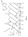
Refer to FIG. 3, the brightness enhancement film 20 of the present invention includes an optical substrate 30 adhered to a support or base layer 31. The optical substrate has a light input surface 32 that is planar and smooth, and a light output surface 34 that has a prismatic structure that may be viewed as comprising longitudinal regular prism blocks 35 arranged in lateral rows (i.e., side-by-side). In one embodiment of the present invention, the light output surface and the light input surface are generally parallel to each other in the overall optical substrate structure (i.e., do not form an overall substrate structure that is generally tapered like a light guide plate in a backlight module, or that is concave or convex). While FIG. 3 shows the base 31 to be of uniform thickness, it may be non-uniform thickness.
For ease of reference, the following orthogonal x, y, z coordinate system would be adopted in explaining the various directions. As shown in FIG. 3, the x-axis is in the direction across the peaks and valleys, also referred to as the lateral direction. The y-axis is orthogonal to the x-axis, in the plane of the substrate 30, in a generally longitudinal direction of the prism blocks 35. The prism blocks may be regular or irregular (as disclosed in copending U.S. patent application Ser. No. 11/450,145, commonly assigned to the assignee of the present invention, and is fully incorporated by reference herein). In the illustrated embodiment, the prism blocks 35 are regular in geometry. The light input surface 32 lies in an x-y plane. For a rectangular piece of the optical substrate, the x and y-axes would be along the orthogonal edges of the substrate 30. The z-axis is orthogonal to the x and y-axes. The edge showing the ends of the lateral rows of the prism blocks 35 lies in the x-z plane, such as shown in FIG. 3. References to cross sections of a prism block 35 would be sections taken in x-z planes, at various locations along the y axis. Further, references to a horizontal direction would be in an x-y plane, and references to a vertical direction would be in the z-direction. Hereinafter, references to heights of peaks and valleys are measured in the z-direction with respect to the planar surface adjoining between the substrate 30 and the base layer 31. It is noted that the references to peak vertex angles herein refer to the angles of the peak 36, and valley vertex angles herein refer to the angles of the valleys 37, as viewed along cross sections in the x-z planes at locations along the y direction, as defined above.
The prism blocks 35 each has two longitudinal facets, or longitudinal flat surfaces, forming a longitudinal peak 36. The facets 38 of adjoining prism blocks 35 intersect to define a valley 37 (which may be a high valley 37H or a low valley 37L, as will be explained later below). In the illustrated embodiment, the prism blocks 35 are shown to be substantially similar to one another, substantially symmetrical with respect to the z-axis, and have uniform cross-sections along the longitudinal direction (y-axis). The height of the valleys 37 may vary in the lateral (x) direction of the respective valleys 37, as further explained below, and may further vary in the longitudinal (y) direction. The peak vertex angles are similar (e.g., 90 to 100 degrees), and the valley vertex angles are also similar to one another (e.g., 90 to 100 degrees). It is noted that in the sectional views in x-z planes, the peak vertex angles and the valley vertex angles may be rounded instead of a sharp point, due to manufacturing constraints.
In accordance with the present invention, the bottom thickness of the material below the valleys 37 in the optical substrate 30, which defines the height of the valleys above the top surface of the base layer 31, varies across the lateral direction, from substantially zero thickness, to a defined thickness D (e.g., 0.3 to 5 micrometers). In the illustrated embodiment, the heights, or bottom thickness, of the valleys 37 vary periodically, in which the bottom thickness is D (i.e., the “high” valleys 37H) for all the valleys except for every n-th valleys (e.g., every third valleys in FIG. 3), which is substantially smaller thickness or substantially zero thickness (i.e., the “low” valleys 37L). During the forming of the structured surface of the optical substrate, if the nip roll pressure is high enough, the master mold drum may directly touch the base layer 31 at the low valleys 37L, in which case the bottom thickness would be theoretically zero for the low valleys 37L. In any event, bottom thickness of the low valleys 37L is substantially smaller than the bottom thickness of the high valleys 37H. In one embodiment, the ratio of the bottom thickness of the high valley 37H to the bottom thickness of the low valley 37L is more than about 100:1, or more than about 50:1; or more than about 40:1; or about 30:1; or more than about 30:1, or more than about 10:1.Alternatively, instead of the bottom thickness varying across the substrate in a periodic manner, the bottom thickness may vary randomly, between low valleys and high valleys, wherein the low valleys have bottom thickness that are substantially smaller than the bottom thickness of the high valleys. It is understood that the high valleys may have different bottom thicknesses among the high valleys 37H, but which are all substantially thicker than the bottom thickness of the low valleys 37L.
It is noted that for substantially symmetrical peaks 36, the distance or pitch PH between adjacent peaks 36 about a low valley is a little shorter than the pitch PL between adjacent peaks 36 about a high valley. In the illustrated embodiment in FIG. 3, the peaks 36 are mutually parallel, and the valleys 37 are mutually parallel, and further the valleys 37 and the peaks 36 are mutually parallel.
As an example to illustrate the relative dimensions of an optical substrate in accordance with the present invention, the peak heights are on the order of 10 to 200 micrometers, the valley heights (bottom thickness) are on the order of 0.3 to 5 micrometers, the width of each peak (as measured between two valleys) are on the order of 20 to 400 micrometers, the thickness of the base layer 31 is on the order of 25 to 300 micrometers. The foregoing dimensions are intended to illustrate the fact that the structured surface features are microstructures, in the micrometers range. By way of example, the overall size of the area of the optical substrate may vary on the order of 2 mm to 10 m in width and length (and even larger dimensions possible), depending on the particular application (e.g., in a flat panel display of a cellular phone, or in a significantly larger flat panel display of a TV monitor). The characteristic size of the prism blocks on the structured surface of the optical substrate need not change appreciably with different overall optical substrate size.
The optical substrate 30 may be formed with an optically transparent material, such as acrylic. The base substrate 31 may be of PET material, but may be made from the same transparent material as the optical substrate 30, which provides additional structural support to the relatively thin optical substrate 30. The optical substrate 30 may be flexible enough to be manufactured in a roll, which is laid on and bonded to the separate base substrate 31. While the thickness of the base substrate may be on the order of 25 to 300 micrometers thick, the thickness of the base substrate may be thinner or thicker than this range, depending on the particular application. Generally, though not required, larger size optical substrate may have a thicker base substrate to provide better support, and a smaller size optical substrate may require a thinner base substrate for smaller scale applications.
The anti-chatter structure of the structured optical substrate 30 may be formed by prior art processes for forming microstructures on optical substrates, which are configured to provide the varying valley bottom thicknesses in accordance with the present invention. For example, the structured surface of optical substrate of the present invention may be generated in accordance with a number of process techniques, including micromachining using hard tools to form molds or the like for the prismatic profile described above. The hard tools may be very small diamond tools mounted on CNC (Computer Numeric Control) machines (e.g. turning, milling and ruling/shaping machines). Furthermore, known STS (Slow Tool Servo) and FTS (Fast Tool Servo) are examples of the devices. U.S. Pat. No. 6,581,286, for instance, discloses one of the applications of the FTS for making grooves on an optical film by using thread cutting method. The tool is mounted onto the machine, to create constant peak vertex angle in relation to x-z planes along the y direction within a prism.
The master may be used to mold the optical substrate directly or used in electroforming a duplicate of the master, which duplicate is used to mold the optical substrate. The mold may be in the form of a belt, a drum, a plate, or a cavity. The mold may be used to form the prismatic structure on a substrate through hot embossing of the substrate, and/or through the addition of an ultraviolet curing or thermal setting materials in which the structures are formed. The substrate or coating material may be any organic, inorganic or hybrid optically transparent material and may include suspended diffusion, birefringent or index of refraction modifying particles.
It has been found that the anti-chatter structure disclosed above reduces chatter induced shades and/or lines in the displayed image, without compromising adhesion between the structured optical substrate layer 30 and the base layer 31. The structured light output surface is formed by applying a tool to form the peaks and valleys, and wherein the tool is cause to bottom out at the low valleys to press on the support layer (the tool 200 is schematically represented in FIG. 3). The bottom thickness can be relatively easy to control for the high valleys (e.g., 0.3 to 5 micrometers), by applying the nip pressure to cause the master mold drum to substantially bottom out at the low valleys to touch or press upon the harder base layer 31, thereby limiting travel of the mold drum to limit the bottom thickness of the high valleys. Further the curing process involved in the prism structure forming processes is broader for the inventive structured substrate, because the nip roll pressure does not have to be as precisely controlled (as long as the nip pressure is beyond a threshold needed to cause the master mold drum to bottom out on the base layer 31 at the low valleys), as compared to prior art structured substrates. After the layer of material (e.g., acrylic) to be used to form the structured substrate 30 is adhered to the base layer 31, and then the prism structure is formed, the process needs to provide enough pressure to create valleys with substantially zero bottom thickness (i.e., the “low” valleys), or valleys with bottom coplanar with the top surface of the base layer 31. Such low valleys essentially bottoms out at the surface of the base layer 31.
The adhesion control can be adjusted by the ratio of the number of high valleys and low valleys. For example, a design with improved adhesive may have one low valley for every adjacent six high valleys (e.g., each 2 micrometers bottom thickness). If adhesion is acceptable, there may be 4 adjacent low valleys for every six or seven adjacent high valleys.
Further, the following variations are well within the scope and spirit of the present invention. The peak and valley vertex angles may or may not vary across laterally adjoining rows. It is noted that the geometries (e.g., overall size, peak and valley angles, etc.) may be different for different prism blocks 35 in the optical substrate 30. The pitch between adjacent peaks 36, adjacent valleys 37, and/or adjacent peak 36 and valley 37 may vary in an orderly, semi-orderly, random, or quasi-random manner. It is noted that an array, pattern or configuration of a group of random irregular prism blocks may repeat over a range of area or length over the overall structured light output surface of the optical substrate 30, resulting in an overall orderly, semi-orderly or quasi-random pattern or arrangement for the overall optical substrate. Adjacent peaks, adjacent valleys, and/or adjacent peak and valley may or may not be parallel within at least a range of lateral prism blocks. The adjacent peaks 36, adjacent valleys 37, and/or adjacent peak 36 and valley 37 may alternate from parallel to non-parallel, in an orderly, semi-orderly, random, or quasi-random manner. Similarly, adjacent non-parallel peaks 36, adjacent valleys 37 and/or adjacent peak 36 and valley 37, may alternate between convergence to divergence (in reference to the same general longitudinal direction of the prism blocks), in an orderly, semi -orderly, random, or pseudo-random manner. Sections of the optical substrate 30 taken across the peaks 36 and valleys 37 in an x-z plane at various locations along the y-direction and/or in a general longitudinal direction of a particular peak or valley may or may not be constant.
In accordance with the present invention, the optical substrate comprising a prismatic, structured light output surface, which enhances brightness and reduces chatter phenomenon, when applied in an LCD for example. An LCD incorporating the inventive optical substrate in accordance with the present invention may be deployed in an electronic device. As shown in FIG. 4, an electronic 110 (which may be one of a PDA, mobile phone, television, display monitor, portable computer, refrigerator, etc.) comprises the inventive LCD 10 (FIG. 2) in accordance with one embodiment of the present invention. The LCD 10 comprises the inventive optical substrate described above. The electronic device 110 may further include within a suitable housing, a user input interface such as keys and buttons (schematically represented by the block 116), image data control electronics, such as a controller (schematically represented by block 112) for managing image data flow to the LCD panel 10, electronics specific to the electronic device 110, which may include a processor, A/D converters, memory devices, data storage devices, etc. (schematically collectively represented by block 118), and a power source such as a power supply, battery or jack for external power source (schematically represented by block 114), which components are well known in the art.
While particular embodiments of the invention have been described herein for the purpose of illustrating the invention and not for the purpose of limiting the same, it will be appreciated by those of ordinary skill in the art that numerous variations of the details, materials, and arrangements of parts may be made without departing from the scope of the invention as defined in the appended claims.

Claims (21)

1. A luminance enhancement substrate, comprising:
a support layer having a top surface; and
an optical substrate, having a planar light input surface at one side of the optical substrate, and a structured light output surface at an opposite side of the optical substrate defining a plurality of peaks and valleys defined by longitudinal prisms in the structured light output surface, wherein the light input surface is adhered to the top surface of the support layer, and wherein the distance of the plurality of valleys from the top surface varies across the optical substrate.
2. The luminance enhancement substrate as in claim 1, wherein the distance varies in a periodical manner for the valleys across the structured surface.
3. The luminance enhancement substrate as in claim 2, wherein the distance remains substantially similar for a first number of adjacent valleys, but is substantially zero over a longitudinal distance for a second number of adjacent valleys in their entirety after every first number of adjacent valleys, wherein the first number and second number of adjacent valleys are non-zero.
4. The luminance enhancement substrate as in claim 1, wherein the peaks have same height across entire substrate.
5. The luminance enhancement substrate as in claim 1, wherein the prisms are similar across the structured light output surface.
6. The luminance enhancement substrate as in claim 1, wherein the prisms are regular prisms.
7. The luminance enhancement substrate as in claim 1, wherein the prisms are each symmetrical about a longitudinal direction.
8. The luminance enhancement substrate as in claim 1, wherein some of the valleys are substantially coplanar with the top surface of the support layer, and other valleys are not coplanar with said coplanar valleys.
9. The luminance enhancement substrate as in claim 8, wherein said coplanar valleys are spaced in a periodic manner across the valleys in the structured surface.
10. A luminance enhancement substrate, comprising:
a support layer having a top surface; and
an optical substrate, having a planar light input surface at one side of the optical substrate, and a structured light output surface at an opposite side of the optical substrate defining a plurality of peaks and valleys, wherein the light input surface is adhered to the top surface of the support layer, and wherein the distance of the plurality of valleys from the top surface varies across the optical substrate,
wherein some of the valleys are substantially coplanar with the top surface of the support layer, and other valleys are not coplanar with said coplanar valleys, wherein said coplanar valleys are spaced in a periodic manner across the valleys in the structured surface, and wherein said coplanar valleys are spaced after every first number of adjacent valleys, wherein the first number of adjacent valleys is non-zero.
11. The luminance enhancement substrate as in claim 10, wherein said coplanar valleys comprise a second number of adjacent coplanar valleys after every first number of adjacent valleys, wherein the second number is non-zero.
12. The luminance enhancement substrate as in claim 1, wherein the distance for a first number of adjacent valleys is substantially larger than the distance for a second number of adjacent valleys, wherein the first number and the second number of adjacent valleys are non-zero.
13. A flat panel display, comprising:
a display module emitting light in accordance with an image; and
an optical substrate as in claim 1, enhancing brightness of the image.
14. An electronic device, comprising:
a flat panel display as in claim 13; and
control electronics directing image data to the flat panel display to render an image in accordance with the image data.
15. A method of enhancing brightness of an image rendered by a flat panel display, comprising:
providing a display module that emits light in accordance with an image; and
providing an optical substrate as in claim 1, receiving light through the light input surface and emitting light through the light output surface, whereby brightness of the image is enhanced by the structured surface.
16. A method of making a luminance enhancement substrate, comprising:
providing a support layer having a top surface;
adhering a light input surface on one side of an optical substrate layer on the top surface;
forming a structured light output surface comprising longitudinal prisms at an opposite side of the optical substrate to define a plurality of peaks and valleys, wherein the distance of the plurality of valleys from the top surface varies across the optical substrate.
17. The method as in claim 16, wherein the distance remains substantially similar for a first number of adjacent valleys, but is substantially zero over a longitudinal distance for a second number of adjacent valleys in their entirety after every first number of adjacent valleys, wherein the first number and second number of adjacent valleys are non-zero.
18. The method as in claim 16, wherein some of the valleys are substantially coplanar with the top surface of the support layer, and other valleys are not coplanar with said coplanar valleys.
19. The method as in claim 16, wherein the distance for a first number of adjacent high valleys is substantially larger than the distance for a second number of adjacent low valleys, wherein the first number and the second number of adjacent valleys are non-zero.
20. The method as in claim 19, wherein the structured light output surface is formed by applying a tool to form the peaks and valleys, and wherein the tool is cause to bottom out over a longitudinal distance at the low valleys in their entirety to press on the support layer.
21. The luminance enhancement substrate as in claim 1, wherein the optical substrate has a first edge and a second edge, wherein each longitudinal prism extends from the first edge to the second edge.
US11/635,802 2005-12-06 2006-12-06 Luminance enhancement optical substrates with anti-chatter structures Active 2027-03-25 US7712944B2 (en)

Priority Applications (1)

Application Number Priority Date Filing Date Title
US11/635,802 US7712944B2 (en) 2005-12-06 2006-12-06 Luminance enhancement optical substrates with anti-chatter structures

Applications Claiming Priority (2)

Application Number Priority Date Filing Date Title
US74295905P 2005-12-06 2005-12-06
US11/635,802 US7712944B2 (en) 2005-12-06 2006-12-06 Luminance enhancement optical substrates with anti-chatter structures

Publications (2)

Publication Number Publication Date
US20080049451A1 US20080049451A1 (en) 2008-02-28
US7712944B2 true US7712944B2 (en) 2010-05-11

Family

ID=37887879

Family Applications (1)

Application Number Title Priority Date Filing Date
US11/635,802 Active 2027-03-25 US7712944B2 (en) 2005-12-06 2006-12-06 Luminance enhancement optical substrates with anti-chatter structures

Country Status (3)

Country Link
US (1) US7712944B2 (en)
TW (1) TWI339743B (en)
WO (1) WO2007067692A1 (en)

Cited By (2)

* Cited by examiner, † Cited by third party
Publication number Priority date Publication date Assignee Title
US20150117052A1 (en) * 2013-10-29 2015-04-30 Au Optronics Corporation Backlight Module and Display Panel using the same
CN105572790A (en) * 2010-03-26 2016-05-11 友辉光电股份有限公司 Optical substrate, uneven structure and method for forming uneven structure on substrate

Families Citing this family (9)

* Cited by examiner, † Cited by third party
Publication number Priority date Publication date Assignee Title
CN101743488B (en) * 2007-07-17 2014-02-26 科锐公司 Optical elements with internal optical features and methods of fabricating same
US20090091937A1 (en) * 2007-10-05 2009-04-09 Tien-Hon Chiang Light control device having irregular prism surface
KR101859413B1 (en) * 2011-12-26 2018-05-21 삼성디스플레이 주식회사 A display module and an apparatus having the same
TW201345339A (en) * 2012-04-17 2013-11-01 Tera Xtal Technology Corp Touch panel
CN103376933A (en) * 2012-04-20 2013-10-30 鑫晶钻科技股份有限公司 Touch panel
CN108474877A (en) * 2015-12-28 2018-08-31 3M创新有限公司 Product with microstructured layer
JP2019501802A (en) 2015-12-28 2019-01-24 スリーエム イノベイティブ プロパティズ カンパニー Article having a microstructured layer
KR20180089538A (en) 2015-12-28 2018-08-08 쓰리엠 이노베이티브 프로퍼티즈 컴파니 An article having a microstructured layer
US20180354225A1 (en) * 2015-12-28 2018-12-13 3M Innovative Properties Company Article with microstructed layer

Citations (38)

* Cited by examiner, † Cited by third party
Publication number Priority date Publication date Assignee Title
US4542449A (en) 1983-08-29 1985-09-17 Canadian Patents & Development Limited Lighting panel with opposed 45° corrugations
US5005108A (en) 1989-02-10 1991-04-02 Lumitex, Inc. Thin panel illuminator
US5175030A (en) 1989-02-10 1992-12-29 Minnesota Mining And Manufacturing Company Microstructure-bearing composite plastic articles and method of making
US5183597A (en) 1989-02-10 1993-02-02 Minnesota Mining And Manufacturing Company Method of molding microstructure bearing composite plastic articles
US5280371A (en) 1992-07-09 1994-01-18 Honeywell Inc. Directional diffuser for a liquid crystal display
US5579163A (en) 1994-12-23 1996-11-26 Peterson; Jeffrey M. Method and apparatus for producing spectral displays
US5771328A (en) * 1995-03-03 1998-06-23 Minnesota Mining And Manufacturing Company Light directing film having variable height structured surface and light directing article constructed therefrom
US5779337A (en) 1996-05-13 1998-07-14 Konica Corporation Plane light source unit and light guide used therein
US5851062A (en) 1995-08-11 1998-12-22 Omron Corporation Prism sheet for surface light source
US5917664A (en) 1996-02-05 1999-06-29 3M Innovative Properties Company Brightness enhancement film with soft cutoff
US5919551A (en) 1996-04-12 1999-07-06 3M Innovative Properties Company Variable pitch structured optical film
WO1999036248A2 (en) 1998-01-13 1999-07-22 Minnesota Mining And Manufacturing Company Process for making multilayer optical films
WO1999042861A1 (en) 1998-02-18 1999-08-26 Minnesota Mining And Manufacturing Company Optical film
US6091547A (en) 1994-09-27 2000-07-18 3M Innovative Properties Company Luminance control film
US20010011779A1 (en) 1998-01-13 2001-08-09 3M Innovative Properties Company Method for making textured multilayer optical films
US6330386B1 (en) 1996-12-16 2001-12-11 Robert Bosch Gmbh Lightening unit
US20010053075A1 (en) 1999-02-23 2001-12-20 Parker Jeffery R. Light redirecting films and film systems
US20020057497A1 (en) 1999-10-08 2002-05-16 3M Innovative Properties Company Optical film with variable angle prisms
US20020146296A1 (en) 2001-02-26 2002-10-10 National Institute Of Standards And Technology Method and device for avoiding chatter during machine tool operation
US20030103760A1 (en) 1999-10-08 2003-06-05 Mark E. Gardiner Optical element having programmed optical structures
US20030227768A1 (en) 2002-06-11 2003-12-11 Fujitsu Limited Electronic apparatus, liquid crystal display device and light guide plate
US20040061944A1 (en) 1997-04-22 2004-04-01 Dai Nippon Printing Co., Ltd. Optical sheet lamination
US20040090572A1 (en) 2002-11-11 2004-05-13 Byung-Woong Han Prism sheet and fabrication method thereof and liquid crystal display device employing the same
US20040105157A1 (en) 2002-09-30 2004-06-03 Motohiko Matsushita Optical component for liquid crystal display
EP1455203A1 (en) 2001-11-07 2004-09-08 International Business Machines Corporation Prism sheet, back light unit using the prism sheet, and transmissive liquid crystal display device
US6797366B2 (en) 1998-01-13 2004-09-28 3M Innovative Properties Company Color shifting film articles
US20040190102A1 (en) 2000-08-18 2004-09-30 Mullen Patrick W. Differentially-cured materials and process for forming same
US20040246599A1 (en) 2003-05-02 2004-12-09 Reflexite Corporation Light-redirecting optical structures
US20050024849A1 (en) 1999-02-23 2005-02-03 Parker Jeffery R. Methods of cutting or forming cavities in a substrate for use in making optical films, components or wave guides
US6862141B2 (en) 2002-05-20 2005-03-01 General Electric Company Optical substrate and method of making
WO2005026793A1 (en) 2003-09-12 2005-03-24 3M Innovative Properties Company Durable optical element
US20050122591A1 (en) 1999-02-23 2005-06-09 Parker Jeffery R. Light redirecting films and film systems
US20050140860A1 (en) 2003-12-31 2005-06-30 General Electric Company Display optical films
US20050141243A1 (en) 2000-08-18 2005-06-30 Reflexite Corporation Differentially-cured materials and process for forming same
US20050280752A1 (en) 2004-06-22 2005-12-22 Dong-Hoon Kim Optical film, backlight assembly and liquid crystal display device having the same
US20060047358A1 (en) 2004-08-31 2006-03-02 General Electric Company Machine tool control methods and designs for fabricating mesoscopic surface structures on substrates
WO2006073033A1 (en) 2005-01-06 2006-07-13 Sharp Kabushiki Kaisha Lamp clip, lighting system for display device, and display device
US7269327B2 (en) * 2005-06-30 2007-09-11 Efun Technology Co., Ltd Brightness enhancement film having a reinforcing structure

Patent Citations (48)

* Cited by examiner, † Cited by third party
Publication number Priority date Publication date Assignee Title
US4542449A (en) 1983-08-29 1985-09-17 Canadian Patents & Development Limited Lighting panel with opposed 45° corrugations
US5005108A (en) 1989-02-10 1991-04-02 Lumitex, Inc. Thin panel illuminator
US5175030A (en) 1989-02-10 1992-12-29 Minnesota Mining And Manufacturing Company Microstructure-bearing composite plastic articles and method of making
US5183597A (en) 1989-02-10 1993-02-02 Minnesota Mining And Manufacturing Company Method of molding microstructure bearing composite plastic articles
US5280371A (en) 1992-07-09 1994-01-18 Honeywell Inc. Directional diffuser for a liquid crystal display
US6091547A (en) 1994-09-27 2000-07-18 3M Innovative Properties Company Luminance control film
US5579163A (en) 1994-12-23 1996-11-26 Peterson; Jeffrey M. Method and apparatus for producing spectral displays
US5771328A (en) * 1995-03-03 1998-06-23 Minnesota Mining And Manufacturing Company Light directing film having variable height structured surface and light directing article constructed therefrom
US5851062A (en) 1995-08-11 1998-12-22 Omron Corporation Prism sheet for surface light source
US5917664A (en) 1996-02-05 1999-06-29 3M Innovative Properties Company Brightness enhancement film with soft cutoff
US5919551A (en) 1996-04-12 1999-07-06 3M Innovative Properties Company Variable pitch structured optical film
US5779337A (en) 1996-05-13 1998-07-14 Konica Corporation Plane light source unit and light guide used therein
US6330386B1 (en) 1996-12-16 2001-12-11 Robert Bosch Gmbh Lightening unit
US20040061944A1 (en) 1997-04-22 2004-04-01 Dai Nippon Printing Co., Ltd. Optical sheet lamination
US20010011779A1 (en) 1998-01-13 2001-08-09 3M Innovative Properties Company Method for making textured multilayer optical films
US6827886B2 (en) 1998-01-13 2004-12-07 3M Innovative Properties Company Method for making multilayer optical films
US20010022982A1 (en) 1998-01-13 2001-09-20 3M Innovative Properties Company Apparatus for making multilayer optical films
US6783349B2 (en) 1998-01-13 2004-08-31 3M Innovative Properties Company Apparatus for making multilayer optical films
US6797366B2 (en) 1998-01-13 2004-09-28 3M Innovative Properties Company Color shifting film articles
WO1999036248A2 (en) 1998-01-13 1999-07-22 Minnesota Mining And Manufacturing Company Process for making multilayer optical films
US6808658B2 (en) 1998-01-13 2004-10-26 3M Innovative Properties Company Method for making texture multilayer optical films
US20050110175A1 (en) 1998-01-13 2005-05-26 3M Innovative Properties Company Method for making textured multilayer optical films
US20010013668A1 (en) 1998-01-13 2001-08-16 3M Innovative Properties Company Method for making multilayer optical films
WO1999042861A1 (en) 1998-02-18 1999-08-26 Minnesota Mining And Manufacturing Company Optical film
US6354709B1 (en) 1998-02-18 2002-03-12 3M Innovative Properties Company Optical film
US20050024849A1 (en) 1999-02-23 2005-02-03 Parker Jeffery R. Methods of cutting or forming cavities in a substrate for use in making optical films, components or wave guides
US20050122591A1 (en) 1999-02-23 2005-06-09 Parker Jeffery R. Light redirecting films and film systems
US20010053075A1 (en) 1999-02-23 2001-12-20 Parker Jeffery R. Light redirecting films and film systems
US20050001043A1 (en) 1999-10-08 2005-01-06 3M Innovative Properties Company Optical elements having programmed optical structures
US20030103760A1 (en) 1999-10-08 2003-06-05 Mark E. Gardiner Optical element having programmed optical structures
US20020057497A1 (en) 1999-10-08 2002-05-16 3M Innovative Properties Company Optical film with variable angle prisms
US20030112521A1 (en) 1999-10-08 2003-06-19 3M Optical film with variable angle prisms
US6707611B2 (en) 1999-10-08 2004-03-16 3M Innovative Properties Company Optical film with variable angle prisms
US20050141243A1 (en) 2000-08-18 2005-06-30 Reflexite Corporation Differentially-cured materials and process for forming same
US20040190102A1 (en) 2000-08-18 2004-09-30 Mullen Patrick W. Differentially-cured materials and process for forming same
US20020146296A1 (en) 2001-02-26 2002-10-10 National Institute Of Standards And Technology Method and device for avoiding chatter during machine tool operation
EP1455203A1 (en) 2001-11-07 2004-09-08 International Business Machines Corporation Prism sheet, back light unit using the prism sheet, and transmissive liquid crystal display device
US6862141B2 (en) 2002-05-20 2005-03-01 General Electric Company Optical substrate and method of making
US20030227768A1 (en) 2002-06-11 2003-12-11 Fujitsu Limited Electronic apparatus, liquid crystal display device and light guide plate
US20040105157A1 (en) 2002-09-30 2004-06-03 Motohiko Matsushita Optical component for liquid crystal display
US20040090572A1 (en) 2002-11-11 2004-05-13 Byung-Woong Han Prism sheet and fabrication method thereof and liquid crystal display device employing the same
US20040246599A1 (en) 2003-05-02 2004-12-09 Reflexite Corporation Light-redirecting optical structures
WO2005026793A1 (en) 2003-09-12 2005-03-24 3M Innovative Properties Company Durable optical element
US20050140860A1 (en) 2003-12-31 2005-06-30 General Electric Company Display optical films
US20050280752A1 (en) 2004-06-22 2005-12-22 Dong-Hoon Kim Optical film, backlight assembly and liquid crystal display device having the same
US20060047358A1 (en) 2004-08-31 2006-03-02 General Electric Company Machine tool control methods and designs for fabricating mesoscopic surface structures on substrates
WO2006073033A1 (en) 2005-01-06 2006-07-13 Sharp Kabushiki Kaisha Lamp clip, lighting system for display device, and display device
US7269327B2 (en) * 2005-06-30 2007-09-11 Efun Technology Co., Ltd Brightness enhancement film having a reinforcing structure

Non-Patent Citations (3)

* Cited by examiner, † Cited by third party
Title
International Search Report of Counterpart PCT Application No. PCT/US2006/046689.
International Search Report of Related Case PCT Application No. PCT/US2006/022812.
International Search Report of Related Case PCT Application No. PCT/US2007/015364.

Cited By (4)

* Cited by examiner, † Cited by third party
Publication number Priority date Publication date Assignee Title
CN105572790A (en) * 2010-03-26 2016-05-11 友辉光电股份有限公司 Optical substrate, uneven structure and method for forming uneven structure on substrate
CN105572790B (en) * 2010-03-26 2021-07-13 友辉光电股份有限公司 Optical sheet, concave-convex structure and method for forming concave-convex structure on substrate
US20150117052A1 (en) * 2013-10-29 2015-04-30 Au Optronics Corporation Backlight Module and Display Panel using the same
US9323105B2 (en) * 2013-10-29 2016-04-26 Au Optronics Corporation Backlight module and display panel using the same

Also Published As

Publication number Publication date
WO2007067692A1 (en) 2007-06-14
US20080049451A1 (en) 2008-02-28
TWI339743B (en) 2011-04-01
TW200722792A (en) 2007-06-16

Similar Documents

Publication Publication Date Title
US7712944B2 (en) Luminance enhancement optical substrates with anti-chatter structures
US9804403B2 (en) Moire reducing optical substrates with irregular prism structures
US7883647B2 (en) Method of making luminance enhancement optical substrates with optical defect masking structures
US10527775B2 (en) Optical substrates having light collimating and diffusion structures
US9180609B2 (en) Optical substrates having light collimating and diffusion structures
CN102213788B (en) There is the optical substrate of optical alignment and diffusing structure
US8899768B2 (en) Luminance enhancement film having a substrate incorporating dispersed particles for diffusion
KR20110134297A (en) Light guide film
US10725330B2 (en) Optical substrates having light collimating and diffusion structures
US9075178B2 (en) Luminance enhancement optical substrates with anti-interference-fringe structures
US9733400B2 (en) Light directing film
US10379268B2 (en) Light directing film
US9841541B2 (en) Luminance enhancement film having a substrate incorporation dispersed particles for diffusion
TW201514550A (en) Luminance enhancement optical substrates with anit-interference-fringe structure

Legal Events

Date Code Title Description
AS Assignment

Owner name: UBRIGHT OPTRONICS CORPORATION, TAIWAN

Free format text: ASSIGNMENT OF ASSIGNORS INTEREST;ASSIGNORS:WANG, KONG-HUA;LIN, CRAIG;KO, DANIEL YAW-CHUNG;REEL/FRAME:019061/0451;SIGNING DATES FROM 20070305 TO 20070307

Owner name: UBRIGHT OPTRONICS CORPORATION,TAIWAN

Free format text: ASSIGNMENT OF ASSIGNORS INTEREST;ASSIGNORS:WANG, KONG-HUA;LIN, CRAIG;KO, DANIEL YAW-CHUNG;SIGNING DATES FROM 20070305 TO 20070307;REEL/FRAME:019061/0451

STCF Information on status: patent grant

Free format text: PATENTED CASE

FPAY Fee payment

Year of fee payment: 4

MAFP Maintenance fee payment

Free format text: PAYMENT OF MAINTENANCE FEE, 8TH YEAR, LARGE ENTITY (ORIGINAL EVENT CODE: M1552)

Year of fee payment: 8

FEPP Fee payment procedure

Free format text: ENTITY STATUS SET TO SMALL (ORIGINAL EVENT CODE: SMAL); ENTITY STATUS OF PATENT OWNER: SMALL ENTITY

MAFP Maintenance fee payment

Free format text: PAYMENT OF MAINTENANCE FEE, 12TH YR, SMALL ENTITY (ORIGINAL EVENT CODE: M2553); ENTITY STATUS OF PATENT OWNER: SMALL ENTITY

Year of fee payment: 12