US7714943B2 - Ultra-thin image projection system - Google Patents
Ultra-thin image projection system Download PDFInfo
- Publication number
- US7714943B2 US7714943B2 US11/585,107 US58510706A US7714943B2 US 7714943 B2 US7714943 B2 US 7714943B2 US 58510706 A US58510706 A US 58510706A US 7714943 B2 US7714943 B2 US 7714943B2
- Authority
- US
- United States
- Prior art keywords
- mirror
- image
- screen
- lens
- housing
- Prior art date
- Legal status (The legal status is an assumption and is not a legal conclusion. Google has not performed a legal analysis and makes no representation as to the accuracy of the status listed.)
- Active, expires
Links
Images


Classifications
-
- H—ELECTRICITY
- H04—ELECTRIC COMMUNICATION TECHNIQUE
- H04N—PICTORIAL COMMUNICATION, e.g. TELEVISION
- H04N9/00—Details of colour television systems
- H04N9/12—Picture reproducers
- H04N9/31—Projection devices for colour picture display, e.g. using electronic spatial light modulators [ESLM]
- H04N9/3141—Constructional details thereof
-
- G—PHYSICS
- G03—PHOTOGRAPHY; CINEMATOGRAPHY; ANALOGOUS TECHNIQUES USING WAVES OTHER THAN OPTICAL WAVES; ELECTROGRAPHY; HOLOGRAPHY
- G03B—APPARATUS OR ARRANGEMENTS FOR TAKING PHOTOGRAPHS OR FOR PROJECTING OR VIEWING THEM; APPARATUS OR ARRANGEMENTS EMPLOYING ANALOGOUS TECHNIQUES USING WAVES OTHER THAN OPTICAL WAVES; ACCESSORIES THEREFOR
- G03B21/00—Projectors or projection-type viewers; Accessories therefor
- G03B21/14—Details
- G03B21/28—Reflectors in projection beam
-
- G—PHYSICS
- G03—PHOTOGRAPHY; CINEMATOGRAPHY; ANALOGOUS TECHNIQUES USING WAVES OTHER THAN OPTICAL WAVES; ELECTROGRAPHY; HOLOGRAPHY
- G03B—APPARATUS OR ARRANGEMENTS FOR TAKING PHOTOGRAPHS OR FOR PROJECTING OR VIEWING THEM; APPARATUS OR ARRANGEMENTS EMPLOYING ANALOGOUS TECHNIQUES USING WAVES OTHER THAN OPTICAL WAVES; ACCESSORIES THEREFOR
- G03B21/00—Projectors or projection-type viewers; Accessories therefor
- G03B21/54—Accessories
- G03B21/56—Projection screens
- G03B21/60—Projection screens characterised by the nature of the surface
- G03B21/62—Translucent screens
-
- H—ELECTRICITY
- H04—ELECTRIC COMMUNICATION TECHNIQUE
- H04N—PICTORIAL COMMUNICATION, e.g. TELEVISION
- H04N9/00—Details of colour television systems
- H04N9/12—Picture reproducers
- H04N9/31—Projection devices for colour picture display, e.g. using electronic spatial light modulators [ESLM]
- H04N9/3129—Projection devices for colour picture display, e.g. using electronic spatial light modulators [ESLM] scanning a light beam on the display screen
Definitions
- a rear projection display system comprising:
- a screen having a screen diagonal and a screen normal direction, positioned at a front side of the housing;
- a light engine placed inside the housing, having an illumination stage adapted to create a beam of light, at least one display panel adapted to modulate the beam of light to create an image, and a lens system having a focal length and adapted to project the created image forming a projected image consisting of light rays;
- a non-rotationally symmetric first mirror placed inside the housing and in the optical path of said projected image, having dimensions significantly smaller than said screen diagonal, and having a horizontally convex curvature, and having a vertical curvature which is a function of the focal length of said lens system, such that for shorter focal length it is more concave and less convex, and for longer focal length, it is less concave and more convex, said first mirror adapted to reflect the projected image which is projected from said lens system;
- a non-rotationally symmetric second mirror placed inside the housing and in the optical path of said projected image, having dimensions significantly larger than said first mirror and smaller than said screen diagonal and having a vertical curvature which is a function of the size of the image in the absence of said second mirror relative to the size of the screen, such that for smaller image size it is convex and for larger image size it is concave, said second mirror adapted to reflect the projected image, which is reflected off of the first mirror, onto the screen to form a viewable image.
- FIG. 1 is a schematic diagram of a prior art short-throw on-axis RPDS
- FIG. 2 is a schematic diagram of a prior art off-axis projection with lens offset and flat bending mirror
- FIG. 3 is a schematic diagram of a prior art off-axis projection with lens offset and 2 curved mirrors
- FIG. 4 is graphical representation of the distortion plot with flattening of one or both mirrors in prior art RPDS
- FIG. 5 is graphical representation of a distortion plot with both mirrors properly curved in prior art RPDS
- FIG. 6 is the side view of side-firing light engine ultra-thin configuration per present invention.
- FIG. 7 is the side view of side-firing light engine ultra-thin configuration with rays in accordance with the present invention.
- FIG. 8 is the top view of side-firing light engine ultra-thin configuration in accordance with the present invention.
- FIG. 9 is the side view of top-firing light engine ultra-thin configuration in accordance with the present invention.
- FIG. 10 is the side view of top-firing light engine ultra-thin configuration with rays in accordance with the present invention.
- FIG. 11 is graphical representation of the distortion plot after flattening one mirror in an ultra-thin configuration in accordance with the present invention.
- FIG. 12 is graphical representation of the distortion plot with both mirrors properly curved in an ultra-thin configuration in accordance with the present invention.
- FIG. 13 is graphical representation of the surface profile of a first curved mirror in accordance with the present invention.
- FIG. 14 is graphical representation of the surface profile of second curved mirror in accordance with the present invention.
- FIG. 15 is side view of an exemplary super wide-angle lens used in prior art thin-chassis RPTV;
- FIG. 16 is schematic diagram of an example of a hybrid Fresnel lens used in prior art
- FIG. 17 is schematic diagram of an example of a circular TIR Fresnel lens used in one example of the present invention.
- FIG. 18 is schematic diagram of an example of stray ray generation in a circular TIR Fresnel lens
- FIG. 19 is graphical representation of the range of incidence angles on a screen in one example of the present invention.
- FIG. 20 is a block diagram of an exemplary RPDS.
- FIG. 21 is a block diagram of an example implementation of the image processor of FIG. 20 .
- RPDS rear projection display system
- a flat bending mirror 42 folds the on-axis light path, giving rise to a conventional thickness housing. It is well known that, for an RPDS to comply with desirable commercial standards, it must have a thin and compact housing. This “compactness” is quantified in terms of the “diagonal to depth ratio” or D-to-d ratio.
- the D-to-d ratio of a projection system is given by the screen diagonal length D (not shown) of a screen 20 divided by the thickness of the housing or projection distance d (shown in FIG. 1 ). The diagonal D is measured from the opposite corners of the screen 20 .
- the D-to-d ratio is given by equation 1.
- off-axis projection In RPDS designs, often off-axis projection is used to increase the D-to-d ratio. Off-axis projection, as is well known, causes a type of distortion known as keystone or trapezoidal distortion due to the resemblance of projected rectangles to keystones or trapezoids. In the RPDS design shown in FIG. 2 , off-axis projection gives an optical path, which is folded with a flat mirror and an offset between the lens and micro-display is used to correct the resulting keystone distortion. It is possible, as shown in FIG. 3 , to use two curved mirrors 42 and 43 , to fold the optical path further. Using lens offset to correct for keystone distortion rapidly leads to diminishing returns as the lens diameter and field angle increase, making the lens more expensive.
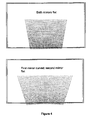
- FIG. 4 is an illustration of projected images for an off-axis RPDS similar to that shown in FIG. 3 ; the left hand image shows the effect of flattening both mirrors in such a system, resulting in keystone distortion.
- the right hand image shows the effect of the curvature of only the small mirror; clearly the convexity of the mirror allows the image to cover more of the screen.
- there is residual keystone distortion and portions of the image (the white areas within the screen borders which are not covered by grid dots) are unused (resulting in loss of brightness and loss of the use of peripheral pixels).
- the large curved mirror is also used to correct some more of the distortion.
- the curvature is selected such that the bottom of the image is expanded laterally to a greater extent than portions of the image further up.
- RPDS 100 comprises light engine 160 , first mirror 130 , flat mirror 150 , second mirror 140 , and a screen 120 .
- the light engine 160 includes one or more micro-display devices 162 and a lens assembly 164 .
- the structure is held in a housing that is not shown.
- a combination of uniquely sized, shaped and positioned mirrors is used to optimize the D-to-d ratio to approximately 11:1. With such a D-to-d ratio, an RPDS built according to the present invention, has the appearance of a large direct view LCD or plasma display system while being more economical and lighter.
- light engine 160 is generally located at the bottom portion of the housing of the RPDS 100 . However, as shown in a top view in FIG. 8 , light engine 160 is positioned with its length parallel to the screen length. This is necessary in order to keep the light engine within the housing while keeping the housing thickness low. In this embodiment, flat mirror 150 is used to turn the projected image by 90 degrees. The light engine and projection lens are therefore positioned sideways to keep them within the confines of the thin housing.
- a rectangular shaped beam of light is generated by an illumination subsystem 168 (not shown).
- the beam of light is then modulated by the micro-display device (or devices) 162 .
- the beam of light from the illumination subsystem 168 can be modulated during transmission through, or reflection from the micro-display device 162 .
- micro-display device technologies include transmissive designs, such as High Temperature PolySilicon (HTPS) LCD micro-display devices (developed by Seiko-Epson and Sony Corp), or reflective designs, such as MEMS (Micro-Electronic Mechanical Systems) and LCoS (Liquid Crystal on Silicon) micro-display devices.
- HTPS High Temperature PolySilicon
- MEMS Micro-Electronic Mechanical Systems
- LCoS Liquid Crystal on Silicon
- MEMS device An example of a MEMS device is the DMD (Digital Micro-mirror Display) device developed by Texas Instruments. Examples of LCoS devices are the SXRD devices from Sony Corp. or D-ILA devices from JVC Corp. Single panel or multi-panel micro-display device based light engines can also be used, so in some implementations, light engine 160 can include more than one micro-display device, each of which modulates a different primary color.
- Micro-display device 162 receives digital input image data from an input interface and uses the data to modulate a rectangular-shaped beam of light in order to produce a final image which is eventually displayed on the screen 120 .
- light engine 160 is generally positioned at the bottom portion of the housing.
- the light engine is positioned parallel to the length of the screen, as shown in FIG. 8 , without intruding above the lower edge of screen 120 .
- the light engine 160 is aligned along the horizontal dimension of the RPDS to keep it within the confines of the housing.
- a flat mirror 150 is then used to reflect the beam onto first mirror 130 .
- light engine 160 is generally positioned at the top portion of the housing.
- light engine 160 is positioned without protruding above screen 120 .
- the position of light engine 160 at the top of the housing facilitates convective heat dissipation without affecting other components.
- This heat if not properly managed or dissipated, can cause temperature rises which may deform various optical elements in the system and cause image distortion, focus problems and other visible artifacts in the image.
- Flat mirror 150 in this example, is used to reflect the beam, redirecting the image onto first mirror 130 as shown in the figure.
- lens assembly 164 which is positioned right after micro-display device 162 .
- lens assembly 164 does not need to be complex. A smaller number of lens elements may be used.
- the magnification of the image is achieved via the long light path and the reduced field angle of this configuration inherently reduces aberrations including distortion and lateral color shifts.
- first mirror 130 and second mirror 140 along with the prescription of the lens assembly are crucial in the design of the present invention.
- Different lens designs and mirror profiles can yield different system goals.
- the lens could be comprised of mostly or all-spherical lens elements, for lowered cost and shorter lens assembly times. This would however entail more complex curved mirror profiles.
- Mirror profile curvatures can be distributed between the two mirrors in different ways for different needs.
- the ultra-thin RPDS design of the present invention benefits greatly from having a light engine that is compact in order to fit within the confines of the housing without any special optical, mechanical, or other measures taken to ensure that they do fit.
- the illumination subsystem 168 There are two subassemblies in light engine 160 that can cause difficulties in making it fit easily: the illumination subsystem 168 , and the projection lens assembly 164 .
- Traditional illumination subsystems consist of either high intensity discharge (HID) ultra high pressure (UHP) mercury lamps (which typically have low spectral emissivity in the red wavelengths, and peaky emissivity everywhere else) or broad emission spectrum lamps such as xenon and microwave plasma lamps. In all these cases, the light is created by a plasma fireball.
- a projection lens assembly consists of multiple elements and its dimensions are dictated by the size of the light modulator (typically 0.5′′ to 1.5′′ in diagonal), the amount of offset (100% offset doubles the lens entrance pupil diameter), the amount of magnification required (the larger the screen and/or the smaller the micro-display, the longer and more expensive the lens assembly becomes), and whether the lens assembly is folded or not.
- a folded lens assembly includes an additional front surface mirror (FSM) allowing the lens to fit in a smaller space.
- FSM front surface mirror
- the light path may be folded or rotated depending on how the lens assembly needs to be fitted within the cabinet. Folding may involve a vertical inversion of the image. Rotation involves exchanging the rows/columns of the image data.
- RPDS 100 achieves a D-to-d ratio of about 11:1.
- housing depths are from 4 to 8 inches. This imposes a severe constraint on the mechanical dimensions of illumination subsystem 168 and lens assembly 164 . Since the lens assembly itself is likely to need multiple lens elements, most of the housing depth space available is already occupied. Accordingly, in the example shown in FIG. 8 , light engine 160 needs to be positioned sideways within and along the length of the housing. The light engine then projects through a turning flat mirror 150 whose sole purpose is to reposition the light engine sideways within the cabinet. In this exemplary embodiment, light engine 160 can be longer, however, obviously it still cannot be wider than 4 to 8 inches.
- the illumination subsystem 168 is provided by three (or more) solid state red, green, and blue LEDs.
- the illumination subsystem 168 is provided by three (or more) solid state red, green, and blue lasers.
- any kind of lasers or LEDs providing a combination of any set of primary colors could be used without departing from the scope of the present invention.
- LED and laser light sources can be switched very rapidly and can therefore eliminate the need for a color wheel in field-sequential light modulation schemes. Both types of light source have low power requirements and can improve color gamut. LEDs may have to be screened for desirable wavelengths (that lie close to the CIE spectrum locus curve).
- Lasers are inherently monochromatic, and thus lie on the CIE spectrum locus. With properly chosen wavelengths, they can provide a greatly increased color gamut and their wavelength, being determined by material properties, does not drift. Lasers generate polarized light, an advantage in multi-panel LCD or LCoS systems as these require polarized light anyway, so there is a further opportunity for component reduction. Lasers are suitable for RPDSs (as opposed to front projection devices) because the enclosure protects the user against potential eye and/or skin damage. Lasers have an etendue advantage over all other light sources because the emitting region can be considered almost a true point source. This allows lenses with relatively high f# to efficiently collect the light from a laser emitter, resulting in some optics cost savings. LED emitters are not quite that small and, like UHP lamp fireball dimensions, limit the etendue of the system.
- DLP micro-displays modulate light by mechanically reflecting the light from every pixel through a lens or into a dump zone (for wasted light) according to whether the pixel is on or off.
- the shade is determined by changing the proportion of time duration that the pixel is on or off.
- LCD and LCoS based RPDSs need polarized light because the light modulation works by rotating the polarized light through a further 90 degrees or not. Analyzers allow this light to continue into the lens or stop it, or the light either passes through or is reflected from a surface with dichroic coatings.
- the image is projected by the lens assembly 164 , which is positioned right after the micro-display device 162 , onto the flat mirror 150 and then onto first mirror 130 .
- First mirror 130 is used in combination with second mirror 140 and lens assembly 164 to correct for the geometric distortions of the final image that is to be displayed on the screen 120 .
- FIGS. 4 and 11 To understand the effect of the importance of the proper shape, profile, and size of the two mirrors reference is made to FIGS. 4 and 11 . If both first mirror 130 and second mirror 140 were flat, the resulting image would look very similar to that shown in FIG. 4 . Meanwhile, FIG.
- FIG. 11 is an illustration of a projected image that is produced if only second mirror 140 was flat and only first mirror 130 was properly shaped.
- FIG. 12 is an illustration of a projected image that is produced by the off-axis RPDS 100 of the present invention on the screen 120 if both mirrors 130 and 140 are curved with specific sizes and profiles chosen to be similar to those shown in FIGS. 13 and 14 respectively.
- FIG. 13 is an illustration of the profile of first mirror 130 built according to one example of the invention.
- First mirror 130 is significantly smaller than the screen 120 .
- First mirror 130 has dimensions significantly smaller than screen 120 . It has a horizontally convex curvature in order to expand the image along the length of screen 120 .
- the horizontal curvature of first mirror 130 is such that in its lower portion, which reflects the lower part of the image, it is more convex and less concave than the upper portion. This is for partial correction of the off-axis keystone effect.
- first mirror 130 has a vertical curvature which is a function of the focal length of the lens assembly 164 . For shorter focal length systems, first mirror 130 is more concave and less convex, and for longer focal length designs, it is less concave and more convex.
- FIG. 14 is an illustration of the profile of second mirror 140 which is significantly larger than first mirror 130 but smaller than the size of screen 120 .
- Keystone distortion similar to that shown in FIG. 4 is largely corrected, and the image is sized to fit the screen 120 exactly with minimal visual distortion. This residual distortion is corrected with electronics as explained below.
- the importance of matching the projected image to the size of the screen is to avoid losing pixel resolution (by turning off unused pixels) and brightness (turning off the unused pixels results in less light throughput).
- FIG. 14 is an illustration of an example for the surface curvature or profile of the second mirror 140 . It is a non-rotationally symmetric mirror having dimensions significantly larger than first mirror 130 and smaller than screen 120 .
- the function of second mirror 140 is, in addition to adjusting the vertical size of the image, to expand the vertical spacing of pixels on the bottom portion of the image relative to the top portion of the image. Accordingly, the vertical profile is shaped such that second mirror 140 has a vertical curvature that changes from less convex (or more concave) on the top portion, gradually changing to more convex (or less concave) toward the bottom portion.
- the amount of the curvature depends on the size of the image on the screen in the absence of second mirror 140 which, in turn, depends on the lens assembly focal length and the shape of first mirror 130 . If the image needs vertical magnification to fill the screen at the top, then second mirror 140 needs to be vertically convex throughout. However, if in the absence of second mirror 140 , the image vertically fills the screen or is larger, then second mirror 140 is concave at the top portion and convex at the lower portion
- second mirror 140 has a horizontally convex curvature on its upper surface that smoothly increases its degree of convex curvature towards its lower surface; in other words, it has a large horizontal radius of (convex) curvature on its upper portion and progressively smaller horizontal radii of curvature towards its lower portion.
- This profile has been designed to correct for the distortions created by projection geometry, most of which result from the off-axis nature of the RPDS 100 .
- second mirror 140 is designed to have a slightly horizontally convex upper portion to slightly expand the image to fit across the entire width of the upper portion of the screen 120 .
- Second mirror 140 is also designed to have a much more convex lower portion to expand the image to horizontally fit the width at the lower portion of the screen 120 .
- the transition between the top of second mirror 140 and the bottom of this mirror is smooth and gradual, corresponding to the keystone shape of the uncorrected image.
- second mirror 140 is designed to have a slight vertical concave curvature to slightly shrink the image in the vertical direction to equalize the line spacing in the image between the top and bottom. Unlike the horizontal expansion of the image which is dramatically different for the upper and lower portions of the image, the vertical shrinking of the image is symmetric.
- the second mirror 140 therefore, in this exemplary implementation, has an axis of symmetry extending from an upper middle portion to a lower middle portion. It is clear that in this exemplary implementation, second mirror 140 is not spherically or even rotationally symmetric.
- the vertical position of the light engine 160 is adjusted such that the keystone effect from the off-axis projection gives rise to an upper portion of the final image with exactly the same width as the upper portion of the screen 120 .
- the upper portion of the second mirror 140 is nearly flat which reduces the complexity of the design and manufacture of the second mirror 140 .
- Some prior art ultra-thin RPDS designs use a very wide-angle lens and a lens offset to make the housing thinner.
- An example of the full field in such an example is shown in FIG. 15 (no offset shown).
- the micro-display panel is smaller than the field shown and offset to one side in actual use.
- These lens assemblies could have 20-30 optical elements and are very expensive.
- a Fresnel lens is used to collimate light rays arriving from the projection system so that the rays strike the back of the screen at almost normal incidence angles.
- Conventional RPDS designs use symmetrical Fresnel lenses which deal with only a small variation of incidence angles, all of which are symmetrical about the center of the screen.
- Thin-chassis RPDS designs must use Fresnel lenses with more or less highly offset centers in order to deal with a larger variation of incidence angles, and particularly a highly unsymmetrical distribution of these angles from the top of the screen to the bottom.
- Fresnel angles The incidence angles (referred to as Fresnel angles) of the light rays impinging on the Fresnel lens with respect to the horizontal can vary from 5° to 10° minimum to 70°+ maximum.
- Fresnel lens which is refractive up to around 30°, then reflective using total internal reflection (TIR) from there, up to the maximum angle.
- TIR Fresnel lenses typically work from around 30° to around 80°.
- FIG. 16 is an illustration of the shape of the transition region of an example of such prior art hybrid reflective and refractive Fresnel lens.
- Another prior art approach uses a dual Fresnel which has two grooved surfaces, on opposite sides.
- This structure needs to be very rigid in order to prevent artifacts due to flexing of the lens.
- One way to achieve this is to place a rigid transparent sheet in the center and attach the two Fresnel lens components on the two sides. The attachment is again done by using an expensive optical-grade adhesive that is transparent and has optical and thermal properties matching that of the glass and the two Fresnel lens.
- This prior art structure is again expensive and needs sensitive alignment.
- TIR Fresnel lenses are made from plastic polymers, fabricated in a UV-sensitive process, and can be made at very similar cost to conventional refractive Fresnel lenses. Both linear and circular TIR Fresnel lenses have been developed commercially.
- the exemplary design of the present RPDS 100 is compatible with the use of a circular TIR Fresnel lens.
- FIG. 17 is an illustration of an example circular TIR Fresnel lens 110 used in the RPDS 100 of the present invention.
- the structure of this type of TIR Fresnel lens is much simpler than the hybrid reflective and refractive Fresnel lens shown in FIG. 16 .
- the rays of light impinge on the blades of the TIR Fresnel lens 110 within an angular range of 25 to 30 degrees.
- the structure of the Fresnel lens 110 in this example has a gradation wherein each inclined TIR blade is steeper on the upper portions, corresponding to a higher angle of the incoming rays with respect to the screen normal.
- FIG. 18 One crucial importance of the design of the RPDS of the present invention is realized in FIG. 18 .
- the lowest ray arrives at Fresnel lens 10 at the lowest angle with respect to the screen normal.
- the angle of the incoming ray is slightly lower than that of the lowest depicted ray in FIG. 17 , it would become parallel to or would have a lower angle than the corresponding inclined blade with respect to the screen normal. Such a ray would then undergo refraction on the inclined blade and would go astray as shown in FIG. 18 .
- the incoming ray angle is slightly higher than that shown for the highest ray of top of FIG.
- FIG. 20 a block diagram of an exemplary implementation of the RPDS 100 is shown in which image processor 180 is used to correct for geometric and optical distortions of the displayed final images.
- Digital input image data is first received by the image processor 180 via an input interface 190 . Even though the first and second mirrors 130 and 140 can correct for most of the distortion caused by off axis projection, there is still some residual distortion, which can be corrected by the image processor 180 .
- Image processor 180 is coupled with the micro-display device 162 and the input interface 190 .
- Image processor 180 drives the micro-display device 162 via an interface chip (not shown).
- Image processor 180 receives digital input image data and distortion parameters from the input interface 190 .
- the distortion parameters characterize all optical and geometric distortions of the system 100 .
- image processor 180 Based on the distortion parameters, image processor 180 generates a transformation from the input image pixel space to the output image pixel space, which pre-compensates for the geometric and optical distortions of the system 100 .
- Image processor 180 then applies the transformation to the digital input image data to produce pre-compensated input image data.
- Micro-display device 162 then produces an image by modulating a light beam, provided by illumination stage 168 , according to the pre-compensated input image data.
- the pre-compensation provided by the transformation eliminates the residual optical distortions due to these optical elements and the residual geometric distortions due to off-axis projection.
- the input image data is basically a 2D array of pixels.
- Image processor 180 re-samples each pixel in the input image data and pre-compensates for the optical and geometrical distortions by applying the transformation function F ⁇ 1 .
- An exemplary implementation of the transformation function F ⁇ 1 includes the use of surface functions parameterized in terms of the distortion parameters.
- FIGS. 4 and 11 provide illustrations of exemplary uncorrected or partially corrected keystone distorted images caused by off-axis projection.
- Appropriate surface profiles can be chosen for the first and second mirrors 130 and 140 to correct for the bulk of the keystone distortion.
- the image processor 180 is also used to pre-compensate for any residual distortion.
- optical distortions are primarily due to deviations from paraxial lens theory which gives rise to pincushion/barrel distortion.
- Other aberrations can arise from mirror surface curvature (deliberate or otherwise), wavelength dependencies of optical parameters, etc. These aberrations are functions of the optical path length of the light going though different portions of the optical elements.
- the intensity of light in the displayed final image falling on a point or section of the screen varies, especially falling off in brightness at the corners of the screen. This leads to brightness variations or luminance non-uniformity within the displayed final image.
- an off-axis projection system there are more pronounced differences in the path length traversed by light rays impinging at the upper portion of the screen versus the lower portion of the screen. Consequently, the brightness variations are greater for an off-axis projection system than for an on-axis projection system.
- the image processor 180 adjusts the brightness of each pixel to offset the brightness variations.
- image processor 180 processes different primary colors separately.
- a separate transformation function is used to pre-compensate for the distortions suffered.
- this corresponds to three distortion compensation transformation functions F R ⁇ 1 , F G ⁇ 1 , and F B ⁇ 1 corresponding to three distortion transformation functions F R , F G , and F B .
- Image processor 180 obtains digital input image data and parameters for optical and geometrical distortions of the system 100 from the input interface 190 . Image processor 180 then compensates for the distortions and produces digital output image data. This data is used by the micro-display device 162 to modulate the light that it transmits or reflects. This modulated light is projected and focused by the lens assembly 164 and reflected off of flat mirror 150 , first mirror 130 and second mirror 140 . The reflected light is then collimated by Fresnel lens 110 and redirected to be substantially perpendicular to screen 120 where the final image is displayed.
- Image processor 180 includes distortion correction stage 183 , luminance correction stage 182 , display controller 184 , optics and geometry data interface 186 and distortion convolution stage 185 .
- Convolution stage 185 obtains a parametric description of the geometric and optical distortions as well as luminance non-uniformity from optics and geometry data interface 186 .
- Convolution stage 185 then combines the distortion parameters and produces two outputs, one of which is sent to luminance correction stage 182 , and the other is sent to distortion correction stage 183 .
- Distortion correction stage 183 warps and re-samples the input image data to compensate for geometric and optical distortions.
- Luminance correction stage 182 adjusts the luminance values of the distortion-corrected input image data to compensate for luminance non-uniformities.
- image processor 180 performs distortion correction separately for all primary color components of the input image data. By separately processing different primary color components, lateral color aberrations are corrected.
- the optics and geometry data interface contains separate sets of distortion parameters for different primary color components and the sets of input image data corresponding to the different color components are processed separately by the luminance correction stage and the distortion correction stage.
Abstract
Description
Displayed Image=F(F −1(Input Image))=Input Image (2)
Claims (20)
Priority Applications (1)
| Application Number | Priority Date | Filing Date | Title |
|---|---|---|---|
| US11/585,107 US7714943B2 (en) | 2002-06-12 | 2006-10-24 | Ultra-thin image projection system |
Applications Claiming Priority (6)
| Application Number | Priority Date | Filing Date | Title |
|---|---|---|---|
| US38759702P | 2002-06-12 | 2002-06-12 | |
| US43867503P | 2003-01-08 | 2003-01-08 | |
| US10/459,426 US7239360B2 (en) | 2002-06-12 | 2003-06-12 | Short throw projection system and method |
| US10/752,955 US7384158B2 (en) | 2003-01-08 | 2004-01-07 | Image projection system and method |
| US11/331,043 US20070165192A1 (en) | 2006-01-13 | 2006-01-13 | Reduced field angle projection display system |
| US11/585,107 US7714943B2 (en) | 2002-06-12 | 2006-10-24 | Ultra-thin image projection system |
Related Parent Applications (4)
| Application Number | Title | Priority Date | Filing Date |
|---|---|---|---|
| US10/459,426 Continuation-In-Part US7239360B2 (en) | 2002-06-12 | 2003-06-12 | Short throw projection system and method |
| US10/752,955 Continuation-In-Part US7384158B2 (en) | 2002-06-12 | 2004-01-07 | Image projection system and method |
| US11/331,043 Continuation-In-Part US20070165192A1 (en) | 2002-06-12 | 2006-01-13 | Reduced field angle projection display system |
| US11/585,107 Continuation-In-Part US7714943B2 (en) | 2002-06-12 | 2006-10-24 | Ultra-thin image projection system |
Related Child Applications (1)
| Application Number | Title | Priority Date | Filing Date |
|---|---|---|---|
| US11/585,107 Continuation-In-Part US7714943B2 (en) | 2002-06-12 | 2006-10-24 | Ultra-thin image projection system |
Publications (2)
| Publication Number | Publication Date |
|---|---|
| US20070035670A1 US20070035670A1 (en) | 2007-02-15 |
| US7714943B2 true US7714943B2 (en) | 2010-05-11 |
Family
ID=37742183
Family Applications (1)
| Application Number | Title | Priority Date | Filing Date |
|---|---|---|---|
| US11/585,107 Active 2025-10-15 US7714943B2 (en) | 2002-06-12 | 2006-10-24 | Ultra-thin image projection system |
Country Status (1)
| Country | Link |
|---|---|
| US (1) | US7714943B2 (en) |
Cited By (5)
| Publication number | Priority date | Publication date | Assignee | Title |
|---|---|---|---|---|
| US20070216877A1 (en) * | 2004-03-30 | 2007-09-20 | Jean-Jacques Sacre | Projection Module and Projector Incorporating Same |
| US20080117387A1 (en) * | 2006-11-16 | 2008-05-22 | Yukiko Hamano | Image projecting apparatus and image projecting method |
| US20100245685A1 (en) * | 2009-03-31 | 2010-09-30 | Onodera Shinji | Projection type table display |
| US9251730B2 (en) | 2012-09-19 | 2016-02-02 | Funai Electric Co., Ltd. | Image display apparatus and image scanning apparatus |
| US10228547B2 (en) | 2015-08-21 | 2019-03-12 | Samsung Electronics Co., Ltd. | Projection lens system and projection system |
Families Citing this family (7)
| Publication number | Priority date | Publication date | Assignee | Title |
|---|---|---|---|---|
| WO2004064370A2 (en) * | 2003-01-08 | 2004-07-29 | Silicon Optix Inc. | Image projection system and method |
| KR100677134B1 (en) * | 2004-09-24 | 2007-02-02 | 삼성전자주식회사 | Slim projection optical system and image display device |
| US7967451B2 (en) * | 2008-06-27 | 2011-06-28 | Microsoft Corporation | Multi-directional image displaying device |
| US8328365B2 (en) | 2009-04-30 | 2012-12-11 | Hewlett-Packard Development Company, L.P. | Mesh for mapping domains based on regularized fiducial marks |
| DE102009022020A1 (en) * | 2009-05-15 | 2010-11-18 | Fraunhofer-Gesellschaft zur Förderung der angewandten Forschung e.V. | Device for projecting images |
| JP5703591B2 (en) * | 2010-05-18 | 2015-04-22 | 株式会社リコー | Projection optical system and image projection apparatus |
| US8840254B2 (en) * | 2012-04-19 | 2014-09-23 | Christie Digital Systems Usa, Inc. | Dual projector cross-mirror actuator mechanism |
Citations (67)
| Publication number | Priority date | Publication date | Assignee | Title |
|---|---|---|---|---|
| CA393022A (en) | 1940-12-10 | W. Lord Harold | Electric valve translating circuit | |
| US4003080A (en) | 1975-06-02 | 1977-01-11 | Laser Video, Inc. | Large screen video display systems and methods therefor |
| JPS6123130A (en) | 1984-07-12 | 1986-01-31 | Matsushita Electric Ind Co Ltd | Back projection type display device |
| JPH03241331A (en) | 1990-02-20 | 1991-10-28 | Fujitsu General Ltd | Projector device |
| US5185667A (en) | 1991-05-13 | 1993-02-09 | Telerobotics International, Inc. | Omniview motionless camera orientation system |
| US5274406A (en) | 1987-12-29 | 1993-12-28 | Asahi Kogaku Kogyo Kabushiki Kaisha | Image projecting device |
| US5319744A (en) | 1991-04-03 | 1994-06-07 | General Electric Company | Polygon fragmentation method of distortion correction in computer image generating systems |
| US5394198A (en) | 1992-12-22 | 1995-02-28 | At&T Corp. | Large-screen display system |
| US5422691A (en) | 1991-03-15 | 1995-06-06 | Seiko Epson Corporation | Projection type displaying apparatus and illumination system |
| US5465121A (en) | 1993-03-31 | 1995-11-07 | International Business Machines Corporation | Method and system for compensating for image distortion caused by off-axis image projection |
| US5477394A (en) | 1993-06-23 | 1995-12-19 | Sharp Kabushiki Kaisha | Projector |
| US5559905A (en) | 1993-09-22 | 1996-09-24 | Genesis Microchip Inc. | Digital image resizing apparatus |
| US5594676A (en) | 1994-12-22 | 1997-01-14 | Genesis Microchip Inc. | Digital image warping system |
| JPH0981785A (en) | 1995-09-13 | 1997-03-28 | Toshiba Corp | Image projection device and equipment controller |
| US5622418A (en) | 1994-03-29 | 1997-04-22 | Mitsubishi Denki Kabuskiki Kaisha | Projection display device |
| JPH09138349A (en) | 1995-09-11 | 1997-05-27 | Semiconductor Energy Lab Co Ltd | Display device |
| US5634704A (en) | 1993-05-19 | 1997-06-03 | Mitsubishi Denki Kabushiki Kaisha | Light-source device and projection-type display device |
| EP0777198A1 (en) | 1995-11-30 | 1997-06-04 | Victor Company Of Japan, Limited | Image processing apparatus |
| US5671993A (en) | 1992-01-06 | 1997-09-30 | Mitsubishi Denki Kabushiki Kaisha | Projection-type apparatus |
| US5795046A (en) | 1995-11-13 | 1998-08-18 | Daewoo Electronics, Ltd. | Method for pre-compensating an asymmetrical picture in a projection system for displaying a picture |
| US5883476A (en) | 1994-06-09 | 1999-03-16 | Hitachi, Ltd. | Convergence correction system with recovery function and display apparatus using the same |
| JPH11146307A (en) | 1997-11-10 | 1999-05-28 | Canon Inc | Video display method and video display device |
| US5973848A (en) | 1995-01-31 | 1999-10-26 | Mitsubishi Denki Kabushiki Kaisha | Retrofocus projection lens system and multivision projection display apparatus |
| JP2000019647A (en) | 1998-07-06 | 2000-01-21 | Sanyo Electric Co Ltd | Rear projection type display device |
| JP2000081593A (en) | 1998-09-04 | 2000-03-21 | Canon Inc | Projection type display device and video system using the same |
| WO2000021282A1 (en) | 1998-10-02 | 2000-04-13 | Macronix International Co., Ltd. | Method and apparatus for preventing keystone distortion |
| CA2381093A1 (en) | 1999-08-04 | 2001-02-15 | Sanyo Electric Co., Ltd. | Rear projection display device |
| JP2001042461A (en) | 1999-08-04 | 2001-02-16 | Sanyo Electric Co Ltd | Back projection type display device |
| US6208468B1 (en) * | 1996-06-11 | 2001-03-27 | Olympus Optical Co., Ltd. | Image-forming optical system and apparatus using the same |
| US6233024B1 (en) * | 1997-08-29 | 2001-05-15 | Ldt Gmbh & Co. Laser-Display-Technologie Kg | Rear projector |
| US6305805B1 (en) | 1998-12-17 | 2001-10-23 | Gateway, Inc. | System, method and software for correcting keystoning of a projected image |
| US20010050812A1 (en) | 1998-02-23 | 2001-12-13 | Dai Nippon Printing Co., Ltd. | Rear projection screen with uniformity of luminance |
| US20010050258A1 (en) * | 1999-07-12 | 2001-12-13 | Joseph Gargas | Combined ozonation and electrolytic chlorination water purification system |
| US20010050758A1 (en) | 2000-05-10 | 2001-12-13 | Hiroshi Suzuki | Image display device and adjustment for alignment |
| WO2002007434A1 (en) | 2000-07-14 | 2002-01-24 | 3M Innovative Properties Company | Integrated front projection system with distortion correction and associated method |
| US20020008853A1 (en) | 2000-03-09 | 2002-01-24 | Toshihiro Sunaga | Projection optical system and projection type displaying apparatus using the same |
| US20020024636A1 (en) | 2000-04-25 | 2002-02-28 | Shinji Okamori | Illumination apparatus and projection type display apparatus |
| US20020051095A1 (en) | 2000-09-14 | 2002-05-02 | Jimmy Su | Method and apparatus for automatically correcting projection display of projector |
| US6392821B1 (en) | 2000-09-28 | 2002-05-21 | William R. Benner, Jr. | Light display projector with wide angle capability and associated method |
| JP2002174853A (en) | 2000-12-06 | 2002-06-21 | Hitachi Ltd | Rear projection type display device |
| US6416186B1 (en) | 1999-08-23 | 2002-07-09 | Nec Corporation | Projection display unit |
| US6456340B1 (en) | 1998-08-12 | 2002-09-24 | Pixonics, Llc | Apparatus and method for performing image transforms in a digital display system |
| US6457834B1 (en) | 2001-01-24 | 2002-10-01 | Scram Technologies, Inc. | Optical system for display panel |
| US6467910B1 (en) | 1999-06-21 | 2002-10-22 | Sony Corporation | Image projector |
| US20020154418A1 (en) | 2001-02-14 | 2002-10-24 | Shinsuke Shikama | Wide angle projection lens and projection display device |
| US6498620B2 (en) | 1993-02-26 | 2002-12-24 | Donnelly Corporation | Vision system for a vehicle including an image capture device and a display system having a long focal length |
| US6516151B2 (en) | 2000-03-03 | 2003-02-04 | Hewlett-Packard Company | Camera projected viewfinder |
| US6520647B2 (en) | 2000-08-17 | 2003-02-18 | Mitsubishi Electric Research Laboratories Inc. | Automatic keystone correction for projectors with arbitrary orientation |
| US20030072077A1 (en) * | 2001-10-17 | 2003-04-17 | Infocus Corporation | Rear projection display system |
| US6561649B1 (en) | 1999-07-09 | 2003-05-13 | Sarnoff Corporation | Compact rear projection system using birefringent optics |
| US6568814B2 (en) | 1999-03-03 | 2003-05-27 | 3M Innovative Properties Company | Integrated front projection system with shaped imager and associated method |
| US20030231361A1 (en) * | 2002-03-28 | 2003-12-18 | Brother Kogyo Kabushiki Kaisha | Communication system |
| US20030231261A1 (en) | 2002-06-12 | 2003-12-18 | Bassi Zorawar S. | Short throw projection system and method |
| WO2003107090A1 (en) | 2002-06-12 | 2003-12-24 | Silicon Optix, Inc. | Automatic keystone correction system and method |
| US20040032982A1 (en) | 2002-06-27 | 2004-02-19 | Seiko Epson Corporation | Image processing method, image processing apparatus, and projector |
| US6761457B2 (en) * | 2000-10-06 | 2004-07-13 | Matsushita Electric Industrial Co., Ltd. | Optical illumination device and projection display device |
| US20040141157A1 (en) | 2003-01-08 | 2004-07-22 | Gopal Ramachandran | Image projection system and method |
| US6795255B2 (en) | 2000-01-18 | 2004-09-21 | Optische Systeme Gottingen Isco-Optic Gmbh | Projection objective |
| US6879444B2 (en) * | 1999-07-14 | 2005-04-12 | Nec Viewtechnology, Ltd. | Imaging optical system |
| US6898308B2 (en) | 2000-01-26 | 2005-05-24 | Lucent Technologies Inc. | Method of color quantization in color images |
| US6896375B2 (en) * | 2002-08-16 | 2005-05-24 | Infocus Corporation | Rear projection display device having multiple mirrors that are substantially parallel to a screen |
| US7048388B2 (en) * | 2003-02-06 | 2006-05-23 | Ricoh Company, Ltd. | Projection optical system, magnification projection optical system, magnification projection apparatus, and image projection apparatus |
| US20070165192A1 (en) * | 2006-01-13 | 2007-07-19 | Silicon Optix Inc. | Reduced field angle projection display system |
| US7259801B2 (en) * | 2004-06-02 | 2007-08-21 | 3M Innovative Properties Company | Large-panel table-top rear projection television |
| US7262816B2 (en) * | 2004-10-22 | 2007-08-28 | Fakespace Labs, Inc. | Rear projection imaging system with image warping distortion correction system and associated method |
| US7549755B2 (en) * | 2005-02-28 | 2009-06-23 | Fujinon Corporation | Projection optical system and projection display device using the same |
| US7553031B2 (en) * | 2004-11-01 | 2009-06-30 | Hitachi, Ltd. | Projection image display apparatus and projection optical unit to be used therein |
-
2006
- 2006-10-24 US US11/585,107 patent/US7714943B2/en active Active
Patent Citations (77)
| Publication number | Priority date | Publication date | Assignee | Title |
|---|---|---|---|---|
| CA393022A (en) | 1940-12-10 | W. Lord Harold | Electric valve translating circuit | |
| US4003080A (en) | 1975-06-02 | 1977-01-11 | Laser Video, Inc. | Large screen video display systems and methods therefor |
| JPS6123130A (en) | 1984-07-12 | 1986-01-31 | Matsushita Electric Ind Co Ltd | Back projection type display device |
| US5274406A (en) | 1987-12-29 | 1993-12-28 | Asahi Kogaku Kogyo Kabushiki Kaisha | Image projecting device |
| JPH03241331A (en) | 1990-02-20 | 1991-10-28 | Fujitsu General Ltd | Projector device |
| US5422691A (en) | 1991-03-15 | 1995-06-06 | Seiko Epson Corporation | Projection type displaying apparatus and illumination system |
| US5319744A (en) | 1991-04-03 | 1994-06-07 | General Electric Company | Polygon fragmentation method of distortion correction in computer image generating systems |
| US5185667A (en) | 1991-05-13 | 1993-02-09 | Telerobotics International, Inc. | Omniview motionless camera orientation system |
| US5671993A (en) | 1992-01-06 | 1997-09-30 | Mitsubishi Denki Kabushiki Kaisha | Projection-type apparatus |
| US5394198A (en) | 1992-12-22 | 1995-02-28 | At&T Corp. | Large-screen display system |
| US6498620B2 (en) | 1993-02-26 | 2002-12-24 | Donnelly Corporation | Vision system for a vehicle including an image capture device and a display system having a long focal length |
| US5465121A (en) | 1993-03-31 | 1995-11-07 | International Business Machines Corporation | Method and system for compensating for image distortion caused by off-axis image projection |
| US5634704A (en) | 1993-05-19 | 1997-06-03 | Mitsubishi Denki Kabushiki Kaisha | Light-source device and projection-type display device |
| US5477394A (en) | 1993-06-23 | 1995-12-19 | Sharp Kabushiki Kaisha | Projector |
| US5559905A (en) | 1993-09-22 | 1996-09-24 | Genesis Microchip Inc. | Digital image resizing apparatus |
| US5622418A (en) | 1994-03-29 | 1997-04-22 | Mitsubishi Denki Kabuskiki Kaisha | Projection display device |
| US5760875A (en) | 1994-03-29 | 1998-06-02 | Mitsubishi Denki Kabushiki Kaisha | Projection display device |
| US5883476A (en) | 1994-06-09 | 1999-03-16 | Hitachi, Ltd. | Convergence correction system with recovery function and display apparatus using the same |
| US5594676A (en) | 1994-12-22 | 1997-01-14 | Genesis Microchip Inc. | Digital image warping system |
| US5973848A (en) | 1995-01-31 | 1999-10-26 | Mitsubishi Denki Kabushiki Kaisha | Retrofocus projection lens system and multivision projection display apparatus |
| JPH09138349A (en) | 1995-09-11 | 1997-05-27 | Semiconductor Energy Lab Co Ltd | Display device |
| JPH0981785A (en) | 1995-09-13 | 1997-03-28 | Toshiba Corp | Image projection device and equipment controller |
| US5795046A (en) | 1995-11-13 | 1998-08-18 | Daewoo Electronics, Ltd. | Method for pre-compensating an asymmetrical picture in a projection system for displaying a picture |
| EP0777198A1 (en) | 1995-11-30 | 1997-06-04 | Victor Company Of Japan, Limited | Image processing apparatus |
| US6208468B1 (en) * | 1996-06-11 | 2001-03-27 | Olympus Optical Co., Ltd. | Image-forming optical system and apparatus using the same |
| US6233024B1 (en) * | 1997-08-29 | 2001-05-15 | Ldt Gmbh & Co. Laser-Display-Technologie Kg | Rear projector |
| JPH11146307A (en) | 1997-11-10 | 1999-05-28 | Canon Inc | Video display method and video display device |
| US20010050812A1 (en) | 1998-02-23 | 2001-12-13 | Dai Nippon Printing Co., Ltd. | Rear projection screen with uniformity of luminance |
| JP2000019647A (en) | 1998-07-06 | 2000-01-21 | Sanyo Electric Co Ltd | Rear projection type display device |
| US6456340B1 (en) | 1998-08-12 | 2002-09-24 | Pixonics, Llc | Apparatus and method for performing image transforms in a digital display system |
| JP2000081593A (en) | 1998-09-04 | 2000-03-21 | Canon Inc | Projection type display device and video system using the same |
| US6367933B1 (en) | 1998-10-02 | 2002-04-09 | Macronix International Co., Ltd. | Method and apparatus for preventing keystone distortion |
| WO2000021282A1 (en) | 1998-10-02 | 2000-04-13 | Macronix International Co., Ltd. | Method and apparatus for preventing keystone distortion |
| US6305805B1 (en) | 1998-12-17 | 2001-10-23 | Gateway, Inc. | System, method and software for correcting keystoning of a projected image |
| US6520646B2 (en) | 1999-03-03 | 2003-02-18 | 3M Innovative Properties Company | Integrated front projection system with distortion correction and associated method |
| US6568814B2 (en) | 1999-03-03 | 2003-05-27 | 3M Innovative Properties Company | Integrated front projection system with shaped imager and associated method |
| US6467910B1 (en) | 1999-06-21 | 2002-10-22 | Sony Corporation | Image projector |
| US6561649B1 (en) | 1999-07-09 | 2003-05-13 | Sarnoff Corporation | Compact rear projection system using birefringent optics |
| US20010050258A1 (en) * | 1999-07-12 | 2001-12-13 | Joseph Gargas | Combined ozonation and electrolytic chlorination water purification system |
| US6879444B2 (en) * | 1999-07-14 | 2005-04-12 | Nec Viewtechnology, Ltd. | Imaging optical system |
| CA2381093A1 (en) | 1999-08-04 | 2001-02-15 | Sanyo Electric Co., Ltd. | Rear projection display device |
| JP2001042461A (en) | 1999-08-04 | 2001-02-16 | Sanyo Electric Co Ltd | Back projection type display device |
| EP1205791A1 (en) | 1999-08-04 | 2002-05-15 | Sanyo Electric Corporation Limited | Rear surface projection type display device |
| US6416186B1 (en) | 1999-08-23 | 2002-07-09 | Nec Corporation | Projection display unit |
| US6795255B2 (en) | 2000-01-18 | 2004-09-21 | Optische Systeme Gottingen Isco-Optic Gmbh | Projection objective |
| US6898308B2 (en) | 2000-01-26 | 2005-05-24 | Lucent Technologies Inc. | Method of color quantization in color images |
| US6516151B2 (en) | 2000-03-03 | 2003-02-04 | Hewlett-Packard Company | Camera projected viewfinder |
| US6626541B2 (en) * | 2000-03-09 | 2003-09-30 | Canon Kabushiki Kaisha | Projection optical system and projection type displaying apparatus using the same |
| US20020008853A1 (en) | 2000-03-09 | 2002-01-24 | Toshihiro Sunaga | Projection optical system and projection type displaying apparatus using the same |
| US20020024636A1 (en) | 2000-04-25 | 2002-02-28 | Shinji Okamori | Illumination apparatus and projection type display apparatus |
| US6461001B2 (en) | 2000-04-25 | 2002-10-08 | Mitsubishi Denki Kabushiki Kaisha | Illumination apparatus and projection type display apparatus |
| US6631994B2 (en) | 2000-05-10 | 2003-10-14 | Mitsubishi Denki Kabushiki Kaisha | Image display device and adjustment for alignment |
| US20010050758A1 (en) | 2000-05-10 | 2001-12-13 | Hiroshi Suzuki | Image display device and adjustment for alignment |
| US20040046944A1 (en) * | 2000-05-10 | 2004-03-11 | Mitsubishi Denki Kabushiki Kaisha | Image display device and adjustment for alignment |
| WO2002007434A1 (en) | 2000-07-14 | 2002-01-24 | 3M Innovative Properties Company | Integrated front projection system with distortion correction and associated method |
| US6520647B2 (en) | 2000-08-17 | 2003-02-18 | Mitsubishi Electric Research Laboratories Inc. | Automatic keystone correction for projectors with arbitrary orientation |
| US20020051095A1 (en) | 2000-09-14 | 2002-05-02 | Jimmy Su | Method and apparatus for automatically correcting projection display of projector |
| US6392821B1 (en) | 2000-09-28 | 2002-05-21 | William R. Benner, Jr. | Light display projector with wide angle capability and associated method |
| US6761457B2 (en) * | 2000-10-06 | 2004-07-13 | Matsushita Electric Industrial Co., Ltd. | Optical illumination device and projection display device |
| JP2002174853A (en) | 2000-12-06 | 2002-06-21 | Hitachi Ltd | Rear projection type display device |
| US6457834B1 (en) | 2001-01-24 | 2002-10-01 | Scram Technologies, Inc. | Optical system for display panel |
| US20020154418A1 (en) | 2001-02-14 | 2002-10-24 | Shinsuke Shikama | Wide angle projection lens and projection display device |
| US20030072077A1 (en) * | 2001-10-17 | 2003-04-17 | Infocus Corporation | Rear projection display system |
| US20030231361A1 (en) * | 2002-03-28 | 2003-12-18 | Brother Kogyo Kabushiki Kaisha | Communication system |
| US7239360B2 (en) * | 2002-06-12 | 2007-07-03 | Silicon Optix Inc. | Short throw projection system and method |
| WO2003107090A1 (en) | 2002-06-12 | 2003-12-24 | Silicon Optix, Inc. | Automatic keystone correction system and method |
| US20030231261A1 (en) | 2002-06-12 | 2003-12-18 | Bassi Zorawar S. | Short throw projection system and method |
| US20040032982A1 (en) | 2002-06-27 | 2004-02-19 | Seiko Epson Corporation | Image processing method, image processing apparatus, and projector |
| US6896375B2 (en) * | 2002-08-16 | 2005-05-24 | Infocus Corporation | Rear projection display device having multiple mirrors that are substantially parallel to a screen |
| US20040141157A1 (en) | 2003-01-08 | 2004-07-22 | Gopal Ramachandran | Image projection system and method |
| US7384158B2 (en) * | 2003-01-08 | 2008-06-10 | Silicon Optix Inc | Image projection system and method |
| US7048388B2 (en) * | 2003-02-06 | 2006-05-23 | Ricoh Company, Ltd. | Projection optical system, magnification projection optical system, magnification projection apparatus, and image projection apparatus |
| US7259801B2 (en) * | 2004-06-02 | 2007-08-21 | 3M Innovative Properties Company | Large-panel table-top rear projection television |
| US7262816B2 (en) * | 2004-10-22 | 2007-08-28 | Fakespace Labs, Inc. | Rear projection imaging system with image warping distortion correction system and associated method |
| US7553031B2 (en) * | 2004-11-01 | 2009-06-30 | Hitachi, Ltd. | Projection image display apparatus and projection optical unit to be used therein |
| US7549755B2 (en) * | 2005-02-28 | 2009-06-23 | Fujinon Corporation | Projection optical system and projection display device using the same |
| US20070165192A1 (en) * | 2006-01-13 | 2007-07-19 | Silicon Optix Inc. | Reduced field angle projection display system |
Non-Patent Citations (1)
| Title |
|---|
| Shikama et al., "46.2: Optical System of Ultra-Thin Rear Projector Equipped with Refractive-Reflective Projection Optics," SID 02 Digest, May 19-24, 2002, pp. 1250-1253. |
Cited By (8)
| Publication number | Priority date | Publication date | Assignee | Title |
|---|---|---|---|---|
| US20070216877A1 (en) * | 2004-03-30 | 2007-09-20 | Jean-Jacques Sacre | Projection Module and Projector Incorporating Same |
| US7896504B2 (en) * | 2004-03-30 | 2011-03-01 | Thomson Licensing | Projection module and projector incorporating same |
| US20080117387A1 (en) * | 2006-11-16 | 2008-05-22 | Yukiko Hamano | Image projecting apparatus and image projecting method |
| US7967445B2 (en) * | 2006-11-16 | 2011-06-28 | Ricoh Company, Ltd. | Image projecting apparatus and image projecting method |
| US20100245685A1 (en) * | 2009-03-31 | 2010-09-30 | Onodera Shinji | Projection type table display |
| US8314894B2 (en) * | 2009-03-31 | 2012-11-20 | Hitachi Consumer Electronics Co., Ltd. | Projection type table display |
| US9251730B2 (en) | 2012-09-19 | 2016-02-02 | Funai Electric Co., Ltd. | Image display apparatus and image scanning apparatus |
| US10228547B2 (en) | 2015-08-21 | 2019-03-12 | Samsung Electronics Co., Ltd. | Projection lens system and projection system |
Also Published As
| Publication number | Publication date |
|---|---|
| US20070035670A1 (en) | 2007-02-15 |
Similar Documents
| Publication | Publication Date | Title |
|---|---|---|
| US7714943B2 (en) | Ultra-thin image projection system | |
| US20070165192A1 (en) | Reduced field angle projection display system | |
| US7967448B2 (en) | Optical system for a thin, low-chin, projection television | |
| US7264358B2 (en) | Illumination optical system and projection display optical system | |
| EP2006735A1 (en) | Liquid crystal projector and image reproducing device | |
| WO1998029773A1 (en) | Image display | |
| JP5503841B2 (en) | Liquid crystal display device and electronic blackboard device using such liquid crystal display device | |
| JP2006350370A (en) | Short throw projection system and method | |
| JP2008209811A (en) | Display device and projection type illuminating device | |
| KR20060089502A (en) | Light tunnel and projection apparatus having the same | |
| US9690179B2 (en) | Illumination unit and image display device incorporating same | |
| US8123366B2 (en) | Light source with truncated ellipsoidal reflector | |
| JPH06235883A (en) | Video projector | |
| JP3838028B2 (en) | Projection display | |
| US7857463B2 (en) | Optical system for a thin, low-chin, projection television | |
| JP2008026793A (en) | Image projection device | |
| JP5002228B2 (en) | Image display device | |
| JP5544711B2 (en) | projector | |
| US8379322B2 (en) | Integrated asphere design for display | |
| JP2007011154A (en) | Screen and image display device using the same | |
| KR100685565B1 (en) | Projector | |
| KR100441506B1 (en) | Apparatus for image projection | |
| JP5309980B2 (en) | projector | |
| US5617152A (en) | Projector system for video and computer generated information | |
| US20030107714A1 (en) | Method and system for improving asymmetrical projection |
Legal Events
| Date | Code | Title | Description |
|---|---|---|---|
| AS | Assignment |
Owner name: SO DELAWARE CORPORATION, CALIFORNIA Free format text: CHANGE OF NAME;ASSIGNOR:SILICON OPTIX INC.;REEL/FRAME:022645/0218 Effective date: 20081021 Owner name: SO DELAWARE CORPORATION,CALIFORNIA Free format text: CHANGE OF NAME;ASSIGNOR:SILICON OPTIX INC.;REEL/FRAME:022645/0218 Effective date: 20081021 |
|
| AS | Assignment |
Owner name: GEO SEMICONDUCTOR INC.,CALIFORNIA Free format text: ASSIGNMENT OF ASSIGNORS INTEREST;ASSIGNOR:SO DELAWARE CORPORATION;REEL/FRAME:023928/0006 Effective date: 20090511 Owner name: GEO SEMICONDUCTOR INC., CALIFORNIA Free format text: ASSIGNMENT OF ASSIGNORS INTEREST;ASSIGNOR:SO DELAWARE CORPORATION;REEL/FRAME:023928/0006 Effective date: 20090511 |
|
| AS | Assignment |
Owner name: GEO SEMICONDUCTOR INC.,CALIFORNIA Free format text: ASSIGNMENT OF ASSIGNORS INTEREST;ASSIGNORS:BASSI, ZORAWAR S.;RAMACHANDRAN, GOPAL;PRIOR, GREGORY A.;SIGNING DATES FROM 20100217 TO 20100222;REEL/FRAME:024029/0119 |
|
| STCF | Information on status: patent grant |
Free format text: PATENTED CASE |
|
| AS | Assignment |
Owner name: MONTAGE CAPITAL, LLC, CALIFORNIA Free format text: SECURITY AGREEMENT;ASSIGNOR:GEO SEMICONDUCTOR INC.;REEL/FRAME:025008/0303 Effective date: 20100917 |
|
| AS | Assignment |
Owner name: HARRIS & HARRIS GROUP, INC., NEW YORK Free format text: SECURITY AGREEMENT;ASSIGNOR:GEO SEMICONDUCTOR INC.;REEL/FRAME:026036/0934 Effective date: 20110301 |
|
| AS | Assignment |
Owner name: BISHOPSGATE HOLDINGS CORPORATION, BERMUDA Free format text: SECURITY AGREEMENT;ASSIGNOR:GEO SEMICONDUCTOR INC.;REEL/FRAME:029341/0102 Effective date: 20120510 |
|
| AS | Assignment |
Owner name: GEO SEMICONDUCTOR, INC., CALIFORNIA Free format text: RELEASE BY SECURED PARTY;ASSIGNOR:MONTAGE CAPITAL, LLC;REEL/FRAME:030183/0179 Effective date: 20130408 |
|
| FPAY | Fee payment |
Year of fee payment: 4 |
|
| AS | Assignment |
Owner name: BISHOPSGATE HOLDINGS CORPORATION, BERMUDA Free format text: SECURITY AGREEMENT;ASSIGNOR:GEO SEMICONDUCTOR INC;REEL/FRAME:031479/0486 Effective date: 20130809 |
|
| MAFP | Maintenance fee payment |
Free format text: PAYMENT OF MAINTENANCE FEE, 8TH YR, SMALL ENTITY (ORIGINAL EVENT CODE: M2552) Year of fee payment: 8 |
|
| AS | Assignment |
Owner name: GEO SEMICONDUCTOR INC., CALIFORNIA Free format text: RELEASE BY SECURED PARTY;ASSIGNOR:BISHOPSGATE HOLDINGS CORPORATION;REEL/FRAME:049286/0365 Effective date: 20190515 |
|
| AS | Assignment |
Owner name: GEO SEMICONDUCTOR INC., CALIFORNIA Free format text: RELEASE BY SECURED PARTY;ASSIGNOR:180 DEGREE CAPITAL CORP.;REEL/FRAME:049320/0777 Effective date: 20190521 |
|
| AS | Assignment |
Owner name: CRESCENT COVE CAPITAL II, LP, CALIFORNIA Free format text: SECURITY INTEREST;ASSIGNOR:GEO SEMICONDUCTOR INC.;REEL/FRAME:049337/0040 Effective date: 20190515 |
|
| MAFP | Maintenance fee payment |
Free format text: PAYMENT OF MAINTENANCE FEE, 12TH YR, SMALL ENTITY (ORIGINAL EVENT CODE: M2553); ENTITY STATUS OF PATENT OWNER: SMALL ENTITY Year of fee payment: 12 |
|
| AS | Assignment |
Owner name: GEO SEMICONDUCTOR, INC., CALIFORNIA Free format text: RELEASE BY SECURED PARTY;ASSIGNOR:CRESCENT COVE CAPITAL II, LP;REEL/FRAME:060840/0079 Effective date: 20220721 |
|
| AS | Assignment |
Owner name: EAST WEST BANK, CALIFORNIA Free format text: SECURITY INTEREST;ASSIGNOR:GEO SEMICONDUCTOR INC.;REEL/FRAME:060925/0979 Effective date: 20220726 |
|
| AS | Assignment |
Owner name: GEO SEMICONDUCTOR INC., CALIFORNIA Free format text: RELEASE BY SECURED PARTY;ASSIGNOR:EAST WEST BANK;REEL/FRAME:062955/0700 Effective date: 20230303 |