US7715079B2 - MEMS devices requiring no mechanical support - Google Patents
MEMS devices requiring no mechanical support Download PDFInfo
- Publication number
- US7715079B2 US7715079B2 US11/952,873 US95287307A US7715079B2 US 7715079 B2 US7715079 B2 US 7715079B2 US 95287307 A US95287307 A US 95287307A US 7715079 B2 US7715079 B2 US 7715079B2
- Authority
- US
- United States
- Prior art keywords
- electrode
- attractable member
- electromechanical device
- electrically
- electrically attractable
- Prior art date
- Legal status (The legal status is an assumption and is not a legal conclusion. Google has not performed a legal analysis and makes no representation as to the accuracy of the status listed.)
- Expired - Fee Related
Links
Images


Classifications
-
- G—PHYSICS
- G02—OPTICS
- G02B—OPTICAL ELEMENTS, SYSTEMS OR APPARATUS
- G02B26/00—Optical devices or arrangements for the control of light using movable or deformable optical elements
- G02B26/001—Optical devices or arrangements for the control of light using movable or deformable optical elements based on interference in an adjustable optical cavity
-
- B—PERFORMING OPERATIONS; TRANSPORTING
- B81—MICROSTRUCTURAL TECHNOLOGY
- B81B—MICROSTRUCTURAL DEVICES OR SYSTEMS, e.g. MICROMECHANICAL DEVICES
- B81B3/00—Devices comprising flexible or deformable elements, e.g. comprising elastic tongues or membranes
- B81B3/0018—Structures acting upon the moving or flexible element for transforming energy into mechanical movement or vice versa, i.e. actuators, sensors, generators
- B81B3/0021—Transducers for transforming electrical into mechanical energy or vice versa
-
- B—PERFORMING OPERATIONS; TRANSPORTING
- B81—MICROSTRUCTURAL TECHNOLOGY
- B81B—MICROSTRUCTURAL DEVICES OR SYSTEMS, e.g. MICROMECHANICAL DEVICES
- B81B2201/00—Specific applications of microelectromechanical systems
- B81B2201/04—Optical MEMS
- B81B2201/042—Micromirrors, not used as optical switches
Definitions
- Microelectromechanical systems include micro mechanical elements, actuators, and electronics. Micromechanical elements may be created using deposition, etching, and or other micromachining processes that etch away parts of substrates and/or deposited material layers or that add layers to form electrical and electromechanical devices.
- One type of MEMS device is called an interferometric modulator.
- interferometric modulator or interferometric light modulator refers to a device that selectively absorbs and/or reflects light using the principles of optical interference.
- an interferometric modulator may comprise a pair of conductive plates, one or both of which may be transparent and/or reflective in whole or part and capable of relative motion upon application of an appropriate electrical signal.
- one plate may comprise a stationary layer deposited on a substrate and the other plate may comprise a metallic membrane separated from the stationary layer by an air gap.
- the position of one plate in relation to another can change the optical interference of light incident on the interferometric modulator.
- Such devices have a wide range of applications, and it would be beneficial in the art to utilize and/or modify the characteristics of these types of devices so that their features can be exploited in improving existing products and creating new products that have not yet been developed.
- One embodiment disclosed herein includes an electromechanical device including a first electrode, a second electrode, where a gap is present between the first and second electrodes, and a mechanically isolated electrically attractable member positioned within the gap, wherein the electrically attractable member is movable within the gap between a first position closer to the first electrode than the second electrode and a second position closer to the second electrode than the first electrode.
- Another embodiment disclosed herein includes a method of moving an electrically attractable member between two positions in an electromechanical device, the method comprising providing an electrically attractable member in contact with a first electrode, applying a first voltage between a second electrode and the electrically attractable member such that the electrically attractable member moves toward the second electrode, and breaking contact between the electrically attractable member and the first electrode in such a way that the electrically attractable member retains enough charge to continue moving toward the second electrode.
- Another embodiment disclosed herein includes a method of tilting the electrically attractable member in the electromechanical device, the electromechanical device that has a first electrode, a second electrode, where a gap is present between the first and second electrodes, a mechanically isolated electrically attractable member positioned within the gap, wherein the electrically attractable member is movable within the gap between a first position closer to the first electrode than the second electrode and a second position closer to the second electrode than the first electrode, a fourth electrode coplanar with the first electrode; and a fifth electrode coplanar with the second electrode, wherein the first and second electrodes are positioned to overlap with a substantial portion of a first portion of the electrically attractable member and the fourth and fifth electrodes are positioned to overlap with a substantial portion of a second portion of the electrically attractable member; the method comprising applying a first voltage between the first electrode and the third electrode such a force is applied between the first half of the third electrode and the first electrode and applying a second voltage between the fifth electrode and the third electrode such that a force is
- Another embodiment disclosed herein includes a method of manufacturing an electromechanical device including depositing a first electrode layer, depositing a first sacrificial layer over the first electrode layer, depositing a second electrode layer over the first sacrificial layer, etching the second electrode layer to create substantially isolated regions of the second electrode layer, depositing a second sacrificial layer over the second electrode layer such that the isolated regions of the second electrode layer are substantially surrounded by sacrificial material, depositing a third electrode layer over the second sacrificial layer, and removing the sacrificial layers so that the isolated regions of the second electrode layer are positioned within gaps between the first and third electrode layers, the gaps formed by removing the sacrificial layers.
- FIG. 1 is an isometric view depicting a portion of one embodiment of an interferometric modulator display in which a movable reflective layer of a first interferometric modulator is in a relaxed position and a movable reflective layer of a second interferometric modulator is in an actuated position.
- FIG. 2 is a system block diagram illustrating one embodiment of an electronic device incorporating a 3 ⁇ 3 interferometric modulator display.
- FIG. 3 is a diagram of movable mirror position versus applied voltage for one exemplary embodiment of an interferometric modulator of FIG. 1 .
- FIG. 4 is an illustration of a set of row and column voltages that may be used to drive an interferometric modulator display.
- FIGS. 5A and 5B illustrate one exemplary timing diagram for row and column signals that may be used to write a frame of display data to the 3 ⁇ 3 interferometric modulator display of FIG. 2 .
- FIGS. 6A and 6B are system block diagrams illustrating an embodiment of a visual display device comprising a plurality of interferometric modulators.
- FIG. 7A is a cross section of the device of FIG. 1 .
- FIG. 7B is a cross section of an alternative embodiment of an interferometric modulator.
- FIG. 7C is a cross section of another alternative embodiment of an interferometric modulator.
- FIG. 7D is a cross section of yet another alternative embodiment of an interferometric modulator.
- FIG. 7E is a cross section of an additional alternative embodiment of an interferometric modulator.
- FIG. 8 is a perspective view of an embodiment of two interferometric modulators utilizing a mechanically isolated movable reflective layer.
- FIG. 9 is a graph depicting a computation of the potential differences between top and bottom electrodes and a movable reflective layer as a function of the reflective layer position, in one embodiment.
- FIG. 10 is a graph depicting a computation of the forces applied to the movable reflective layer by top and bottom electrodes as a function of the reflective layer position, in one embodiment.
- FIG. 11 is a perspective view of an embodiment of an interferometric modulator utilizing a mechanically isolated movable reflective layer that is guided by two guide posts.
- FIG. 12 is a top planar view an embodiment of an array of interferometric modulators using mechanically isolated movable reflective elements guided by guide posts.
- FIG. 13 is a graph depicting a computation of fill factors for various interferometric modulator displays utilizing a mechanically isolated movable reflective layer and guide posts, at differing dot-per-inch and bit-per-color values, in one embodiment.
- FIG. 14 is system block diagram of an interferometric modulator display utilizing an active-matrix driving scheme, in one embodiment.
- FIG. 15 is a circuit diagram of a switching circuit for use in driving an interferometric modulator utilizing a mechanically isolated movable reflective layer, in one embodiment.
- FIG. 16 is a timing diagram of a driving scheme for driving an interferometric modulator utilizing a mechanically isolated movable reflective layer, in one embodiment.
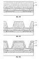
- FIGS. 17A-17K are cross-sectional views depicting an embodiment of the manufacturing of an interferometric modulator utilizing a mechanically isolated movable reflective layer and guide posts.
- FIGS. 18A-18C are cross-sectional views depicting an alternative embodiment of manufacturing steps for the manufacture of an interferometric modulator utilizing a mechanically isolated movable reflective layer and guide posts.
- the embodiments may be implemented in or associated with a variety of electronic devices such as, but not limited to, mobile telephones, wireless devices, personal data assistants (PDAs), hand-held or portable computers, GPS receivers/navigators, cameras, MP3 players, camcorders, game consoles, wrist watches, clocks, calculators, television monitors, flat panel displays, computer monitors, auto displays (e.g., odometer display, etc.), cockpit controls and/or displays, display of camera views (e.g., display of a rear view camera in a vehicle), electronic photographs, electronic billboards or signs, projectors, architectural structures, packaging, and aesthetic structures (e.g., display of images on a piece of jewelry).
- MEMS devices of similar structure to those described herein can also be used in non-display applications such as in electronic switching devices.
- FIG. 1 One interferometric modulator display embodiment comprising an interferometric MEMS display element is illustrated in FIG. 1 .
- the pixels are in either a bright or dark state.
- the display element In the bright (“on” or “open”) state, the display element reflects a large portion of incident visible light to a user.
- the dark (“off” or “closed”) state When in the dark (“off” or “closed”) state, the display element reflects little incident visible light to the user.
- the light reflectance properties of the “on” and “off” states may be reversed.
- MEMS pixels can be configured to reflect predominantly at selected colors, allowing for a color display in addition to black and white.
- FIG. 1 is an isometric view depicting two adjacent pixels in a series of pixels of a visual display, wherein each pixel comprises a MEMS interferometric modulator.
- an interferometric modulator display comprises a row/column array of these interferometric modulators.
- Each interferometric modulator includes a pair of reflective layers positioned at a variable and controllable distance from each other to form a resonant optical cavity with at least one variable dimension.
- one of the reflective layers may be moved between two positions. In the first position, referred to herein as the relaxed position, the movable reflective layer is positioned at a relatively large distance from a fixed partially reflective layer.
- the movable reflective layer In the second position, referred to herein as the actuated position, the movable reflective layer is positioned more closely adjacent to the partially reflective layer. Incident light that reflects from the two layers interferes constructively or destructively depending on the position of the movable reflective layer, producing either an overall reflective or non-reflective state for each pixel.
- the depicted portion of the pixel array in FIG. 1 includes two adjacent interferometric modulators 12 a and 12 b .
- a movable reflective layer 14 a is illustrated in a relaxed position at a predetermined distance from an optical stack 16 a , which includes a partially reflective layer.
- the movable reflective layer 14 b is illustrated in an actuated position adjacent to the optical stack 16 b.
- optical stack 16 typically comprise several fused layers, which can include an electrode layer, such as indium tin oxide (ITO), a partially reflective layer, such as chromium, and a transparent dielectric.
- ITO indium tin oxide
- the optical stack 16 is thus electrically conductive, partially transparent and partially reflective, and may be fabricated, for example, by depositing one or more of the above layers onto a transparent substrate 20 .
- the partially reflective layer can be formed from a variety of materials that are partially reflective such as various metals, semiconductors, and dielectrics.
- the partially reflective layer can be formed of one or more layers of materials, and each of the layers can be formed of a single material or a combination of materials.
- the layers of the optical stack are patterned into parallel strips, and may form row electrodes in a display device as described further below.
- the movable reflective layers 14 a , 14 b may be formed as a series of parallel strips of a deposited metal layer or layers (orthogonal to the row electrodes of 16 a , 16 b ) deposited on top of posts 18 and an intervening sacrificial material deposited between the posts 18 . When the sacrificial material is etched away, the movable reflective layers 14 a , 14 b are separated from the optical stacks 16 a , 16 b by a defined gap 19 .
- a highly conductive and reflective material such as aluminum may be used for the reflective layers 14 , and these strips may form column electrodes in a display device.
- the cavity 19 remains between the movable reflective layer 14 a and optical stack 16 a , with the movable reflective layer 14 a in a mechanically relaxed state, as illustrated by the pixel 12 a in FIG. 1 .
- a potential difference is applied to a selected row and column, the capacitor formed at the intersection of the row and column electrodes at the corresponding pixel becomes charged, and electrostatic forces pull the electrodes together.
- the movable reflective layer 14 is deformed and is forced against the optical stack 16 .
- a dielectric layer within the optical stack 16 may prevent shorting and control the separation distance between layers 14 and 16 , as illustrated by pixel 12 b on the right in FIG. 1 .
- the behavior is the same regardless of the polarity of the applied potential difference. In this way, row/column actuation that can control the reflective vs. non-reflective pixel states is analogous in many ways to that used in conventional LCD and other display technologies.
- FIGS. 2 through 5 illustrate one exemplary process and system for using an array of interferometric modulators according to FIG. 1 in a display application.
- FIG. 2 is a system block diagram illustrating one embodiment of an electronic device that may incorporate aspects of an interferometric modulator display.
- the electronic device includes a processor 21 which may be any general purpose single- or multi-chip microprocessor such as an ARM, Pentium®, Pentium II®, Pentium III®, Pentium IV®, Pentium® Pro, an 8051, a MIPS®, a Power PC®, an ALPHA®, or any special purpose microprocessor such as a digital signal processor, microcontroller, or a programmable gate array.
- the processor 21 may be configured to execute one or more software modules.
- the processor may be configured to execute one or more software applications, including a web browser, a telephone application, an email program, or any other software application.
- the processor 21 is also configured to communicate with an array driver 22 .
- the array driver 22 includes a row driver circuit 24 and a column driver circuit 26 that provide signals to a display array or panel 30 .
- the cross section of the array illustrated in FIG. 1 is shown by the lines 1 - 1 in FIG. 2 .
- the row/column actuation protocol may take advantage of a hysteresis property of these devices illustrated in FIG. 3 . It may require, for example, a 10 volt potential difference to cause a movable layer to deform from the relaxed state to the actuated state. However, when the voltage is reduced from that value, the movable layer maintains its state as the voltage drops back below 10 volts.
- the movable layer does not relax completely until the voltage drops below 2 volts.
- There is thus a range of voltage, about 3 to 7 V in the example illustrated in FIG. 3 where there exists a window of applied voltage within which the device is stable in either the relaxed or actuated state. This is referred to herein as the “hysteresis window” or “stability window.”
- hysteresis window or “stability window.”
- the row/column actuation protocol can be designed such that during row strobing, pixels in the strobed row that are to be actuated are exposed to a voltage difference of about 10 volts, and pixels that are to be relaxed are exposed to a voltage difference of close to zero volts. After the strobe, the pixels are exposed to a steady state voltage difference of about 5 volts such that they remain in whatever state the row strobe put them in. After being written, each pixel sees a potential difference within the “stability window” of 3-7 volts in this example. This feature makes the pixel design illustrated in FIG. 1 stable under the same applied voltage conditions in either an actuated or relaxed pre-existing state.
- each pixel of the interferometric modulator is essentially a capacitor formed by the fixed and moving reflective layers, this stable state can be held at a voltage within the hysteresis window with almost no power dissipation. Essentially no current flows into the pixel if the applied potential is fixed.
- a display frame may be created by asserting the set of column electrodes in accordance with the desired set of actuated pixels in the first row.
- a row pulse is then applied to the row 1 electrode, actuating the pixels corresponding to the asserted column lines.
- the asserted set of column electrodes is then changed to correspond to the desired set of actuated pixels in the second row.
- a pulse is then applied to the row 2 electrode, actuating the appropriate pixels in row 2 in accordance with the asserted column electrodes.
- the row 1 pixels are unaffected by the row 2 pulse, and remain in the state they were set to during the row 1 pulse. This may be repeated for the entire series of rows in a sequential fashion to produce the frame.
- the frames are refreshed and/or updated with new display data by continually repeating this process at some desired number of frames per second.
- protocols for driving row and column electrodes of pixel arrays to produce display frames are also well known and may be used in conjunction with the present invention.
- FIGS. 4 and 5 illustrate one possible actuation protocol for creating a display frame on the 3 ⁇ 3 array of FIG. 2 .
- FIG. 4 illustrates a possible set of column and row voltage levels that may be used for pixels exhibiting the hysteresis curves of FIG. 3 .
- actuating a pixel involves setting the appropriate column to ⁇ V bias , and the appropriate row to + ⁇ V, which may correspond to ⁇ 5 volts and +5 volts respectively. Relaxing the pixel is accomplished by setting the appropriate column to +V bias , and the appropriate row to the same + ⁇ V, producing a zero volt potential difference across the pixel.
- the pixels are stable in whatever state they were originally in, regardless of whether the column is at +V bias , or ⁇ V bias .
- voltages of opposite polarity than those described above can be used, e.g., actuating a pixel can involve setting the appropriate column to +V bias , and the appropriate row to ⁇ V.
- releasing the pixel is accomplished by setting the appropriate column to ⁇ V bias , and the appropriate row to the same ⁇ V, producing a zero volt potential difference across the pixel.
- FIG. 5B is a timing diagram showing a series of row and column signals applied to the 3 ⁇ 3 array of FIG. 2 which will result in the display arrangement illustrated in FIG. 5A , where actuated pixels are non-reflective.
- the pixels Prior to writing the frame illustrated in FIG. 5A , the pixels can be in any state, and in this example, all the rows are at 0 volts, and all the columns are at +5 volts. With these applied voltages, all pixels are stable in their existing actuated or relaxed states.
- pixels (1,1), (1,2), (2,2), (3,2) and (3,3) are actuated.
- columns 1 and 2 are set to ⁇ 5 volts, and column 3 is set to +5 volts. This does not change the state of any pixels, because all the pixels remain in the 3-7 volt stability window.
- Row 1 is then strobed with a pulse that goes from 0, up to 5 volts, and back to zero. This actuates the (1,1) and (1,2) pixels and relaxes the (1,3) pixel. No other pixels in the array are affected.
- column 2 is set to ⁇ 5 volts
- columns 1 and 3 are set to +5 volts.
- Row 3 is similarly set by setting columns 2 and 3 to ⁇ 5 volts, and column 1 to +5 volts.
- the row 3 strobe sets the row 3 pixels as shown in FIG. 5A .
- the row potentials are zero, and the column potentials can remain at either +5 or ⁇ 5 volts, and the display is then stable in the arrangement of FIG. 5A . It will be appreciated that the same procedure can be employed for arrays of dozens or hundreds of rows and columns.
- FIGS. 6A and 6B are system block diagrams illustrating an embodiment of a display device 40 that may incorporate interferometric modulator elements according to any of the structures described herein.
- the display device 40 can be, for example, a cellular or mobile telephone.
- the same components of display device 40 or slight variations thereof are also illustrative of various types of display devices such as televisions and portable media players.
- the display device 40 includes a housing 41 , a display 30 , an antenna 43 , a speaker 44 , an input device 48 , and a microphone 46 .
- the housing 41 is generally formed from any of a variety of manufacturing processes as are well known to those of skill in the art, including injection molding, and vacuum forming.
- the housing 41 may be made from any of a variety of materials, including but not limited to plastic, metal, glass, rubber, and ceramic, or a combination thereof.
- the housing 41 includes removable portions (not shown) that may be interchanged with other removable portions of different color, or containing different logos, pictures, or symbols.
- the display 30 of exemplary display device 40 may be any of a variety of displays, including a bi-stable display, as described herein.
- the display 30 includes a flat-panel display, such as plasma, EL, OLED, STN LCD, or TFT LCD as described above, or a non-flat-panel display, such as a CRT or other tube device, as is well known to those of skill in the art.
- the display 30 includes an interferometric modulator display, as described herein.
- the components of one embodiment of exemplary display device 40 are schematically illustrated in FIG. 6B .
- the illustrated exemplary display device 40 includes a housing 41 and can include additional components at least partially enclosed therein.
- the exemplary display device 40 includes a network interface 27 that includes an antenna 43 which is coupled to a transceiver 47 .
- the transceiver 47 is connected to a processor 21 , which is connected to conditioning hardware 52 .
- the conditioning hardware 52 may be configured to condition a signal (e.g. filter a signal).
- the conditioning hardware 52 is connected to a speaker 45 and a microphone 46 .
- the processor 21 is also connected to an input device 48 and a driver controller 29 .
- the driver controller 29 is coupled to a frame buffer 28 , and to an array driver 22 , which in turn is coupled to a display array 30 .
- a power supply 50 provides power to all components as required by the particular exemplary display device 40 design.
- the network interface 27 includes the antenna 43 and the transceiver 47 so that the exemplary display device 40 can communicate with one ore more devices over a network. In one embodiment the network interface 27 may also have some processing capabilities to relieve requirements of the processor 21 .
- the antenna 43 is any antenna known to those of skill in the art for transmitting and receiving signals. In one embodiment, the antenna transmits and receives RF signals according to the IEEE 802.11 standard, including IEEE 802.11(a), (b), or (g). In another embodiment, the antenna transmits and receives RF signals according to the BLUETOOTH standard. In the case of a cellular telephone, the antenna is designed to receive CDMA, GSM, AMPS or other known signals that are used to communicate within a wireless cell phone network.
- the transceiver 47 pre-processes the signals received from the antenna 43 so that they may be received by and further manipulated by the processor 21 .
- the transceiver 47 also processes signals received from the processor 21 so that they may be transmitted from the exemplary display device 40 via the antenna 43 .
- the transceiver 47 can be replaced by a receiver.
- network interface 27 can be replaced by an image source, which can store or generate image data to be sent to the processor 21 .
- the image source can be a digital video disc (DVD) or a hard-disc drive that contains image data, or a software module that generates image data.
- Processor 21 generally controls the overall operation of the exemplary display device 40 .
- the processor 21 receives data, such as compressed image data from the network interface 27 or an image source, and processes the data into raw image data or into a format that is readily processed into raw image data.
- the processor 21 then sends the processed data to the driver controller 29 or to frame buffer 28 for storage.
- Raw data typically refers to the information that identifies the image characteristics at each location within an image. For example, such image characteristics can include color, saturation, and gray-scale level.
- the processor 21 includes a microcontroller, CPU, or logic unit to control operation of the exemplary display device 40 .
- Conditioning hardware 52 generally includes amplifiers and filters for transmitting signals to the speaker 45 , and for receiving signals from the microphone 46 .
- Conditioning hardware 52 may be discrete components within the exemplary display device 40 , or may be incorporated within the processor 21 or other components.
- the driver controller 29 takes the raw image data generated by the processor 21 either directly from the processor 21 or from the frame buffer 28 and reformats the raw image data appropriately for high speed transmission to the array driver 22 . Specifically, the driver controller 29 reformats the raw image data into a data flow having a raster-like format, such that it has a time order suitable for scanning across the display array 30 . Then the driver controller 29 sends the formatted information to the array driver 22 .
- a driver controller 29 such as a LCD controller, is often associated with the system processor 21 as a stand-alone Integrated Circuit (IC), such controllers may be implemented in many ways. They may be embedded in the processor 21 as hardware, embedded in the processor 21 as software, or fully integrated in hardware with the array driver 22 .
- the array driver 22 receives the formatted information from the driver controller 29 and reformats the video data into a parallel set of waveforms that are applied many times per second to the hundreds and sometimes thousands of leads coming from the display's x-y matrix of pixels.
- driver controller 29 is a conventional display controller or a bi-stable display controller (e.g., an interferometric modulator controller).
- array driver 22 is a conventional driver or a bi-stable display driver (e.g., an interferometric modulator display).
- a driver controller 29 is integrated with the array driver 22 .
- display array 30 is a typical display array or a bi-stable display array (e.g., a display including an array of interferometric modulators).
- the input device 48 allows a user to control the operation of the exemplary display device 40 .
- input device 48 includes a keypad, such as a QWERTY keyboard or a telephone keypad, a button, a switch, a touch-sensitive screen, a pressure- or heat-sensitive membrane.
- the microphone 46 is an input device for the exemplary display device 40 . When the microphone 46 is used to input data to the device, voice commands may be provided by a user for controlling operations of the exemplary display device 40 .
- Power supply 50 can include a variety of energy storage devices as are well known in the art.
- power supply 50 is a rechargeable battery, such as a nickel-cadmium battery or a lithium ion battery.
- power supply 50 is a renewable energy source, a capacitor, or a solar cell, including a plastic solar cell, and solar-cell paint.
- power supply 50 is configured to receive power from a wall outlet.
- control programmability resides, as described above, in a driver controller which can be located in several places in the electronic display system. In some cases control programmability resides in the array driver 22 . Those of skill in the art will recognize that the above-described optimization may be implemented in any number of hardware and/or software components and in various configurations.
- FIGS. 7A-7E illustrate five different embodiments of interferometric modulators operating essentially under the same principles as the one described in connection with FIGS. 1-5B .
- FIG. 7A is a cross section of the embodiment of FIG. 1 , where a strip of metal material 14 is deposited on orthogonally extending supports 18 .
- the moveable reflective layer 14 is attached to supports at the corners only, on tethers 32 .
- the moveable reflective layer 14 is suspended from a deformable layer 34 , which may comprise a flexible metal.
- the deformable layer 34 connects, directly or indirectly, to the substrate 20 around the perimeter of the deformable layer 34 . These connections are herein referred to as support posts.
- FIG. 7D has support post plugs 42 upon which the deformable layer 34 rests.
- the movable reflective layer 14 remains suspended over the cavity, as in FIGS. 7A-7C , but the deformable layer 34 does not form the support posts by filling holes between the deformable layer 34 and the optical stack 16 . Rather, the support posts are formed of a planarization material, which is used to form support post plugs 42 .
- the embodiment illustrated in FIG. 7E is based on the embodiment shown in FIG. 7D , but may also be adapted to work with any of the embodiments illustrated in FIGS. 7A-7C as well as additional embodiments not shown. In the embodiment shown in FIG. 7E , an extra layer of metal or other conductive material has been used to form a bus structure 44 . This allows signal routing along the back of the interferometric modulators, eliminating a number of electrodes that may otherwise have had to be formed on the substrate 20 .
- the interferometric modulators function as direct-view devices, in which images are viewed from the front side of the transparent substrate 20 , the side opposite to that upon which the modulator is arranged.
- the reflective layer 14 optically shields the portions of the interferometric modulator on the side of the reflective layer opposite the substrate 20 , including the deformable layer 34 . This allows the shielded areas to be configured and operated upon without negatively affecting the image quality.
- Such shielding allows the bus structure 44 in FIG. 7E , which provides the ability to separate the optical properties of the modulator from the electromechanical properties of the modulator, such as addressing and the movements that result from that addressing.
- This separable modulator architecture allows the structural design and materials used for the electromechanical aspects and the optical aspects of the modulator to be selected and to function independently of each other.
- the embodiments shown in FIGS. 7C-7E have additional benefits deriving from the decoupling of the optical properties of the reflective layer 14 from its mechanical properties, which are carried out by the deformable layer 34 .
- This allows the structural design and materials used for the reflective layer 14 to be optimized with respect to the optical properties, and the structural design and materials used for the deformable layer 34 to be optimized with respect to desired mechanical properties.
- a movable mirror is coupled to a mechanical membrane such that mechanical restoring forces are built in to the device.
- the mechanical membrane is deflected from its stationary or quiescent position by an applied voltage and resulting electrostatic attraction. In the absence of the applied voltage, the mechanical restoring forces cause the membrane to revert to a position that is a pre-selected distance from the stationary reflective layer.
- restoring forces are bulk forces, which do not scale favorably with the shrinking of device size. This restricts the size of the mirror that can be used in these types of interferometric modulators.
- the restriction on mirror size can result in a lower fill factor (i.e., the ratio of active pixel area to non-active pixel area) and lower contrast ratio.
- the materials used for the mechanical membrane may be different from those used for the mirror, which can cause undesirable tilt and/or curvature in the mirror.
- a mismatch in coefficient of thermal expansion between the mirror and the mechanical membrane can affect thermal stability of the device, causing mirror curvature.
- stress relaxation in the mechanical membrane due to aging and other effects can degrade the restoring forces and create image retention issues in the interferometric modulator.
- interferometric modulators are provided that comprise a mirror that is mechanically isolated from the rest of the interferometric modulator structure.
- FIG. 8 One such embodiment comprising an interferometric MEMS display element is illustrated in FIG. 8 .
- the pixels may be in either a bright or dark state. In the bright (“on” or “open”) state, the display element reflects a large portion of incident visible light to a user. When in the dark (“off” or “closed”) state, the display element reflects little incident visible light to the user.
- the light reflectance properties of the “on” and “off” states may be reversed.
- MEMS pixels can also be configured to reflect predominantly at selected colors, allowing for a color display in addition to black and white. MEMS pixels can further be configured to provide analog operation in which the light reflectance properties may change between dark, color of varying wavelength, and bright states.
- FIG. 8 is an isometric view depicting an embodiment of two adjacent pixels in a series of pixels of a visual display (only two of the pixels are shown for the sake of clarity), wherein each pixel comprises a MEMS interferometric modulator having a mirror 14 that is mechanically isolated (floating) from the rest of the interferometric modulator structure.
- Mirror 14 is analogous to the reflective layer 14 illustrated in FIGS. 7A-7D .
- an interferometric modulator display comprises an array of these interferometric modulators arranged in rows and columns.
- Each interferometric modulator includes a pair of reflective layers positioned at a controlled variable distance from each other to form a resonant optical cavity with at least one variable dimension.
- one of the reflective layers may be moved between two positions.
- the movable reflective layer In the first position, referred to herein as the down position, the movable reflective layer is positioned at a relatively large distance from a fixed partially reflective layer.
- the second position In the second position, referred to herein as the up position, the movable reflective layer is positioned more closely adjacent to the partially reflective layer. Incident light that reflects from the two layers can interfere constructively or destructively depending on the position of the movable reflective layer, producing a selectable reflective or non-reflective state for each pixel.
- the depicted portion of the pixel array in FIG. 8 includes two adjacent interferometric modulators 12 a and 12 b .
- a movable reflective layer 14 a is illustrated in the down position at a predetermined distance from an optical stack 16 a , which includes a partially reflective layer (not shown for clarity).
- the distance of the movable reflective layer 14 a from the optical stack 16 a is determined by the location of a bottom electrode 17 a with respect to the optical stack 16 a .
- the distance between the optical stack 16 a and the movable reflective layer 14 a may be on the order of hundreds of angstroms.
- the movable reflective layer 14 b is illustrated in the up position, where the movable reflective layer 14 b is adjacent to the optical stack 16 b (i.e., the gap or distance between the movable reflective layer 14 b and the optical stack 16 b is less than 300 angstroms).
- the movable reflective layers 14 a and 14 b may be mechanically isolated from the optical stacks 16 a and 16 b and the bottom electrodes 17 a and 17 b .
- mechanically isolated it is meant that the movable reflective layers 14 experience no substantial restoring forces in a direction opposing a direction of movement due to contact with other structures in the interferometric modulators (e.g., due to mechanical tethers or springs).
- the movable reflective layers 14 may be constructed from any suitable reflective material such as various metals (e.g., aluminum, nickel, gold) or a dielectric stack (e.g., dielectric mirror).
- the movable reflective layers 14 are aluminum.
- the movable reflective layer 14 comprises multiple layers sandwiched together.
- optical stack 16 typically comprise several fused layers, which can include an electrode layer (e.g., a top electrode), such as indium tin oxide (ITO), a partially reflective layer such as chromium, and a transparent dielectric.
- the optical stack 16 thus comprises an electrically conductive portion, is partially transparent and partially reflective, and may be fabricated, for example, by depositing one or more of the above layers onto a transparent substrate 20 .
- the partially reflective layer can be formed from a variety of materials that are partially reflective such as various metals, semiconductors, and dielectrics.
- the partially reflective layer can be formed of one or more layers of materials, and each of the layers can be formed of a single material or a combination of materials.
- the dielectric layer in the optical stack serves to electrically insulate the movable reflective layers 14 from the conductive portions of the optical stacks 16 as well as define the position of the movable reflective layers 14 when the interferometric modulator is in the up state.
- a dielectric layer may be deposited on a surface of the movable reflective layer 14 facing the optical stack 16 in order to electrically insulate the movable reflective layer 14 from the electrode in the optical stack 16 when in the up state.
- the bottom electrodes 17 a and 17 b may be constructed of any conductive material such as metal (e.g. aluminum, silver, nickel, gold) or indium tin oxide (ITO).
- a dielectric layer (not shown) is included to insulate the bottom electrodes 17 from the movable reflective layers 14 when the interferometric modulator is in the down state.
- the bottom electrodes 17 and dielectric layer combination are rigid enough such that they do not deform under the electrical forces applied during pixel driving.
- the bottom electrodes 17 are supported by a second substrate (not shown) spaced from the substrate 20 (i.e., the second substrate is located on the bottom of the interferometric modulators depicted in FIG. 1 ).
- a dielectric layer may be deposited on the surface of the movable reflective layer 14 facing the bottom electrode 17 in order to electrically insulate the movable reflective layer 14 from the bottom electrode 17 .
- the movable reflective layers 14 may be moved between the up state and the down state using electrostatic forces provided between the optical stack 16 and the bottom electrodes 17 .
- the electrostatic forces may be induced by applying voltages to the optical stack 16 and bottom electrodes 17 .
- charge is transferred into or out of the movable reflective layers 14 to create a desired potential difference between the movable reflective layers 14 and the optical stack 16 and/or the bottom electrodes 17 .
- the charge transfer element may be any suitable structure for changing the charge of the movable reflective layers 14 such as an electrical coupling to a driving circuit (e.g.
- charge is permanently embedded in the movable reflective layer during manufacturing.
- a potential difference is generated between an optical stack 16 and a movable reflective layer 14
- the movable reflective layer 14 moves towards the optical stack 16 until it is in an up position (e.g. as depicted by the interferometric modulator 12 b in FIG. 8 ).
- the movable reflective layer 14 moves towards the bottom electrode 17 until it is in a down position (e.g.
- the interferometric modulator 12 a in FIG. 8 When no voltage is applied to either the optical stack 16 or the bottom electrode 17 , the movable reflective layer 14 will remain in its current state (either up or down), held in place by adhesive forces. Thus, a display utilizing interferometric modulators according to FIG. 8 can retain an image without any power supplied to it.
- the movable reflective layer 14 is also magnetized. Magnetic layers may then be included in the bottom electrode 17 and optical stack 16 to provide further holding forces when the movable reflective layer 14 is an up or down state.
- magnetic structures may optionally be included at various other locations in the interferometric modulator to magnetically guide the movable reflective layer 14 while it is moving. For example, magnetic structures on the periphery of the interferometric modulator may be used to limit lateral movement of the movable reflective layer 14 .
- the movable reflective layer 14 can be electrically insulated from the optical stack 16 and the bottom electrode 17 by intervening dielectric layers deposited either on the optical stack 16 and bottom electrode 17 and/or on the movable reflective layer 14 itself. In some embodiments, the movable reflective layer 14 may also be electrically isolated from the optical stack 16 and bottom electrodes 17 through external circuitry, such as a diode, that prevents current flow.
- the potential of the movable reflective layers 14 may be uncontrolled at all times, may be controlled only when in the up or down positions, or may be controlled in an analog fashion at all positions of movement between the fully up state and the fully down state. In one embodiment, the movable reflective layers 14 remain electrically floating at some arbitrary voltage. However, the arbitrary voltage is not necessarily predictable and may change over the lifetime of the display. Alternatively, the potential of the movable reflective layers 14 may be controlled only when in the up or down states by providing charge transfer elements (e.g. electrical contacts) that can supply charge to the movable reflective layers 14 when in these states.
- charge transfer elements e.g. electrical contacts
- the electrical contacts are always connected to ground (i.e., grounding planes are provided that contact the movable reflective layers 14 when in the up or down state).
- the grounding planes are conductive (e.g., metal) layers overlapping a portion of the dielectric layers deposited on the optical stack 16 and bottom electrode 17 .
- the movable reflective layer 14 When the movable reflective layer 14 is in a down or up state, it will contact both the respective dielectric layer and the grounding plane.
- grounding planes are described in more detail below with respect to FIGS. 17A-17K .
- the potential of the movable reflective layers 14 are also controlled during movement by utilizing conductive guides that contact the movable reflective layers 14 or by providing a thin flexible tether electrically coupled to the movable reflective layers 14 at all times.
- any tether used is flexible enough that it doesn't supply any substantial mechanical force to the movable reflective layers.
- tethers may be made from materials with low stress and small Young's modulus.
- a layer of thin Al e.g., less than about 50 nm
- Such layers may also be used to form the reflective material in the movable reflective layer.
- the same deposition step may be used to form the movable reflective layer and the tethers.
- the width of the tether is less than 10 ⁇ m.
- tethers are attached between the movable reflective layer and a guide post. In one embodiment, the location of attachment to the guide post is approximately in the middle of the guide post in order to equally minimize mechanical influence for both top and bottom positions of the movable reflective layer.
- the top and bottom electrodes (the optical stack 16 and the bottom electrode 17 ) for each interferometric modulator are divided into two or more sub-electrodes that may be individually driven. Such an arrangement allows tilt to be induced into the movable reflective layer 14 .
- the top electrode of optical stack 16 is divided into left and right halves and the bottom electrode 17 is divided into left and right halves. If the same non-ground potential is driven on the top left and right sub-electrodes, then the movable reflective layer 14 will be drawn to an up state (e.g. a dark state).
- the movable reflective layer 14 will be drawn to a down state (e.g., a bright state having the color determined by the reflective layer spacing). If however, the same non-ground potentials are driven to the top left and bottom right sub-electrodes while top right and bottom left sub-electrodes are held at ground potential, then the movable reflective layer 14 will tilt with the left half attracted to an up state and the right half attracted to a down state. Such a tilted movable reflective layer 14 may cause the interferometric modulator to reflect a virtual white state due to the spectral width of the reflected light.
- a tilted movable reflective layer 14 may cause the interferometric modulator to reflect a virtual white state due to the spectral width of the reflected light.
- this type of interferometric modulator can provide three display states, a dark state, a bright color state, and a bright white state.
- MEMS devices having a mechanically isolated electrically attractable member may be used in virtually any application where a mechanical membrane might otherwise be used.
- MEMS structures having two electrodes with an intermediate electrically attractable member may be used in electrical switching applications, optical switching applications, piezoelectric applications, and sensor applications.
- an electromechanical analysis was conducted to model the electrostatic potentials and forces involved in moving the movable reflective layer 14 from one state to another.
- the potential of the movable reflective layer 14 was assumed to be zero prior to moving and to be electrically floating during motion. In practice, these characteristics can be achieved by using the grounding planes described above to contact the movable reflective layer 14 when in the up or down states.
- the potential difference between the movable reflective layer 14 and the electrode to which it is to move must be greater than any forces holding the movable reflective layer 14 in its current state.
- the forces holding the movable reflective layer 14 and the electrode may include adhesive forces and/or magnetic forces.
- Empirical tests have shown that for a mirror having an area of 70 ⁇ 20 ⁇ m 2 , adhesive forces between an aluminum mirror and a dielectric layer are about 10 ⁇ N. Thus, 10 ⁇ N was used as the minimum required initial electrostatic force.
- the electrostatic force may be given by:
- V top is the potential of the top electrode (i.e., the optical stack 16 )
- V mirror is the potential of the movable reflective layer 14
- V bottom is the potential of the bottom electrode 17 . Since the potential between the bottom electrode 17 and the movable reflective layer 14 is sufficient to overcome adhesive forces, the movable reflective layer 14 releases from its static position against the bottom electrode 17 and becomes electrically isolated (i.e., its charge will remain constant).
- the charge on the movable reflective layer 14 may be given by:
- the voltage as a function of movable reflective layer 14 displacement x is given by:
- V mirror - bottom Q ⁇ ( d - x ) ⁇ 0 ⁇ A e ( 3 )
- the electrostatic force supplied to the movable reflective layer 14 by the bottom electrode 17 as a function of displacement is given by:
- FIG. 9 is a graph depicting, in one embodiment, the voltage between the movable reflective layer 14 and the top and bottom electrodes, respectively, during actuation.
- the x-axis of the graph is the distance between the movable reflective layer 14 and the bottom electrode 17 .
- the voltages change from right to left.
- the graph demonstrates that the voltage between the movable reflective layer 14 and the bottom electrode 17 increases linearly while the voltage between the movable reflective layer 14 and the top electrode decreases linearly.
- FIG. 10 is a graph depicting, in one embodiment, the independent forces exerted on the movable reflective layer 14 by the top electrode and the bottom electrode, as well as the net force exerted on the movable reflective layer 14 by the two electrodes.
- the sign convention is such that positive forces are in the upward direction. It can be seen that the net force remains negative throughout the motion of the movable reflective layer 14 from top to bottom (i.e., from right to left in the graph).
- the interferometric modulators described above include guides to constrain lateral movement of the movable reflective layer 14 .
- FIG. 11 is a perspective view of one interferometric modulator according to FIG. 8 comprising a top electrode 16 , a bottom electrode 17 , and a movable reflective layer 14 .
- the interferometric modulator is viewed upside down relative to the view presented in FIG. 8 in order to illustrate black masks 104 a and 104 b described below.
- Two posts 100 a and 100 b (referred to collectively as posts 100 ) extend between the top 16 and bottom 17 electrodes.
- the posts 100 a and 100 b extend through two apertures 102 a and 102 b (referred to collectively as apertures 102 ) formed in the movable reflective layer 14 .
- the apertures 102 a and 102 b are larger than the width of the posts 100 a and 100 b so that the movable reflective layer 14 can slide freely up and down over the posts 100 a and 100 b .
- the posts 100 prevent significant lateral or rotational motion of the movable reflective layer 14 while it is being actuated.
- the posts 100 can structurally support the bottom electrode 17 (e.g., where the bottom electrode 17 depends upon the substrate 20 for structural support rather than being formed on another “bottom” substrate).
- the posts 100 or portions thereof are formed of conductive material such that when the movable reflective layer 14 contacts the posts 100 , the potential of the movable reflective layer 14 can be controlled through an electrical connection between the posts 100 and a driving circuit.
- guides positioned along the edges of each interferometric modulator which may take the form of posts or walls, may also constrain the lateral and/or rotational motion of the movable reflective layer 14 .
- any number of posts and post locations may be considered.
- guides include magnetic structures to constrain lateral movement through the use of magnetic forces.
- the top electrode 16 i.e., the optical stack
- the posts 100 would be visible to a user, thereby decreasing the fill factor and contrast ratio of the display.
- black masks 104 a and 104 b are formed between the posts 100 a and 100 b and the substrate 20 to reduce their visual impact.
- the black masks 104 a and 104 b are formed on the surface of substrate 20 opposite the posts 100 a and 100 b .
- the black masks 104 are made large enough to hide the posts 100 , the apertures 102 in the movable reflective layer 14 , and grounding planes at the base of the posts used to electrically contact the movable reflective layer 14 .
- the posts 100 are 6 ⁇ m ⁇ 6 ⁇ m
- the apertures 102 are 10 ⁇ m ⁇ 10 ⁇ m
- the black masks 104 are 20 ⁇ m ⁇ 20 ⁇ m.
- FIG. 12 is a top-down view of an array of interferometric modulators 12 depicting the black masks 104 on the substrate and the footprint of the optical stack 16 in one embodiment.
- the array may be characterized by interferometric modulator pitch (i.e., the distance from the start of one interferometric modulator to the start of an adjacent interferometric modulator) and the dimensions of the reflective surfaces (e.g. optical stack and movable reflective layer).
- the difference in interferometric modulator pitch and reflective surface size is due to: 1) the built in space between adjacent reflective surfaces to reduce the possibility of mechanical or electrical effects caused by adjacent interferometric modulators and 2) photo and etch biases. Based on this information, fill factors can be determined for various display layouts.
- pixel pitch would be 222 ⁇ m.
- Factoring for photo and etch bias (e.g. 1 ⁇ m on each edge) and functional spacing (e.g. 4 ⁇ m) this pitch could be achieved using 216 ⁇ m ⁇ 216 ⁇ m optical stack/movable reflective layer structures. Assuming black mask areas of 20 ⁇ m ⁇ 20 ⁇ m and considering the non-display area in between pixels, a fill factor of 94% can be achieved.
- An advantage of some embodiments of the interferometric modulator with mechanically isolated movable reflective layer 14 is that fill factors may be increased in comparison to conventional interferometric modulators utilizing mechanical supports for the movable mirror. Conventional designs have fill factors that are typically between 65%-75%.
- FIG. 13 Fill factors for various interferometric modulator pitches and display types are depicted in the graph in FIG. 13 .
- the various color displays may be constructed by having each pixel comprise several interferometric modulators (i.e., sub-pixels). Different color sub-pixels may be constructed by varying the maximum distance accessible between the movable reflective layer and the optical stack. In some embodiments, color depth may be increased by having multiple sub-pixels of the same color in each pixel.
- FIG. 13 depicts fill factors for a monochrome design, RGB primary color designs having 1 bit per color (3 sub-pixels), 2 bit per color (6 sub-pixels), or 3 bit per color (9 sub-pixels), and a 4 primary color design.
- the fill factor for each case was calculated using conservative design rules for mirror spacing and black mask regions to hide the post structure.
- the black mask regions occupy two 20 ⁇ m ⁇ 20 ⁇ m squares near the center of each sub-pixel.
- the space between the mirrors are defined by a 4 um photolithography space and a 1 ⁇ m CD loss per side.
- a display including an array of interferometric modulators as described above is driven using an active-matrix driving scheme.
- each interferometric modulator is connected to a switch circuit for determining upon an update scan whether the interferometric modulator should be actuated and if so, whether the actuation should be to the up state or down state.
- the switch circuit for each interferometric modulator is formed in the proximity of the interferometric modulator at the same time as the interferometric modulator is manufactured, for example in similar fashion to that described in co-pending and commonly-assigned U.S. application Ser. No. 11/331,705, filed Jan. 13, 2006.
- an array of switch circuits may be formed on the substrate adjacent to each interferometric modulator.
- the active switch elements of the array can be formed below, above or in the same layers as the interferometric modulator. Electrical connections between the switch elements and the interferometric modulator can be achieved by properly patterning conductive layers in the interferometric modulator.
- the switch circuit comprises one or more thin film transistors (TFTs). These TFTs may be constructed using techniques known to those of skill in the art.
- FIG. 14 is a schematic depicting one embodiment of an array of interferometric modulators 12 (each depicted isometrically as two parallel plates) and corresponding switch circuits 120 (not all interferometric modulators 12 and switch circuits 120 labeled, for clarity) coupled to an array driver 22 that is controlled by a processor 21 .
- each row of switch circuits 120 are connected to a single output from a scan driving circuit 122 that is part of the array driver 22 .
- each column of the switch circuits 120 are connected to a single output from a data driving circuit 124 that is also part of the array driver 22 .
- each switch circuit 120 may have a connection to a common driving voltage V dd .
- Each interferometric modulator 12 may also have a connection to a ground terminal for the purposes of grounding the movable reflective layer 14 in each interferometric modulator 12 .
- the image on the array may be updated row-by-row by sending a voltage pulse to the respective rows from the scan driving circuit 122 .
- Whether a pixel in the scanned row is actuated and whether actuation is to an up state or a down state is determined by voltages applied to each data driving circuit 124 output. For example, when no voltage is applied to the data driving lead for a particular pixel, the pixel does not change state.
- a voltage is applied, its magnitude or polarity may be used to determine whether actuation is to an up state or a down state.
- the array driver 22 communicates with a processor 21 , which may be any general purpose single- or multi-chip microprocessor such as an ARM, Pentium®, Pentium II®, Pentium III®, Pentium IV®, Pentium® Pro, an 8051, a MIPS®, a Power PC®, an ALPHA®, or any special purpose microprocessor such as a digital signal processor, microcontroller, or a programmable gate array.
- the processor 21 may be configured to execute one or more software modules.
- the processor may be configured to execute one or more software applications, including a web browser, a telephone application, an email program, or any other software application.
- FIG. 15 One embodiment of a switch circuit 120 as described above is illustrated in the circuit diagram in FIG. 15 .
- the scan lead 230 from the scan driving circuit 122 is connected to the gate terminal of a pass transistor 232 .
- the data lead 234 from the data driving circuit 124 is connected to the source terminal of the pass transistor 232 .
- the drain lead 236 of the pass transistor 232 is connected to the gates of two additional transistors, a top electrode transistor 238 and a bottom electrode transistor 240 that are respectively coupled to the interferometric modulator top electrode (of optical stack 16 ) and bottom electrode 17 .
- One of these transistors, such as the bottom electrode transistor 240 has reversed polarity such that only negative potentials applied to the gate permit current flow.
- the source terminals of the top and bottom electrode transistors 238 and 240 are connected to driving voltage source V dd .
- the drain lead 242 of the top electrode transistor 238 connects to the top electrode (i.e., the optical stack 16 ).
- the drain lead 244 of the bottom electrode transistor 240 connects to the bottom electrode 17 .
- the driving voltage V dd is applied to the top electrode of optical stack 16 , causing the movable reflective layer 14 of the interferometric modulator to actuate to an up state. If the data voltage has negative polarity, the driving voltage V dd is applied to the bottom electrode 17 , causing the movable reflective layer 14 of the interferometric modulator to actuate to a down state.
- the driving voltage V dd is applied to the bottom electrode 17 , causing the movable reflective layer 14 of the interferometric modulator to actuate to a down state.
- each interferometric modulator may be connected to a ground terminal 246 for grounding the movable reflective layer.
- the movable reflective layer 14 may be grounded at various times and by various means, including but not limited to, grounding plane contacts that contact the layer when it is in an up or down state, conductive guides (e.g. posts) that may contact the movable reflective layer 14 periodically during its actuation, and a conductive tether.
- interferometric modulators according to those described above may be considered as a three-terminal device with separate addressable electrodes for the top, bottom and movable reflective layers.
- FIG. 16 depicts a timing diagram for a three-terminal interferometric modulator in one embodiment.
- the grounding plane voltage remains 0 V at all times.
- a voltage pulse is applied to the top electrode of the optical stack 16 of the interferometric modulator. As shown in FIG. 16 , this first pulse causes the movable reflective layer 14 of the interferometric modulator to move to an up state.
- a subsequent pulse driven by the switching circuit 120 to the bottom electrode 17 causes the movable reflective layer 14 to move to a down state.
- the pulses driven to the top and bottom electrode terminals may also have reversed polarity and still result in the movable reflective layer 14 being actuated to an up or bottom state.
- the polarity of the driving voltage pulses is alternated for each sequential pulse (e.g., as shown in FIG. 16 ). This alternation of driving pulse polarity can be used to maintain an average neutral charge in the interferometric modulators.
- the polarity of the driving pulses may be alternated by periodically reversing the polarity of the driving voltage V dd supplied to each switching circuit.
- the layers of the optical stack 16 are patterned into individual rectangular electrodes (e.g. optical stacks 16 a and 16 b ), one for each interferometric modulator.
- the bottom electrodes 17 may be formed by patterning a bottom electrode layer into individual rectangular electrodes (e.g. bottom electrodes 17 a and 17 b ), one for each interferometric modulator.
- the bottom electrodes 17 may be supported by a series of posts by depositing the bottom electrode layer onto the top of the posts and an intervening sacrificial material deposited between the posts and over the movable reflective layers 14 .
- the bottom electrodes 17 are separated from the optical stack 16 by a gap 19 within which the movable reflective layers 14 are positioned.
- the bottom electrodes 17 are further supported by a second substrate deposited on top of the bottom electrodes 17 .
- the second substrate may be adhered to the first substrate 20 using an adhesive along the edges of the display.
- the interferometric modulators may be constructed using photolithographic techniques known to those of skill in the art. For example, in some embodiments, the interferometric modulators are manufactured through a series of deposition and etching steps. Each deposited layer of the material may be patterned by depositing a layer of photosensitive material such as photoresist which is then exposed to light in the desired pattern. The non-light exposed areas are removed using a suitable etchant followed by etching the now physically exposed layer below. Finally, the remaining photoresist is completely removed by a suitable etchant prior to deposition and patterning of further layers of material.
- photosensitive material such as photoresist
- FIGS. 17A-17K are cross-sectional views of a portion of an interferometric modulator depicting one method of manufacturing in one embodiment.
- the cross-section is through the portion of the interferometric modulator where black masks and posts are formed, such as depicted by cross-section 11 in FIG. 12 .
- black masks 300 are deposited onto transparent substrate 20 and patterned to hide the posts and grounding plane structures that will later be deposited on substrate 20 .
- a transparent dielectric layer 304 is deposited to isolate the black masks from the rest of the structure.
- the top electrode 306 (referred to as “top” because it is closest to the viewing side of the interferometric modulator although the viewing side is on the bottom of each of FIGS. 17A-K ) is deposited and patterned followed by deposition of another transparent dielectric layer 308 .
- the top electrode 306 may actually include several layers, including a transparent electrode (e.g. indium tin oxide (ITO)) and a partially reflective layer (e.g. chromium).
- ITO indium tin oxide
- chromium partially reflective layer
- the top electrode 306 is patterned to create separate (e.g. rectangular) regions for each interferometric modulator as well as to isolate the top electrode 306 from the region where the posts and grounding planes will be formed.
- the transparent dielectric layer 304 functions to insulate the top electrode 306 from the movable reflective layer 14 and grounding planes as well as defines the distance between the movable reflective layer 14 and the partially reflective layer in the top electrode 306 when the movable reflective layer 14 is in the up state.
- the top electrode 306 and dielectric layer 308 may collectively be referred to as the optical stack 16 .
- the upper grounding planes 310 are deposited and patterned.
- the upper grounding planes 310 may be constructed of any suitable conductor (e.g. aluminum, nickel, gold, silver).
- the black masks 300 optically occludes at least a portion of the upper grounding planes 310 from view through the substrate 20 .
- a first sacrificial layer 312 is deposited, followed by deposition of the movable reflective layer 14 .
- the sacrificial layer 312 and movable reflective layer 14 are then patterned in FIG. 17F to form post holes for later formation of posts and to form individual rectangular regions for each interferometric modulator.
- a second sacrificial layer 314 is deposited and patterned. The deposition of the second sacrificial layer 314 results in each region of the movable reflective layer 14 being completely surrounded by sacrificial material.
- the second sacrificial layer 314 is patterned so that at least a portion of the upper grounding planes 310 is exposed.
- bottom grounding planes 316 are deposited and patterned, followed by deposition and patterning of the posts 318 in FIG. 17I .
- the posts 318 may be formed of suitable material (e.g., SiO2, SiN, etc.) sufficient to support the bottom electrode.
- the posts 318 are formed from a plurality of materials.
- the posts 318 comprise in inner portion and an outer portion that partially or completely covers the inner portion.
- the inner portion provides the bulk of the structural support and comprises a dielectric (e.g., SiO2, SiN, etc.) while the outer portion comprises a thin conductive layer.
- the posts 318 may be formed of a dielectric material.
- the bottom dielectric layer 320 and bottom electrode material 17 are deposited and patterned.
- the bottom dielectric layer 320 electrically insulates the bottom electrode 17 from the movable reflective layer 14 .
- the position of the bottom dielectric layer 320 determines the spacing of the movable reflective layer 14 relative to the optical stack 16 and hence the optical properties of the interferometric modulator when the movable reflective layer 14 is in the down state.
- the combination of the bottom electrode 17 and bottom dielectric layer 320 is rigid enough to be independently supported by the posts 318 without substantial deformation upon application of driving potentials.
- a second substrate (not shown) is deposited over the bottom electrode 17 to provide additional structural support.
- the second substrate may in turn be structurally supported by directly coupling it to the first substrate 20 , such as through adhesives applied around the perimeter of the entire interferometric modulator array.
- the bottom electrode 17 and/or bottom dielectric layer 320 can be formed on the second substrate, and the second substrate can be bonded to the substrate 20 .
- the interferometric modulator array is exposed to a release etchant (e.g., XeF2) that removes the first and second sacrificial layers 312 and 314 .
- a release etchant e.g., XeF2
- the movable reflective layer 14 becomes mechanically isolated from the rest of the interferometric modulator structure.
- the movable reflective layer 14 includes apertures 102 as described with respect to FIGS.
- removing the first and second sacrificial layers 312 and 314 frees the movable reflective layer 14 to slide over the posts 318 between the down state, where it contacts the bottom dielectric layer 320 and bottom grounding planes 316 , and the up state, where it contacts the top dielectric layer 308 and top grounding planes 310 .
- FIGS. 18A-18C are cross-sectional views depicting alternative manufacturing steps for forming conductive posts in one embodiment.
- conductive material may be deposited and patterned to form conductive posts 322 .
- the conductive posts 322 may be formed by depositing and patterning one or more inner non-conductive portions and one or more outer conductive portions.
- the conductive posts 322 electrically contact the top grounding planes 310 and may be patterned to also form the bottom grounding planes 316 .
- this configuration may also provide grounding of the movable reflective layer 14 as it slides over the conductive posts 322 between up and down states.
- bottom dielectric layer 320 and bottom electrode 17 are deposited and patterned as in FIG. 17J .
- the sacrificial layers are removed using a release etchant. The movable reflective layer 14 is free to electrically contact the top grounding planes 310 , the bottom grounding planes 316 , and the conductive posts 322 .
Abstract
Description
where ∈0 is the permittivity of free space, Ae is the overlap area between the electrode and the movable reflective layer, d is the distance between the movable
where Cmirror-bottom is the capacitance between the movable
The electrostatic force supplied to the movable
Thus, the force applied by the
Claims (43)
Priority Applications (3)
| Application Number | Priority Date | Filing Date | Title |
|---|---|---|---|
| US11/952,873 US7715079B2 (en) | 2007-12-07 | 2007-12-07 | MEMS devices requiring no mechanical support |
| PCT/US2008/084979 WO2009076074A1 (en) | 2007-12-07 | 2008-11-26 | Mems devices requiring no mechanical support |
| TW097147544A TW200938930A (en) | 2007-12-07 | 2008-12-05 | MEMS devices requiring no mechanical support |
Applications Claiming Priority (1)
| Application Number | Priority Date | Filing Date | Title |
|---|---|---|---|
| US11/952,873 US7715079B2 (en) | 2007-12-07 | 2007-12-07 | MEMS devices requiring no mechanical support |
Publications (2)
| Publication Number | Publication Date |
|---|---|
| US20090147343A1 US20090147343A1 (en) | 2009-06-11 |
| US7715079B2 true US7715079B2 (en) | 2010-05-11 |
Family
ID=40377514
Family Applications (1)
| Application Number | Title | Priority Date | Filing Date |
|---|---|---|---|
| US11/952,873 Expired - Fee Related US7715079B2 (en) | 2007-12-07 | 2007-12-07 | MEMS devices requiring no mechanical support |
Country Status (3)
| Country | Link |
|---|---|
| US (1) | US7715079B2 (en) |
| TW (1) | TW200938930A (en) |
| WO (1) | WO2009076074A1 (en) |
Cited By (21)
| Publication number | Priority date | Publication date | Assignee | Title |
|---|---|---|---|---|
| US20100039696A1 (en) * | 2008-08-12 | 2010-02-18 | Qualcomm Mems Technologies, Inc. | Method and apparatus to reduce or eliminate stiction and image retention in interferometric modulator devices |
| US20100315696A1 (en) * | 2009-06-15 | 2010-12-16 | Qualcomm Mems Technologies, Inc. | Analog interferometric modulator |
| WO2011130718A2 (en) | 2010-04-16 | 2011-10-20 | Flex Lighting Ii, Llc | Front illumination device comprising a film-based lightguide |
| WO2011130715A2 (en) | 2010-04-16 | 2011-10-20 | Flex Lighting Ii, Llc | Illumination device comprising a film-based lightguide |
| US8058549B2 (en) | 2007-10-19 | 2011-11-15 | Qualcomm Mems Technologies, Inc. | Photovoltaic devices with integrated color interferometric film stacks |
| US8358266B2 (en) | 2008-09-02 | 2013-01-22 | Qualcomm Mems Technologies, Inc. | Light turning device with prismatic light turning features |
| US20130135320A1 (en) * | 2011-11-30 | 2013-05-30 | Qualcomm Mems Technologies, Inc. | Tri-state mems device and drive schemes |
| US8488228B2 (en) | 2009-09-28 | 2013-07-16 | Qualcomm Mems Technologies, Inc. | Interferometric display with interferometric reflector |
| US8659816B2 (en) | 2011-04-25 | 2014-02-25 | Qualcomm Mems Technologies, Inc. | Mechanical layer and methods of making the same |
| US8693084B2 (en) | 2008-03-07 | 2014-04-08 | Qualcomm Mems Technologies, Inc. | Interferometric modulator in transmission mode |
| US8736939B2 (en) | 2011-11-04 | 2014-05-27 | Qualcomm Mems Technologies, Inc. | Matching layer thin-films for an electromechanical systems reflective display device |
| US8797632B2 (en) | 2010-08-17 | 2014-08-05 | Qualcomm Mems Technologies, Inc. | Actuation and calibration of charge neutral electrode of a display device |
| US8797628B2 (en) | 2007-10-19 | 2014-08-05 | Qualcomm Memstechnologies, Inc. | Display with integrated photovoltaic device |
| US8817357B2 (en) | 2010-04-09 | 2014-08-26 | Qualcomm Mems Technologies, Inc. | Mechanical layer and methods of forming the same |
| US20140368203A1 (en) * | 2013-06-12 | 2014-12-18 | Halliburton Energy Services, Inc. | Systems and Methods for Downhole Magnetic Field Measurement |
| US8963159B2 (en) | 2011-04-04 | 2015-02-24 | Qualcomm Mems Technologies, Inc. | Pixel via and methods of forming the same |
| US8964280B2 (en) | 2006-06-30 | 2015-02-24 | Qualcomm Mems Technologies, Inc. | Method of manufacturing MEMS devices providing air gap control |
| US8979349B2 (en) | 2009-05-29 | 2015-03-17 | Qualcomm Mems Technologies, Inc. | Illumination devices and methods of fabrication thereof |
| US9024925B2 (en) | 2013-03-13 | 2015-05-05 | Qualcomm Mems Technologies, Inc. | Color performance of IMODs |
| US9057872B2 (en) | 2010-08-31 | 2015-06-16 | Qualcomm Mems Technologies, Inc. | Dielectric enhanced mirror for IMOD display |
| US9134527B2 (en) | 2011-04-04 | 2015-09-15 | Qualcomm Mems Technologies, Inc. | Pixel via and methods of forming the same |
Families Citing this family (22)
| Publication number | Priority date | Publication date | Assignee | Title |
|---|---|---|---|---|
| US8164821B2 (en) * | 2008-02-22 | 2012-04-24 | Qualcomm Mems Technologies, Inc. | Microelectromechanical device with thermal expansion balancing layer or stiffening layer |
| US7612933B2 (en) | 2008-03-27 | 2009-11-03 | Qualcomm Mems Technologies, Inc. | Microelectromechanical device with spacing layer |
| US7898723B2 (en) | 2008-04-02 | 2011-03-01 | Qualcomm Mems Technologies, Inc. | Microelectromechanical systems display element with photovoltaic structure |
| US7969638B2 (en) | 2008-04-10 | 2011-06-28 | Qualcomm Mems Technologies, Inc. | Device having thin black mask and method of fabricating the same |
| US7746539B2 (en) | 2008-06-25 | 2010-06-29 | Qualcomm Mems Technologies, Inc. | Method for packing a display device and the device obtained thereof |
| US8023167B2 (en) | 2008-06-25 | 2011-09-20 | Qualcomm Mems Technologies, Inc. | Backlight displays |
| US7768690B2 (en) * | 2008-06-25 | 2010-08-03 | Qualcomm Mems Technologies, Inc. | Backlight displays |
| US7859740B2 (en) | 2008-07-11 | 2010-12-28 | Qualcomm Mems Technologies, Inc. | Stiction mitigation with integrated mech micro-cantilevers through vertical stress gradient control |
| US8270056B2 (en) | 2009-03-23 | 2012-09-18 | Qualcomm Mems Technologies, Inc. | Display device with openings between sub-pixels and method of making same |
| US8270062B2 (en) | 2009-09-17 | 2012-09-18 | Qualcomm Mems Technologies, Inc. | Display device with at least one movable stop element |
| US8547626B2 (en) * | 2010-03-25 | 2013-10-01 | Qualcomm Mems Technologies, Inc. | Mechanical layer and methods of shaping the same |
| US20120274611A1 (en) * | 2011-04-26 | 2012-11-01 | Qualcomm Mems Technologies, Inc. | Thin film transistors (tft) active-matrix imod pixel layout |
| US8988409B2 (en) | 2011-07-22 | 2015-03-24 | Qualcomm Mems Technologies, Inc. | Methods and devices for voltage reduction for active matrix displays using variability of pixel device capacitance |
| US20130021309A1 (en) * | 2011-07-22 | 2013-01-24 | Qualcomm Mems Technologies, Inc. | Methods and devices for driving a display using both an active matrix addressing scheme and a passive matrix addressing scheme |
| US9075226B2 (en) * | 2012-04-06 | 2015-07-07 | Qualcomm Mems Technologies, Inc. | Multi-state IMOD with RGB absorbers |
| US20130293556A1 (en) * | 2012-05-03 | 2013-11-07 | Qualcomm Mems Technologies, Inc. | Apparatus for positioning interferometric modulator based on programmable mechanical forces |
| US9096419B2 (en) * | 2012-10-01 | 2015-08-04 | Qualcomm Mems Technologies, Inc. | Electromechanical systems device with protrusions to provide additional stable states |
| US20140267443A1 (en) * | 2013-03-14 | 2014-09-18 | Qualcomm Mems Technologies, Inc. | Electromechanical systems device with segmented electrodes |
| US9360511B2 (en) * | 2013-10-21 | 2016-06-07 | Qualcomm Mems Technologies, Inc. | Closed loop dynamic capacitance measurement |
| CN105911689B (en) * | 2016-06-08 | 2018-09-18 | 京东方科技集团股份有限公司 | Display base plate, display panel and display device |
| US10689248B2 (en) * | 2017-03-16 | 2020-06-23 | Advanced Semiconductor Engineering, Inc. | Semiconductor device package and method of manufacturing the same |
| DE102019212597A1 (en) * | 2019-08-22 | 2021-02-25 | Robert Bosch Gmbh | Micromechanical interferometer device and method for producing a micromechanical interferometer device |
Citations (191)
| Publication number | Priority date | Publication date | Assignee | Title |
|---|---|---|---|---|
| US3728030A (en) | 1970-06-22 | 1973-04-17 | Cary Instruments | Polarization interferometer |
| US3955190A (en) | 1972-09-11 | 1976-05-04 | Kabushiki Kaisha Suwa Seikosha | Electro-optical digital display |
| US4403248A (en) | 1980-03-04 | 1983-09-06 | U.S. Philips Corporation | Display device with deformable reflective medium |
| US4441791A (en) | 1980-09-02 | 1984-04-10 | Texas Instruments Incorporated | Deformable mirror light modulator |
| US4786128A (en) | 1986-12-02 | 1988-11-22 | Quantum Diagnostics, Ltd. | Device for modulating and reflecting electromagnetic radiation employing electro-optic layer having a variable index of refraction |
| US4859060A (en) | 1985-11-26 | 1989-08-22 | 501 Sharp Kabushiki Kaisha | Variable interferometric device and a process for the production of the same |
| US4954789A (en) | 1989-09-28 | 1990-09-04 | Texas Instruments Incorporated | Spatial light modulator |
| US4956619A (en) | 1988-02-19 | 1990-09-11 | Texas Instruments Incorporated | Spatial light modulator |
| US4982184A (en) | 1989-01-03 | 1991-01-01 | General Electric Company | Electrocrystallochromic display and element |
| US5022745A (en) | 1989-09-07 | 1991-06-11 | Massachusetts Institute Of Technology | Electrostatically deformable single crystal dielectrically coated mirror |
| US5028939A (en) | 1988-08-23 | 1991-07-02 | Texas Instruments Incorporated | Spatial light modulator system |
| US5091983A (en) | 1987-06-04 | 1992-02-25 | Walter Lukosz | Optical modulation apparatus and measurement method |
| US5096279A (en) | 1984-08-31 | 1992-03-17 | Texas Instruments Incorporated | Spatial light modulator and method |
| US5170283A (en) | 1991-07-24 | 1992-12-08 | Northrop Corporation | Silicon spatial light modulator |
| US5315370A (en) | 1991-10-23 | 1994-05-24 | Bulow Jeffrey A | Interferometric modulator for optical signal processing |
| US5381232A (en) | 1992-05-19 | 1995-01-10 | Akzo Nobel N.V. | Fabry-perot with device mirrors including a dielectric coating outside the resonant cavity |
| US5452138A (en) | 1991-07-31 | 1995-09-19 | Texas Instruments Incorporated | Deformable mirror device with integral color filter |
| US5471341A (en) | 1991-07-17 | 1995-11-28 | Optron Systems, Inc. | Membrane light modulating systems |
| US5526172A (en) | 1993-07-27 | 1996-06-11 | Texas Instruments Incorporated | Microminiature, monolithic, variable electrical signal processor and apparatus including same |
| US5559358A (en) | 1993-05-25 | 1996-09-24 | Honeywell Inc. | Opto-electro-mechanical device or filter, process for making, and sensors made therefrom |
| US5636052A (en) | 1994-07-29 | 1997-06-03 | Lucent Technologies Inc. | Direct view display based on a micromechanical modulation |
| US5646729A (en) | 1993-01-13 | 1997-07-08 | Vaisala Oy | Single-channel gas concentration measurement method and apparatus using a short-resonator Fabry-Perot interferometer |
| US5646768A (en) | 1994-07-29 | 1997-07-08 | Texas Instruments Incorporated | Support posts for micro-mechanical devices |
| US5661592A (en) | 1995-06-07 | 1997-08-26 | Silicon Light Machines | Method of making and an apparatus for a flat diffraction grating light valve |
| US5665997A (en) | 1994-03-31 | 1997-09-09 | Texas Instruments Incorporated | Grated landing area to eliminate sticking of micro-mechanical devices |
| US5710656A (en) | 1996-07-30 | 1998-01-20 | Lucent Technologies Inc. | Micromechanical optical modulator having a reduced-mass composite membrane |
| US5734177A (en) | 1995-10-31 | 1998-03-31 | Sharp Kabushiki Kaisha | Semiconductor device, active-matrix substrate and method for fabricating the same |
| US5786927A (en) | 1997-03-12 | 1998-07-28 | Lucent Technologies Inc. | Gas-damped micromechanical structure |
| US5808781A (en) | 1996-02-01 | 1998-09-15 | Lucent Technologies Inc. | Method and apparatus for an improved micromechanical modulator |
| US5818095A (en) | 1992-08-11 | 1998-10-06 | Texas Instruments Incorporated | High-yield spatial light modulator with light blocking layer |
| US5825528A (en) | 1995-12-26 | 1998-10-20 | Lucent Technologies Inc. | Phase-mismatched fabry-perot cavity micromechanical modulator |
| US5838484A (en) | 1996-08-19 | 1998-11-17 | Lucent Technologies Inc. | Micromechanical optical modulator with linear operating characteristic |
| US5867302A (en) | 1997-08-07 | 1999-02-02 | Sandia Corporation | Bistable microelectromechanical actuator |
| US5914804A (en) | 1998-01-28 | 1999-06-22 | Lucent Technologies Inc | Double-cavity micromechanical optical modulator with plural multilayer mirrors |
| US5920418A (en) | 1994-06-21 | 1999-07-06 | Matsushita Electric Industrial Co., Ltd. | Diffractive optical modulator and method for producing the same, infrared sensor including such a diffractive optical modulator and method for producing the same, and display device including such a diffractive optical modulator |
| EP0668490B1 (en) | 1994-02-17 | 1999-09-08 | Vaisala Oyj | Electrically tunable fabry-perot interferometer produced by surface micromechanical techniques for use in optical material analysis |
| US6028689A (en) | 1997-01-24 | 2000-02-22 | The United States Of America As Represented By The Secretary Of The Air Force | Multi-motion micromirror |
| US6040937A (en) | 1994-05-05 | 2000-03-21 | Etalon, Inc. | Interferometric modulation |
| US20010003487A1 (en) | 1996-11-05 | 2001-06-14 | Mark W. Miles | Visible spectrum modulator arrays |
| US6262697B1 (en) | 1998-03-20 | 2001-07-17 | Eastman Kodak Company | Display having viewable and conductive images |
| JP2001221913A (en) | 2000-02-08 | 2001-08-17 | Yokogawa Electric Corp | Fabry-perot filter and ir gas analyzer |
| US20010028503A1 (en) | 2000-03-03 | 2001-10-11 | Flanders Dale C. | Integrated tunable fabry-perot filter and method of making same |
| US20010043171A1 (en) | 2000-02-24 | 2001-11-22 | Van Gorkom Gerardus Gegorius Petrus | Display device comprising a light guide |
| US6327071B1 (en) | 1998-10-16 | 2001-12-04 | Fuji Photo Film Co., Ltd. | Drive methods of array-type light modulation element and flat-panel display |
| JP2002062490A (en) | 2000-08-14 | 2002-02-28 | Canon Inc | Interferrometric modulation device |
| US20020024711A1 (en) | 1994-05-05 | 2002-02-28 | Iridigm Display Corporation, A Delaware Corporation | Interferometric modulation of radiation |
| US6356378B1 (en) | 1995-06-19 | 2002-03-12 | Reflectivity, Inc. | Double substrate reflective spatial light modulator |
| US6384952B1 (en) | 1997-03-27 | 2002-05-07 | Mems Optical Inc. | Vertical comb drive actuated deformable mirror device and method |
| US20020054424A1 (en) | 1994-05-05 | 2002-05-09 | Etalon, Inc. | Photonic mems and structures |
| US20020070931A1 (en) | 2000-07-03 | 2002-06-13 | Hiroichi Ishikawa | Optical multilayer structure, optical switching device, and image display |
| EP1227346A2 (en) | 1996-09-23 | 2002-07-31 | Qinetiq Limited | Multi layer interference coatings |
| JP2002221678A (en) | 2001-01-25 | 2002-08-09 | Seiko Epson Corp | Optical switching device, method of manufacturing for the same and image display device |
| US6433917B1 (en) | 2000-11-22 | 2002-08-13 | Ball Semiconductor, Inc. | Light modulation device and system |
| US6438282B1 (en) | 1998-01-20 | 2002-08-20 | Seiko Epson Corporation | Optical switching device and image display device |
| US6452712B2 (en) | 1995-12-01 | 2002-09-17 | Seiko Epson Corporation | Method of manufacturing spatial light modulator and electronic device employing it |
| US20020146200A1 (en) | 2001-03-16 | 2002-10-10 | Kudrle Thomas David | Electrostatically actuated micro-electro-mechanical devices and method of manufacture |
| US6466354B1 (en) | 2000-09-19 | 2002-10-15 | Silicon Light Machines | Method and apparatus for interferometric modulation of light |
| US20020149828A1 (en) | 1994-05-05 | 2002-10-17 | Miles Mark W. | Controlling micro-electro-mechanical cavities |
| WO2002091060A2 (en) | 2001-05-10 | 2002-11-14 | Jean-Pierre Lazzari | Light modulating device |
| US20030016428A1 (en) | 2001-07-11 | 2003-01-23 | Takahisa Kato | Light deflector, method of manufacturing light deflector, optical device using light deflector, and torsion oscillating member |
| US20030035196A1 (en) | 2001-08-17 | 2003-02-20 | Walker James A. | Optical modulator and method of manufacture thereof |
| US20030043157A1 (en) | 1999-10-05 | 2003-03-06 | Iridigm Display Corporation | Photonic MEMS and structures |
| US20030053078A1 (en) | 2001-09-17 | 2003-03-20 | Mark Missey | Microelectromechanical tunable fabry-perot wavelength monitor with thermal actuators |
| US6556338B2 (en) | 2000-11-03 | 2003-04-29 | Intpax, Inc. | MEMS based variable optical attenuator (MBVOA) |
| US6574033B1 (en) | 2002-02-27 | 2003-06-03 | Iridigm Display Corporation | Microelectromechanical systems device and method for fabricating same |
| US6597490B2 (en) | 1995-09-29 | 2003-07-22 | Coretek, Inc. | Electrically tunable fabry-perot structure utilizing a deformable multi-layer mirror and method of making the same |
| US6608268B1 (en) | 2002-02-05 | 2003-08-19 | Memtronics, A Division Of Cogent Solutions, Inc. | Proximity micro-electro-mechanical system |
| WO2003079384A2 (en) | 2002-03-11 | 2003-09-25 | Uni-Pixel Displays, Inc. | Double-electret mems actuator |
| US6632698B2 (en) | 2001-08-07 | 2003-10-14 | Hewlett-Packard Development Company, L.P. | Microelectromechanical device having a stiffened support beam, and methods of forming stiffened support beams in MEMS |
| US20030202265A1 (en) | 2002-04-30 | 2003-10-30 | Reboa Paul F. | Micro-mirror device including dielectrophoretic liquid |
| US20030202266A1 (en) | 2002-04-30 | 2003-10-30 | Ring James W. | Micro-mirror device with light angle amplification |
| US6657832B2 (en) | 2001-04-26 | 2003-12-02 | Texas Instruments Incorporated | Mechanically assisted restoring force support for micromachined membranes |
| JP2003340795A (en) | 2002-05-20 | 2003-12-02 | Sony Corp | Electrostatic drive type mems element and manufacturing method therefor, optical mems element, optical modulator, glv device and laser display |
| US6661561B2 (en) | 2001-03-26 | 2003-12-09 | Creo Inc. | High frequency deformable mirror device |
| US6674562B1 (en) | 1994-05-05 | 2004-01-06 | Iridigm Display Corporation | Interferometric modulation of radiation |
| US20040008396A1 (en) | 2002-01-09 | 2004-01-15 | The Regents Of The University Of California | Differentially-driven MEMS spatial light modulator |
| JP2004012642A (en) | 2002-06-04 | 2004-01-15 | Nec Corp | Tunable filter, method of manufacturing the same, and optical switching apparatus using the same |
| FR2843230A1 (en) | 2002-08-02 | 2004-02-06 | Commissariat Energie Atomique | Magnetic levitation actuator, for use in micro-electro-mechanical systems (MEMS), comprises a mobile magnetic part, stationary magnetic parts, and means for starting movements |
| US20040027701A1 (en) | 2001-07-12 | 2004-02-12 | Hiroichi Ishikawa | Optical multilayer structure and its production method, optical switching device, and image display |
| US20040027671A1 (en) | 2002-08-09 | 2004-02-12 | Xingtao Wu | Tunable optical filter |
| US6698295B1 (en) | 2000-03-31 | 2004-03-02 | Shipley Company, L.L.C. | Microstructures comprising silicon nitride layer and thin conductive polysilicon layer |
| US20040043552A1 (en) | 2000-12-15 | 2004-03-04 | Strumpell Mark H. | Surface micro-planarization for enhanced optical efficiency and pixel performance in SLM devices |
| US20040051929A1 (en) | 1994-05-05 | 2004-03-18 | Sampsell Jeffrey Brian | Separable modulator |
| US20040058532A1 (en) | 2002-09-20 | 2004-03-25 | Miles Mark W. | Controlling electromechanical behavior of structures within a microelectromechanical systems device |
| US20040076802A1 (en) | 2000-12-22 | 2004-04-22 | Tompkin Wayne Robert | Decorative foil |
| US20040075967A1 (en) | 2002-10-21 | 2004-04-22 | Hrl Laboratories, Llc | Variable capacitance membrane actuator for wide band tuning of microstrip resonators and filters |
| US20040080035A1 (en) | 2002-10-24 | 2004-04-29 | Commissariat A L'energie Atomique | Integrated electromechanical microstructure comprising pressure adjusting means in a sealed cavity and pressure adjustment process |
| US20040100594A1 (en) | 2002-11-26 | 2004-05-27 | Reflectivity, Inc., A California Corporation | Spatial light modulators with light absorbing areas |
| US20040100677A1 (en) | 2000-12-07 | 2004-05-27 | Reflectivity, Inc., A California Corporation | Spatial light modulators with light blocking/absorbing areas |
| US20040125281A1 (en) | 2002-12-25 | 2004-07-01 | Wen-Jian Lin | Optical interference type of color display |
| US20040125282A1 (en) | 2002-12-27 | 2004-07-01 | Wen-Jian Lin | Optical interference color display and optical interference modulator |
| JP2004212680A (en) | 2002-12-27 | 2004-07-29 | Fuji Photo Film Co Ltd | Optical modulator array and method of manufacturing same |
| US20040147198A1 (en) | 2003-01-29 | 2004-07-29 | Prime View International Co., Ltd. | Optical-interference type display panel and method for making the same |
| US20040145811A1 (en) | 2003-01-29 | 2004-07-29 | Prime View International Co., Ltd. | Optical-interference type reflective panel and method for making the same |
| JP2004212638A (en) | 2002-12-27 | 2004-07-29 | Fuji Photo Film Co Ltd | Optical modulator and plane display element |
| US20040175577A1 (en) | 2003-03-05 | 2004-09-09 | Prime View International Co., Ltd. | Structure of a light-incidence electrode of an optical interference display plate |
| US6794119B2 (en) | 2002-02-12 | 2004-09-21 | Iridigm Display Corporation | Method for fabricating a structure for a microelectromechanical systems (MEMS) device |
| US20040184134A1 (en) | 2003-01-16 | 2004-09-23 | Tomohiro Makigaki | Optical modulator, display device and manufacturing method for same |
| US20040209195A1 (en) | 2003-04-21 | 2004-10-21 | Wen-Jian Lin | Method for fabricating an interference display unit |
| US20040207897A1 (en) | 2003-04-21 | 2004-10-21 | Wen-Jian Lin | Method for fabricating an interference display unit |
| US6813059B2 (en) | 2002-06-28 | 2004-11-02 | Silicon Light Machines, Inc. | Reduced formation of asperities in contact micro-structures |
| US20040217919A1 (en) | 2003-04-30 | 2004-11-04 | Arthur Piehl | Self-packaged optical interference display device having anti-stiction bumps, integral micro-lens, and reflection-absorbing layers |
| US20040218251A1 (en) | 2003-04-30 | 2004-11-04 | Arthur Piehl | Optical interference pixel display with charge control |
| US20050003667A1 (en) | 2003-05-26 | 2005-01-06 | Prime View International Co., Ltd. | Method for fabricating optical interference display cell |
| US6841081B2 (en) | 2003-06-09 | 2005-01-11 | Taiwan Semiconductor Manufacturing Co. Ltd | Method for manufacturing reflective spatial light modulator mirror devices |
| US6844959B2 (en) | 2002-11-26 | 2005-01-18 | Reflectivity, Inc | Spatial light modulators with light absorbing areas |
| US20050036095A1 (en) | 2003-08-15 | 2005-02-17 | Jia-Jiun Yeh | Color-changeable pixels of an optical interference display panel |
| US20050035699A1 (en) | 2003-08-15 | 2005-02-17 | Hsiung-Kuang Tsai | Optical interference display panel |
| US20050046948A1 (en) | 2003-08-26 | 2005-03-03 | Wen-Jian Lin | Interference display cell and fabrication method thereof |
| US20050046922A1 (en) | 2003-09-03 | 2005-03-03 | Wen-Jian Lin | Interferometric modulation pixels and manufacturing method thereof |
| US20050046919A1 (en) | 2003-08-29 | 2005-03-03 | Sharp Kabushiki Kaisha | Interferometric modulator and display unit |
| US6870654B2 (en) | 2003-05-26 | 2005-03-22 | Prime View International Co., Ltd. | Structure of a structure release and a method for manufacturing the same |
| US20050068627A1 (en) | 2003-08-11 | 2005-03-31 | Ryosuke Nakamura | Tunable optical filter and method of manufacturing same |
| US20050078348A1 (en) | 2003-09-30 | 2005-04-14 | Wen-Jian Lin | Structure of a micro electro mechanical system and the manufacturing method thereof |
| US6882461B1 (en) | 2004-02-18 | 2005-04-19 | Prime View International Co., Ltd | Micro electro mechanical system display cell and method for fabricating thereof |
| US6882458B2 (en) | 2003-04-21 | 2005-04-19 | Prime View International Co., Ltd. | Structure of an optical interference display cell |
| US20050179378A1 (en) | 2004-02-17 | 2005-08-18 | Hiroshi Oooka | Organic electroluminescent display device |
| US6940630B2 (en) | 2003-05-01 | 2005-09-06 | University Of Florida Research Foundation, Inc. | Vertical displacement device |
| US20050195462A1 (en) | 2004-03-05 | 2005-09-08 | Prime View International Co., Ltd. | Interference display plate and manufacturing method thereof |
| US6952303B2 (en) | 2003-08-29 | 2005-10-04 | Prime View International Co., Ltd | Interferometric modulation pixels and manufacturing method thereof |
| JP2005279831A (en) | 2004-03-29 | 2005-10-13 | Sony Corp | Mems element, optical mems element, diffraction type optical mems element and laser display |
| US6958847B2 (en) | 2004-01-20 | 2005-10-25 | Prime View International Co., Ltd. | Structure of an optical interference display unit |
| US20050241394A1 (en) | 2004-04-30 | 2005-11-03 | The Regents Of The University Of California | Self-stabilizing, floating microelectromechanical device |
| US20050249966A1 (en) | 2004-05-04 | 2005-11-10 | Ming-Hau Tung | Method of manufacture for microelectromechanical devices |
| US6980350B2 (en) | 2004-03-10 | 2005-12-27 | Prime View International Co., Ltd. | Optical interference reflective element and repairing and manufacturing methods thereof |
| US6982820B2 (en) | 2003-09-26 | 2006-01-03 | Prime View International Co., Ltd. | Color changeable pixel |
| US20060007517A1 (en) | 2004-07-09 | 2006-01-12 | Prime View International Co., Ltd. | Structure of a micro electro mechanical system |
| US20060017689A1 (en) | 2003-04-30 | 2006-01-26 | Faase Kenneth J | Light modulator with concentric control-electrode structure |
| US20060017379A1 (en) | 2004-07-23 | 2006-01-26 | Au Optronics Corp. | Dual-sided display |
| US20060024880A1 (en) | 2004-07-29 | 2006-02-02 | Clarence Chui | System and method for micro-electromechanical operation of an interferometric modulator |
| US20060066641A1 (en) | 2004-09-27 | 2006-03-30 | Gally Brian J | Method and device for manipulating color in a display |
| US20060065940A1 (en) | 2004-09-27 | 2006-03-30 | Manish Kothari | Analog interferometric modulator device |
| US20060066599A1 (en) | 2004-09-27 | 2006-03-30 | Clarence Chui | Reflective display pixels arranged in non-rectangular arrays |
| US20060066640A1 (en) | 2004-09-27 | 2006-03-30 | Manish Kothari | Display region architectures |
| US20060066936A1 (en) | 2004-09-27 | 2006-03-30 | Clarence Chui | Interferometric optical modulator using filler material and method |
| US20060067649A1 (en) | 2004-09-27 | 2006-03-30 | Ming-Hau Tung | Apparatus and method for reducing slippage between structures in an interferometric modulator |
| US20060067651A1 (en) | 2004-09-27 | 2006-03-30 | Clarence Chui | Photonic MEMS and structures |
| US7027204B2 (en) | 2003-09-26 | 2006-04-11 | Silicon Light Machines Corporation | High-density spatial light modulator |
| US20060077516A1 (en) | 2004-09-27 | 2006-04-13 | Manish Kothari | Device having a conductive light absorbing mask and method for fabricating same |
| US20060077156A1 (en) | 2004-09-27 | 2006-04-13 | Clarence Chui | MEMS device having deformable membrane characterized by mechanical persistence |
| US20060077155A1 (en) | 2004-09-27 | 2006-04-13 | Clarence Chui | Reflective display device having viewable display on both sides |
| US20060077152A1 (en) | 2004-09-27 | 2006-04-13 | Clarence Chui | Device and method for manipulation of thermal response in a modulator |
| US20060079048A1 (en) | 2004-09-27 | 2006-04-13 | Sampsell Jeffrey B | Method of making prestructure for MEMS systems |
| US7046422B2 (en) | 2003-10-16 | 2006-05-16 | Fuji Photo Film Co., Ltd. | Reflection-type light modulating array element and exposure apparatus |
| EP1122577B1 (en) | 2000-01-26 | 2006-08-02 | Eastman Kodak Company | Spatial light modulator with conformal grating device |
| US7119945B2 (en) | 2004-03-03 | 2006-10-10 | Idc, Llc | Altering temporal response of microelectromechanical elements |
| US7130104B2 (en) | 2004-09-27 | 2006-10-31 | Idc, Llc | Methods and devices for inhibiting tilting of a mirror in an interferometric modulator |
| US20060262380A1 (en) | 1998-04-08 | 2006-11-23 | Idc, Llc A Delaware Limited Liability Company | MEMS devices with stiction bumps |
| US20060268388A1 (en) | 1998-04-08 | 2006-11-30 | Miles Mark W | Movable micro-electromechanical device |
| US20060274398A1 (en) | 2005-06-03 | 2006-12-07 | Chen-Jean Chou | Interferometric modulator with internal polarization and drive method |
| US7184202B2 (en) | 2004-09-27 | 2007-02-27 | Idc, Llc | Method and system for packaging a MEMS device |
| US7184195B2 (en) | 2005-06-15 | 2007-02-27 | Miradia Inc. | Method and structure reducing parasitic influences of deflection devices in an integrated spatial light modulator |
| US7198973B2 (en) | 2003-04-21 | 2007-04-03 | Qualcomm Mems Technologies, Inc. | Method for fabricating an interference display unit |
| US20070077525A1 (en) | 2005-10-05 | 2007-04-05 | Hewlett-Packard Development Company Lp | Multi-level layer |
| US20070086078A1 (en) | 2005-02-23 | 2007-04-19 | Pixtronix, Incorporated | Circuits for controlling display apparatus |
| WO2007053438A1 (en) | 2005-10-31 | 2007-05-10 | Hewlett-Packard Development Company, L.P. | Fabry-perot interferometric mems electromagnetic wave modulator with zero-electric field |
| US7221495B2 (en) | 2003-06-24 | 2007-05-22 | Idc Llc | Thin film precursor stack for MEMS manufacturing |
| US20070121118A1 (en) | 2005-05-27 | 2007-05-31 | Gally Brian J | White interferometric modulators and methods for forming the same |
| WO2007075656A1 (en) | 2005-12-20 | 2007-07-05 | Qualcomm Mems Technologies, Inc. | Method and apparatus for reducing back-glass deflection in an interferometric modulator display |
| US20070194630A1 (en) | 2006-02-23 | 2007-08-23 | Marc Mignard | MEMS device having a layer movable at asymmetric rates |
| US20070216987A1 (en) | 2005-02-23 | 2007-09-20 | Pixtronix, Incorporated | Methods and apparatus for actuating displays |
| US7289259B2 (en) | 2004-09-27 | 2007-10-30 | Idc, Llc | Conductive bus structure for interferometric modulator array |
| US7302157B2 (en) | 2004-09-27 | 2007-11-27 | Idc, Llc | System and method for multi-level brightness in interferometric modulation |
| US20070279729A1 (en) | 2006-06-01 | 2007-12-06 | Manish Kothari | Analog interferometric modulator device with electrostatic actuation and release |
| US20070285761A1 (en) | 2006-01-27 | 2007-12-13 | Fan Zhong | MEMS device with integrated optical element |
| US20080013144A1 (en) | 2004-09-27 | 2008-01-17 | Idc, Llc | Microelectromechanical device with optical function separated from mechanical and electrical function |
| US20080013145A1 (en) | 2004-09-27 | 2008-01-17 | Idc, Llc | Microelectromechanical device with optical function separated from mechanical and electrical function |
| US7321456B2 (en) | 2004-09-27 | 2008-01-22 | Idc, Llc | Method and device for corner interferometric modulation |
| US7321457B2 (en) | 2006-06-01 | 2008-01-22 | Qualcomm Incorporated | Process and structure for fabrication of MEMS device having isolated edge posts |
| US7327510B2 (en) | 2004-09-27 | 2008-02-05 | Idc, Llc | Process for modifying offset voltage characteristics of an interferometric modulator |
| US20080037093A1 (en) | 1994-05-05 | 2008-02-14 | Idc, Llc | Method and device for multi-color interferometric modulation |
| US20080055707A1 (en) | 2006-06-28 | 2008-03-06 | Lior Kogut | Support structure for free-standing MEMS device and methods for forming the same |
| US20080088904A1 (en) | 1993-03-17 | 2008-04-17 | Idc, Llc | Method and device for modulating light with semiconductor substrate |
| US20080088912A1 (en) | 1994-05-05 | 2008-04-17 | Idc, Llc | System and method for a mems device |
| US20080088911A1 (en) | 1994-05-05 | 2008-04-17 | Idc, Llc | System and method for a mems device |
| US20080088910A1 (en) | 1994-05-05 | 2008-04-17 | Idc, Llc | System and method for a mems device |
| US20080094690A1 (en) | 2006-10-18 | 2008-04-24 | Qi Luo | Spatial Light Modulator |
| US20080106782A1 (en) | 1994-05-05 | 2008-05-08 | Idc, Llc | System and method for a mems device |
| US7372613B2 (en) | 2004-09-27 | 2008-05-13 | Idc, Llc | Method and device for multistate interferometric light modulation |
| US7385744B2 (en) | 2006-06-28 | 2008-06-10 | Qualcomm Mems Technologies, Inc. | Support structure for free-standing MEMS device and methods for forming the same |
| US20080186581A1 (en) | 2007-02-01 | 2008-08-07 | Qualcomm Incorporated | Modulating the intensity of light from an interferometric reflector |
| US20080239455A1 (en) | 2007-03-28 | 2008-10-02 | Lior Kogut | Microelectromechanical device and method utilizing conducting layers separated by stops |
| US20080278787A1 (en) | 2007-05-09 | 2008-11-13 | Qualcomm Incorporated | Microelectromechanical system having a dielectric movable membrane and a mirror |
| US20080278788A1 (en) | 2007-05-09 | 2008-11-13 | Qualcomm Incorporated | Microelectromechanical system having a dielectric movable membrane and a mirror |
| US20080316568A1 (en) | 2007-06-21 | 2008-12-25 | Qualcomm Incorporated | Infrared and dual mode displays |
| US20080316566A1 (en) | 2007-06-19 | 2008-12-25 | Qualcomm Incorporated | High aperture-ratio top-reflective am-imod displays |
| US20090009845A1 (en) | 2007-07-02 | 2009-01-08 | Qualcomm Incorporated | Microelectromechanical device with optical function separated from mechanical and electrical function |
| US20090073534A1 (en) | 2007-09-14 | 2009-03-19 | Donovan Lee | Interferometric modulator display devices |
| US20090073539A1 (en) | 2007-09-14 | 2009-03-19 | Qualcomm Incorporated | Periodic dimple array |
| US20090103166A1 (en) | 2007-10-23 | 2009-04-23 | Qualcomm Mems Technologies, Inc. | Adjustably transmissive mems-based devices |
| US20090213451A1 (en) | 2006-06-30 | 2009-08-27 | Qualcomm Mems Technology, Inc. | Method of manufacturing mems devices providing air gap control |
Family Cites Families (3)
| Publication number | Priority date | Publication date | Assignee | Title |
|---|---|---|---|---|
| EP1291570A3 (en) * | 2001-09-07 | 2004-06-30 | Avon Polymer Products Limited | Noise and vibration suppressors |
| US7198873B2 (en) * | 2003-11-18 | 2007-04-03 | Asml Netherlands B.V. | Lithographic processing optimization based on hypersampled correlations |
| KR100648310B1 (en) * | 2004-09-24 | 2006-11-23 | 삼성전자주식회사 | The color transforming device using the brightness information of the image and display device comprising it |
-
2007
- 2007-12-07 US US11/952,873 patent/US7715079B2/en not_active Expired - Fee Related
-
2008
- 2008-11-26 WO PCT/US2008/084979 patent/WO2009076074A1/en active Application Filing
- 2008-12-05 TW TW097147544A patent/TW200938930A/en unknown
Patent Citations (238)
| Publication number | Priority date | Publication date | Assignee | Title |
|---|---|---|---|---|
| US3728030A (en) | 1970-06-22 | 1973-04-17 | Cary Instruments | Polarization interferometer |
| US3955190A (en) | 1972-09-11 | 1976-05-04 | Kabushiki Kaisha Suwa Seikosha | Electro-optical digital display |
| US4403248A (en) | 1980-03-04 | 1983-09-06 | U.S. Philips Corporation | Display device with deformable reflective medium |
| US4441791A (en) | 1980-09-02 | 1984-04-10 | Texas Instruments Incorporated | Deformable mirror light modulator |
| US5096279A (en) | 1984-08-31 | 1992-03-17 | Texas Instruments Incorporated | Spatial light modulator and method |
| US4859060A (en) | 1985-11-26 | 1989-08-22 | 501 Sharp Kabushiki Kaisha | Variable interferometric device and a process for the production of the same |
| US4786128A (en) | 1986-12-02 | 1988-11-22 | Quantum Diagnostics, Ltd. | Device for modulating and reflecting electromagnetic radiation employing electro-optic layer having a variable index of refraction |
| US5091983A (en) | 1987-06-04 | 1992-02-25 | Walter Lukosz | Optical modulation apparatus and measurement method |
| US4956619A (en) | 1988-02-19 | 1990-09-11 | Texas Instruments Incorporated | Spatial light modulator |
| US5028939A (en) | 1988-08-23 | 1991-07-02 | Texas Instruments Incorporated | Spatial light modulator system |
| US4982184A (en) | 1989-01-03 | 1991-01-01 | General Electric Company | Electrocrystallochromic display and element |
| US5022745A (en) | 1989-09-07 | 1991-06-11 | Massachusetts Institute Of Technology | Electrostatically deformable single crystal dielectrically coated mirror |
| US4954789A (en) | 1989-09-28 | 1990-09-04 | Texas Instruments Incorporated | Spatial light modulator |
| US5471341A (en) | 1991-07-17 | 1995-11-28 | Optron Systems, Inc. | Membrane light modulating systems |
| US5170283A (en) | 1991-07-24 | 1992-12-08 | Northrop Corporation | Silicon spatial light modulator |
| US5452138A (en) | 1991-07-31 | 1995-09-19 | Texas Instruments Incorporated | Deformable mirror device with integral color filter |
| US5315370A (en) | 1991-10-23 | 1994-05-24 | Bulow Jeffrey A | Interferometric modulator for optical signal processing |
| US5381232A (en) | 1992-05-19 | 1995-01-10 | Akzo Nobel N.V. | Fabry-perot with device mirrors including a dielectric coating outside the resonant cavity |
| US5818095A (en) | 1992-08-11 | 1998-10-06 | Texas Instruments Incorporated | High-yield spatial light modulator with light blocking layer |
| US5646729A (en) | 1993-01-13 | 1997-07-08 | Vaisala Oy | Single-channel gas concentration measurement method and apparatus using a short-resonator Fabry-Perot interferometer |
| US20080088904A1 (en) | 1993-03-17 | 2008-04-17 | Idc, Llc | Method and device for modulating light with semiconductor substrate |
| US5559358A (en) | 1993-05-25 | 1996-09-24 | Honeywell Inc. | Opto-electro-mechanical device or filter, process for making, and sensors made therefrom |
| US5526172A (en) | 1993-07-27 | 1996-06-11 | Texas Instruments Incorporated | Microminiature, monolithic, variable electrical signal processor and apparatus including same |
| EP0668490B1 (en) | 1994-02-17 | 1999-09-08 | Vaisala Oyj | Electrically tunable fabry-perot interferometer produced by surface micromechanical techniques for use in optical material analysis |
| US5665997A (en) | 1994-03-31 | 1997-09-09 | Texas Instruments Incorporated | Grated landing area to eliminate sticking of micro-mechanical devices |
| US20050002082A1 (en) | 1994-05-05 | 2005-01-06 | Miles Mark W. | Interferometric modulation of radiation |
| US6055090A (en) | 1994-05-05 | 2000-04-25 | Etalon, Inc. | Interferometric modulation |
| US6674562B1 (en) | 1994-05-05 | 2004-01-06 | Iridigm Display Corporation | Interferometric modulation of radiation |
| US20020054424A1 (en) | 1994-05-05 | 2002-05-09 | Etalon, Inc. | Photonic mems and structures |
| US20080088912A1 (en) | 1994-05-05 | 2008-04-17 | Idc, Llc | System and method for a mems device |
| US6650455B2 (en) | 1994-05-05 | 2003-11-18 | Iridigm Display Corporation | Photonic mems and structures |
| US6680792B2 (en) | 1994-05-05 | 2004-01-20 | Iridigm Display Corporation | Interferometric modulation of radiation |
| US20080088911A1 (en) | 1994-05-05 | 2008-04-17 | Idc, Llc | System and method for a mems device |
| US20080037093A1 (en) | 1994-05-05 | 2008-02-14 | Idc, Llc | Method and device for multi-color interferometric modulation |
| US20020075555A1 (en) | 1994-05-05 | 2002-06-20 | Iridigm Display Corporation | Interferometric modulation of radiation |
| US7123216B1 (en) | 1994-05-05 | 2006-10-17 | Idc, Llc | Photonic MEMS and structures |
| US6867896B2 (en) | 1994-05-05 | 2005-03-15 | Idc, Llc | Interferometric modulation of radiation |
| US6040937A (en) | 1994-05-05 | 2000-03-21 | Etalon, Inc. | Interferometric modulation |
| US7372619B2 (en) | 1994-05-05 | 2008-05-13 | Idc, Llc | Display device having a movable structure for modulating light and method thereof |
| US20020149828A1 (en) | 1994-05-05 | 2002-10-17 | Miles Mark W. | Controlling micro-electro-mechanical cavities |
| US20040051929A1 (en) | 1994-05-05 | 2004-03-18 | Sampsell Jeffrey Brian | Separable modulator |
| US6710908B2 (en) | 1994-05-05 | 2004-03-23 | Iridigm Display Corporation | Controlling micro-electro-mechanical cavities |
| US20020126364A1 (en) | 1994-05-05 | 2002-09-12 | Iridigm Display Corporation, A Delaware Corporation | Interferometric modulation of radiation |
| US20040240032A1 (en) | 1994-05-05 | 2004-12-02 | Miles Mark W. | Interferometric modulation of radiation |
| US20080088910A1 (en) | 1994-05-05 | 2008-04-17 | Idc, Llc | System and method for a mems device |
| US20080106782A1 (en) | 1994-05-05 | 2008-05-08 | Idc, Llc | System and method for a mems device |
| US20020024711A1 (en) | 1994-05-05 | 2002-02-28 | Iridigm Display Corporation, A Delaware Corporation | Interferometric modulation of radiation |
| US5920418A (en) | 1994-06-21 | 1999-07-06 | Matsushita Electric Industrial Co., Ltd. | Diffractive optical modulator and method for producing the same, infrared sensor including such a diffractive optical modulator and method for producing the same, and display device including such a diffractive optical modulator |
| US5646768A (en) | 1994-07-29 | 1997-07-08 | Texas Instruments Incorporated | Support posts for micro-mechanical devices |
| US5636052A (en) | 1994-07-29 | 1997-06-03 | Lucent Technologies Inc. | Direct view display based on a micromechanical modulation |
| US20030072070A1 (en) | 1995-05-01 | 2003-04-17 | Etalon, Inc., A Ma Corporation | Visible spectrum modulator arrays |
| US7236284B2 (en) | 1995-05-01 | 2007-06-26 | Idc, Llc | Photonic MEMS and structures |
| US7126738B2 (en) | 1995-05-01 | 2006-10-24 | Idc, Llc | Visible spectrum modulator arrays |
| US5661592A (en) | 1995-06-07 | 1997-08-26 | Silicon Light Machines | Method of making and an apparatus for a flat diffraction grating light valve |
| US6356378B1 (en) | 1995-06-19 | 2002-03-12 | Reflectivity, Inc. | Double substrate reflective spatial light modulator |
| US6947200B2 (en) | 1995-06-19 | 2005-09-20 | Reflectivity, Inc | Double substrate reflective spatial light modulator with self-limiting micro-mechanical elements |
| US6597490B2 (en) | 1995-09-29 | 2003-07-22 | Coretek, Inc. | Electrically tunable fabry-perot structure utilizing a deformable multi-layer mirror and method of making the same |
| US5734177A (en) | 1995-10-31 | 1998-03-31 | Sharp Kabushiki Kaisha | Semiconductor device, active-matrix substrate and method for fabricating the same |
| US6452712B2 (en) | 1995-12-01 | 2002-09-17 | Seiko Epson Corporation | Method of manufacturing spatial light modulator and electronic device employing it |
| US5825528A (en) | 1995-12-26 | 1998-10-20 | Lucent Technologies Inc. | Phase-mismatched fabry-perot cavity micromechanical modulator |
| US5808781A (en) | 1996-02-01 | 1998-09-15 | Lucent Technologies Inc. | Method and apparatus for an improved micromechanical modulator |
| US5710656A (en) | 1996-07-30 | 1998-01-20 | Lucent Technologies Inc. | Micromechanical optical modulator having a reduced-mass composite membrane |
| US5838484A (en) | 1996-08-19 | 1998-11-17 | Lucent Technologies Inc. | Micromechanical optical modulator with linear operating characteristic |
| EP1227346A2 (en) | 1996-09-23 | 2002-07-31 | Qinetiq Limited | Multi layer interference coatings |
| US20010003487A1 (en) | 1996-11-05 | 2001-06-14 | Mark W. Miles | Visible spectrum modulator arrays |
| US20090080060A1 (en) | 1996-12-19 | 2009-03-26 | Idc, Llc | Separable modulator |
| US6028689A (en) | 1997-01-24 | 2000-02-22 | The United States Of America As Represented By The Secretary Of The Air Force | Multi-motion micromirror |
| US5786927A (en) | 1997-03-12 | 1998-07-28 | Lucent Technologies Inc. | Gas-damped micromechanical structure |
| US6384952B1 (en) | 1997-03-27 | 2002-05-07 | Mems Optical Inc. | Vertical comb drive actuated deformable mirror device and method |
| US5867302A (en) | 1997-08-07 | 1999-02-02 | Sandia Corporation | Bistable microelectromechanical actuator |
| US6438282B1 (en) | 1998-01-20 | 2002-08-20 | Seiko Epson Corporation | Optical switching device and image display device |
| US5914804A (en) | 1998-01-28 | 1999-06-22 | Lucent Technologies Inc | Double-cavity micromechanical optical modulator with plural multilayer mirrors |
| US6262697B1 (en) | 1998-03-20 | 2001-07-17 | Eastman Kodak Company | Display having viewable and conductive images |
| US20060262380A1 (en) | 1998-04-08 | 2006-11-23 | Idc, Llc A Delaware Limited Liability Company | MEMS devices with stiction bumps |
| US20060268388A1 (en) | 1998-04-08 | 2006-11-30 | Miles Mark W | Movable micro-electromechanical device |
| US20070177247A1 (en) | 1998-04-08 | 2007-08-02 | Miles Mark W | Method and device for modulating light with multiple electrodes |
| US6327071B1 (en) | 1998-10-16 | 2001-12-04 | Fuji Photo Film Co., Ltd. | Drive methods of array-type light modulation element and flat-panel display |
| US20030043157A1 (en) | 1999-10-05 | 2003-03-06 | Iridigm Display Corporation | Photonic MEMS and structures |
| EP1122577B1 (en) | 2000-01-26 | 2006-08-02 | Eastman Kodak Company | Spatial light modulator with conformal grating device |
| JP2001221913A (en) | 2000-02-08 | 2001-08-17 | Yokogawa Electric Corp | Fabry-perot filter and ir gas analyzer |
| US20010043171A1 (en) | 2000-02-24 | 2001-11-22 | Van Gorkom Gerardus Gegorius Petrus | Display device comprising a light guide |
| US20010028503A1 (en) | 2000-03-03 | 2001-10-11 | Flanders Dale C. | Integrated tunable fabry-perot filter and method of making same |
| US6698295B1 (en) | 2000-03-31 | 2004-03-02 | Shipley Company, L.L.C. | Microstructures comprising silicon nitride layer and thin conductive polysilicon layer |
| US20020070931A1 (en) | 2000-07-03 | 2002-06-13 | Hiroichi Ishikawa | Optical multilayer structure, optical switching device, and image display |
| JP2002062490A (en) | 2000-08-14 | 2002-02-28 | Canon Inc | Interferrometric modulation device |
| US6466354B1 (en) | 2000-09-19 | 2002-10-15 | Silicon Light Machines | Method and apparatus for interferometric modulation of light |
| US6556338B2 (en) | 2000-11-03 | 2003-04-29 | Intpax, Inc. | MEMS based variable optical attenuator (MBVOA) |
| US6433917B1 (en) | 2000-11-22 | 2002-08-13 | Ball Semiconductor, Inc. | Light modulation device and system |
| US20040100677A1 (en) | 2000-12-07 | 2004-05-27 | Reflectivity, Inc., A California Corporation | Spatial light modulators with light blocking/absorbing areas |
| US20040043552A1 (en) | 2000-12-15 | 2004-03-04 | Strumpell Mark H. | Surface micro-planarization for enhanced optical efficiency and pixel performance in SLM devices |
| US20040076802A1 (en) | 2000-12-22 | 2004-04-22 | Tompkin Wayne Robert | Decorative foil |
| JP2002221678A (en) | 2001-01-25 | 2002-08-09 | Seiko Epson Corp | Optical switching device, method of manufacturing for the same and image display device |
| US20020146200A1 (en) | 2001-03-16 | 2002-10-10 | Kudrle Thomas David | Electrostatically actuated micro-electro-mechanical devices and method of manufacture |
| US6661561B2 (en) | 2001-03-26 | 2003-12-09 | Creo Inc. | High frequency deformable mirror device |
| US6657832B2 (en) | 2001-04-26 | 2003-12-02 | Texas Instruments Incorporated | Mechanically assisted restoring force support for micromachined membranes |
| WO2002091060A2 (en) | 2001-05-10 | 2002-11-14 | Jean-Pierre Lazzari | Light modulating device |
| US20030016428A1 (en) | 2001-07-11 | 2003-01-23 | Takahisa Kato | Light deflector, method of manufacturing light deflector, optical device using light deflector, and torsion oscillating member |
| EP1275997B1 (en) | 2001-07-11 | 2007-06-20 | Canon Kabushiki Kaisha | Light deflector, method of manufacturing light deflector, optical device using light deflector, and torsion oscillating member |
| US20040027701A1 (en) | 2001-07-12 | 2004-02-12 | Hiroichi Ishikawa | Optical multilayer structure and its production method, optical switching device, and image display |
| US6632698B2 (en) | 2001-08-07 | 2003-10-14 | Hewlett-Packard Development Company, L.P. | Microelectromechanical device having a stiffened support beam, and methods of forming stiffened support beams in MEMS |
| US20030035196A1 (en) | 2001-08-17 | 2003-02-20 | Walker James A. | Optical modulator and method of manufacture thereof |
| US20030053078A1 (en) | 2001-09-17 | 2003-03-20 | Mark Missey | Microelectromechanical tunable fabry-perot wavelength monitor with thermal actuators |
| US20040008396A1 (en) | 2002-01-09 | 2004-01-15 | The Regents Of The University Of California | Differentially-driven MEMS spatial light modulator |
| US6608268B1 (en) | 2002-02-05 | 2003-08-19 | Memtronics, A Division Of Cogent Solutions, Inc. | Proximity micro-electro-mechanical system |
| US6794119B2 (en) | 2002-02-12 | 2004-09-21 | Iridigm Display Corporation | Method for fabricating a structure for a microelectromechanical systems (MEMS) device |
| US6574033B1 (en) | 2002-02-27 | 2003-06-03 | Iridigm Display Corporation | Microelectromechanical systems device and method for fabricating same |
| WO2003079384A2 (en) | 2002-03-11 | 2003-09-25 | Uni-Pixel Displays, Inc. | Double-electret mems actuator |
| US20030202265A1 (en) | 2002-04-30 | 2003-10-30 | Reboa Paul F. | Micro-mirror device including dielectrophoretic liquid |
| US20030202266A1 (en) | 2002-04-30 | 2003-10-30 | Ring James W. | Micro-mirror device with light angle amplification |
| JP2003340795A (en) | 2002-05-20 | 2003-12-02 | Sony Corp | Electrostatic drive type mems element and manufacturing method therefor, optical mems element, optical modulator, glv device and laser display |
| US20040008438A1 (en) | 2002-06-04 | 2004-01-15 | Nec Corporation | Tunable filter, manufacturing method thereof and optical switching device comprising the tunable filter |
| JP2004012642A (en) | 2002-06-04 | 2004-01-15 | Nec Corp | Tunable filter, method of manufacturing the same, and optical switching apparatus using the same |
| US6813059B2 (en) | 2002-06-28 | 2004-11-02 | Silicon Light Machines, Inc. | Reduced formation of asperities in contact micro-structures |
| FR2843230A1 (en) | 2002-08-02 | 2004-02-06 | Commissariat Energie Atomique | Magnetic levitation actuator, for use in micro-electro-mechanical systems (MEMS), comprises a mobile magnetic part, stationary magnetic parts, and means for starting movements |
| FR2843230B1 (en) | 2002-08-02 | 2005-04-29 | Commissariat Energie Atomique | MAGNETIC ACTUATOR WITH LEVITATION |
| US20040027671A1 (en) | 2002-08-09 | 2004-02-12 | Xingtao Wu | Tunable optical filter |
| US20040058532A1 (en) | 2002-09-20 | 2004-03-25 | Miles Mark W. | Controlling electromechanical behavior of structures within a microelectromechanical systems device |
| US20040075967A1 (en) | 2002-10-21 | 2004-04-22 | Hrl Laboratories, Llc | Variable capacitance membrane actuator for wide band tuning of microstrip resonators and filters |
| US20040080035A1 (en) | 2002-10-24 | 2004-04-29 | Commissariat A L'energie Atomique | Integrated electromechanical microstructure comprising pressure adjusting means in a sealed cavity and pressure adjustment process |
| US20070020948A1 (en) | 2002-10-30 | 2007-01-25 | Arthur Piehl | Self-packaged optical interference display device having anti-stiction bumps, integral micro-lens, and reflection-absorbing layers |
| US20040100594A1 (en) | 2002-11-26 | 2004-05-27 | Reflectivity, Inc., A California Corporation | Spatial light modulators with light absorbing areas |
| US6844959B2 (en) | 2002-11-26 | 2005-01-18 | Reflectivity, Inc | Spatial light modulators with light absorbing areas |
| US20040125281A1 (en) | 2002-12-25 | 2004-07-01 | Wen-Jian Lin | Optical interference type of color display |
| US20050024557A1 (en) | 2002-12-25 | 2005-02-03 | Wen-Jian Lin | Optical interference type of color display |
| US20040125282A1 (en) | 2002-12-27 | 2004-07-01 | Wen-Jian Lin | Optical interference color display and optical interference modulator |
| JP2004212638A (en) | 2002-12-27 | 2004-07-29 | Fuji Photo Film Co Ltd | Optical modulator and plane display element |
| US6912022B2 (en) | 2002-12-27 | 2005-06-28 | Prime View International Co., Ltd. | Optical interference color display and optical interference modulator |
| JP2004212680A (en) | 2002-12-27 | 2004-07-29 | Fuji Photo Film Co Ltd | Optical modulator array and method of manufacturing same |
| US7034981B2 (en) | 2003-01-16 | 2006-04-25 | Seiko Epson Corporation | Optical modulator, display device and manufacturing method for same |
| US20040184134A1 (en) | 2003-01-16 | 2004-09-23 | Tomohiro Makigaki | Optical modulator, display device and manufacturing method for same |
| US20040147198A1 (en) | 2003-01-29 | 2004-07-29 | Prime View International Co., Ltd. | Optical-interference type display panel and method for making the same |
| US20040145811A1 (en) | 2003-01-29 | 2004-07-29 | Prime View International Co., Ltd. | Optical-interference type reflective panel and method for making the same |
| US20040175577A1 (en) | 2003-03-05 | 2004-09-09 | Prime View International Co., Ltd. | Structure of a light-incidence electrode of an optical interference display plate |
| US20040209195A1 (en) | 2003-04-21 | 2004-10-21 | Wen-Jian Lin | Method for fabricating an interference display unit |
| US7198973B2 (en) | 2003-04-21 | 2007-04-03 | Qualcomm Mems Technologies, Inc. | Method for fabricating an interference display unit |
| US6882458B2 (en) | 2003-04-21 | 2005-04-19 | Prime View International Co., Ltd. | Structure of an optical interference display cell |
| US20050168849A1 (en) | 2003-04-21 | 2005-08-04 | Prime View International Co., Ltd. | Method for fabricating an interference display unit |
| US20040207897A1 (en) | 2003-04-21 | 2004-10-21 | Wen-Jian Lin | Method for fabricating an interference display unit |
| US20060017689A1 (en) | 2003-04-30 | 2006-01-26 | Faase Kenneth J | Light modulator with concentric control-electrode structure |
| US20040217919A1 (en) | 2003-04-30 | 2004-11-04 | Arthur Piehl | Self-packaged optical interference display device having anti-stiction bumps, integral micro-lens, and reflection-absorbing layers |
| US20040218251A1 (en) | 2003-04-30 | 2004-11-04 | Arthur Piehl | Optical interference pixel display with charge control |
| EP1473581A3 (en) | 2003-04-30 | 2006-03-22 | Hewlett-Packard Development Company, L.P. | Optical interference pixel display with charge control |
| US6940630B2 (en) | 2003-05-01 | 2005-09-06 | University Of Florida Research Foundation, Inc. | Vertical displacement device |
| US20050003667A1 (en) | 2003-05-26 | 2005-01-06 | Prime View International Co., Ltd. | Method for fabricating optical interference display cell |
| US6870654B2 (en) | 2003-05-26 | 2005-03-22 | Prime View International Co., Ltd. | Structure of a structure release and a method for manufacturing the same |
| US6841081B2 (en) | 2003-06-09 | 2005-01-11 | Taiwan Semiconductor Manufacturing Co. Ltd | Method for manufacturing reflective spatial light modulator mirror devices |
| US7221495B2 (en) | 2003-06-24 | 2007-05-22 | Idc Llc | Thin film precursor stack for MEMS manufacturing |
| US20050068627A1 (en) | 2003-08-11 | 2005-03-31 | Ryosuke Nakamura | Tunable optical filter and method of manufacturing same |
| US20050035699A1 (en) | 2003-08-15 | 2005-02-17 | Hsiung-Kuang Tsai | Optical interference display panel |
| US20050036095A1 (en) | 2003-08-15 | 2005-02-17 | Jia-Jiun Yeh | Color-changeable pixels of an optical interference display panel |
| US20060220160A1 (en) | 2003-08-19 | 2006-10-05 | Miles Mark W | Structure of a structure release and a method for manufacturing the same |
| US20050046948A1 (en) | 2003-08-26 | 2005-03-03 | Wen-Jian Lin | Interference display cell and fabrication method thereof |
| US6952303B2 (en) | 2003-08-29 | 2005-10-04 | Prime View International Co., Ltd | Interferometric modulation pixels and manufacturing method thereof |
| US20050046919A1 (en) | 2003-08-29 | 2005-03-03 | Sharp Kabushiki Kaisha | Interferometric modulator and display unit |
| US20050046922A1 (en) | 2003-09-03 | 2005-03-03 | Wen-Jian Lin | Interferometric modulation pixels and manufacturing method thereof |
| US6982820B2 (en) | 2003-09-26 | 2006-01-03 | Prime View International Co., Ltd. | Color changeable pixel |
| US7027204B2 (en) | 2003-09-26 | 2006-04-11 | Silicon Light Machines Corporation | High-density spatial light modulator |
| US7006272B2 (en) | 2003-09-26 | 2006-02-28 | Prime View International Co., Ltd. | Color changeable pixel |
| US20050078348A1 (en) | 2003-09-30 | 2005-04-14 | Wen-Jian Lin | Structure of a micro electro mechanical system and the manufacturing method thereof |
| US7046422B2 (en) | 2003-10-16 | 2006-05-16 | Fuji Photo Film Co., Ltd. | Reflection-type light modulating array element and exposure apparatus |
| US6958847B2 (en) | 2004-01-20 | 2005-10-25 | Prime View International Co., Ltd. | Structure of an optical interference display unit |
| US20050179378A1 (en) | 2004-02-17 | 2005-08-18 | Hiroshi Oooka | Organic electroluminescent display device |
| US6882461B1 (en) | 2004-02-18 | 2005-04-19 | Prime View International Co., Ltd | Micro electro mechanical system display cell and method for fabricating thereof |
| US7119945B2 (en) | 2004-03-03 | 2006-10-10 | Idc, Llc | Altering temporal response of microelectromechanical elements |
| US20050195462A1 (en) | 2004-03-05 | 2005-09-08 | Prime View International Co., Ltd. | Interference display plate and manufacturing method thereof |
| US6980350B2 (en) | 2004-03-10 | 2005-12-27 | Prime View International Co., Ltd. | Optical interference reflective element and repairing and manufacturing methods thereof |
| JP2005279831A (en) | 2004-03-29 | 2005-10-13 | Sony Corp | Mems element, optical mems element, diffraction type optical mems element and laser display |
| US20050241394A1 (en) | 2004-04-30 | 2005-11-03 | The Regents Of The University Of California | Self-stabilizing, floating microelectromechanical device |
| US20050249966A1 (en) | 2004-05-04 | 2005-11-10 | Ming-Hau Tung | Method of manufacture for microelectromechanical devices |
| US20090068781A1 (en) | 2004-05-04 | 2009-03-12 | Idc, Llc | Method of manufacture for microelectromechanical devices |
| US20060007517A1 (en) | 2004-07-09 | 2006-01-12 | Prime View International Co., Ltd. | Structure of a micro electro mechanical system |
| US20060017379A1 (en) | 2004-07-23 | 2006-01-26 | Au Optronics Corp. | Dual-sided display |
| US20060024880A1 (en) | 2004-07-29 | 2006-02-02 | Clarence Chui | System and method for micro-electromechanical operation of an interferometric modulator |
| US20080013145A1 (en) | 2004-09-27 | 2008-01-17 | Idc, Llc | Microelectromechanical device with optical function separated from mechanical and electrical function |
| US7321456B2 (en) | 2004-09-27 | 2008-01-22 | Idc, Llc | Method and device for corner interferometric modulation |
| US7184202B2 (en) | 2004-09-27 | 2007-02-27 | Idc, Llc | Method and system for packaging a MEMS device |
| US20080247028A1 (en) | 2004-09-27 | 2008-10-09 | Idc, Llc | Method and device for multistate interferometric light modulation |
| US7385762B2 (en) | 2004-09-27 | 2008-06-10 | Idc, Llc | Methods and devices for inhibiting tilting of a mirror in an interferometric modulator |
| US20060066640A1 (en) | 2004-09-27 | 2006-03-30 | Manish Kothari | Display region architectures |
| US20080112035A1 (en) | 2004-09-27 | 2008-05-15 | Idc, Llc | Methods and devices for inhibiting tilting of a movable element in a mems device |
| US20080110855A1 (en) | 2004-09-27 | 2008-05-15 | Idc, Llc | Methods and devices for inhibiting tilting of a mirror in an interferometric modulator |
| US7130104B2 (en) | 2004-09-27 | 2006-10-31 | Idc, Llc | Methods and devices for inhibiting tilting of a mirror in an interferometric modulator |
| US20060066641A1 (en) | 2004-09-27 | 2006-03-30 | Gally Brian J | Method and device for manipulating color in a display |
| US20080112036A1 (en) | 2004-09-27 | 2008-05-15 | Idc, Llc | Method and device for corner interferometric modulation |
| US20060079048A1 (en) | 2004-09-27 | 2006-04-13 | Sampsell Jeffrey B | Method of making prestructure for MEMS systems |
| US20090279162A1 (en) | 2004-09-27 | 2009-11-12 | Idc, Llc | Photonic mems and structures |
| US20060066936A1 (en) | 2004-09-27 | 2006-03-30 | Clarence Chui | Interferometric optical modulator using filler material and method |
| US7289259B2 (en) | 2004-09-27 | 2007-10-30 | Idc, Llc | Conductive bus structure for interferometric modulator array |
| US7302157B2 (en) | 2004-09-27 | 2007-11-27 | Idc, Llc | System and method for multi-level brightness in interferometric modulation |
| US20090213450A1 (en) | 2004-09-27 | 2009-08-27 | Idc, Llc | Support structures for electromechanical systems and methods of fabricating the same |
| US7372613B2 (en) | 2004-09-27 | 2008-05-13 | Idc, Llc | Method and device for multistate interferometric light modulation |
| US20080013144A1 (en) | 2004-09-27 | 2008-01-17 | Idc, Llc | Microelectromechanical device with optical function separated from mechanical and electrical function |
| US20080013154A1 (en) | 2004-09-27 | 2008-01-17 | Idc, Llc | System and method for multi-level brightness in interferometric modulation |
| US20060065940A1 (en) | 2004-09-27 | 2006-03-30 | Manish Kothari | Analog interferometric modulator device |
| US7420725B2 (en) | 2004-09-27 | 2008-09-02 | Idc, Llc | Device having a conductive light absorbing mask and method for fabricating same |
| US20090201566A1 (en) | 2004-09-27 | 2009-08-13 | Idc, Llc | Device having a conductive light absorbing mask and method for fabricating same |
| US7327510B2 (en) | 2004-09-27 | 2008-02-05 | Idc, Llc | Process for modifying offset voltage characteristics of an interferometric modulator |
| US20060077152A1 (en) | 2004-09-27 | 2006-04-13 | Clarence Chui | Device and method for manipulation of thermal response in a modulator |
| US20080055705A1 (en) | 2004-09-27 | 2008-03-06 | Idc, Llc | Device having a conductive light absorbing mask and method for fabricating same |
| US20090135465A1 (en) | 2004-09-27 | 2009-05-28 | Idc, Llc | System and method for multi-level brightness in interferometric modulation |
| US20080055706A1 (en) | 2004-09-27 | 2008-03-06 | Clarence Chui | Reflective display device having viewable display on both sides |
| US20080080043A1 (en) | 2004-09-27 | 2008-04-03 | Idc, Llc | Conductive bus structure for interferometric modulator array |
| US20060077155A1 (en) | 2004-09-27 | 2006-04-13 | Clarence Chui | Reflective display device having viewable display on both sides |
| US20060077156A1 (en) | 2004-09-27 | 2006-04-13 | Clarence Chui | MEMS device having deformable membrane characterized by mechanical persistence |
| US20060077516A1 (en) | 2004-09-27 | 2006-04-13 | Manish Kothari | Device having a conductive light absorbing mask and method for fabricating same |
| US20060067651A1 (en) | 2004-09-27 | 2006-03-30 | Clarence Chui | Photonic MEMS and structures |
| US20060066599A1 (en) | 2004-09-27 | 2006-03-30 | Clarence Chui | Reflective display pixels arranged in non-rectangular arrays |
| US20060067649A1 (en) | 2004-09-27 | 2006-03-30 | Ming-Hau Tung | Apparatus and method for reducing slippage between structures in an interferometric modulator |
| US20070216987A1 (en) | 2005-02-23 | 2007-09-20 | Pixtronix, Incorporated | Methods and apparatus for actuating displays |
| US20070086078A1 (en) | 2005-02-23 | 2007-04-19 | Pixtronix, Incorporated | Circuits for controlling display apparatus |
| US20070121118A1 (en) | 2005-05-27 | 2007-05-31 | Gally Brian J | White interferometric modulators and methods for forming the same |
| US20060274398A1 (en) | 2005-06-03 | 2006-12-07 | Chen-Jean Chou | Interferometric modulator with internal polarization and drive method |
| US7184195B2 (en) | 2005-06-15 | 2007-02-27 | Miradia Inc. | Method and structure reducing parasitic influences of deflection devices in an integrated spatial light modulator |
| US20070077525A1 (en) | 2005-10-05 | 2007-04-05 | Hewlett-Packard Development Company Lp | Multi-level layer |
| WO2007053438A1 (en) | 2005-10-31 | 2007-05-10 | Hewlett-Packard Development Company, L.P. | Fabry-perot interferometric mems electromagnetic wave modulator with zero-electric field |
| WO2007075656A1 (en) | 2005-12-20 | 2007-07-05 | Qualcomm Mems Technologies, Inc. | Method and apparatus for reducing back-glass deflection in an interferometric modulator display |
| US20070285761A1 (en) | 2006-01-27 | 2007-12-13 | Fan Zhong | MEMS device with integrated optical element |
| US20070194630A1 (en) | 2006-02-23 | 2007-08-23 | Marc Mignard | MEMS device having a layer movable at asymmetric rates |
| US20090256218A1 (en) | 2006-02-23 | 2009-10-15 | Qualcomm Mems Technologies, Inc. | Mems device having a layer movable at asymmetric rates |
| US20070279729A1 (en) | 2006-06-01 | 2007-12-06 | Manish Kothari | Analog interferometric modulator device with electrostatic actuation and release |
| US7321457B2 (en) | 2006-06-01 | 2008-01-22 | Qualcomm Incorporated | Process and structure for fabrication of MEMS device having isolated edge posts |
| US20080055707A1 (en) | 2006-06-28 | 2008-03-06 | Lior Kogut | Support structure for free-standing MEMS device and methods for forming the same |
| US7385744B2 (en) | 2006-06-28 | 2008-06-10 | Qualcomm Mems Technologies, Inc. | Support structure for free-standing MEMS device and methods for forming the same |
| US20090273823A1 (en) | 2006-06-30 | 2009-11-05 | Qualcomm Mems Technologies, Inc. | Method of manufacturing mems devices providing air gap control |
| US20090213451A1 (en) | 2006-06-30 | 2009-08-27 | Qualcomm Mems Technology, Inc. | Method of manufacturing mems devices providing air gap control |
| US20080094690A1 (en) | 2006-10-18 | 2008-04-24 | Qi Luo | Spatial Light Modulator |
| US7629197B2 (en) | 2006-10-18 | 2009-12-08 | Qualcomm Mems Technologies, Inc. | Spatial light modulator |
| US20080186581A1 (en) | 2007-02-01 | 2008-08-07 | Qualcomm Incorporated | Modulating the intensity of light from an interferometric reflector |
| US20080239455A1 (en) | 2007-03-28 | 2008-10-02 | Lior Kogut | Microelectromechanical device and method utilizing conducting layers separated by stops |
| US20080278788A1 (en) | 2007-05-09 | 2008-11-13 | Qualcomm Incorporated | Microelectromechanical system having a dielectric movable membrane and a mirror |
| US20090273824A1 (en) | 2007-05-09 | 2009-11-05 | Qualcomm Mems Techologies, Inc. | Electromechanical system having a dielectric movable membrane |
| US20080278787A1 (en) | 2007-05-09 | 2008-11-13 | Qualcomm Incorporated | Microelectromechanical system having a dielectric movable membrane and a mirror |
| US20080316566A1 (en) | 2007-06-19 | 2008-12-25 | Qualcomm Incorporated | High aperture-ratio top-reflective am-imod displays |
| US20080316568A1 (en) | 2007-06-21 | 2008-12-25 | Qualcomm Incorporated | Infrared and dual mode displays |
| US20090009845A1 (en) | 2007-07-02 | 2009-01-08 | Qualcomm Incorporated | Microelectromechanical device with optical function separated from mechanical and electrical function |
| US20090073539A1 (en) | 2007-09-14 | 2009-03-19 | Qualcomm Incorporated | Periodic dimple array |
| US20090073534A1 (en) | 2007-09-14 | 2009-03-19 | Donovan Lee | Interferometric modulator display devices |
| US20090103166A1 (en) | 2007-10-23 | 2009-04-23 | Qualcomm Mems Technologies, Inc. | Adjustably transmissive mems-based devices |
Non-Patent Citations (16)
| Title |
|---|
| Conner, "Hybrid Color Display Using Optical Interference Filter Array," SID Digest, pp. 577-580 (1993). |
| Feenstra et al., Electrowetting displays, Liquivista BV, 16 pp., Jan. 2006. |
| Invitation to Pay Additional Fees dated Mar. 17, 2009 for PCT/US08/084979. |
| ISR and WO dated May 19, 2009 for PCT/US08/084979. |
| Jerman et al., "A Miniature Fabry-Perot Interferometer with a Corrugated Silicon Diaphragm Support", (1988). |
| Jerman et al., "Miniature Fabry-Perot Interferometers Micromachined in Silicon for Use in Optical Fiber WDM Systems," Transducers, San Francisco, Jun. 24-27, 1991, Proceedings on the Int'l. Conf. on Solid State Sensors and Actuators, vol. CONF. 6, Jun. 24, 1991, pp. 372-375. |
| Kowarz et al., Conformal grating electromechanical system (GEMS) for high-speed digital light modulation, Proceedings of the IEEE 15th. Annual International Conference on Micro Electro Mechanical Systems, MEMS 2002, pp. 568-573. |
| Lezec, Submicrometer dimple array based interference color field displays and sensors, Nano Lett. 7(2):329-333, Dec. 23, 2006. |
| Longhurst, 1963, Chapter IX: Multiple Beam Interferometry, in Geometrical and Physical Optics, pp. 153-157. |
| Miles, Interferometric modulation: MOEMS as an enabling technology for high performance reflective displays, Proceedings of SPIE, vol. 4985, pp. 131-139, 2003. |
| Miles, Mark, W., "A New Reflective FPD Technology Using Interferometric Modulation", The Proceedings of the Society for Information Display (May 11-16, 1997). |
| Pape et al., Characteristics of the deformable mirror device for optical information processing, Optical Engineering, 22(6):676-681, Nov.-Dec. 1983. |
| PCT Invitation to Pay Additional Fees and, Where Applicable, Protest Fee, International Application No. PCT/US2008/084979, mailed Mar. 17, 2009. |
| PCT Written Opinion of the International Searching Authority, International Application No. PCT/US2008/084979, mailed May 19, 2009. |
| Taii et al., "A transparent sheet display by plastic MEMS," Journal of the SID 14(8):735-741, 2006. |
| Tolansky, 1948, Chapter II: Multiple-Beam Interference, in Multiple-bean Interferometry of Surfaces and Films, Oxford at the Clarendon Press, pp. 8-11. |
Cited By (29)
| Publication number | Priority date | Publication date | Assignee | Title |
|---|---|---|---|---|
| US8964280B2 (en) | 2006-06-30 | 2015-02-24 | Qualcomm Mems Technologies, Inc. | Method of manufacturing MEMS devices providing air gap control |
| US8058549B2 (en) | 2007-10-19 | 2011-11-15 | Qualcomm Mems Technologies, Inc. | Photovoltaic devices with integrated color interferometric film stacks |
| US8797628B2 (en) | 2007-10-19 | 2014-08-05 | Qualcomm Memstechnologies, Inc. | Display with integrated photovoltaic device |
| US8693084B2 (en) | 2008-03-07 | 2014-04-08 | Qualcomm Mems Technologies, Inc. | Interferometric modulator in transmission mode |
| US20100039696A1 (en) * | 2008-08-12 | 2010-02-18 | Qualcomm Mems Technologies, Inc. | Method and apparatus to reduce or eliminate stiction and image retention in interferometric modulator devices |
| US8358266B2 (en) | 2008-09-02 | 2013-01-22 | Qualcomm Mems Technologies, Inc. | Light turning device with prismatic light turning features |
| US8979349B2 (en) | 2009-05-29 | 2015-03-17 | Qualcomm Mems Technologies, Inc. | Illumination devices and methods of fabrication thereof |
| US9121979B2 (en) | 2009-05-29 | 2015-09-01 | Qualcomm Mems Technologies, Inc. | Illumination devices and methods of fabrication thereof |
| US8619350B2 (en) * | 2009-06-15 | 2013-12-31 | Qualcomm Mems Technologies, Inc. | Analog interferometric modulator |
| US20100315696A1 (en) * | 2009-06-15 | 2010-12-16 | Qualcomm Mems Technologies, Inc. | Analog interferometric modulator |
| US20110255143A1 (en) * | 2009-06-15 | 2011-10-20 | Qualcomm Mems Technologies, Inc. | Analog interferometric modulator |
| US7990604B2 (en) * | 2009-06-15 | 2011-08-02 | Qualcomm Mems Technologies, Inc. | Analog interferometric modulator |
| US8879141B2 (en) | 2009-06-15 | 2014-11-04 | Qualcomm Mems Technologies, Inc. | Analog interferometric modulator |
| US8488228B2 (en) | 2009-09-28 | 2013-07-16 | Qualcomm Mems Technologies, Inc. | Interferometric display with interferometric reflector |
| US8817357B2 (en) | 2010-04-09 | 2014-08-26 | Qualcomm Mems Technologies, Inc. | Mechanical layer and methods of forming the same |
| WO2011130715A2 (en) | 2010-04-16 | 2011-10-20 | Flex Lighting Ii, Llc | Illumination device comprising a film-based lightguide |
| US9110200B2 (en) | 2010-04-16 | 2015-08-18 | Flex Lighting Ii, Llc | Illumination device comprising a film-based lightguide |
| WO2011130718A2 (en) | 2010-04-16 | 2011-10-20 | Flex Lighting Ii, Llc | Front illumination device comprising a film-based lightguide |
| US8797632B2 (en) | 2010-08-17 | 2014-08-05 | Qualcomm Mems Technologies, Inc. | Actuation and calibration of charge neutral electrode of a display device |
| US9057872B2 (en) | 2010-08-31 | 2015-06-16 | Qualcomm Mems Technologies, Inc. | Dielectric enhanced mirror for IMOD display |
| US8963159B2 (en) | 2011-04-04 | 2015-02-24 | Qualcomm Mems Technologies, Inc. | Pixel via and methods of forming the same |
| US9134527B2 (en) | 2011-04-04 | 2015-09-15 | Qualcomm Mems Technologies, Inc. | Pixel via and methods of forming the same |
| US8659816B2 (en) | 2011-04-25 | 2014-02-25 | Qualcomm Mems Technologies, Inc. | Mechanical layer and methods of making the same |
| US8736939B2 (en) | 2011-11-04 | 2014-05-27 | Qualcomm Mems Technologies, Inc. | Matching layer thin-films for an electromechanical systems reflective display device |
| US9081188B2 (en) | 2011-11-04 | 2015-07-14 | Qualcomm Mems Technologies, Inc. | Matching layer thin-films for an electromechanical systems reflective display device |
| US20130135320A1 (en) * | 2011-11-30 | 2013-05-30 | Qualcomm Mems Technologies, Inc. | Tri-state mems device and drive schemes |
| US9024925B2 (en) | 2013-03-13 | 2015-05-05 | Qualcomm Mems Technologies, Inc. | Color performance of IMODs |
| US20140368203A1 (en) * | 2013-06-12 | 2014-12-18 | Halliburton Energy Services, Inc. | Systems and Methods for Downhole Magnetic Field Measurement |
| US9250350B2 (en) * | 2013-06-12 | 2016-02-02 | Halliburton Energy Services, Inc. | Systems and methods for downhole magnetic field measurement |
Also Published As
| Publication number | Publication date |
|---|---|
| TW200938930A (en) | 2009-09-16 |
| WO2009076074A1 (en) | 2009-06-18 |
| US20090147343A1 (en) | 2009-06-11 |
Similar Documents
| Publication | Publication Date | Title |
|---|---|---|
| US7715079B2 (en) | MEMS devices requiring no mechanical support | |
| EP2246726B1 (en) | System and method for micro-electromechanical operating of an interferometric modulator | |
| US7724993B2 (en) | MEMS switches with deforming membranes | |
| US7742220B2 (en) | Microelectromechanical device and method utilizing conducting layers separated by stops | |
| US7773286B2 (en) | Periodic dimple array | |
| US7612932B2 (en) | Microelectromechanical device with optical function separated from mechanical and electrical function | |
| US8081370B2 (en) | Support structures for electromechanical systems and methods of fabricating the same | |
| US7446927B2 (en) | MEMS switch with set and latch electrodes | |
| US7587104B2 (en) | MEMS device fabricated on a pre-patterned substrate | |
| US8270056B2 (en) | Display device with openings between sub-pixels and method of making same | |
| US7916378B2 (en) | Method and apparatus for providing a light absorbing mask in an interferometric modulator display | |
| US7349136B2 (en) | Method and device for a display having transparent components integrated therein | |
| EP1949165B1 (en) | MEMS switch with set and latch electrodes | |
| EP2023329A1 (en) | ESD protection for mems display panels |
Legal Events
| Date | Code | Title | Description |
|---|---|---|---|
| AS | Assignment |
Owner name: QUALCOM MEMS TECHNOLOGIES, INC., CALIFORNIA Free format text: ASSIGNMENT OF ASSIGNORS INTEREST;ASSIGNORS:KOGUT, LIOR;TUNG, MING-HAU;TUNG, YEH-JIUN;REEL/FRAME:023777/0924;SIGNING DATES FROM 20080330 TO 20080408 Owner name: QUALCOM MEMS TECHNOLOGIES, INC.,CALIFORNIA Free format text: ASSIGNMENT OF ASSIGNORS INTEREST;ASSIGNORS:KOGUT, LIOR;TUNG, MING-HAU;TUNG, YEH-JIUN;SIGNING DATES FROM 20080330 TO 20080408;REEL/FRAME:023777/0924 |
|
| AS | Assignment |
Owner name: QUALCOMM MEMS TECHNOLOGIES, INC., CALIFORNIA Free format text: CORRECTIVE ASSIGNMENT TO CORRECT AN ERROR IN THE SPELLING OF THE ASSIGNEE'S NAME APPEARING IN THE COVER SHEET PREVIOUSLY RECORDED AT REEL 023777, FRAME 0924;ASSIGNORS:KOGUT, LIOR;TUNG, MING-HAU;TUNG, YEH-JIUN;REEL/FRAME:023831/0948;SIGNING DATES FROM 20080330 TO 20080408 Owner name: QUALCOMM MEMS TECHNOLOGIES, INC.,CALIFORNIA Free format text: CORRECTIVE ASSIGNMENT TO CORRECT AN ERROR IN THE SPELLING OF THE ASSIGNEE'S NAME APPEARING IN THE COVER SHEET PREVIOUSLY RECORDED AT REEL 023777, FRAME 0924. THE ASSIGNORS HEREBY CONFIRMS THE ASSIGNMENT OF ASSIGNORS INTEREST.;ASSIGNORS:KOGUT, LIOR;TUNG, MING-HAU;TUNG, YEH-JIUN;SIGNING DATES FROM 20080330 TO 20080408;REEL/FRAME:023831/0948 |
|
| FEPP | Fee payment procedure |
Free format text: PAYOR NUMBER ASSIGNED (ORIGINAL EVENT CODE: ASPN); ENTITY STATUS OF PATENT OWNER: LARGE ENTITY |
|
| FPAY | Fee payment |
Year of fee payment: 4 |
|
| AS | Assignment |
Owner name: SNAPTRACK, INC., CALIFORNIA Free format text: ASSIGNMENT OF ASSIGNORS INTEREST;ASSIGNOR:QUALCOMM MEMS TECHNOLOGIES, INC.;REEL/FRAME:039891/0001 Effective date: 20160830 |
|
| FEPP | Fee payment procedure |
Free format text: MAINTENANCE FEE REMINDER MAILED (ORIGINAL EVENT CODE: REM.) |
|
| LAPS | Lapse for failure to pay maintenance fees |
Free format text: PATENT EXPIRED FOR FAILURE TO PAY MAINTENANCE FEES (ORIGINAL EVENT CODE: EXP.) |
|
| STCH | Information on status: patent discontinuation |
Free format text: PATENT EXPIRED DUE TO NONPAYMENT OF MAINTENANCE FEES UNDER 37 CFR 1.362 |
|
| FP | Lapsed due to failure to pay maintenance fee |
Effective date: 20180511 |