US7718329B2 - Method of fabricating liquid crystal display device - Google Patents
Method of fabricating liquid crystal display device Download PDFInfo
- Publication number
- US7718329B2 US7718329B2 US12/099,630 US9963008A US7718329B2 US 7718329 B2 US7718329 B2 US 7718329B2 US 9963008 A US9963008 A US 9963008A US 7718329 B2 US7718329 B2 US 7718329B2
- Authority
- US
- United States
- Prior art keywords
- liquid crystal
- transparent conductive
- upper substrate
- conductive layer
- prominences
- Prior art date
- Legal status (The legal status is an assumption and is not a legal conclusion. Google has not performed a legal analysis and makes no representation as to the accuracy of the status listed.)
- Active, expires
Links
Images


Classifications
-
- G—PHYSICS
- G02—OPTICS
- G02F—OPTICAL DEVICES OR ARRANGEMENTS FOR THE CONTROL OF LIGHT BY MODIFICATION OF THE OPTICAL PROPERTIES OF THE MEDIA OF THE ELEMENTS INVOLVED THEREIN; NON-LINEAR OPTICS; FREQUENCY-CHANGING OF LIGHT; OPTICAL LOGIC ELEMENTS; OPTICAL ANALOGUE/DIGITAL CONVERTERS
- G02F1/00—Devices or arrangements for the control of the intensity, colour, phase, polarisation or direction of light arriving from an independent light source, e.g. switching, gating or modulating; Non-linear optics
- G02F1/01—Devices or arrangements for the control of the intensity, colour, phase, polarisation or direction of light arriving from an independent light source, e.g. switching, gating or modulating; Non-linear optics for the control of the intensity, phase, polarisation or colour
- G02F1/13—Devices or arrangements for the control of the intensity, colour, phase, polarisation or direction of light arriving from an independent light source, e.g. switching, gating or modulating; Non-linear optics for the control of the intensity, phase, polarisation or colour based on liquid crystals, e.g. single liquid crystal display cells
- G02F1/133—Constructional arrangements; Operation of liquid crystal cells; Circuit arrangements
- G02F1/1333—Constructional arrangements; Manufacturing methods
- G02F1/1335—Structural association of cells with optical devices, e.g. polarisers or reflectors
- G02F1/133502—Antiglare, refractive index matching layers
-
- G—PHYSICS
- G02—OPTICS
- G02F—OPTICAL DEVICES OR ARRANGEMENTS FOR THE CONTROL OF LIGHT BY MODIFICATION OF THE OPTICAL PROPERTIES OF THE MEDIA OF THE ELEMENTS INVOLVED THEREIN; NON-LINEAR OPTICS; FREQUENCY-CHANGING OF LIGHT; OPTICAL LOGIC ELEMENTS; OPTICAL ANALOGUE/DIGITAL CONVERTERS
- G02F1/00—Devices or arrangements for the control of the intensity, colour, phase, polarisation or direction of light arriving from an independent light source, e.g. switching, gating or modulating; Non-linear optics
- G02F1/01—Devices or arrangements for the control of the intensity, colour, phase, polarisation or direction of light arriving from an independent light source, e.g. switching, gating or modulating; Non-linear optics for the control of the intensity, phase, polarisation or colour
- G02F1/13—Devices or arrangements for the control of the intensity, colour, phase, polarisation or direction of light arriving from an independent light source, e.g. switching, gating or modulating; Non-linear optics for the control of the intensity, phase, polarisation or colour based on liquid crystals, e.g. single liquid crystal display cells
- G02F1/133—Constructional arrangements; Operation of liquid crystal cells; Circuit arrangements
- G02F1/136—Liquid crystal cells structurally associated with a semi-conducting layer or substrate, e.g. cells forming part of an integrated circuit
-
- G—PHYSICS
- G02—OPTICS
- G02F—OPTICAL DEVICES OR ARRANGEMENTS FOR THE CONTROL OF LIGHT BY MODIFICATION OF THE OPTICAL PROPERTIES OF THE MEDIA OF THE ELEMENTS INVOLVED THEREIN; NON-LINEAR OPTICS; FREQUENCY-CHANGING OF LIGHT; OPTICAL LOGIC ELEMENTS; OPTICAL ANALOGUE/DIGITAL CONVERTERS
- G02F1/00—Devices or arrangements for the control of the intensity, colour, phase, polarisation or direction of light arriving from an independent light source, e.g. switching, gating or modulating; Non-linear optics
- G02F1/01—Devices or arrangements for the control of the intensity, colour, phase, polarisation or direction of light arriving from an independent light source, e.g. switching, gating or modulating; Non-linear optics for the control of the intensity, phase, polarisation or colour
- G02F1/13—Devices or arrangements for the control of the intensity, colour, phase, polarisation or direction of light arriving from an independent light source, e.g. switching, gating or modulating; Non-linear optics for the control of the intensity, phase, polarisation or colour based on liquid crystals, e.g. single liquid crystal display cells
- G02F1/133—Constructional arrangements; Operation of liquid crystal cells; Circuit arrangements
- G02F1/1333—Constructional arrangements; Manufacturing methods
- G02F1/1335—Structural association of cells with optical devices, e.g. polarisers or reflectors
- G02F1/133509—Filters, e.g. light shielding masks
- G02F1/133512—Light shielding layers, e.g. black matrix
Definitions
- the present invention relates, in general, to a method of fabricating a liquid crystal display device (LCD), and more particularly, to a method of fabricating a liquid crystal display device capable of improving readability and contrast ratio by diffusely reflecting external light and scattering internal light.
- LCD liquid crystal display device
- a liquid crystal display device is a device using optical anisotropy of liquid crystal.
- the LCD is a device representing an image using characteristics capable of changing a molecule array of liquid crystal depending on the magnitude of an electric field upon application of a voltage and adjusting light according to the molecule array of the liquid crystal.
- the LCD includes upper and lower substrates, and a liquid crystal filled between the substrates.
- an upper polarizer 40 and a lower polarizer 10 are formed on an upper substrate 30 and under a lower substrate 20 , respectively.
- a conventional film type polarizer When a conventional film type polarizer is used, surface treatment is performed on an outer surface of the polarizing film to fabricate a polarizer having functions such as anti-reflection, anti-glare, anti-static, and so on.
- the polarizers are attached to outer surfaces of the upper substrate 30 and the lower substrate 20 .
- an increase in price of a functional polarizer and an increase in process time due to addition of processes may cause an increase in cost of the liquid crystal panel and an increase in thickness of the liquid crystal panel due to the thickness of a compensation film or the functional polarizer, thereby lowering product competitiveness.
- FIG. 2 is a cross-sectional view of a liquid crystal display device, in which polarizers are attached to inner surfaces of substrates.
- in-cell polarizers 30 a and 20 a attached to a lower surface of the upper substrate 30 and an upper surface of the lower substrate 20 are employed, the upper substrate 30 and the lower substrate 20 are directly exposed to the exterior to cause problems such as surface reflection, glare, and static electricity, in comparison with the case in which the functional polarizer is used as shown in FIG. 1 .
- Reference numerals 21 and 31 designate insulating substrates
- reference numeral 23 designates a pixel electrode
- reference numeral 33 designates a color filter layer
- reference numeral 35 designates a common electrode
- reference numeral 50 designates a liquid crystal layer.
- an object of the present invention is to provide a method of fabricating a liquid crystal display device capable of improving readability and contrast ratio by diffusely reflecting external light and scattering internal light.
- a method of fabricating a liquid crystal display device including: (a) fabricating a liquid crystal panel divided into transmission and non-transmission regions, and including an upper substrate and a lower substrate, which are spaced apart from and opposite to each other, and a liquid crystal layer filled between the substrates, wherein the lower substrate has a plurality of thin film transistors; (b) depositing a transparent conductive layer having a certain thickness on the upper substrate exposed to the exterior of the liquid crystal panel; and (c) performing an etching process for removing the entire transparent conductive layer and a portion of the upper substrate to form irregular prominences and depressions on a surface of the upper substrate exposed to the exterior.
- the transparent conductive layer is formed of indium tin oxide (ITO)
- a hydrofluoric (HF) acid-based etchant may be used.
- the transparent conductive layer may have a thickness of 40 to 120 nm.
- a method of fabricating a liquid crystal display device including: (a′) fabricating a liquid crystal panel divided into transmission and non-transmission regions, and including an upper substrate and a lower substrate, which are spaced apart from and opposite to each other, and a liquid crystal layer filled between the substrates, wherein the lower substrate has a plurality of thin film transistors; (b′) depositing a transparent conductive layer having a certain thickness on the upper substrate exposed to the exterior of the liquid crystal panel; (c′) patterning the transparent conductive layer using a photolithography process to form a transparent conductive pattern corresponding to the non-transmission region; and (d′) performing an etching process for removing the entire transparent conductive layer and a portion of the upper substrate to form irregular prominences and depressions on a surface of the upper substrate, on which the transparent conductive pattern is formed.
- the transparent conductive layer is formed of indium tin oxide (ITO)
- a hydrofluoric (HF) acid-based etchant may be used.
- the transparent conductive layer may have a thickness of 40 to 120 nm.
- step (d′) during the etching process, a portion of the upper substrate, on which the transparent conductive layer is not formed, may be removed without forming the prominences and depressions.
- FIG. 1 is a cross-sectional view of a conventional liquid crystal display device, in which a functional polarizer is attached to the exterior of a substrate;
- FIG. 2 is a cross-sectional view of a conventional liquid crystal display device, in which a functional polarizer is attached to the interior of a substrate;
- FIGS. 3A to 3C are cross-sectional views illustrating a method of fabricating a liquid crystal display device in accordance with a first exemplary embodiment of the present invention
- FIG. 4 is a view showing an embodied example of FIG. 3C ;
- FIGS. 5A to 5C are cross-sectional views illustrating a method of fabricating a liquid crystal display device in accordance with a second exemplary embodiment of the present invention.
- FIG. 6 is a view showing an embodied example of FIG. 5C .
- FIGS. 3A to 3C are cross-sectional views illustrating a method of fabricating a liquid crystal display device in accordance with a first exemplary embodiment of the present invention.
- an upper substrate 110 on which a plurality of color filters (not shown) and black matrices (BM) are formed, and a lower substrate 120 , on which a plurality of thin film transistors (TFT, not shown) are formed, are spaced apart from and opposite to each other, and a liquid crystal layer 130 is filled between the substrates.
- a liquid crystal panel 100 divided into a transmission region and a non-transmission region is manufactured, and then, a transparent conductive layer, for example, an indium tin oxide (ITO) layer 200 is formed on the upper substrate 110 exposed to the exterior of the liquid crystal panel 100 to have a predetermined thickness using a general sputtering method.
- ITO indium tin oxide
- the ITO layer 200 may be formed to a thickness of about 40 to 120 nm.
- haze is formed to reduce a specular reflection effect of surface reflection and increase a diffused reflection effect.
- the ITO layer 200 is too thin, the haze cannot be properly formed not to generate the diffused reflection effect.
- the ITO layer 200 is too thick, the haze becomes larger and thus the diffused reflection effect is increased, but transmissivity is largely decreased to cause a reduction in characteristics. For this reason, in order to minimize loss in transmissivity and sufficiently induce the diffused reflection effect, the ITO layer 200 is formed to a thickness of about 40 to 120 nm.
- the color filters are formed of patterns of red (R), green (G), and blue (B) disposed between the black matrices BM.
- the color filters function to provide color to light irradiated from a back light unit (not shown) and passed through the liquid crystal layer 130 .
- the color filter is generally formed of a photosensitive organic material.
- an overcoat layer (not shown) may be formed on the color filter to remove a step difference generated by the color filter to improve planarity.
- the black matrices BM are formed on a surface of the upper substrate 110 in contact with the liquid crystal layer 130 to prevent light leakage.
- the black matrices generally divide the color filter into red (R), green (G) and blue (B), and are typically formed of a photosensitive organic material to which black pigment has been added.
- the lower substrate 120 is generally referred to as a thin film transistor array substrate, A plurality of thin film transistors are disposed thereon in a matrix manner as switching devices, and gate lines and data lines are formed to intersect the plurality of thin film transistors.
- liquid crystal panel 100 applied to an exemplary embodiment of the present invention is schematically shown, and specific structures and manufacturing methods of basic components formed on the upper substrate 110 and the lower substrate 120 , which are not shown (for example, a color filter, a spacer, a common electrode, a pixel electrode, source/drain electrodes, and so on) are the same as the conventional liquid crystal display device, detailed descriptions thereof will be omitted.
- a hydrofluoric (HF) acid-based etchant is used on the entire surface of the resultant structure, i.e., the liquid crystal panel 100 , to etch the liquid crystal panel 100 for a certain time (preferably, about 1 to 5 minutes). At this time, the liquid crystal panel 100 is etched to have irregularities smaller than micron size due to structural characteristics of the ITO layer 200 .
- HF hydrofluoric
- prominences and depressions R are initially formed on the upper substrate 110 in an embossed manner due to ITO, which is amorphous, having different etch rates.
- the ITO layer 200 is entirely etched, and the upper substrate 110 is also partially etched along with the ITO layer 200 .
- the irregular prominences and depressions R are formed on the surface of the upper substrate 110 in a micron size to decrease specular reflection by external light, thereby improving readability and obtaining a good contrast ratio (CR).
- the etching process using such a hydrofluoric acid-based etchant may be simultaneously performed on upper and lower parts of the liquid crystal panel 100 .
- the etching process using such a hydrofluoric acid-based etchant may be performed before performing a color filter process on the upper substrate 110 .
- an anti-reflective (AR) or low reflectance (LR) polarizer may be attached to the upper substrate 110 and additionally anti-reflective coating may be performed on the upper substrate 110 to constitute an anti-glare/anti-reflective (AR) polarizer.
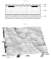
- FIG. 4 is a view showing an embodied example of FIG. 3C , also showing measurement results through a three-dimensional measurement device of a glass surface embodied by the method proposed in the first embodiment of the present invention.
- irregular etching of the ITO layer 200 forms a negative-type embossing having various widths of about 5 to 60 ⁇ m, heights of about 2 to 50 ⁇ m, and angles of about 2 to 30°.
- the haze has a value of about 10 to 50% to accomplish effects of the anti-glare film or functional polarizer.
- FIGS. 5A to 5C are cross-sectional views illustrating a method of fabricating a liquid crystal display device in accordance with a second exemplary embodiment of the present invention
- FIG. 6 is a view showing an embodied example of FIG. 5C .
- a transparent conductive layer through which light can readily pass for example, an indium tin oxide (ITO) layer is formed to a predetermined thickness on the upper substrate 110 exposed to the exterior of the liquid crystal to panel 100 using a general sputtering method. Then, the ITO layer is patterned using a general photolithography process to form a black matrix BM, i.e., an ITO pattern 200 ′ corresponding to the non-transmission region.
- ITO indium tin oxide
- a hydrofluoric (HF) acid-based etchant is used on the entire surface of the resultant structure, i.e., the liquid crystal panel 100 to etch the liquid crystal panel 100 for a certain time (preferably, about 1 to 5 minutes). At this time, the liquid crystal panel 100 is etched to have irregularities smaller than micron size due to structural characteristics of the ITO pattern 200 ′.
- HF hydrofluoric
- prominences and depressions R are initially formed on the upper substrate 110 in an embossed manner due to ITO, which is amorphous, having different etch rates.
- the ITO pattern 200 ′ is entirely etched, and the upper substrate 110 is also partially etched along with the ITO pattern 200 ′.
- the transmission region is etched to remove a portion of the upper substrate 110 without the prominences and depressions R, it is possible to prevent a decrease in transmissivity.
- the non-transmission region is etched to form prominences and depressions R in a micron size on the surface of the upper substrate 110 to make it possible to reduce specular reflection by external light and thereby improve readability, transmissivity, and contrast ratio (CR).
- the etching process using such a hydrofluoric acid-based etchant may be simultaneously performed on upper and lower parts of the liquid crystal panel 100 .
- the etching process using such a hydrofluoric acid-based etchant may be performed before performing a color filter process on the upper substrate 110 .
- an anti-reflective (AR) or low reflectance (LR) polarizer may be attached to the upper substrate 110 and additionally anti-reflective coating may be performed on the upper substrate 110 to constitute an anti-glare/anti-reflective (AR) polarizer.
- FIG. 6 is a view showing an embodied example of FIG. 5C , also showing measurement results through a three-dimensional measurement device of a glass surface embodied by the method proposed in the second embodiment of the present invention.
- the resultant embossing has a width of about 5 to 60 ⁇ m, and a height of about 2 to 10 ⁇ m.
- the transparent conductive layer and the substrate are simultaneously etched to form more irregular and fine prominences and depressions on the substrate, thereby preventing glare to obtain good readability and image clearness.
- reflection of the external light is excluded to accomplish a good contrast ratio.
- the method in accordance with the present invention can lower a reflection ratio to about 50% in comparison with the conventional method of directly etching the substrate to lower a surface reflection ratio.
- the method in accordance with the present invention can reduce cost and provide advantages in product competitiveness in comparison with the conventional method using a compensation film or a functional polarizer.
- both sides of the substrate are etched by performing surface treatment for readability, it is possible to reduce the thickness of the substrate and increase transmissivity.
- the method of fabricating a liquid crystal display device in accordance with an exemplary embodiment of the present invention may be applied to all liquid crystal display devices using optical anisotropy and polarization of liquid crystal, in addition to the conventional in-plan switching (IPS) or fringe field switching (FFS) mode liquid crystal display device.
- IPS in-plan switching
- FFS fringe field switching
- the transparent conductive layer and the substrate are simultaneously etched to form a more irregular surface on the substrate, thereby preventing glare to improve readability, image clarity, and contrast ratio.
Abstract
Description
Claims (9)
Applications Claiming Priority (2)
| Application Number | Priority Date | Filing Date | Title |
|---|---|---|---|
| KR10-2007-0035916 | 2007-04-12 | ||
| KR1020070035916A KR100843386B1 (en) | 2007-04-12 | 2007-04-12 | A method for fabricating liquid crystal display device |
Publications (2)
| Publication Number | Publication Date |
|---|---|
| US20080254559A1 US20080254559A1 (en) | 2008-10-16 |
| US7718329B2 true US7718329B2 (en) | 2010-05-18 |
Family
ID=39823587
Family Applications (1)
| Application Number | Title | Priority Date | Filing Date |
|---|---|---|---|
| US12/099,630 Active 2028-07-05 US7718329B2 (en) | 2007-04-12 | 2008-04-08 | Method of fabricating liquid crystal display device |
Country Status (5)
| Country | Link |
|---|---|
| US (1) | US7718329B2 (en) |
| JP (1) | JP5258359B2 (en) |
| KR (1) | KR100843386B1 (en) |
| CN (1) | CN101285956B (en) |
| TW (1) | TWI434118B (en) |
Cited By (1)
| Publication number | Priority date | Publication date | Assignee | Title |
|---|---|---|---|---|
| US20160124262A1 (en) * | 2014-10-30 | 2016-05-05 | Boe Technology Group Co., Ltd. | Display panel, display device and manufacturing method thereof |
Families Citing this family (2)
| Publication number | Priority date | Publication date | Assignee | Title |
|---|---|---|---|---|
| JP2012094630A (en) * | 2010-10-26 | 2012-05-17 | Toshiba Corp | Semiconductor light-emitting element |
| US10802325B2 (en) * | 2018-11-05 | 2020-10-13 | Himax Display, Inc. | Display panel |
Citations (9)
| Publication number | Priority date | Publication date | Assignee | Title |
|---|---|---|---|---|
| KR20010003045A (en) | 1999-06-21 | 2001-01-15 | 김영환 | Method for manufacturing organic field emission display device |
| US6879361B2 (en) * | 2001-08-01 | 2005-04-12 | Samsung Electronics Co., Ltd. | Transreflective liquid crystal display and method of manufacturing the same |
| US6946679B2 (en) * | 2000-01-13 | 2005-09-20 | Seiko Epson Corporation | Liquid crystal display device, manufacturing method therefor, and electronic apparatus |
| KR20050110541A (en) | 2004-05-19 | 2005-11-23 | 삼성에스디아이 주식회사 | Method for fabrication of organic electro luminescence device |
| US20070013648A1 (en) * | 2005-07-14 | 2007-01-18 | Alps Electric Co., Ltd. | Display element, method of producing display element, and electronic apparatus including display element |
| US7215399B2 (en) * | 2002-12-31 | 2007-05-08 | Lg.Philips Lcd Co. Ltd | Method of manufacturing array substrate for liquid crystal display device |
| US20070151596A1 (en) * | 2004-02-20 | 2007-07-05 | Sharp Kabushiki Kaisha | Substrate for photoelectric conversion device, photoelectric conversion device, and stacked photoelectric conversion device |
| US7348222B2 (en) * | 2003-06-30 | 2008-03-25 | Semiconductor Energy Laboratory Co., Ltd. | Method for manufacturing a thin film transistor and method for manufacturing a semiconductor device |
| US7364808B2 (en) * | 2001-10-19 | 2008-04-29 | Asahi Glass Company, Limited | Substrate with transparent conductive oxide film, process for its production and photoelectric conversion element |
Family Cites Families (6)
| Publication number | Priority date | Publication date | Assignee | Title |
|---|---|---|---|---|
| JPS63228535A (en) * | 1987-03-18 | 1988-09-22 | 沖電気工業株式会社 | Formation of electrode pattern |
| JP2610698B2 (en) * | 1990-07-17 | 1997-05-14 | シャープ株式会社 | Method for manufacturing reflective liquid crystal display device |
| JP3531995B2 (en) * | 1995-03-27 | 2004-05-31 | 株式会社東芝 | Manufacturing method of liquid crystal display device |
| JPH11264967A (en) * | 1998-03-17 | 1999-09-28 | Toshiba Corp | Liquid crystal display |
| JP2000231007A (en) * | 1999-02-09 | 2000-08-22 | Ricoh Opt Ind Co Ltd | Formation of array pattern with fine recesses and planar lens array, liquid crystal display device and planar oil trap produced by the forming method |
| JP4207599B2 (en) * | 2003-02-24 | 2009-01-14 | ソニー株式会社 | Manufacturing method of liquid crystal panel |
-
2007
- 2007-04-12 KR KR1020070035916A patent/KR100843386B1/en active IP Right Grant
-
2008
- 2008-04-03 TW TW097112345A patent/TWI434118B/en active
- 2008-04-08 JP JP2008100595A patent/JP5258359B2/en active Active
- 2008-04-08 US US12/099,630 patent/US7718329B2/en active Active
- 2008-04-09 CN CN2008100906909A patent/CN101285956B/en active Active
Patent Citations (9)
| Publication number | Priority date | Publication date | Assignee | Title |
|---|---|---|---|---|
| KR20010003045A (en) | 1999-06-21 | 2001-01-15 | 김영환 | Method for manufacturing organic field emission display device |
| US6946679B2 (en) * | 2000-01-13 | 2005-09-20 | Seiko Epson Corporation | Liquid crystal display device, manufacturing method therefor, and electronic apparatus |
| US6879361B2 (en) * | 2001-08-01 | 2005-04-12 | Samsung Electronics Co., Ltd. | Transreflective liquid crystal display and method of manufacturing the same |
| US7364808B2 (en) * | 2001-10-19 | 2008-04-29 | Asahi Glass Company, Limited | Substrate with transparent conductive oxide film, process for its production and photoelectric conversion element |
| US7215399B2 (en) * | 2002-12-31 | 2007-05-08 | Lg.Philips Lcd Co. Ltd | Method of manufacturing array substrate for liquid crystal display device |
| US7348222B2 (en) * | 2003-06-30 | 2008-03-25 | Semiconductor Energy Laboratory Co., Ltd. | Method for manufacturing a thin film transistor and method for manufacturing a semiconductor device |
| US20070151596A1 (en) * | 2004-02-20 | 2007-07-05 | Sharp Kabushiki Kaisha | Substrate for photoelectric conversion device, photoelectric conversion device, and stacked photoelectric conversion device |
| KR20050110541A (en) | 2004-05-19 | 2005-11-23 | 삼성에스디아이 주식회사 | Method for fabrication of organic electro luminescence device |
| US20070013648A1 (en) * | 2005-07-14 | 2007-01-18 | Alps Electric Co., Ltd. | Display element, method of producing display element, and electronic apparatus including display element |
Cited By (2)
| Publication number | Priority date | Publication date | Assignee | Title |
|---|---|---|---|---|
| US20160124262A1 (en) * | 2014-10-30 | 2016-05-05 | Boe Technology Group Co., Ltd. | Display panel, display device and manufacturing method thereof |
| US9927648B2 (en) * | 2014-10-30 | 2018-03-27 | Boe Technology Group Co., Ltd. | Manufacturing methods of display panel and display device |
Also Published As
| Publication number | Publication date |
|---|---|
| CN101285956B (en) | 2012-06-13 |
| KR100843386B1 (en) | 2008-07-03 |
| TWI434118B (en) | 2014-04-11 |
| JP5258359B2 (en) | 2013-08-07 |
| US20080254559A1 (en) | 2008-10-16 |
| JP2008262202A (en) | 2008-10-30 |
| TW200844619A (en) | 2008-11-16 |
| CN101285956A (en) | 2008-10-15 |
Similar Documents
| Publication | Publication Date | Title |
|---|---|---|
| TWI432796B (en) | Color filter substrate for liquid crystal display and method of fabricating the same | |
| KR100734461B1 (en) | Liquid crystal display device | |
| US9195110B2 (en) | Liquid crystal display device and process for producing the same | |
| JP2009271390A (en) | Liquid crystal display and electronic equipment | |
| JP2793076B2 (en) | Reflective liquid crystal display device and method of manufacturing the same | |
| JP2000009911A (en) | Diffusion reflection plate, its production and reflection display device | |
| WO2019047461A1 (en) | Liquid crystal panel and fabrication method therefor | |
| KR100864551B1 (en) | Liquid crystal display device | |
| US10942390B2 (en) | Display substrate and fabricating method thereof, and display panel | |
| KR20070105092A (en) | Array substrate and display panel having the same | |
| US7718329B2 (en) | Method of fabricating liquid crystal display device | |
| JP2004151459A (en) | Substrate for liquid crystal display and liquid crystal display equipped with the same | |
| CN106990597B (en) | Color filter substrate, manufacturing method thereof, display panel and display device | |
| US20070085956A1 (en) | Multi-domain vertical alignment thin film transistor liquid crystal display, color filter substrate and polarizer film applied thereto, and fabricating method thereof | |
| TW574566B (en) | Liquid crystal display element | |
| JP2000010124A (en) | Reflection type liquid crystal display device and its production | |
| JPH05281533A (en) | Reflection type liquid crystal display device and its manufacture | |
| JP4187194B2 (en) | Liquid crystal display element | |
| JP2005141145A (en) | Liquid crystal display and manufacturing method of color filter substrate | |
| KR20020053575A (en) | Liquid crystal display device and method for manufacturing the same | |
| TWI400490B (en) | Color filter substrate structure of liquid crystal display and method for manufacturing the same | |
| KR20040037943A (en) | Device and fabrication method for polarizer in substrate of lcd | |
| US20080299328A1 (en) | Liquid crystal display fabrication and device | |
| JP2001166286A (en) | Method of manufacturing light reflecting substrate and liquid crystal display element | |
| KR101993884B1 (en) | Liquid crystal display device and method for fabricating the same |
Legal Events
| Date | Code | Title | Description |
|---|---|---|---|
| AS | Assignment |
Owner name: BOE HYDIS TECHNOLOGY CO., LTD., KOREA, DEMOCRATIC Free format text: ASSIGNMENT OF ASSIGNORS INTEREST;ASSIGNORS:CHOI, SUK;JANG, SOON JU;KIM, BYUNG HOON;REEL/FRAME:020772/0707 Effective date: 20080318 Owner name: BOE HYDIS TECHNOLOGY CO., LTD.,KOREA, DEMOCRATIC P Free format text: ASSIGNMENT OF ASSIGNORS INTEREST;ASSIGNORS:CHOI, SUK;JANG, SOON JU;KIM, BYUNG HOON;REEL/FRAME:020772/0707 Effective date: 20080318 |
|
| FEPP | Fee payment procedure |
Free format text: PAYOR NUMBER ASSIGNED (ORIGINAL EVENT CODE: ASPN); ENTITY STATUS OF PATENT OWNER: LARGE ENTITY |
|
| AS | Assignment |
Owner name: HYDIS TECHNOLOGIES CO., LTD.,KOREA, REPUBLIC OF Free format text: CHANGE OF NAME;ASSIGNOR:BOE HYDIS TECHNOLOGY CO., LTD.;REEL/FRAME:024013/0075 Effective date: 20080130 |
|
| STCF | Information on status: patent grant |
Free format text: PATENTED CASE |
|
| FPAY | Fee payment |
Year of fee payment: 4 |
|
| FEPP | Fee payment procedure |
Free format text: PAT HOLDER CLAIMS SMALL ENTITY STATUS, ENTITY STATUS SET TO SMALL (ORIGINAL EVENT CODE: LTOS); ENTITY STATUS OF PATENT OWNER: LARGE ENTITY |
|
| MAFP | Maintenance fee payment |
Free format text: PAYMENT OF MAINTENANCE FEE, 8TH YR, SMALL ENTITY (ORIGINAL EVENT CODE: M2552) Year of fee payment: 8 |
|
| FEPP | Fee payment procedure |
Free format text: ENTITY STATUS SET TO UNDISCOUNTED (ORIGINAL EVENT CODE: BIG.); ENTITY STATUS OF PATENT OWNER: LARGE ENTITY |
|
| MAFP | Maintenance fee payment |
Free format text: PAYMENT OF MAINTENANCE FEE, 12TH YEAR, LARGE ENTITY (ORIGINAL EVENT CODE: M1553); ENTITY STATUS OF PATENT OWNER: LARGE ENTITY Year of fee payment: 12 |
|
| MAFP | Maintenance fee payment |
Free format text: PAYMENT OF MAINTENANCE FEE UNDER 1.28(C) (ORIGINAL EVENT CODE: M1559); ENTITY STATUS OF PATENT OWNER: LARGE ENTITY |