US7724589B2 - System and method for delaying a signal communicated from a system to at least one of a plurality of memory circuits - Google Patents
System and method for delaying a signal communicated from a system to at least one of a plurality of memory circuits Download PDFInfo
- Publication number
- US7724589B2 US7724589B2 US11/461,430 US46143006A US7724589B2 US 7724589 B2 US7724589 B2 US 7724589B2 US 46143006 A US46143006 A US 46143006A US 7724589 B2 US7724589 B2 US 7724589B2
- Authority
- US
- United States
- Prior art keywords
- signal
- circuits
- memory
- delay
- sub
- Prior art date
- Legal status (The legal status is an assumption and is not a legal conclusion. Google has not performed a legal analysis and makes no representation as to the accuracy of the status listed.)
- Active
Links
Images


Classifications
-
- G—PHYSICS
- G11—INFORMATION STORAGE
- G11C—STATIC STORES
- G11C8/00—Arrangements for selecting an address in a digital store
- G11C8/18—Address timing or clocking circuits; Address control signal generation or management, e.g. for row address strobe [RAS] or column address strobe [CAS] signals
-
- G—PHYSICS
- G11—INFORMATION STORAGE
- G11C—STATIC STORES
- G11C11/00—Digital stores characterised by the use of particular electric or magnetic storage elements; Storage elements therefor
- G11C11/21—Digital stores characterised by the use of particular electric or magnetic storage elements; Storage elements therefor using electric elements
- G11C11/34—Digital stores characterised by the use of particular electric or magnetic storage elements; Storage elements therefor using electric elements using semiconductor devices
- G11C11/40—Digital stores characterised by the use of particular electric or magnetic storage elements; Storage elements therefor using electric elements using semiconductor devices using transistors
- G11C11/401—Digital stores characterised by the use of particular electric or magnetic storage elements; Storage elements therefor using electric elements using semiconductor devices using transistors forming cells needing refreshing or charge regeneration, i.e. dynamic cells
- G11C11/406—Management or control of the refreshing or charge-regeneration cycles
- G11C11/40618—Refresh operations over multiple banks or interleaving
-
- G—PHYSICS
- G11—INFORMATION STORAGE
- G11C—STATIC STORES
- G11C29/00—Checking stores for correct operation ; Subsequent repair; Testing stores during standby or offline operation
- G11C29/04—Detection or location of defective memory elements, e.g. cell constructio details, timing of test signals
- G11C29/50—Marginal testing, e.g. race, voltage or current testing
- G11C29/50012—Marginal testing, e.g. race, voltage or current testing of timing
-
- G—PHYSICS
- G11—INFORMATION STORAGE
- G11C—STATIC STORES
- G11C5/00—Details of stores covered by group G11C11/00
- G11C5/02—Disposition of storage elements, e.g. in the form of a matrix array
- G11C5/04—Supports for storage elements, e.g. memory modules; Mounting or fixing of storage elements on such supports
-
- G—PHYSICS
- G11—INFORMATION STORAGE
- G11C—STATIC STORES
- G11C7/00—Arrangements for writing information into, or reading information out from, a digital store
- G11C7/10—Input/output [I/O] data interface arrangements, e.g. I/O data control circuits, I/O data buffers
- G11C7/1051—Data output circuits, e.g. read-out amplifiers, data output buffers, data output registers, data output level conversion circuits
- G11C7/1066—Output synchronization
-
- G—PHYSICS
- G11—INFORMATION STORAGE
- G11C—STATIC STORES
- G11C8/00—Arrangements for selecting an address in a digital store
- G11C8/12—Group selection circuits, e.g. for memory block selection, chip selection, array selection
-
- G—PHYSICS
- G11—INFORMATION STORAGE
- G11C—STATIC STORES
- G11C11/00—Digital stores characterised by the use of particular electric or magnetic storage elements; Storage elements therefor
- G11C11/21—Digital stores characterised by the use of particular electric or magnetic storage elements; Storage elements therefor using electric elements
- G11C11/34—Digital stores characterised by the use of particular electric or magnetic storage elements; Storage elements therefor using electric elements using semiconductor devices
- G11C11/40—Digital stores characterised by the use of particular electric or magnetic storage elements; Storage elements therefor using electric elements using semiconductor devices using transistors
- G11C11/401—Digital stores characterised by the use of particular electric or magnetic storage elements; Storage elements therefor using electric elements using semiconductor devices using transistors forming cells needing refreshing or charge regeneration, i.e. dynamic cells
- G11C11/406—Management or control of the refreshing or charge-regeneration cycles
Definitions
- the present invention relates to memory, and more particularly to multiple-memory circuit systems.
- a system and method are provided for delaying a signal communicated from a system to a plurality of memory circuits. Included is a component in communication with a plurality of memory circuits and a system. Such component is operable to receive a signal from the system and communicate the signal to at least one of the memory circuits after a delay. In other embodiments, the component is operable to receive a signal from at least one of the memory circuits and communicate the signal to the system after a delay.
- FIG. 1 illustrates a multiple memory circuit framework, in accordance with one embodiment.
- FIGS. 2A-2E show various configurations of a buffered stack of dynamic random access memory (DRAM) circuits with a buffer chips in accordance with various embodiments.
- DRAM dynamic random access memory
- FIG. 2F illustrates a method for storing at least a portion of information received in association with a first operation for use in performing a second operation, in accordance with still another embodiment.
- FIG. 3 shows a high capacity dual in-line memory module (DIMM) using buffered stacks, in accordance with still yet another embodiment.
- DIMM dual in-line memory module
- FIG. 4 shows a timing design of a buffer chip that makes a buffered stack of DRAM circuits mimic longer column address strobe (CAS) latency DRAM to a memory controller, in accordance with another embodiment.
- CAS column address strobe
- FIG. 5 shows the write data timing expected by DRAM in a buffered stack, in accordance with vet another embodiment.
- FIG. 6 shows write control signals delayed by a buffer chips, in accordance with still yet another embodiment.
- FIG. 7 shows early write data from an advanced memory buffer (AMB), in accordance with another embodiment.
- AMB advanced memory buffer
- FIG. 8 shows address bus conflicts caused by delayed write operations, in accordance with yet another embodiment.
- FIGS. 9A-B show variable delays of operations through a buffer chip, in accordance with another embodiment.
- FIG. 10 shows a buffered stack of four 512 Mb DRAM circuits mapped to a single 2 Gb DRAM circuit, in accordance with yet another embodiment.
- FIG. 11 illustrates a method for refreshing a plurality of memory circuits, in accordance with still yet another embodiment.
- FIG. 1 illustrates a multiple memory circuit framework 100 , in accordance with one embodiment. As shown, included are an interface circuit 102 , a plurality of memory circuits 104 A, 104 B, 104 N, and a system 106 . In the context of the present description, such memory circuits 104 A, 104 B, 104 N may include any circuit capable of serving as memory.
- one or more of the memory circuits 104 A, 104 B, 104 N may include a monolithic memory circuit.
- such monolithic memory circuit may take the form of dynamic random access memory (DRAM).
- DRAM may take any form including, but not limited to synchronous (SDRAM), double data rate synchronous (DDR DRAM, DDR2 DRAM, DDR3 DRAM, etc.), quad data rate (QDR DRAM), direct RAMBUS (DRDRAM), fast page mode (FPM DRAM), video (VDRAM), extended data out (EDO DRAM), burst EDO (BEDO DRAM), multibank (MDRAM), synchronous graphics (SGRAM), and/or any other type of DRAM.
- SDRAM synchronous
- DDR DRAM double data rate synchronous
- DDR2 DRAM double data rate synchronous
- DDR3 DRAM etc.
- quad data rate quad data rate
- DRAM direct RAMBUS
- FPM DRAM fast page mode
- VDRAM video
- EDO DRAM extended data out
- one or more of the memory circuits 104 A, 104 B, 104 N may include other types of memory such as magnetic random access memory (MRAM), intelligent random access memory (IRAM), distributed network architecture (DNA) memory, window random access memory (WRAM), flash memory (e.g. NAND, NOR, or others, etc.), pseudostatic random access memory (PSRAM), wetware memory, and/for any other type of memory circuit that meets the above definition.
- MRAM magnetic random access memory
- IRAM intelligent random access memory
- DNA distributed network architecture
- WRAM window random access memory
- flash memory e.g. NAND, NOR, or others, etc.
- PSRAM pseudostatic random access memory
- wetware memory wetware memory
- the memory circuits 104 A, 104 B, 104 N may be symmetrical or asymmetrical.
- the memory, circuits 104 A, 104 B, 104 N may be of the same type, brand, and/or size, etc.
- one or more of the memory circuits 104 A, 104 B, 104 N may be of a first type, brand, and/or size; while one or more other memory circuits 104 A, 104 B, 104 N may be of a second type, brand, and/or size, etc.
- one or more memory circuits 104 A, 104 B, 104 N may be of a DRAM type, while one or more other memory circuits 104 A, 104 B, 104 N may be of a flash type. While three or more memory circuits 104 A, 104 B, 104 N are shown in FIG. 1 in accordance with one embodiment, it should be noted that any plurality of memory circuits 104 A, 104 B, 104 N may be employed.
- the memory circuits 104 A, 104 B, 104 N may or may not be positioned on at least one dual in-line memory module (DIMM) (not shown).
- the DIMM may include a registered DIMM (R-DIMM), a small outline-DIMM (SO-DIMM), a fully buffered-DIMM (FB-DIMM), an un-buffered DIMM, etc.
- R-DIMM registered DIMM
- SO-DIMM small outline-DIMM
- FB-DIMM fully buffered-DIMM
- the memory circuits 104 A, 104 B, 104 N may or may not be positioned on any desired entity, for packaging purposes.
- the system 106 include any system capable of requesting and/or initiating a process that results in an access of the memory circuits 104 A, 104 B, 104 N. As an option, the system 106 may accomplish this utilizing a memory controller (not shown), or any other desired mechanism.
- a memory controller not shown
- such system 106 may include a host system in the form of a desktop computer, lap-top computer, server, workstation, a personal digital assistant (PDA) device, a mobile phone device, a television, a peripheral device (e.g. printer, etc.).
- PDA personal digital assistant
- a mobile phone device e.g. printer, etc.
- a peripheral device e.g. printer, etc.
- such interface circuit 102 may include any, circuit capable of indirectly or directly communicating with the memory circuits 104 A, 104 B, 104 N and the system 106 .
- the interface circuit 102 may include one or more interface circuits, a buffer chip, etc. Embodiments involving, such a buffer chip will be set forth hereinafter during reference to subsequent figures.
- the interface circuit 102 may or may not be manufactured in monolithic form.
- any of such pans (or portions thereof) may or may not be integrated in any desired manner.
- such optional integration may involve simply packaging such parts together (e.g. stacking the parts, etc.) and/or integrating them monolithically.
- one or more portions (or all, for that matter) of the interface circuit 102 may or may not be packaged with one or more of the memory circuits 104 , 104 B, 104 N (or all, for that matter).
- Different optional embodiments which may be implemented in accordance with the present multiple memory circuit framework 100 will be set forth hereinafter during reference to FIGS. 2A-2E , and 3 et al.
- the interlace circuit 102 may be capable of various functionality, in the context of different embodiments. More illustrative information will now be set forth regarding such optional functionally which may or may not be implemented in the context of such interface circuit 102 , per the desires of the user. It should be strongly noted that the following information is set forth for illustrative purposes and should not be construed as limiting in any manner. For example, any of the following features may be optionally incorporated with or without the exclusion of other features described.
- the interface circuit 102 interfaces a plurality, of signals 108 that are communicated between the memory, circuits 104 A, 104 B, 104 N and the system 106 .
- signals may, for example, include address/control/clock signals, etc.
- the interfaced signals 108 may represent all of the signals that are communicated between the memory circuits 104 A, 104 B, 104 N and the system 106 .
- at least a portion of signals 110 may travel directly between the memory circuits 104 A, 104 B, 104 N and the system 106 or component thereof [e.g.
- the number of the signals 108 may vary such that the signals 108 are a majority or more (L>M), etc.
- the interlace circuit 102 may be (operable to interface a first number of memory circuits 104 A, 104 B, 104 N and the system 106 for simulating at least one memory circuit of a second number.
- the simulation may refer to any simulating, emulating, disguising, transforming, converting, and/or the like that results in at least one aspect (e.g. a number in this embodiment, etc.) of the memory circuits 104 A, 104 B, 104 N appearing different to the system 106 .
- the simulation may be electrical in nature, logical in nature, protocol in nature, and/or performed in any other desired manner.
- a number of pins, wires, signals, etc. may be simulated, while, in the context of logical simulation, a particular function may be simulated.
- a particular protocol e.g. DDR3, etc.
- DDR3 DDR3, etc.
- the second number may be more or less than the first number. Still yet, in the latter case, the second number may be one, such that a single memory circuit is simulated.
- Different optional embodiments which may employ various aspects of the present embodiment will be set forth hereinafter during, reference to FIGS. 2A-2E , and 3 et al.
- the interface circuit 102 may be operable to interface the memory circuits 104 A, 104 B, 104 N and the system 106 for simulating at least one memory circuit with at least one aspect that is different from at least one aspect of at least one of the plurality of the memory circuits 104 A, 104 B, 104 N.
- such aspect may include a signal, a capacity, a timing, a logical interface, etc.
- any aspect associated with one or more of the memory circuits 104 A, 104 B, 104 N may be simulated differently in the foregoing manner.
- such signal may refer to a control signal (e.g. an address signal; a signal associated with an activate operation precharge operation write operation, read operation, a mode register write operation, a mode register read operation, a refresh operation; etc.), a data signal, a logical or physical signal, or any other signal for that matter.
- a control signal e.g. an address signal; a signal associated with an activate operation precharge operation write operation, read operation, a mode register write operation, a mode register read operation, a refresh operation; etc.
- a data signal e.g. an address signal; a signal associated with an activate operation precharge operation write operation, read operation, a mode register write operation, a mode register read operation, a refresh operation; etc.
- protocol such may, in one exemplary embodiment, refer to a particular standard protocol.
- a number of memory circuits 104 A, 104 B, 104 N that obey a standard protocol may be used to simulate one or more memory circuits that obey a different protocol (e.g. DDR3, etc.).
- a number of memory circuits 104 A, 104 B, 104 N, that obey a version of protocol e.g. DDR2 with 3-3-3 latency timing, etc.
- DDR2 with 3-3-3 latency timing, etc.
- a different version of the same protocol e.g. DDR2 with 5-5-5 latency timing, etc.
- the interface circuit 102 may be operable for simulating at least one memory circuit with a first memory capacity that is greater than (or less than) a second memory capacity, of at least one of the memory circuits 104 A, 104 B, 104 N.
- timing may possibly relate to a latency (e.g. time delay, etc.).
- a latency e.g. time delay, etc.
- such latency may include a column address strobe (CAS) latency, which refers to a latency associated with accessing a column of data.
- the latency may include a row address to column address latency (tRCD), which refers to a latency required between the row address strobe (RAS) and CAS.
- tRP row precharge latency
- tRP row precharge latency
- the latency may include an activate to precharge latency (tRAS), which refers to a latency required to access a certain row of data between an activate operation and a precharge operation.
- tRAS activate to precharge latency
- the interface circuit 102 may be operable for simulating at least one memory circuit with a first latency that is longer (or shorter) than a second latency of at least one of the memory circuits 104 A, 104 B, 104 N.
- tRAS activate to precharge latency
- a component may be operable to receive a signal from the system 106 and communicate the signal to at least one of the memory circuits 104 A, 104 B, 104 N after a delay.
- the signal may refer to a control signal (e.g. an address signal; a signal associated with an activate operation, precharge operation, write operation, read operation; etc.), a data signal, a logical or physical signal, or any other signal for that matter.
- such delay may be fixed or variable (e.g. a function of the current signal, the previous signal, etc.).
- the component may be operable to receive a signal from at least one of the memory circuits 104 A, 104 B, 104 N and communicate the sisal to the system 106 after a delay.
- the delay may include a cumulative delay associated with any one or more of the aforementioned signals. Even still, the delay may result in a time shift of the signal forward and/or back in time (with respect to other signals). Of course, such forward and backward time shift may or may not be equal in magnitude. In one embodiment, this time shifting may be accomplished by utilizing a plurality of delay functions which each apply a different delay to a different signal. In still additional embodiments, the aforementioned shifting may be coordinated among multiple signals such that different signals are subject to shifts with different relative directions/magnitudes, in an organized fashion.
- the aforementioned component may, but need not necessarily take the form of the interface circuit 102 of FIG. 1 .
- the component may include a register, an AMB, a component positioned on at least one DIMM, a memory controller, etc.
- Such register may, in various embodiments, include a Joint Electron Device Engineering Council (JEDEC) register, a JEDEC register including one or more functions set forth herein, a register with forwarding, storing and/or buffering capabilities, etc.
- JEDEC Joint Electron Device Engineering Council
- At least one of a plurality of memory circuits 104 A, 104 B, 104 N may be identified that is not currently being accessed by the system 106 .
- identification may involve determining whether a page [i.e. any portion of any memory(s), etc.] is being accessed in at least one of the plurality of memory circuits 104 A, 104 B, 104 N.
- any other technique may be used that results in the identification of at least one of the memory circuits 104 A, 104 B, 104 N that is not being accessed.
- a power saving operation is initiated in association with the at least one memory circuits 104 A, 104 B, 104 N.
- such power saving operation may involve a power down operation and, in particular, a precharge power down operation.
- a power down operation may involve a power down operation and, in particular, a precharge power down operation.
- a precharge power down operation may be employed in the context of the present embodiment.
- the present functionality or a portion thereof may be carried out utilizing any desired component.
- such component may, but need not necessarily take the form of the interface circuit 102 of FIG. 1 .
- the component may include a register, an AMB, a component positioned on at least one DIMM, a memory controller, etc.
- One optional embodiment which employs various features of the present embodiment will be set forth hereinafter during reference to FIG. 10 .
- a plurality of the aforementioned components may serve, in combination to interface the memory circuits 104 A, 104 B, 104 N and the system 106 .
- two, three, four, or more components many accomplish this.
- the different components may be relatively configured in any desired manner.
- the components may be configured in parallel, serially, or a combination thereof.
- any number of the components may be allocated to any number of the memory, circuits 104 A, 104 B, 104 N.
- each of the plurality of components may be the same or different. Still yet, the components may share the same or similar interface tasks and/or perform different interface tasks. Such interface tasks may include, but are not limited to simulating one or more aspects of a memory circuit, performing a power savings/refresh operation, carrying out any one or more of the various functionalities set forth herein, and/or any other task relevant to the aforementioned interfacing.
- interface tasks may include, but are not limited to simulating one or more aspects of a memory circuit, performing a power savings/refresh operation, carrying out any one or more of the various functionalities set forth herein, and/or any other task relevant to the aforementioned interfacing.
- One optional embodiment which employs various features of the present embodiment will be set forth hereinafter during reference to FIG. 3 .
- an embodiment is set forth for storing at least a portion of information received in association with a first operation for use in performing a second operation. See FIG. 2F .
- a technique is provided for refreshing, a plurality of memory circuits, in accordance with still vet another embodiment. See FIG. 11 .
- FIGS. 2A-2E show various configurations of a buffered stack of DRAM circuits 206 A-D with a buffer chip 202 , in accordance with various embodiments.
- the various configurations to be described in the following embodiments may be implemented in the context of the architecture and/or environment of FIG. 1 . Of course, however, they may also be carried out in any other desired environment (e.g. using other memory types, etc.). It should also be noted that the aforementioned definitions may apply during the present description.
- the buffer chip 202 is placed electrically between an electronic host system 204 and a stack of DRAM circuits 206 A-D.
- a stack may refer to any collection of memory circuits.
- the buffer chip 202 may include any device capable of buffering a stack of circuits (e.g. DRAM circuits 206 A-D, etc.).
- the buffer chip 202 may be capable of buffering the stack of DRAM circuits 206 A-D to electrically and/or logically resemble at least one larger capacity DRAM circuit to the host system 204 . In this way the stack of DRAM circuits 206 A-D may appear as a smaller quantity of larger capacity DRAM circuits to the host system 204 .
- the stack of DRAM circuits 206 A-D may include eight 512 Mb DRAM circuits.
- the buffer chip 202 may buffer the stack of eight 512 Mb DRAM circuits to resemble a single 4 Gb DRAM circuit to a memory controller (not shown) of the associated host system 204 .
- the buffer chip 202 may buffer the stack of eight 512 Mb DRAM circuits to resemble two 2 Gb DRAM circuits to a memory controller of an associated host system 204 .
- the stack of DRAM circuits 206 A-D may include any number of DRAM circuits. Just by way of example a bunter chip 202 may be connected to 2, 4, 8 or more DRAM circuits 206 A-D. Also, the DRAM circuits 206 A-D may be arranged in a single stack, as shown in FIGS. 2A-2D .
- the DRAM circuits 206 A-D may be arranged on a single side of the buffer chip 202 , as shown in FIGS. 2A-2D . Of course, however, the DRAM circuits 206 A-D may be located on both sides of the buffer chip 202 shown in FIG. 2 . Thus, for example, a buffer chip 202 may be connected to 16 DRAM circuits with 8 DRAM circuits on either side of the buffer chip 202 , where the 8 DRAM circuits on each side of the buffer chip 202 are arranged in two stacks of four DRAM circuits.
- the buffer chip 202 may optionally be a part of the stack of DRAM circuits 206 A-D. Of course, however, the buffer chip 202 may also be separate from the stack of DRAM circuits 206 A-D. In addition, the buffer chip 202 may be physically located anywhere in the stack of DRAM circuits 206 A-D, where such buffer chip 202 electrically sits between the electronic host system 204 and the stack of DRAM circuits 206 A-D.
- a memory bus (not shown) may connect to the buffer chip 202 , and the buffer chip 202 may connect to each of the DRAM circuits 206 A-D in the stack.
- the buffer chip 202 may be located at the bottom of the stack of DRAM circuits 206 A-D (e.g. the bottom-most device in the stack).
- the buffer chip 202 may be located in the middle of the stack of DRAM circuits 206 A-D.
- the buffer chip 202 may be located at the top of the stack of DRAM circuits 206 A-D (e.g. the top-most device in the stack).
- the buffer chip 202 may be located anywhere between the two extremities of the stack of DRAM circuits 206 A-D.
- the electrical connections between the buffer chip 202 and the stack of DRAM circuits 206 A-D may be configured in any desired manner.
- address, control (e.g. command, etc.), and clock signals may be common to all DRAM circuits 206 A-D in the stack (e.g. using one common bus).
- data signals bay be wired as one common bus, several busses or as an individuals bus to each DRAM circuit 206 A-D.
- any combinations of such configurations may also be utilized.
- the stack of DRAM circuits 206 A-D may have one common address, control and clock bus 208 with individual data busses 210 .
- the stack of DRAM circuits 206 A-D may have two address, control and clock busses 208 along with two data busses 210 .
- the stack of DRAM circuits 206 A-D may have one address, control and clock bus 208 together with two data busses 210 .
- the stack of DRAM circuits 206 A-D may have one common address, control and clock bus 208 and one common data bus 210 . It should be noted that any other permutations and combinations of such address, control, clock and data buses may be utilized.
- FIG. 2F illustrates a method 280 for storing at least a portion of information received in association with a first operation for use in performing a second operation, in accordance with still yet an other embodiment.
- the method 280 may be implemented in the context of the architecture and/or environment of any one or more of FIGS. 1-2E .
- the method 280 may be carried out by the interface circuit 102 of FIG. 1 .
- the method 280 may be carried out in any desired environment. It should also be noted that the aforementioned definitions may apply during the present description.
- first information is received in association with a first operation to be performed on at least one of a plurality of memory circuits (e.g. see the memory circuits 104 A, 104 B, 104 N of FIG. 1 , etc.).
- first information may or may not be received coincidently with the first operation, as long as it is associated in some capacity.
- the first operation may, in one embodiment, include a row operation.
- the first information may include address information (e.g. a set of address bits, etc.).
- second information is received in association with a second operation. Similar to the first information, the second information may or may not be received coincidently with the second operation and may include address information. Such second operation, however, may, in one embodiment, include a column operation.
- the second operation may be performed utilizing the stored portion of the first information in addition to the second information. See operation 288 . More illustrative information will now be set forth regarding various optional features with which the foregoing method 280 may or may not be implemented, per the desires of the user. Specifically, an example will be set for illustrating the manner in which the method 280 may be employed for accommodating a buffer chip that is simulating at least one aspect of a plurality of memory circuits.
- the present example of the method 280 of FIG. 2F will be set forth in the context of the various components (e.g. buffer chip 202 , etc.) shown in the embodiments of FIGS. 2A-2E .
- the buffer chip 202 may receive more address bits from the memory controller than are required by the DRAM circuits 206 A-D in the stack. These extra address bits may be decoded by the buffer chip 202 to individually select the DRAM circuits 206 A-D in the stack, utilizing separate chip select signals to each of the DRAM circuits 206 A-D in the stack.
- a stack of four ⁇ 4 1 Gb DRAM circuits 206 A-D behind a buffer chip 202 may appear as a single ⁇ 4 4 Gb DRAM circuit to the memory controller.
- the memory controller for may provide sixteen row address bits and three bank address hits during a row (e.g. activate) operation, and provide eleven column address bits and three bank address bits during a column (e.g. read or write) operation.
- the individual DRAM circuits 206 A-D in the stack may require only fourteen row address bits and three bank address bits for a row operation, and eleven column address bits and three bank address bits during a column operation.
- the buffer chip 202 may receive two address bits more than are needed by each DRAM circuit 206 A-D in the stack.
- the buffer chip 202 may therefore use the two extra address bits from the memory controller to select one of the four DRAM circuits 206 A-D in the stack.
- the buffer chip 202 may receive the same number of address bits from the memory controller during a column operation as are needed by each DRAM circuit 206 A-D) in the stack.
- the buffer chip 202 may be designed to store the to extra address bits provided during a row operation and use the two stored address bits to select the correct DRAM circuit 206 A-D during the column operation.
- the mapping between a system address e.g. address from the memory controller, including the chip select signal(s) and a device address (e.g. the address, including the chip select signals, presented to the DRAMA circuits 206 A-D in the stack) may be performed by the buffer chip 202 in various manners.
- a lower order system row address and bank address bits may be mapped directly to tire device row address and bank address inputs.
- the most significant row address bit(s) and, optionally, the most significant bank address bit(s) may be decoded to generate the chip select signals for the DRAM circuits 206 A-D in the stack during a row operation.
- the address bits used to generate the chip select signals during the row operation may also be stored in an internal lookup table by the buffer chip 202 for one or more clock cycles.
- the system column address and bank address bits may be mapped directly to the device column address and bank address inputs, while the stored address bits may be decoded to generate the chip select signals.
- addresses may be mapped between four 512 Mb DRAM circuits 206 A-D that simulate a single 2 Gb DRAM circuits utilizing the buffer chip 202 .
- There may be 15 row address bits from the system 204 , such that row address bits 0 through 13 are mapped directly to the DRAM circuits 206 A-D.
- There may also be 3 bank address bits from the system 204 , such that bank address bits 0 through 1 are mapped directly to the DRAM circuits 206 A-D.
- the bank address bit 2 and the row address bit 14 may be decoded to generate the 4 chip select signals for each of the four DRAM circuits 206 A-D.
- Row address bit 14 may be stored during the row operation using the bank address as the index.
- the stored row address bit 14 may again used with bank address bit 2 to form the four DRAM chip select signals.
- addresses may be mapped between four 1 Gb DRAM circuits 206 A-D that simulate a single 4 Gb DRAM circuits utilizing the buffer chip 202 .
- There may be 16 row address bits from the system 204 , such that row address bits 0 through 14 are mapped directly to the DRAM circuits 206 A-D.
- There may also be 3 bank address bits from the system 204 , such that bank address bits 0 through 3 are mapped directly to the DRAM circuits 206 A-D.
- row address bits 14 and 15 may be decoded to generate the 4 chip select signals for each of the four DRAM circuits 206 A-D. Row address bits 14 and 15 may also be stored during the row operation using the bank address as the index. During the column operation, the stored row address bits 14 and 15 may again be used to form the four DRAM chip select signals.
- this mapping technique may optionally be used to ensure that there are no unnecessary combinational logic circuits in the critical timing path between the address input pins and address output pins of the buffer chip 202 .
- Such combinational logic circuits may instead be used to generate the individual chip select signals. This may therefore allow the capacitive loading on the address outputs of the buffer chip 202 to be much higher than the loading on the individual chip select signal outputs of the buffer chip 202 .
- the address mapping may be performed by the buffer chip 202 using some of the bank address signals from the memory controller to generate the individual chip select signals.
- the buffer 202 may store the higher order row address bits during a row operation using the bank address as the index, and then may use the stored address bits as part of the DRAM circuit bank address during a column operation.
- This address mapping technique may require an optional lookup table to be positioned in the critical timing path between the address inputs from the memory controller and the address outputs, to the DRAM circuits 206 A-D in the stack.
- addresses may be mapped between four 512 Mb DRAM circuits 206 A-D that simulate a single 2 Gb DRAM utilizing the buffer chip 202 .
- There may be 15 row address bits from the system 204 , where row address bits 0 through 13 are mapped directly to the DRAM circuits 206 A-D.
- There may also be 3 bank address bits from the system 204 , such that bank address bit 0 is used as a DRAM circuit bank address bit for the DRAM circuits 206 A-D.
- row address bit 14 may be used as an additional DRAM circuit bank address bit.
- the bank address bits 1 and 2 from the system may be decoded to generate the 4 chip select signals for each of the four DRAM circuits 206 A-D.
- row address bit 14 may, be stored during the row operation.
- the stored row address bit 14 may again be used along with the bank address bit 0 from the system to form the DRAM circuit bank address.
- the column address from the memory controller may be mapped directly as the column address to the DRAM circuits 206 A-D in the stack. Specifically, this direct mapping may be performed since each of the DRAM circuits 206 A-D in the stack, even if of the same width but different capacities (e.g. from 512 Mb to 4 Gb), may have the same page sizes.
- address A[ 10 ] may be used by the memory controller to enable or disable auto-precharge during a column operation. Therefore, the buffer chip 202 may forward A[ 10 ] from the memory controller to the DRAM circuits 206 A-D in the stack without any modifications during a column operation.
- the simulated DRAM circuit may be desirable to determine whether the simulated DRAM circuit behaves according to a desired DRAM standard or other design specification.
- a behavior of many DRAM circuits is specified by the JEDEC standards and it may be desirable, in some embodiments, to exactly simulate a particular JEDEC standard DRAM.
- the JEDEC standard defines control signals that a DRAM circuit must accept and the behavior of the DRAM circuit as a result of such control signals.
- the JEDEC specification for a DDR2 DRAM is known as JESD79-2B.
- the following algorithm may be used. Such algorithm checks, using a set of software verification tools for formal verification of logic, the protocol behavior of the simulated DRAM circuit is the same as a desired standard or other design specification. This formal verification is quite feasible because the DRAM protocol described in a DRAM standard is typically limited to a few control signals (e.g. approximately 15 control signals in the case of the JEDEC DDR2 specification, for example).
- Examples of the aforementioned software verification tools include MAGELLAN supplied by SYNOPSYS, or other software verification tools, such as INCISIVE supplied by CADENCE, verification tools supplied by JASPER, VERIX supplied by REAL INTENT, 0-IN supplied by MENTOR CORPORATION, and others. These software verification tools use written assertions that correspond to the rules established by the DRAM protocol and specification. These written assertions are further included in the code that forms the logic description for the buffer chip. By writing assertions that correspond to the desired behavior of the simulated DRAM circuits, a proof may be constructed that determines whether the desired design requirements are met. In this way, one may test various embodiments for compliance with a standard, multiple standards, or other design specification.
- an assertion may be written that no two DRAM control signals are allowed to be issued to an address, control and clock bus at the sane time.
- the aforementioned algorithm may allow a designer to prove that the simulated DRAM circuit exactly meets the required standard or other design specification. If, for example, an address mapping that uses a common bus for data and a common bus for address results in a control and clock bus that does not meet a required specification, alternative designs for buffer chips with other bus arrangements or alternative designs for the interconnect between the buffer chips may be used and tested for compliance with the desired standard or other design specification.
- FIG. 3 shows a high capacity DIMM 300 using buffered stacks of DRAM circuits 302 , in accordance with still vet another embodiment.
- the high capacity DIMM 300 may be implemented in the context of the architecture and environment of FIGS. 1 and/or 2 A-F. Of course, however, the high capacity DIMM 300 may be used in any desired environment. It should also be noted that the aforementioned definitions may apply during the present description.
- a high capacity DIMM 300 may DIMM be created utilizing buffered stacks of DRAM circuits 302 .
- a DIMM 300 may utilize a plurality of buffered stacks of DRAM circuits 302 instead of individual DRAM circuits, thus increasing the capacity of the DIMM.
- the DIMM 300 may include a register 304 for address and operation control of each of the buffered stacks of DRAM circuits 302 . It should be noted that any desired number of buffered stacks of DRAM circuits 302 may be utilized in conjunction with the DIMM 300 . Therefore the configuration of the DIMM 300 , as shown, should not be construed as limiting in any way.
- the register 304 may be substituted with an AMB (not shown), in the context of an FB-DIMM.
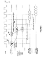
- FIG. 4 shows a timing design 400 of a buffer chip that makes a buffered stack of DRAM circuits mimic longer CAS latency DRAM to a memory controller, in accordance with another embodiment.
- the design of the buffer chip may be implemented in the context of the architecture and environment of FIGS. 1-3 .
- the design of the buffer chip may be used in any desired environment. It should also be noted that the aforementioned definitions may apply during the present description.
- any delay through a buffer chip may be made transparent to a memory controller of a host system (e.g. see the host system 204 of FIGS. 2A-E , etc.) utilizing the buffer chip.
- the buffer chip may buffer a stack of DRAM circuits such that the buffered stack of DRAM circuits appears as at least one larger capacity DRAM circuit with higher CAS latency.
- Such delay may be a result of the buffer chip being located electrically between the memory bus of the host system and the stacked DRAM circuits, since most or all of the signals that connect the memory bus to the DRAM circuits pass through the buffer chip. A finite amount of time may therefore be needed for these signals to traverse through the buffer chip.
- industry standard protocols for memory e.g. (DDR SDRAM), DDR2 SDRAM, etc.
- DDR SDRAM register chips and advanced memory buffers
- Industry standard protocols for memory e.g. (DDR SDRAM), DDR2 SDRAM, etc.
- Such industry standard protocols define the properties of a register chip and AMB but not the properties of the buffer chip 202 , etc. Thus, the signal delay through the buffer chip may violate the specifications of industry standard protocols.
- the buffer chip may provide a one-half clock cycle delay between the buffer chip receiving address and control signals from the memory, controller or optionally from a register chip, an AMB etc.) and the address and control signals being valid at the inputs of the stacked DRAM circuits.
- the data signals may also have a one-half clock cycle delay in traversing the buffer chip, either from the memory controller to the DRAM circuits or from the DRAM circuits to the memory controller.
- the one-half clock cycle delay set forth above is set forth for illustrative purposes only and thus should not be construed as limiting in any manner whatsoever.
- a one clock cycle delay, a multiple clock cycle delay (or fraction thereof), and/or any other delay amount is incorporated, for that matter.
- the aforementioned delay may be coordinated among multiple signals such that different signals are subject to time-shifting with different relative directions/magnitudes, in an organized fashion.
- the cumulative delay through the buffer chip (e.g. the sum of a first delay 402 of the address and control signals through the buffer chip and a second delay 404 of the data signals through the buffer chip) is j clock cycles.
- the buffer chip may make the buffered stack appear to the memory controller as one or more larger DRAM circuits with a CAS latency 408 of i+j clocks, where i is the native CAS latency of the DRAM circuits.
- the buffer chip may make the buffered stack appear to the memory controller as one or more larger DRAM circuits with a CAS latency of 5 (i.e. 4+1).
- the buffer chip may make the buffered stack appear as one or more larger DRAM circuits with a CAS latency of 6 (i.e. 4+2).
- FIG. 5 shows the write data timing 500 expected by a DRAM circuit in a buffered stack, in accordance with yet another embodiment.
- the write data timing 500 may be implemented in the context of the architecture and environment of FIGS. 1-4 . Of course, however, the write data timing 500 may be carried out in any desired environment. It should also be noted that the aforementioned definitions may apply during the present description.
- Designating a buffer chip (e.g. see the buffer chip 202 of FIGS. 2A-E , etc.) so that a buffered stack appears as at least one larger capacity DRAM circuit with higher CAS latency may, in some embodiments, create a problem with the timing of write operations.
- the DDR2 SDRAM protocol may specify that the write CAS latency is one less than the read CAS latency. Therefore, since the buffered stack appears as a DDR2 SDRAM with a read CAS latency of 6, the memory controller may use a write CAS latency of 5 (see 502 ) when scheduling a write operation to the buffered stack.
- the DRAM circuits may require a write CAS latency of 3 (see 504 ).
- the write data from the memory controller may arrive at the buffer chip later than when the DRAM circuits require the data.
- the buffer chip may delay such write operations to alleviate any of such timing problems. Such delay in write operations will be described in more detail with respect to FIG. 6 below.
- FIG. 6 shows write operations 600 delayed by a buffer chip, in accordance with still vet another embodiment.
- the write operations 600 may be implemented in the context of the architecture and environment of FIGS. 1-5 .
- the write operations 600 may be used in any desired environment.
- the aforementioned definitions may apply during the present description.
- a buffer chip may provide an additional delay over and beyond the delay of the address and control signals through the buffer chip, between receiving the write operation and address from the memory controller (and/or optionally from a register and/or AMB, etc.), and sending it to the DRAM circuits in the stack.
- the additional delay may be equal to j clocks, where j is the cumulative delay of the address and control signals through the butler chip and the delay of the data signals through the buffer chip.
- the write address and operation may be delayed by a register chip on a DIMM, by an AMB, or by the memory controller.
- FIG. 7 shows early write data 700 from an AMB, in accordance with another embodiment.
- the early write data 700 may be implemented in the context of the architecture and environment of FIGS. 1-5 .
- the early write data 700 may be used in any desired environment. It should also be noted that the aforementioned definitions may apply during the present description.
- an AMB on an FB-DIMM may be designed to send write data earlier to buffered stacks instead of delaying the write address and operation, as described in reference to FIG. 6 .
- an early write latency 702 may be utilized to send the write data to the buffered stack.
- correct timing of the write operation at the inputs of the DRAM circuits in the stack may be ensured.
- a buffer chip (e.g. see the buffer chip 202 of FIGS. 2A-E , etc.) may have a cumulative latency of 2, in which case, the AMB may send the write data 2 clock cycles earlier to the buffered stack. It should be noted that this scheme may not be possible in the case of registered DIMMs since the memory controller sends the write data directly to the buffered stacks. As an option, a memory controller may be designed to send write data earlier so that write operations have the correct timing at the input of the DIMM circuits in the stack without requiring the buffer chip to delay the write address and operation.
- FIG. 8 shows address bus conflicts 800 caused by delayed write operations, in accordance with yet another embodiment.
- the delaying of the write addresses and operations may be performed by a buffer chip, or optionally a register, AMB, etc., in a manner that is completely transparent to the memory controller of a host system.
- the memory controller since the memory controller is unaware of this delay, it may schedule subsequent operations, such as for example activate or precharge operations which may collide with the delayed writes on the address bus from the buffer chip to the DRAM circuits in the stack.
- an activate operation 802 may interfere with a write operation 804 that has been delayed.
- a delay of activate operations may be employed, as will be described in further detail with respect to FIG. 9 .
- FIGS. 9A-B show variable delays 900 and 950 of operations through a buffer chip, in accordance with anther embodiment.
- the variable delays 900 and 950 may be implemented in the context of the architecture and environment of FIGS. 1-8 .
- the variable delays 900 and 950 may be carried out in any desired environment. It should also be noted that the aforementioned definitions may apply during the present description.
- either the write operation or the precharge/activate operation may be delayed.
- a buffer chip e.g. see the buffer chip 202 of FIGS. 2A-E , etc.
- the buffer chip may make the buffered stack appear as one or more larger capacity DRAM circuits that have longer tRCD (RAS to CAS delay) and tRP (i.e. precharge time) parameters.
- the buffered stack may appear as one or more larger capacity DRAM circuits with a read CAS latency of 6 clock cycles to the memory controller.
- the buffered stack may appear as one or more larger capacity DRAM circuits with tRCD of 6 clock cycles and tRP of 6 clock cycles in order to allow a buffer chip (e.g., see the buffer chip 202 of FIGS.
- the memory controller may schedule a column operation to a bank 6 clock cycles after an activate (e.g. row) operation to the same bank.
- the DRAMA circuits in the stack may actually have a tRCD of 4 clock cycles.
- the buffer chip may have the ability to delay the activate operation by up to 2 clock cycles in order to avoid any conflicts on the address bus between the buffer chip and the DRAM circuits in the stack while still ensuring correct read and write timing on the channel between the memory controller and the buffered stack.
- the buffer chip may issue the activate operation to the DRAM circuits one, two, or three clock cycles after it receives the activate operation front the memory controller, register, or AMB.
- the actual delay of the activate operation through the buffer chip may depend on the presence or absence of other DRAM operations that may conflict with the activate operation, and may optionally change from one activate operation to another.
- the buffered stack may appear to the memory controller as at least one larger capacity DRAM circuit with a tRP of 6 clock cycles, the memory controller may schedule a subsequent activate (e.g. row) operation to a bank a minimum of 6 clock cycles after issuing a precharge operation to that bank.
- the buffer chip may have the ability to delay issuing the precharge operation to the DRAM circuits in the stack by up to 2 clock cycles in order to avoid any conflicts on the address bus between the buffer chip and the DRAM circuits in the stack.
- the buffer chip may still delay issuing a precharge operation in order to satisfy the tRAS requirement of the DRAMA circuits.
- the precharge operation to the same bank may be delayed by the buffer chip to satisfy the tRAS requirement of the DRAM circuits.
- the buffer chip may issue the precharge operation to the DRAM circuits one, two, or three clock cycles after it receives the precharge operation from the memory controller, register, or AMB.
- the actual delay of the precharge operation through the buffer chip may depend on the presence or absence of address bus conflicts or tRAS violations, and may change from one precharge operation to another.
- FIG. 10 shows a buffered stack 1000 of four 512 Mb DRAM circuits mapped to a single 2 Gb DRAM circuit, in accordance with yet another embodiment.
- the buffered stack 1000 may be implemented in the context of the architecture and environment of FIGS. 1-9 .
- the buffered stack 1000 may be carried out in any desired environment. It should also be noted that the aforementioned definitions may apply during the present description.
- the multiple DRAM circuits 1002 A-D buffered in the stack by the buffer chip 1004 may appear as at least one larger capacity DRAM circuit to the memory controller.
- the combined power dissipation of such DRAM circuits 1002 A-D may be much higher than the power dissipation of a monolithic DRAM of the same capacity.
- the buffered stack may consist of four 512 Mb DDR2 SDRAM circuits that appear to the memory controller as a single 2 Gb DDR2 SDRAM circuit.
- the power dissipation of all four DRAM circuits 1002 A-D in the stack may be much higher than the power dissipation of a monolithic 2 Gb DDR2 SDRAM.
- a DIMM containing multiple buffered stacks may dissipate much more power than a standard DIMM built using monolithic DRAM circuits. This increased power dissipation may limit the widespread adoption of DIMMs that use buffered stacks.
- the DRAM circuits 1002 A-D may be opportunistically placed in a precharge power down mode using the clock enable (CKE) pin of the DRAM circuits 1002 A-D.
- CKE clock enable
- a single rank registered DIMM R-DIMM
- R-DIMM may contain a plurality of buffered stacks of DRAM circuits 1002 A-D, where each stack consists of four ⁇ 4 512 Mb DDR2 SDRAM circuits 1002 A-D and appears as a single ⁇ 4 2 Gb DDR2 SDRAM circuit to the memory controller.
- a 2 Gb DDR2 SDRAM may generally have eight banks as specified by JEDEC. Therefore, the buffer chip 1004 may map each 512 Mb DRAM circuit in the stack to two banks of the equivalent 2 Gb DRAM, as shown.
- the memory controller of the host system may open and close pages in the banks of the DRAM circuits 1002 A-D based on the memory requests it receives from the rest of the system.
- no more than one page may be able to be open in a bank at any given time.
- a DRAM circuit 1002 A-D since each DRAM circuit 1002 A-D in the stack is mapped to two banks of the equivalent lamer DRAM, at any given time a DRAM circuit 1002 A-D may have two open pages, one open page, or no open pages.
- the power management scheme may place that DRAM circuit 1002 A-D in the precharge power down mode by de-asserting its CKE input.
- the CKE inputs of the DRAM circuits 1002 A-D in a stack may be controlled by the buffer chip 1004 , by a chip on an R-DIMM, by an AMB on a FB-DIMM, or by the memory controller in order to implement the power management scheme described hereinabove.
- this power management scheme may be particularly efficient when the memory controller implements a closed page policy.
- Another optional power management scheme may include mapping a plurality of DRAM circuits to a single bank of the larger capacity DRAM seen by the memory controller. For example, a buffered stack of sixteen ⁇ 4 256 Mb DDR2 SDRAM circuits may appear to the memory controller as a single ⁇ 4 4 Gb DDR2 SDRAM circuit. Since a 4 Gb DDR2 SDRAM circuit is specified by JEDEC to have eight banks, each bank of the 4 Gb DDR2 SDRAM circuit may be 512 Mb. Thus, two of the 256 Mb DDR2 SDRAM circuits may be mapped by the buffer chip 1004 to a single bank of the equivalent 4 Gb DDR2 SDRAM circuit seen by the controller.
- bank 0 of the 4 Gb DDR2 SDRAM circuit may be mapped by the buffer chip to two 256 Mb DDR2 SDRAM circuits (e.g. DRAM A and DRAM B) in the stack.
- DRAM A and DRAM B 256 Mb DDR2 SDRAM circuits
- DRAM B may be placed in the precharge power down mode by de-asserting its CKE input.
- DRAM A may be placed in the precharge power down mode by de-asserting its CKE input.
- This technique may ensure that if p DRAM circuits are mapped to a bank of the larger capacity DRAM circuit seen by the memory controller, then p-l of the p DRAM circuits may continuously (e.g. always, etc.) be subjected to a power saving operation.
- the power saving operation may, for example, comprise operating in precharge power down mode except when refresh is required.
- power-savings may also occur in other embodiments without such continuity.
- FIG. 11 illustrates a method 1100 for refreshing a plurality of memory circuits, in accordance with still yet another embodiment.
- the method 1100 may be implemented in the context of the architecture and environment of any one or more of FIGS. 1-10 .
- the method 1100 may be carried out by the interface circuit 102 of FIG. 1 .
- the method 1100 may be carried out in any desired environment. It should also be noted that the aforementioned definitions may apply during the present description.
- a refresh control signal is received in operation 1102 .
- such refresh control signal may, for example, be received from a memory controller, where such memory controller intends to refresh a simulated memory circuit(s).
- a plurality of refresh control signals are sent to a plurality of the memory circuits (e.g. see the memory circuits 104 A, 104 B, 104 N of FIG. 1 , etc.), at different times. See operation 1104 .
- Such refresh control signals may or may not each include the refresh control signal of operation 1102 or an instantiation/copy thereof.
- the refresh control signals may each include refresh control signals that are different in at least one aspect (e.g. format, content, etc.).
- At least one first refresh control signal may be sent to a first subset (e.g. of one or more) of the memory circuits at a first time and at least one second refresh control signal may be sent to a second subset (e.g. of one or more) of the memory circuits at a second time.
- a single refresh control signal may be sent to a plurality of the memory circuits (e.g. a group of memory circuits, etc.).
- a plurality, of the refresh control signals may be sent to a plurality of the memory circuits.
- refresh control signals may be sent individually or to groups of memory circuits, as desired.
- the refresh control signals may be sent after a delay in accordance with a particular timing.
- the timing in which the refresh control signals are sent to the memory circuits may, be selected to minimize a current draw. This may be accomplished in various embodiments by staggering a plurality of refresh control signals.
- the timing in which the refresh control signals are sent to the memory circuits may be selected to comply with a tRFC parameter associated with each of the memory circuits.
- DRAM circuits of any desired size may receive periodic refresh operations to maintain the integrity of data therein.
- a memory controller may initiate refresh operations by issuing refresh control signals to the DRAM circuits with sufficient frequency to prevent any loss of data in the DRAM circuits.
- a refresh control signal is issued to a DRAM circuit a minimum time (e.g. denoted by tRFC) may be required to elapse before another control signal may be issued to that DRAM circuit.
- the tRFC parameter may therefore increase as the size of the DRAM circuit increases.
- the buffer chip When the buffer chip receives a refresh control signal from the memory controller, it may refresh the smaller DRAM circuits within the span of time specified by the tRFC associated with the emulated DRAM circuit. Since the tRFC of the emulated DRAM circuits is larger than that of the smaller DRAM circuits, it may not be necessary to issue refresh control signals to all of the smaller DRAM circuits simultaneously. Refresh control signals may be issued separately to individual DRAM circuits or may be is sued to groups of DRAM circuits, provided that the tRFC requirement of the smaller DRAM circuits is satisfied by the time the tRFC of the emulated DRAM circuits has elapsed. In use, the refreshes may be spaced to minimize the peak current draw of the combination buffer chip and DRAM circuit set during a refresh operation.
Abstract
Description
Claims (23)
Priority Applications (2)
| Application Number | Priority Date | Filing Date | Title |
|---|---|---|---|
| US11/461,430 US7724589B2 (en) | 2006-07-31 | 2006-07-31 | System and method for delaying a signal communicated from a system to at least one of a plurality of memory circuits |
| US12/769,428 US8154935B2 (en) | 2006-07-31 | 2010-04-28 | Delaying a signal communicated from a system to at least one of a plurality of memory circuits |
Applications Claiming Priority (1)
| Application Number | Priority Date | Filing Date | Title |
|---|---|---|---|
| US11/461,430 US7724589B2 (en) | 2006-07-31 | 2006-07-31 | System and method for delaying a signal communicated from a system to at least one of a plurality of memory circuits |
Related Child Applications (1)
| Application Number | Title | Priority Date | Filing Date |
|---|---|---|---|
| US12/769,428 Continuation US8154935B2 (en) | 2006-07-31 | 2010-04-28 | Delaying a signal communicated from a system to at least one of a plurality of memory circuits |
Publications (2)
| Publication Number | Publication Date |
|---|---|
| US20080025108A1 US20080025108A1 (en) | 2008-01-31 |
| US7724589B2 true US7724589B2 (en) | 2010-05-25 |
Family
ID=38986089
Family Applications (2)
| Application Number | Title | Priority Date | Filing Date |
|---|---|---|---|
| US11/461,430 Active US7724589B2 (en) | 2006-07-31 | 2006-07-31 | System and method for delaying a signal communicated from a system to at least one of a plurality of memory circuits |
| US12/769,428 Active US8154935B2 (en) | 2006-07-31 | 2010-04-28 | Delaying a signal communicated from a system to at least one of a plurality of memory circuits |
Family Applications After (1)
| Application Number | Title | Priority Date | Filing Date |
|---|---|---|---|
| US12/769,428 Active US8154935B2 (en) | 2006-07-31 | 2010-04-28 | Delaying a signal communicated from a system to at least one of a plurality of memory circuits |
Country Status (1)
| Country | Link |
|---|---|
| US (2) | US7724589B2 (en) |
Cited By (44)
| Publication number | Priority date | Publication date | Assignee | Title |
|---|---|---|---|---|
| US20090290442A1 (en) * | 2005-06-24 | 2009-11-26 | Rajan Suresh N | Method and circuit for configuring memory core integrated circuit dies with memory interface integrated circuit dies |
| US20100257304A1 (en) * | 2006-07-31 | 2010-10-07 | Google Inc. | Apparatus and method for power management of memory circuits by a system or component thereof |
| US8019589B2 (en) | 2006-07-31 | 2011-09-13 | Google Inc. | Memory apparatus operable to perform a power-saving operation |
| US8055833B2 (en) | 2006-10-05 | 2011-11-08 | Google Inc. | System and method for increasing capacity, performance, and flexibility of flash storage |
| US8060774B2 (en) | 2005-06-24 | 2011-11-15 | Google Inc. | Memory systems and memory modules |
| US8077535B2 (en) | 2006-07-31 | 2011-12-13 | Google Inc. | Memory refresh apparatus and method |
| US8080874B1 (en) | 2007-09-14 | 2011-12-20 | Google Inc. | Providing additional space between an integrated circuit and a circuit board for positioning a component therebetween |
| US8081474B1 (en) | 2007-12-18 | 2011-12-20 | Google Inc. | Embossed heat spreader |
| US8090897B2 (en) | 2006-07-31 | 2012-01-03 | Google Inc. | System and method for simulating an aspect of a memory circuit |
| US8089795B2 (en) | 2006-02-09 | 2012-01-03 | Google Inc. | Memory module with memory stack and interface with enhanced capabilities |
| US8111566B1 (en) | 2007-11-16 | 2012-02-07 | Google, Inc. | Optimal channel design for memory devices for providing a high-speed memory interface |
| US8130560B1 (en) | 2006-11-13 | 2012-03-06 | Google Inc. | Multi-rank partial width memory modules |
| US8154935B2 (en) | 2006-07-31 | 2012-04-10 | Google Inc. | Delaying a signal communicated from a system to at least one of a plurality of memory circuits |
| US8169233B2 (en) | 2009-06-09 | 2012-05-01 | Google Inc. | Programming of DIMM termination resistance values |
| US8181048B2 (en) | 2006-07-31 | 2012-05-15 | Google Inc. | Performing power management operations |
| US8209479B2 (en) | 2007-07-18 | 2012-06-26 | Google Inc. | Memory circuit system and method |
| US8213205B2 (en) | 2005-09-02 | 2012-07-03 | Google Inc. | Memory system including multiple memory stacks |
| US8244971B2 (en) | 2006-07-31 | 2012-08-14 | Google Inc. | Memory circuit system and method |
| US8280714B2 (en) | 2006-07-31 | 2012-10-02 | Google Inc. | Memory circuit simulation system and method with refresh capabilities |
| US8327104B2 (en) | 2006-07-31 | 2012-12-04 | Google Inc. | Adjusting the timing of signals associated with a memory system |
| US8335894B1 (en) | 2008-07-25 | 2012-12-18 | Google Inc. | Configurable memory system with interface circuit |
| US8386722B1 (en) | 2008-06-23 | 2013-02-26 | Google Inc. | Stacked DIMM memory interface |
| US8397013B1 (en) | 2006-10-05 | 2013-03-12 | Google Inc. | Hybrid memory module |
| US8438328B2 (en) | 2008-02-21 | 2013-05-07 | Google Inc. | Emulation of abstracted DIMMs using abstracted DRAMs |
| US8566516B2 (en) | 2006-07-31 | 2013-10-22 | Google Inc. | Refresh management of memory modules |
| US8796830B1 (en) | 2006-09-01 | 2014-08-05 | Google Inc. | Stackable low-profile lead frame package |
| US8909874B2 (en) | 2012-02-13 | 2014-12-09 | International Business Machines Corporation | Memory reorder queue biasing preceding high latency operations |
| US8930647B1 (en) | 2011-04-06 | 2015-01-06 | P4tents1, LLC | Multiple class memory systems |
| US8949519B2 (en) | 2005-06-24 | 2015-02-03 | Google Inc. | Simulating a memory circuit |
| US9123441B1 (en) | 2014-04-04 | 2015-09-01 | Inphi Corporation | Backward compatible dynamic random access memory device and method of testing therefor |
| US9158546B1 (en) | 2011-04-06 | 2015-10-13 | P4tents1, LLC | Computer program product for fetching from a first physical memory between an execution of a plurality of threads associated with a second physical memory |
| US9164679B2 (en) | 2011-04-06 | 2015-10-20 | Patents1, Llc | System, method and computer program product for multi-thread operation involving first memory of a first memory class and second memory of a second memory class |
| US9171585B2 (en) | 2005-06-24 | 2015-10-27 | Google Inc. | Configurable memory circuit system and method |
| US9170744B1 (en) | 2011-04-06 | 2015-10-27 | P4tents1, LLC | Computer program product for controlling a flash/DRAM/embedded DRAM-equipped system |
| US9176671B1 (en) | 2011-04-06 | 2015-11-03 | P4tents1, LLC | Fetching data between thread execution in a flash/DRAM/embedded DRAM-equipped system |
| US9417754B2 (en) | 2011-08-05 | 2016-08-16 | P4tents1, LLC | User interface system, method, and computer program product |
| US9507739B2 (en) | 2005-06-24 | 2016-11-29 | Google Inc. | Configurable memory circuit system and method |
| US9520168B2 (en) * | 2013-01-18 | 2016-12-13 | Samsung Electronics Co., Ltd. | Nonvolatile memory devices, memory systems and related control methods |
| US9542352B2 (en) | 2006-02-09 | 2017-01-10 | Google Inc. | System and method for reducing command scheduling constraints of memory circuits |
| US9632954B2 (en) | 2011-11-07 | 2017-04-25 | International Business Machines Corporation | Memory queue handling techniques for reducing impact of high-latency memory operations |
| US9632929B2 (en) | 2006-02-09 | 2017-04-25 | Google Inc. | Translating an address associated with a command communicated between a system and memory circuits |
| US10013371B2 (en) | 2005-06-24 | 2018-07-03 | Google Llc | Configurable memory circuit system and method |
| US20180226412A1 (en) * | 2013-12-05 | 2018-08-09 | Taiwan Semiconductor Manufacturing Company, Ltd. | Three-Dimensional Static Random Access Memory Device Structures |
| US10198187B1 (en) | 2015-10-16 | 2019-02-05 | Rambus Inc. | Buffering device with status communication method for memory controller |
Families Citing this family (14)
| Publication number | Priority date | Publication date | Assignee | Title |
|---|---|---|---|---|
| US7590796B2 (en) * | 2006-07-31 | 2009-09-15 | Metaram, Inc. | System and method for power management in memory systems |
| US7580312B2 (en) * | 2006-07-31 | 2009-08-25 | Metaram, Inc. | Power saving system and method for use with a plurality of memory circuits |
| US7392338B2 (en) * | 2006-07-31 | 2008-06-24 | Metaram, Inc. | Interface circuit system and method for autonomously performing power management operations in conjunction with a plurality of memory circuits |
| US20080028137A1 (en) * | 2006-07-31 | 2008-01-31 | Schakel Keith R | Method and Apparatus For Refresh Management of Memory Modules |
| US20080025136A1 (en) * | 2006-07-31 | 2008-01-31 | Metaram, Inc. | System and method for storing at least a portion of information received in association with a first operation for use in performing a second operation |
| US20090103373A1 (en) * | 2007-10-19 | 2009-04-23 | Uniram Technology Inc. | High performance high capacity memory systems |
| KR101796116B1 (en) | 2010-10-20 | 2017-11-10 | 삼성전자 주식회사 | Semiconductor device, memory module and memory system having the same and operating method thereof |
| TWI433296B (en) * | 2010-11-19 | 2014-04-01 | Ind Tech Res Inst | Multi-chip stacked system and chip select apparatus thereof |
| US8976610B2 (en) | 2012-10-11 | 2015-03-10 | Everspin Technologies, Inc. | Memory device with timing overlap mode |
| US9251048B2 (en) | 2012-10-19 | 2016-02-02 | International Business Machines Corporation | Memory page management |
| KR102094309B1 (en) * | 2013-12-30 | 2020-03-27 | 에스케이하이닉스 주식회사 | Stacked semiconductor appatus to generate refresh signal |
| KR20170077605A (en) * | 2015-12-28 | 2017-07-06 | 에스케이하이닉스 주식회사 | Memory module and memory system including the same |
| US11054992B2 (en) | 2015-12-28 | 2021-07-06 | SK Hynix Inc. | Memory module and memory system including the memory module |
| US10679722B2 (en) | 2016-08-26 | 2020-06-09 | Sandisk Technologies Llc | Storage system with several integrated components and method for use therewith |
Citations (389)
| Publication number | Priority date | Publication date | Assignee | Title |
|---|---|---|---|---|
| US4334307A (en) | 1979-12-28 | 1982-06-08 | Honeywell Information Systems Inc. | Data processing system with self testing and configuration mapping capability |
| US4345319A (en) | 1978-06-28 | 1982-08-17 | Cselt-Centro Studi E Laboratori Telecomunicazioni S.P.A. | Self-correcting, solid-state-mass-memory organized by bits and with reconfiguration capability for a stored program control system |
| US4392212A (en) | 1979-11-12 | 1983-07-05 | Fujitsu Limited | Semiconductor memory device with decoder for chip selection/write in |
| US4525921A (en) | 1981-07-13 | 1985-07-02 | Irvine Sensors Corporation | High-density electronic processing package-structure and fabrication |
| US4646128A (en) | 1980-09-16 | 1987-02-24 | Irvine Sensors Corporation | High-density electronic processing package--structure and fabrication |
| US4698748A (en) | 1983-10-07 | 1987-10-06 | Essex Group, Inc. | Power-conserving control system for turning-off the power and the clocking for data transactions upon certain system inactivity |
| US4706166A (en) | 1986-04-25 | 1987-11-10 | Irvine Sensors Corporation | High-density electronic modules--process and product |
| US4710903A (en) | 1986-03-31 | 1987-12-01 | Wang Laboratories, Inc. | Pseudo-static memory subsystem |
| US4764846A (en) | 1987-01-05 | 1988-08-16 | Irvine Sensors Corporation | High density electronic package comprising stacked sub-modules |
| US4780843A (en) | 1983-11-07 | 1988-10-25 | Motorola, Inc. | Wait mode power reduction system and method for data processor |
| US4794597A (en) | 1986-03-28 | 1988-12-27 | Mitsubishi Denki Kabushiki Kaisha | Memory device equipped with a RAS circuit |
| US4796232A (en) | 1987-10-20 | 1989-01-03 | Contel Corporation | Dual port memory controller |
| US4841440A (en) | 1983-04-26 | 1989-06-20 | Nec Corporation | Control processor for controlling a peripheral unit |
| US4862347A (en) | 1986-04-22 | 1989-08-29 | International Business Machine Corporation | System for simulating memory arrays in a logic simulation machine |
| US4884237A (en) | 1984-03-28 | 1989-11-28 | International Business Machines Corporation | Stacked double density memory module using industry standard memory chips |
| US4887240A (en) | 1987-12-15 | 1989-12-12 | National Semiconductor Corporation | Staggered refresh for dram array |
| US4899107A (en) | 1988-09-30 | 1990-02-06 | Micron Technology, Inc. | Discrete die burn-in for nonpackaged die |
| US4922451A (en) | 1987-03-23 | 1990-05-01 | International Business Machines Corporation | Memory re-mapping in a microcomputer system |
| US4982265A (en) | 1987-06-24 | 1991-01-01 | Hitachi, Ltd. | Semiconductor integrated circuit device and method of manufacturing the same |
| US4983533A (en) | 1987-10-28 | 1991-01-08 | Irvine Sensors Corporation | High-density electronic modules - process and product |
| US5072424A (en) | 1985-07-12 | 1991-12-10 | Anamartic Limited | Wafer-scale integrated circuit memory |
| US5083266A (en) | 1986-12-26 | 1992-01-21 | Kabushiki Kaisha Toshiba | Microcomputer which enters sleep mode for a predetermined period of time on response to an activity of an input/output device |
| US5104820A (en) | 1989-07-07 | 1992-04-14 | Irvine Sensors Corporation | Method of fabricating electronic circuitry unit containing stacked IC layers having lead rerouting |
| US5220672A (en) | 1990-12-25 | 1993-06-15 | Mitsubishi Denki Kabushiki Kaisha | Low power consuming digital circuit device |
| US5241266A (en) | 1992-04-10 | 1993-08-31 | Micron Technology, Inc. | Built-in test circuit connection for wafer level burnin and testing of individual dies |
| US5332922A (en) | 1990-04-26 | 1994-07-26 | Hitachi, Ltd. | Multi-chip semiconductor package |
| US5347428A (en) | 1992-12-03 | 1994-09-13 | Irvine Sensors Corporation | Module comprising IC memory stack dedicated to and structurally combined with an IC microprocessor chip |
| US5388265A (en) | 1992-03-06 | 1995-02-07 | Intel Corporation | Method and apparatus for placing an integrated circuit chip in a reduced power consumption state |
| US5408190A (en) | 1991-06-04 | 1995-04-18 | Micron Technology, Inc. | Testing apparatus having substrate interconnect for discrete die burn-in for nonpackaged die |
| US5432729A (en) | 1993-04-23 | 1995-07-11 | Irvine Sensors Corporation | Electronic module comprising a stack of IC chips each interacting with an IC chip secured to the stack |
| US5448511A (en) | 1994-06-01 | 1995-09-05 | Storage Technology Corporation | Memory stack with an integrated interconnect and mounting structure |
| US5498886A (en) | 1991-11-05 | 1996-03-12 | Monolithic System Technology, Inc. | Circuit module redundancy architecture |
| US5502667A (en) | 1993-09-13 | 1996-03-26 | International Business Machines Corporation | Integrated multichip memory module structure |
| US5502333A (en) | 1994-03-30 | 1996-03-26 | International Business Machines Corporation | Semiconductor stack structures and fabrication/sparing methods utilizing programmable spare circuit |
| US5513135A (en) | 1994-12-02 | 1996-04-30 | International Business Machines Corporation | Synchronous memory packaged in single/dual in-line memory module and method of fabrication |
| US5519832A (en) | 1992-11-13 | 1996-05-21 | Digital Equipment Corporation | Method and apparatus for displaying module diagnostic results |
| US5561622A (en) | 1993-09-13 | 1996-10-01 | International Business Machines Corporation | Integrated memory cube structure |
| US5581498A (en) | 1993-08-13 | 1996-12-03 | Irvine Sensors Corporation | Stack of IC chips in lieu of single IC chip |
| US5590071A (en) | 1995-11-16 | 1996-12-31 | International Business Machines Corporation | Method and apparatus for emulating a high capacity DRAM |
| US5654204A (en) | 1994-07-20 | 1997-08-05 | Anderson; James C. | Die sorter |
| US5680342A (en) | 1996-04-10 | 1997-10-21 | International Business Machines Corporation | Memory module package with address bus buffering |
| US5692121A (en) | 1995-04-14 | 1997-11-25 | International Business Machines Corporation | Recovery unit for mirrored processors |
| US5692202A (en) | 1995-12-29 | 1997-11-25 | Intel Corporation | System, apparatus, and method for managing power in a computer system |
| US5729504A (en) | 1995-12-14 | 1998-03-17 | Micron Technology, Inc. | Continuous burst edo memory device |
| US5742792A (en) | 1993-04-23 | 1998-04-21 | Emc Corporation | Remote data mirroring |
| US5748914A (en) | 1995-10-19 | 1998-05-05 | Rambus, Inc. | Protocol for communication with dynamic memory |
| US5752045A (en) | 1995-07-14 | 1998-05-12 | United Microelectronics Corporation | Power conservation in synchronous SRAM cache memory blocks of a computer system |
| US5761703A (en) | 1996-08-16 | 1998-06-02 | Unisys Corporation | Apparatus and method for dynamic memory refresh |
| US5781766A (en) | 1996-05-13 | 1998-07-14 | National Semiconductor Corporation | Programmable compensating device to optimize performance in a DRAM controller chipset |
| US5802555A (en) | 1995-03-15 | 1998-09-01 | Texas Instruments Incorporated | Computer system including a refresh controller circuit having a row address strobe multiplexer and associated method |
| US5835435A (en) | 1997-12-02 | 1998-11-10 | Intel Corporation | Method and apparatus for dynamically placing portions of a memory in a reduced power consumtion state |
| US5841580A (en) | 1990-04-18 | 1998-11-24 | Rambus, Inc. | Integrated circuit I/O using a high performance bus interface |
| US5843807A (en) | 1993-03-29 | 1998-12-01 | Staktek Corporation | Method of manufacturing an ultra-high density warp-resistant memory module |
| US5845108A (en) | 1995-12-22 | 1998-12-01 | Samsung Electronics, Co., Ltd. | Semiconductor memory device using asynchronous signal |
| US5860106A (en) | 1995-07-13 | 1999-01-12 | Intel Corporation | Method and apparatus for dynamically adjusting power/performance characteristics of a memory subsystem |
| US5870350A (en) | 1997-05-21 | 1999-02-09 | International Business Machines Corporation | High performance, high bandwidth memory bus architecture utilizing SDRAMs |
| US5872907A (en) | 1991-12-16 | 1999-02-16 | International Business Machines Corporation | Fault tolerant design for identification of AC defects including variance of cycle time to maintain system operation |
| US5901105A (en) | 1995-04-05 | 1999-05-04 | Ong; Adrian E | Dynamic random access memory having decoding circuitry for partial memory blocks |
| US5905688A (en) | 1997-04-01 | 1999-05-18 | Lg Semicon Co., Ltd. | Auto power down circuit for a semiconductor memory device |
| US5915167A (en) | 1997-04-04 | 1999-06-22 | Elm Technology Corporation | Three dimensional structure memory |
| US5929650A (en) | 1997-02-04 | 1999-07-27 | Motorola, Inc. | Method and apparatus for performing operative testing on an integrated circuit |
| US5943254A (en) | 1995-02-22 | 1999-08-24 | International Business Machines Corporation | Multichip semiconductor structures with consolidated circuitry and programmable ESD protection for input/output nodes |
| US5953215A (en) | 1997-12-01 | 1999-09-14 | Karabatsos; Chris | Apparatus and method for improving computer memory speed and capacity |
| US5956233A (en) | 1997-12-19 | 1999-09-21 | Texas Instruments Incorporated | High density single inline memory module |
| US5963464A (en) | 1998-02-26 | 1999-10-05 | International Business Machines Corporation | Stackable memory card |
| US5966727A (en) | 1996-07-12 | 1999-10-12 | Dux Inc. | Combination flash memory and dram memory board interleave-bypass memory access method, and memory access device incorporating both the same |
| US5969996A (en) | 1995-04-25 | 1999-10-19 | Hiachi, Ltd. | Semiconductor memory device and memory system |
| US5973392A (en) | 1997-04-02 | 1999-10-26 | Nec Corporation | Stacked carrier three-dimensional memory module and semiconductor device using the same |
| US5995424A (en) | 1997-07-16 | 1999-11-30 | Tanisys Technology, Inc. | Synchronous memory test system |
| US6014339A (en) | 1997-04-03 | 2000-01-11 | Fujitsu Limited | Synchronous DRAM whose power consumption is minimized |
| US6026050A (en) | 1997-07-09 | 2000-02-15 | Micron Technology, Inc. | Method and apparatus for adaptively adjusting the timing of a clock signal used to latch digital signals, and memory device using same |
| US6029250A (en) | 1998-09-09 | 2000-02-22 | Micron Technology, Inc. | Method and apparatus for adaptively adjusting the timing offset between a clock signal and digital signals transmitted coincident with that clock signal, and memory device and system using same |
| US6038673A (en) | 1998-11-03 | 2000-03-14 | Intel Corporation | Computer system with power management scheme for DRAM devices |
| US6047344A (en) | 1997-03-05 | 2000-04-04 | Kabushiki Kaisha Toshiba | Semiconductor memory device with multiplied internal clock |
| US6047073A (en) | 1994-11-02 | 2000-04-04 | Advanced Micro Devices, Inc. | Digital wavetable audio synthesizer with delay-based effects processing |
| US6053948A (en) | 1995-06-07 | 2000-04-25 | Synopsys, Inc. | Method and apparatus using a memory model |
| US6070217A (en) | 1996-07-08 | 2000-05-30 | International Business Machines Corporation | High density memory module with in-line bus switches being enabled in response to read/write selection state of connected RAM banks to improve data bus performance |
| US6073223A (en) | 1997-07-21 | 2000-06-06 | Hewlett-Packard Company | Memory controller and method for intermittently activating and idling a clock signal for a synchronous memory |
| US6075744A (en) | 1997-10-10 | 2000-06-13 | Rambus Inc. | Dram core refresh with reduced spike current |
| US6075730A (en) | 1997-10-10 | 2000-06-13 | Rambus Incorporated | High performance cost optimized memory with delayed memory writes |
| US6079025A (en) | 1990-06-01 | 2000-06-20 | Vadem | System and method of computer operating mode control for power consumption reduction |
| US6088290A (en) | 1997-08-13 | 2000-07-11 | Kabushiki Kaisha Toshiba | Semiconductor memory device having a power-down mode |
| US6091251A (en) | 1991-06-04 | 2000-07-18 | Wood; Alan G. | Discrete die burn-in for nonpackaged die |
| US6101197A (en) * | 1997-09-18 | 2000-08-08 | Micron Technology, Inc. | Method and apparatus for adjusting the timing of signals over fine and coarse ranges |
| US6111812A (en) | 1999-07-23 | 2000-08-29 | Micron Technology, Inc. | Method and apparatus for adjusting control signal timing in a memory device |
| USRE36839E (en) | 1995-02-14 | 2000-08-29 | Philips Semiconductor, Inc. | Method and apparatus for reducing power consumption in digital electronic circuits |
| US6134638A (en) | 1997-08-13 | 2000-10-17 | Compaq Computer Corporation | Memory controller supporting DRAM circuits with different operating speeds |
| US6154370A (en) | 1998-07-21 | 2000-11-28 | Lucent Technologies Inc. | Recessed flip-chip package |
| US6166991A (en) | 1999-11-03 | 2000-12-26 | Cypress Semiconductor Corp. | Circuit, architecture and method for reducing power consumption in a synchronous integrated circuit |
| US6216246B1 (en) | 1996-05-24 | 2001-04-10 | Jeng-Jye Shau | Methods to make DRAM fully compatible with SRAM using error correction code (ECC) mechanism |
| US6222739B1 (en) | 1998-01-20 | 2001-04-24 | Viking Components | High-density computer module with stacked parallel-plane packaging |
| US6233192B1 (en) | 1998-03-05 | 2001-05-15 | Sharp Kabushiki Kaisha | Semiconductor memory device |
| US6240048B1 (en) | 1999-06-29 | 2001-05-29 | Nec Corporation | Synchronous type semiconductor memory system with less power consumption |
| US6252807B1 (en) | 1999-08-06 | 2001-06-26 | Mitsubishi Electric Engineering Company, Limited | Memory device with reduced power consumption when byte-unit accessed |
| US6274395B1 (en) | 1999-12-23 | 2001-08-14 | Lsi Logic Corporation | Method and apparatus for maintaining test data during fabrication of a semiconductor wafer |
| US6279069B1 (en) | 1996-12-26 | 2001-08-21 | Intel Corporation | Interface for flash EEPROM memory arrays |
| US6282210B1 (en) * | 1998-08-12 | 2001-08-28 | Staktek Group L.P. | Clock driver with instantaneously selectable phase and method for use in data communication systems |
| US20010021106A1 (en) | 1999-01-14 | 2001-09-13 | Rick Weber | Stacked printed circuit board memory module |
| US20010021137A1 (en) | 2000-03-13 | 2001-09-13 | Yasukazu Kai | Dynamic random access memory |
| US6298426B1 (en) | 1997-12-31 | 2001-10-02 | Intel Corporation | Controller configurable for use with multiple memory organizations |
| US6307769B1 (en) | 1999-09-02 | 2001-10-23 | Micron Technology, Inc. | Semiconductor devices having mirrored terminal arrangements, devices including same, and methods of testing such semiconductor devices |
| US6317381B1 (en) | 1999-12-07 | 2001-11-13 | Micron Technology, Inc. | Method and system for adaptively adjusting control signal timing in a memory device |
| US6317352B1 (en) | 2000-09-18 | 2001-11-13 | Intel Corporation | Apparatus for implementing a buffered daisy chain connection between a memory controller and memory modules |
| US6327664B1 (en) | 1999-04-30 | 2001-12-04 | International Business Machines Corporation | Power management on a memory card having a signal processing element |
| US6338113B1 (en) | 1998-06-10 | 2002-01-08 | Mitsubishi Denki Kabushiki Kaisha | Memory module system having multiple memory modules |
| US20020004897A1 (en) | 2000-07-05 | 2002-01-10 | Min-Cheng Kao | Data processing apparatus for executing multiple instruction sets |
| US6341347B1 (en) | 1999-05-11 | 2002-01-22 | Sun Microsystems, Inc. | Thread switch logic in a multiple-thread processor |
| US20020015340A1 (en) | 2000-07-03 | 2002-02-07 | Victor Batinovich | Method and apparatus for memory module circuit interconnection |
| US20020019961A1 (en) | 1998-08-28 | 2002-02-14 | Blodgett Greg A. | Device and method for repairing a semiconductor memory |
| US6353561B1 (en) | 1998-09-18 | 2002-03-05 | Fujitsu Limited | Semiconductor integrated circuit and method for controlling the same |
| US6356500B1 (en) | 2000-08-23 | 2002-03-12 | Micron Technology, Inc. | Reduced power DRAM device and method |
| US20020038405A1 (en) | 1998-09-30 | 2002-03-28 | Michael W. Leddige | Method and apparatus for implementing multiple memory buses on a memory module |
| US20020041507A1 (en) | 2000-10-10 | 2002-04-11 | Woo Steven C. | Methods and systems for reducing heat flux in memory systems |
| US20020051398A1 (en) | 2000-09-12 | 2002-05-02 | Seiko Epson Corporation | Semiconductor device, method for refreshing the same, system memory, and electronics apparatus |
| US6392304B1 (en) | 1998-11-12 | 2002-05-21 | United Memories, Inc. | Multi-chip memory apparatus and associated method |
| US20020064073A1 (en) | 2000-11-30 | 2002-05-30 | Pien Chien | Dram module and method of using sram to replace damaged dram cell |
| US6414868B1 (en) | 1999-06-07 | 2002-07-02 | Sun Microsystems, Inc. | Memory expansion module including multiple memory banks and a bank control circuit |
| US20020089831A1 (en) | 2001-01-09 | 2002-07-11 | Forthun John A. | Module with one side stacked memory |
| US20020089970A1 (en) | 1998-01-08 | 2002-07-11 | Kabushiki Kaisha Toshiba | Multimedia private branch exchanger and private branch exchange system |
| US6421754B1 (en) | 1994-12-22 | 2002-07-16 | Texas Instruments Incorporated | System management mode circuits, systems and methods |
| US6429029B1 (en) | 1997-01-15 | 2002-08-06 | Formfactor, Inc. | Concurrent design and subsequent partitioning of product and test die |
| US6442698B2 (en) | 1998-11-04 | 2002-08-27 | Intel Corporation | Method and apparatus for power management in a memory subsystem |
| US20020121670A1 (en) | 2001-03-01 | 2002-09-05 | Matsushita Electric Industrial Co., Ltd. | Lead frame |
| US20020121650A1 (en) | 2001-03-01 | 2002-09-05 | Masanori Minamio | Resin-encapsulated semiconductor device and method for manufacturing the same |
| US6453402B1 (en) | 1999-07-13 | 2002-09-17 | Micron Technology, Inc. | Method for synchronizing strobe and data signals from a RAM |
| US6452826B1 (en) | 2000-10-26 | 2002-09-17 | Samsung Electronics Co., Ltd. | Memory module system |
| US6453400B1 (en) | 1997-09-16 | 2002-09-17 | Nec Corporation | Semiconductor integrated circuit device |
| US6457095B1 (en) | 1999-12-13 | 2002-09-24 | Intel Corporation | Method and apparatus for synchronizing dynamic random access memory exiting from a low power state |
| US6455348B1 (en) | 1998-03-12 | 2002-09-24 | Matsushita Electric Industrial Co., Ltd. | Lead frame, resin-molded semiconductor device, and method for manufacturing the same |
| US20020145900A1 (en) | 1990-10-31 | 2002-10-10 | Scott Schaefer | Low power memory module using restricted RAM activation |
| US6473831B1 (en) | 1999-10-01 | 2002-10-29 | Avido Systems Corporation | Method and system for providing universal memory bus and module |
| US20020165706A1 (en) | 2001-05-03 | 2002-11-07 | Raynham Michael B. | Memory controller emulator |
| US6480929B1 (en) | 1998-10-31 | 2002-11-12 | Advanced Micro Devices Inc. | Pseudo-concurrency between a volatile memory and a non-volatile memory on a same data bus |
| US20020174274A1 (en) | 2001-05-15 | 2002-11-21 | Wu Kun Ho | DDR and QDR converter and interface card, motherboard and memory module interface using the same |
| US6487102B1 (en) | 2000-09-18 | 2002-11-26 | Intel Corporation | Memory module having buffer for isolating stacked memory devices |
| US20020184438A1 (en) | 2001-05-31 | 2002-12-05 | Fujitsu Limited | Memory control system |
| US6496440B2 (en) | 1999-03-01 | 2002-12-17 | Micron Technology, Inc. | Method and system for accessing rows in multiple memory banks within an integrated circuit |
| US6498766B2 (en) | 2000-05-22 | 2002-12-24 | Samsung Electronics Co., Ltd. | Integrated circuit memory devices that utilize indication signals to increase reliability of reading and writing operations and methods of operating same |
| US6512392B2 (en) | 1998-04-17 | 2003-01-28 | International Business Machines Corporation | Method for testing semiconductor devices |
| US20030021175A1 (en) | 2001-07-27 | 2003-01-30 | Jong Tae Kwak | Low power type Rambus DRAM |
| US20030026159A1 (en) | 2001-07-31 | 2003-02-06 | Infineon Technologies North America Corp. | Fuse programmable I/O organization |
| US6526471B1 (en) | 1998-09-18 | 2003-02-25 | Digeo, Inc. | Method and apparatus for a high-speed memory subsystem |
| US20030041295A1 (en) | 2001-08-24 | 2003-02-27 | Chien-Tzu Hou | Method of defects recovery and status display of dram |
| US20030039158A1 (en) | 1998-04-10 | 2003-02-27 | Masashi Horiguchi | Semiconductor device, such as a synchronous dram, including a control circuit for reducing power consumption |
| US20030061458A1 (en) | 2001-09-25 | 2003-03-27 | Wilcox Jeffrey R. | Memory control with lookahead power management |
| US6545895B1 (en) | 2002-04-22 | 2003-04-08 | High Connection Density, Inc. | High capacity SDRAM memory module with stacked printed circuit boards |
| US6553450B1 (en) | 2000-09-18 | 2003-04-22 | Intel Corporation | Buffer to multiply memory interface |
| US6564285B1 (en) | 1994-06-03 | 2003-05-13 | Intel Corporation | Synchronous interface for a nonvolatile memory |
| US20030093614A1 (en) | 2001-10-22 | 2003-05-15 | Sun Microsystems | Dram power management |
| US6574150B2 (en) | 2000-07-19 | 2003-06-03 | Oki Electric Industry Co., Ltd. | Dynamic random access memory with low power consumption |
| US20030105932A1 (en) | 2001-11-30 | 2003-06-05 | David Howard S. | Emulation of memory clock enable pin and use of chip select for memory power control |
| US20030117875A1 (en) | 2001-12-21 | 2003-06-26 | Lee Kang Seol | Power-up signal generator for semiconductor memory devices |
| US20030123389A1 (en) | 2001-12-31 | 2003-07-03 | Russell Patrick Gene | Apparatus and method for controlling data transmission |
| US20030131160A1 (en) * | 2001-10-22 | 2003-07-10 | Hampel Craig E. | Timing calibration apparatus and method for a memory device signaling system |
| US6594770B1 (en) | 1998-11-30 | 2003-07-15 | Fujitsu Limited | Semiconductor integrated circuit device |
| US6597617B2 (en) | 2000-05-24 | 2003-07-22 | Mitsubishi Denki Kabushiki Kaisha | Semiconductor device with reduced current consumption in standby state |
| US20030145163A1 (en) | 2002-01-25 | 2003-07-31 | Jong-Cheul Seo | Electronic system and refresh method |
| US20030158995A1 (en) | 2002-02-15 | 2003-08-21 | Ming-Hsien Lee | Method for DRAM control with adjustable page size |
| US6618791B1 (en) | 2000-09-29 | 2003-09-09 | Intel Corporation | System and method for controlling power states of a memory device via detection of a chip select signal |
| US20030191888A1 (en) | 2002-04-09 | 2003-10-09 | Klein Dean A. | Method and system for dynamically operating memory in a power-saving error correction mode |
| US20030189870A1 (en) | 2002-04-05 | 2003-10-09 | Wilcox Jeffrey R. | Individual memory page activity timing method and system |
| US20030191915A1 (en) | 2002-04-09 | 2003-10-09 | Alankar Saxena | Method, system, and apparatus for reducing power consumption of a memory |
| US20030200474A1 (en) | 2002-04-17 | 2003-10-23 | Fujitsu Limited | Clock control apparatus and method for a memory controller |
| US6639820B1 (en) | 2002-06-27 | 2003-10-28 | Intel Corporation | Memory buffer arrangement |
| US20030206476A1 (en) | 2002-05-06 | 2003-11-06 | Micron Technology, Inc. | Low power consumption memory device having row-to-column short |
| US6646929B1 (en) * | 2001-12-05 | 2003-11-11 | Lsi Logic Corporation | Methods and structure for read data synchronization with minimal latency |
| US6650588B2 (en) | 2001-08-01 | 2003-11-18 | Mitsubishi Denki Kabushiki Kaisha | Semiconductor memory module and register buffer device for use in the same |
| US20030217303A1 (en) | 2002-05-20 | 2003-11-20 | Hitachi, Ltd. | Interface circuit |
| US6658530B1 (en) | 2000-10-12 | 2003-12-02 | Sun Microsystems, Inc. | High-performance memory module |
| US6658016B1 (en) | 1999-03-05 | 2003-12-02 | Broadcom Corporation | Packet switching fabric having a segmented ring with token based resource control protocol and output queuing control |
| US20030223290A1 (en) | 2002-06-04 | 2003-12-04 | Park Myun-Joo | Semiconductor memory device with data bus scheme for reducing high frequency noise |
| US20030227798A1 (en) | 2002-06-07 | 2003-12-11 | Pax George E | Reduced power registered memory module and method |
| US20030229821A1 (en) | 2002-05-15 | 2003-12-11 | Kenneth Ma | Method and apparatus for adaptive power management of memory |
| US6665227B2 (en) | 2001-10-24 | 2003-12-16 | Hewlett-Packard Development Company, L.P. | Method and apparatus for reducing average power in RAMs by dynamically changing the bias on PFETs contained in memory cells |
| US20030231542A1 (en) | 2002-06-14 | 2003-12-18 | Zaharinova-Papazova Vesselina K. | Power governor for dynamic ram |
| US20030231540A1 (en) | 2002-06-18 | 2003-12-18 | Nanoamp Solutions, Inc. | DRAM with total self refresh and control circuit |
| US6683372B1 (en) * | 1999-11-18 | 2004-01-27 | Sun Microsystems, Inc. | Memory expansion module with stacked memory packages and a serial storage unit |
| US6684292B2 (en) | 2001-09-28 | 2004-01-27 | Hewlett-Packard Development Company, L.P. | Memory module resync |
| US20040016994A1 (en) | 2000-09-04 | 2004-01-29 | Siliconware Precision Industries Co., Ltd. | Semiconductor package and fabricating method thereof |
| US20040034732A1 (en) | 2002-08-15 | 2004-02-19 | Network Appliance, Inc. | Apparatus and method for placing memory into self-refresh state |
| US20040034755A1 (en) | 2002-08-16 | 2004-02-19 | Laberge Paul A. | Latency reduction using negative clock edge and read flags |
| US20040037133A1 (en) | 2002-08-23 | 2004-02-26 | Park Myun-Joo | Semiconductor memory system having multiple system data buses |
| US20040047228A1 (en) | 2001-10-11 | 2004-03-11 | Cascade Semiconductor Corporation | Asynchronous hidden refresh of semiconductor memory |
| US6705877B1 (en) | 2003-01-17 | 2004-03-16 | High Connection Density, Inc. | Stackable memory module with variable bandwidth |
| US20040064647A1 (en) | 2002-06-27 | 2004-04-01 | Microsoft Corporation | Method and apparatus to reduce power consumption and improve read/write performance of hard disk drives using non-volatile memory |
| US6724684B2 (en) | 2001-12-24 | 2004-04-20 | Hynix Semiconductor Inc. | Apparatus for pipe latch control circuit in synchronous memory device |
| US6731527B2 (en) | 2001-07-11 | 2004-05-04 | Micron Technology, Inc. | Architecture for a semiconductor memory device for minimizing interference and cross-coupling between control signal lines and power lines |
| US20040088475A1 (en) | 2002-10-31 | 2004-05-06 | Infineon Technologies North America Corp. | Memory device with column select being variably delayed |
| US6744687B2 (en) | 2002-05-13 | 2004-06-01 | Hynix Semiconductor Inc. | Semiconductor memory device with mode register and method for controlling deep power down mode therein |
| US6751113B2 (en) | 2002-03-07 | 2004-06-15 | Netlist, Inc. | Arrangement of integrated circuits in a memory module |
| US20040117723A1 (en) | 2002-11-29 | 2004-06-17 | Foss Richard C. | Error correction scheme for memory |
| US20040123173A1 (en) * | 2002-12-23 | 2004-06-24 | Emberling Brian D. | Controlling the propagation of a control signal by means of variable I/O delay compensation using a programmable delay circuit and detection sequence |
| US6757751B1 (en) | 2000-08-11 | 2004-06-29 | Harrison Gene | High-speed, multiple-bank, stacked, and PCB-mounted memory module |
| US20040125635A1 (en) | 2002-11-21 | 2004-07-01 | Maksim Kuzmenka | Memory system and memory subsystem |
| US20040133736A1 (en) | 2003-01-03 | 2004-07-08 | Samsung Electronics Co., Ltd. | Memory module device for use in high-frequency operation |
| US20040139359A1 (en) | 2003-01-09 | 2004-07-15 | Samson Eric C. | Power/performance optimized memory controller considering processor power states |
| US6765812B2 (en) | 2001-01-17 | 2004-07-20 | Honeywell International Inc. | Enhanced memory module architecture |
| US6766469B2 (en) | 2000-01-25 | 2004-07-20 | Hewlett-Packard Development Company, L.P. | Hot-replace of memory |
| US20040145963A1 (en) | 2003-01-17 | 2004-07-29 | Byon Gyung-Su | Semiconductor device including duty cycle correction circuit |
| US6771526B2 (en) | 2002-02-11 | 2004-08-03 | Micron Technology, Inc. | Method and apparatus for data transfer |
| US6772359B2 (en) | 1999-11-30 | 2004-08-03 | Hyundai Electronics Industries Co., Ltd. | Clock control circuit for Rambus DRAM |
| US20040151038A1 (en) | 2002-11-29 | 2004-08-05 | Hermann Ruckerbauer | Memory module and method for operating a memory module in a data memory system |
| US6785767B2 (en) | 2000-12-26 | 2004-08-31 | Intel Corporation | Hybrid mass storage system and method with two different types of storage medium |
| US20040177079A1 (en) | 2003-03-05 | 2004-09-09 | Ilya Gluhovsky | Modeling overlapping of memory references in a queueing system model |
| US6791877B2 (en) | 2001-06-11 | 2004-09-14 | Renesas Technology Corporation | Semiconductor device with non-volatile memory and random access memory |
| US20040178824A1 (en) | 2003-03-11 | 2004-09-16 | Micron Technology, Inc. | Low skew clock input buffer and method |
| US20040186956A1 (en) | 2000-01-05 | 2004-09-23 | Richard Perego | Configurable width buffered module |
| US6799241B2 (en) | 2002-01-03 | 2004-09-28 | Intel Corporation | Method for dynamically adjusting a memory page closing policy |
| US20040188704A1 (en) | 2000-09-29 | 2004-09-30 | Intel Corporation, A Delaware Corporation | Buffering and interleaving data transfer between a chipset and memory modules |
| US6801989B2 (en) | 2001-06-28 | 2004-10-05 | Micron Technology, Inc. | Method and system for adjusting the timing offset between a clock signal and respective digital signals transmitted along with that clock signal, and memory device and computer system using same |
| US20040196732A1 (en) | 2003-04-03 | 2004-10-07 | Sang-Bo Lee | Multi-stage output multiplexing circuits and methods for double data rate synchronous memory devices |
| US20040205433A1 (en) | 2003-04-14 | 2004-10-14 | International Business Machines Corporation | High reliability memory module with a fault tolerant address and command bus |
| US6807655B1 (en) | 2002-05-17 | 2004-10-19 | Lsi Logic Corporation | Adaptive off tester screening method based on intrinsic die parametric measurements |
| US20040208173A1 (en) * | 2003-04-15 | 2004-10-21 | Infineon Technologies Ag | Scheduler for signaling a time out |
| US6816991B2 (en) | 2001-11-27 | 2004-11-09 | Sun Microsystems, Inc. | Built-in self-testing for double data rate input/output |
| US20040225858A1 (en) | 2003-05-09 | 2004-11-11 | Brueggen Christopher M. | Systems and methods for processor memory allocation |
| US6820163B1 (en) | 2000-09-18 | 2004-11-16 | Intel Corporation | Buffering data transfer between a chipset and memory modules |
| US20040228166A1 (en) | 2003-03-07 | 2004-11-18 | Georg Braun | Buffer chip and method for actuating one or more memory arrangements |
| US20040230932A1 (en) | 2002-09-27 | 2004-11-18 | Rory Dickmann | Method for controlling semiconductor chips and control apparatus |
| US20040228203A1 (en) | 2003-05-16 | 2004-11-18 | Kie-Bong Koo | Data input device in semiconductor memory device |
| US20040236877A1 (en) | 1997-12-17 | 2004-11-25 | Lee A. Burton | Switch/network adapter port incorporating shared memory resources selectively accessible by a direct execution logic element and one or more dense logic devices in a fully buffered dual in-line memory module format (FB-DIMM) |
| US20040260957A1 (en) | 2003-06-20 | 2004-12-23 | Jeddeloh Joseph M. | System and method for selective memory module power management |
| US20040257847A1 (en) | 2003-04-21 | 2004-12-23 | Yoshinori Matsui | Memory module and memory system |
| US20040256638A1 (en) | 2000-01-05 | 2004-12-23 | Richard Perego | Configurable width buffered module having a bypass circuit |
| US6845055B1 (en) | 2003-11-06 | 2005-01-18 | Fujitsu Limited | Semiconductor memory capable of transitioning from a power-down state in a synchronous mode to a standby state in an asynchronous mode without setting by a control register |
| US20050018495A1 (en) | 2004-01-29 | 2005-01-27 | Netlist, Inc. | Arrangement of integrated circuits in a memory module |
| US20050021874A1 (en) | 2003-07-25 | 2005-01-27 | Georgiou Christos J. | Single chip protocol converter |
| US20050024963A1 (en) | 2003-07-08 | 2005-02-03 | Infineon Technologies Ag | Semiconductor memory module |
| US20050027928A1 (en) | 2003-07-31 | 2005-02-03 | M-Systems Flash Disk Pioneers, Ltd. | SDRAM memory device with an embedded NAND flash controller |
| US20050036350A1 (en) | 2003-08-13 | 2005-02-17 | So Byung-Se | Memory module |
| US20050044303A1 (en) | 2000-01-05 | 2005-02-24 | Perego Richard E. | Memory system including an integrated circuit buffer device |
| US20050044305A1 (en) | 2003-07-08 | 2005-02-24 | Infineon Technologies Ag | Semiconductor memory module |
| US20050071543A1 (en) | 2003-09-29 | 2005-03-31 | Ellis Robert M. | Memory buffer device integrating refresh |
| US20050081085A1 (en) | 2003-09-29 | 2005-04-14 | Ellis Robert M. | Memory buffer device integrating ECC |
| US20050078532A1 (en) | 2003-07-30 | 2005-04-14 | Hermann Ruckerbauer | Semiconductor memory module |
| US20050099834A1 (en) | 2003-11-06 | 2005-05-12 | Elpida Memory, Inc | Stacked memory, memory module and memory system |
| US6894933B2 (en) | 2003-01-21 | 2005-05-17 | Infineon Technologies Ag | Buffer amplifier architecture for semiconductor memory circuits |
| US20050105318A1 (en) | 2002-10-31 | 2005-05-19 | Seiji Funaba | Memory module, memory chip, and memory system |
| US6898683B2 (en) | 2000-12-19 | 2005-05-24 | Fujitsu Limited | Clock synchronized dynamic memory and clock synchronized integrated circuit |
| US6906566B2 (en) * | 2001-10-09 | 2005-06-14 | Micron Technology, Inc. | Dual-phase delay-locked loop circuit and method |
| US6908314B2 (en) | 2003-07-15 | 2005-06-21 | Alcatel | Tailored interconnect module |
| US20050135176A1 (en) | 2003-12-18 | 2005-06-23 | Siva Ramakrishnan | Synchronizing memory copy operations with memory accesses |
| US20050138304A1 (en) | 2003-12-18 | 2005-06-23 | Siva Ramakrishnan | Performing memory RAS operations over a point-to-point interconnect |
| US20050138267A1 (en) * | 2003-12-23 | 2005-06-23 | Bains Kuljit S. | Integral memory buffer and serial presence detect capability for fully-buffered memory modules |
| US6912778B2 (en) | 2001-07-19 | 2005-07-05 | Micron Technology, Inc. | Methods of fabricating full-wafer silicon probe cards for burn-in and testing of semiconductor devices |
| US6917219B2 (en) | 2003-03-12 | 2005-07-12 | Xilinx, Inc. | Multi-chip programmable logic device having configurable logic circuitry and configuration data storage on different dice |
| US20050152212A1 (en) | 2004-01-14 | 2005-07-14 | Sunplus Technology Co., Ltd. | Memory controller capable of estimating memory power consumption |
| US20050166026A1 (en) | 2000-01-05 | 2005-07-28 | Fred Ware | Configurable width buffered module having switch elements |
| US20050194676A1 (en) | 2004-03-04 | 2005-09-08 | Matsushita Electric Industrial Co., Ltd. | Resin-encapsulated semiconductor device and lead frame, and method for manufacturing the same |
| US6947341B2 (en) | 1999-04-14 | 2005-09-20 | Micron Technology, Inc. | Integrated semiconductor memory chip with presence detect data capability |
| US6952794B2 (en) | 2002-10-10 | 2005-10-04 | Ching-Hung Lu | Method, system and apparatus for scanning newly added disk drives and automatically updating RAID configuration and rebuilding RAID data |
| US20050224948A1 (en) | 2004-04-08 | 2005-10-13 | Jong-Joo Lee | Semiconductor device package having buffered memory module and method thereof |
| US20050235131A1 (en) | 2004-04-20 | 2005-10-20 | Ware Frederick A | Memory controller for non-homogeneous memory system |
| US20050232049A1 (en) | 2004-04-20 | 2005-10-20 | Hynix Semiconductor Inc. | Semiconductor memory device |
| US20050235119A1 (en) | 2002-10-04 | 2005-10-20 | Microsoft Corporation | Methods and mechanisms for proactive memory management |
| US20050237838A1 (en) | 2004-04-27 | 2005-10-27 | Jong-Tae Kwak | Refresh control circuit and method for multi-bank structure DRAM |
| US6961281B2 (en) * | 2003-09-12 | 2005-11-01 | Sun Microsystems, Inc. | Single rank memory module for use in a two-rank memory module system |
| US20050243635A1 (en) | 2002-08-26 | 2005-11-03 | Micron Technology, Inc. | Power savings in active standby mode |
| US20050249011A1 (en) | 2001-02-23 | 2005-11-10 | Canon Kabushiki Kaisha | Memory control device having less power consumption for backup |
| US6968419B1 (en) * | 1998-02-13 | 2005-11-22 | Intel Corporation | Memory module having a memory module controller controlling memory transactions for a plurality of memory devices |
| US6968416B2 (en) | 2002-02-15 | 2005-11-22 | International Business Machines Corporation | Method, system, and program for processing transaction requests during a pendency of a delayed read request in a system including a bus, a target device and devices capable of accessing the target device over the bus |
| US6970968B1 (en) | 1998-02-13 | 2005-11-29 | Intel Corporation | Memory module controller for providing an interface between a system memory controller and a plurality of memory devices on a memory module |
| US20050278474A1 (en) | 2004-05-26 | 2005-12-15 | Perersen Ryan M | Method of increasing DDR memory bandwidth in DDR SDRAM modules |
| US20050281123A1 (en) | 2002-03-19 | 2005-12-22 | Micron Technology, Inc. | Memory with address management |
| US20050283572A1 (en) | 2004-06-16 | 2005-12-22 | Yuzo Ishihara | Semiconductor integrated circuit and power-saving control method thereof |
| US6980021B1 (en) | 2004-06-18 | 2005-12-27 | Inphi Corporation | Output buffer with time varying source impedance for driving capacitively-terminated transmission lines |
| US20050289292A1 (en) | 2004-06-29 | 2005-12-29 | Morrow Warren R | System and method for thermal throttling of memory modules |
| US20050289317A1 (en) | 2004-06-24 | 2005-12-29 | Ming-Shi Liou | Method and related apparatus for accessing memory |
| US20060002201A1 (en) | 2002-11-20 | 2006-01-05 | Micron Technology, Inc. | Active termination control |
| US20060010339A1 (en) | 2004-06-24 | 2006-01-12 | Klein Dean A | Memory system and method having selective ECC during low power refresh |
| US6992501B2 (en) | 2004-03-15 | 2006-01-31 | Staktek Group L.P. | Reflection-control system and method |
| US20060026484A1 (en) * | 2001-06-08 | 2006-02-02 | Broadcom Corporation | System and method for interleaving data in a communication device |
| US7003639B2 (en) | 2000-07-19 | 2006-02-21 | Rambus Inc. | Memory controller with power management logic |
| US20060041730A1 (en) | 2004-08-19 | 2006-02-23 | Larson Douglas A | Memory command delay balancing in a daisy-chained memory topology |
| US20060039205A1 (en) | 2004-08-23 | 2006-02-23 | Cornelius William P | Reducing the number of power and ground pins required to drive address signals to memory modules |
| US20060041711A1 (en) | 2002-11-28 | 2006-02-23 | Renesas Technology Corporation | Memory module, memory system, and information device |
| US7007175B2 (en) | 2001-04-02 | 2006-02-28 | Via Technologies, Inc. | Motherboard with reduced power consumption |
| US7007095B2 (en) | 2001-12-07 | 2006-02-28 | Redback Networks Inc. | Method and apparatus for unscheduled flow control in packet form |
| US20060044909A1 (en) | 2004-08-31 | 2006-03-02 | Kinsley Thomas H | Method and system for reducing the peak current in refreshing dynamic random access memory devices |
| US20060044913A1 (en) | 2004-08-31 | 2006-03-02 | Klein Dean A | Memory system and method using ECC to achieve low power refresh |
| US20060056244A1 (en) * | 2004-09-15 | 2006-03-16 | Ware Frederick A | Memory systems with variable delays for write data signals |
| US20060062047A1 (en) | 2004-03-05 | 2006-03-23 | Bhakta Jayesh R | Memory module decoder |
| US20060067141A1 (en) | 2000-01-05 | 2006-03-30 | Perego Richard E | Integrated circuit buffer device |
| US7024518B2 (en) | 1998-02-13 | 2006-04-04 | Intel Corporation | Dual-port buffer-to-memory interface |
| US7028215B2 (en) | 2002-05-03 | 2006-04-11 | Hewlett-Packard Development Company, L.P. | Hot mirroring in a computer system with redundant memory subsystems |
| US20060085616A1 (en) | 2004-10-20 | 2006-04-20 | Zeighami Roy M | Method and system for dynamically adjusting DRAM refresh rate |
| US7033861B1 (en) | 2005-05-18 | 2006-04-25 | Staktek Group L.P. | Stacked module systems and method |
| US20060090054A1 (en) | 2004-10-25 | 2006-04-27 | Hee-Joo Choi | System controlling interface timing in memory module and related method |
| US20060090031A1 (en) | 2004-10-21 | 2006-04-27 | Microsoft Corporation | Using external memory devices to improve system performance |
| US20060087900A1 (en) | 2004-10-21 | 2006-04-27 | Infineon Technologies Ag | Semi-conductor component, as well as a process for the in-or output of test data |
| US7043599B1 (en) | 2002-06-20 | 2006-05-09 | Rambus Inc. | Dynamic memory supporting simultaneous refresh and data-access transactions |
| US7046538B2 (en) | 2004-09-01 | 2006-05-16 | Micron Technology, Inc. | Memory stacking system and method |
| US20060106951A1 (en) | 2004-11-18 | 2006-05-18 | Bains Kuljit S | Command controlling different operations in different chips |
| US20060112219A1 (en) | 2004-11-19 | 2006-05-25 | Gaurav Chawla | Functional partitioning method for providing modular data storage systems |
| US20060112214A1 (en) | 2004-11-24 | 2006-05-25 | Tsuei-Chi Yeh | Method for applying downgraded DRAM to an electronic device and the electronic device thereof |
| US20060117160A1 (en) | 2004-12-01 | 2006-06-01 | Intel Corporation | Method to consolidate memory usage to reduce power consumption |
| US20060117152A1 (en) | 2004-01-05 | 2006-06-01 | Smart Modular Technologies Inc., A California Corporation | Transparent four rank memory module for standard two rank sub-systems |
| US7058863B2 (en) | 2001-04-26 | 2006-06-06 | Kabushiki Kaisha Toshiba | Semiconductor integrated circuit |
| US7058776B2 (en) | 2002-07-30 | 2006-06-06 | Samsung Electronics Co., Ltd. | Asynchronous memory using source synchronous transfer and system employing the same |
| US20060120193A1 (en) | 2004-12-03 | 2006-06-08 | Casper Stephen L | System and method for reducing power consumption during extended refresh periods of dynamic random access memory devices |
| US20060123265A1 (en) | 2004-12-03 | 2006-06-08 | Hermann Ruckerbauer | Semiconductor memory module |
| US7062587B2 (en) * | 2000-01-20 | 2006-06-13 | Palmchip Corporation | Unidirectional bus architecture for SoC applications |
| US7061823B2 (en) | 2004-08-24 | 2006-06-13 | Promos Technologies Inc. | Limited output address register technique providing selectively variable write latency in DDR2 (double data rate two) integrated circuit memory devices |
| US20060129712A1 (en) | 2004-12-10 | 2006-06-15 | Siva Raghuram | Buffer chip for a multi-rank dual inline memory module (DIMM) |
| US20060129755A1 (en) | 2004-12-10 | 2006-06-15 | Siva Raghuram | Memory rank decoder for a Multi-Rank Dual Inline Memory Module (DIMM) |
| US20060126369A1 (en) | 2004-12-10 | 2006-06-15 | Siva Raghuram | Stacked DRAM memory chip for a dual inline memory module (DIMM) |
| US20060133173A1 (en) | 2004-12-21 | 2006-06-22 | Jain Sandeep K | Method, apparatus, and system for active refresh management |
| US7075175B2 (en) | 2004-04-22 | 2006-07-11 | Qualcomm Incorporated | Systems and methods for testing packaged dies |
| US7079441B1 (en) | 2005-02-04 | 2006-07-18 | Infineon Technologies Ag | Methods and apparatus for implementing a power down in a memory device |
| US7085152B2 (en) | 2003-12-29 | 2006-08-01 | Intel Corporation | Memory system segmented power supply and control |
| US7089438B2 (en) | 2002-06-25 | 2006-08-08 | Micron Technology, Inc. | Circuit, system and method for selectively turning off internal clock drivers |
| US20060179333A1 (en) | 2005-02-09 | 2006-08-10 | International Business Machines Corporation | Power management via DIMM read operation limiter |
| US20060176744A1 (en) | 2005-02-10 | 2006-08-10 | Micron Technology, Inc. | Low power chip select (CS) latency option |
| US20060179334A1 (en) | 2005-02-09 | 2006-08-10 | International Business Machines Corporation | Dynamic power management via DIMM read operation limiter |
| US7093101B2 (en) | 2002-11-21 | 2006-08-15 | Microsoft Corporation | Dynamic data structures for tracking file system free space in a flash memory device |
| US20060181953A1 (en) * | 2005-02-11 | 2006-08-17 | Eric Rotenberg | Systems, methods and devices for providing variable-latency write operations in memory devices |
| US20060195631A1 (en) | 2005-01-31 | 2006-08-31 | Ramasubramanian Rajamani | Memory buffers for merging local data from memory modules |
| US20060203590A1 (en) | 2005-03-10 | 2006-09-14 | Yuki Mori | Dynamic random access memories and method for testing performance of the same |
| US7120727B2 (en) | 2003-06-19 | 2006-10-10 | Micron Technology, Inc. | Reconfigurable memory module and method |
| US20060236165A1 (en) | 2005-03-21 | 2006-10-19 | Cepulis Darren J | Managing memory health |
| US20060233012A1 (en) | 2005-03-30 | 2006-10-19 | Elpida Memory, Inc. | Semiconductor storage device having a plurality of stacked memory chips |
| US20060248387A1 (en) | 2005-04-15 | 2006-11-02 | Microsoft Corporation | In-line non volatile memory disk read cache and write buffer |
| US7133960B1 (en) | 2003-12-31 | 2006-11-07 | Intel Corporation | Logical to physical address mapping of chip selects |
| US7136978B2 (en) | 2002-09-11 | 2006-11-14 | Renesas Technology Corporation | System and method for using dynamic random access memory and flash memory |
| US20060262586A1 (en) | 2004-03-05 | 2006-11-23 | Solomon Jeffrey C | Memory module with a circuit providing load isolation and memory domain translation |
| US7149145B2 (en) * | 2004-07-19 | 2006-12-12 | Micron Technology, Inc. | Delay stage-interweaved analog DLL/PLL |
| US20060294295A1 (en) | 2005-06-24 | 2006-12-28 | Yukio Fukuzo | DRAM chip device well-communicated with flash memory chip and multi-chip package comprising such a device |
| US20070005998A1 (en) | 2005-06-30 | 2007-01-04 | Sandeep Jain | Various apparatuses and methods for reduced power states in system memory |
| US7173863B2 (en) | 2004-03-08 | 2007-02-06 | Sandisk Corporation | Flash controller cache architecture |
| US20070050530A1 (en) | 2005-06-24 | 2007-03-01 | Rajan Suresh N | Integrated memory core and memory interface circuit |
| US20070058471A1 (en) | 2005-09-02 | 2007-03-15 | Rajan Suresh N | Methods and apparatus of stacking DRAMs |
| US20070070669A1 (en) | 2005-09-26 | 2007-03-29 | Rambus Inc. | Memory module including a plurality of integrated circuit memory devices and a plurality of buffer devices in a matrix topology |
| US7210059B2 (en) | 2003-08-19 | 2007-04-24 | Micron Technology, Inc. | System and method for on-board diagnostics of memory modules |
| US20070091696A1 (en) | 2003-12-09 | 2007-04-26 | Tim Niggemeier | Memory controller |
| US20070106860A1 (en) | 2005-11-10 | 2007-05-10 | International Business Machines Corporation | Redistribution of memory to reduce computer system power consumption |
| US7218566B1 (en) | 2005-04-28 | 2007-05-15 | Network Applicance, Inc. | Power management of memory via wake/sleep cycles |
| US7224595B2 (en) | 2004-07-30 | 2007-05-29 | International Business Machines Corporation | 276-Pin buffered memory module with enhanced fault tolerance |
| US7231562B2 (en) | 2003-01-11 | 2007-06-12 | Infineon Technologies Ag | Memory module, test system and method for testing one or a plurality of memory modules |
| US20070136537A1 (en) | 2005-12-14 | 2007-06-14 | Sun Microsystems, Inc. | System memory board subsystem using dram with stacked dedicated high speed point to point links |
| US7234081B2 (en) | 2004-02-04 | 2007-06-19 | Hewlett-Packard Development Company, L.P. | Memory module with testing logic |
| US7233541B2 (en) | 2004-06-16 | 2007-06-19 | Sony Corporation | Storage device |
| US7243185B2 (en) | 2004-04-05 | 2007-07-10 | Super Talent Electronics, Inc. | Flash memory system with a high-speed flash controller |
| US20070162700A1 (en) | 2005-12-16 | 2007-07-12 | Microsoft Corporation | Optimizing write and wear performance for a memory |
| US7254036B2 (en) | 2004-04-09 | 2007-08-07 | Netlist, Inc. | High density memory module using stacked printed circuit boards |
| US20070192563A1 (en) | 2006-02-09 | 2007-08-16 | Rajan Suresh N | System and method for translating an address associated with a command communicated between a system and memory circuits |
| US20070195613A1 (en) | 2006-02-09 | 2007-08-23 | Rajan Suresh N | Memory module with memory stack and interface with enhanced capabilities |
| US20070204075A1 (en) | 2006-02-09 | 2007-08-30 | Rajan Suresh N | System and method for reducing command scheduling constraints of memory circuits |
| US20070216445A1 (en) | 2006-03-14 | 2007-09-20 | Inphi Corporation | Output buffer with switchable output impedance |
| US7274583B2 (en) | 2004-12-31 | 2007-09-25 | Postech | Memory system having multi-terminated multi-drop bus |
| US7286436B2 (en) | 2004-03-05 | 2007-10-23 | Netlist, Inc. | High-density memory module utilizing low-density memory components |
| US20070247194A1 (en) | 2006-04-24 | 2007-10-25 | Inphi Corporation | Output buffer to drive AC-coupled terminated transmission lines |
| US7296754B2 (en) | 2004-05-11 | 2007-11-20 | Renesas Technology Corp. | IC card module |
| US7302598B2 (en) | 2001-10-26 | 2007-11-27 | Fujitsu Limited | Apparatus to reduce the internal frequency of an integrated circuit by detecting a drop in the voltage and frequency |
| US7307863B2 (en) | 2005-08-02 | 2007-12-11 | Inphi Corporation | Programmable strength output buffer for RDIMM address register |
| US20070288683A1 (en) | 2006-06-07 | 2007-12-13 | Microsoft Corporation | Hybrid memory device with single interface |
| US20070288687A1 (en) | 2006-06-09 | 2007-12-13 | Microsoft Corporation | High speed nonvolatile memory device |
| US20070288686A1 (en) | 2006-06-08 | 2007-12-13 | Bitmicro Networks, Inc. | Optimized placement policy for solid state storage devices |
| US20080002447A1 (en) | 2006-06-29 | 2008-01-03 | Smart Modular Technologies, Inc. | Memory supermodule utilizing point to point serial data links |
| US20080010435A1 (en) | 2005-06-24 | 2008-01-10 | Michael John Sebastian Smith | Memory systems and memory modules |
| US20080025108A1 (en) | 2006-07-31 | 2008-01-31 | Metaram, Inc. | System and method for delaying a signal communicated from a system to at least one of a plurality of memory circuits |
| US20080027697A1 (en) | 2006-07-31 | 2008-01-31 | Metaram, Inc. | Memory circuit simulation system and method with power saving capabilities |
| US20080028135A1 (en) | 2006-07-31 | 2008-01-31 | Metaram, Inc. | Multiple-component memory interface system and method |
| US20080028137A1 (en) | 2006-07-31 | 2008-01-31 | Schakel Keith R | Method and Apparatus For Refresh Management of Memory Modules |
| US20080028136A1 (en) | 2006-07-31 | 2008-01-31 | Schakel Keith R | Method and apparatus for refresh management of memory modules |
| US20080025122A1 (en) | 2006-07-31 | 2008-01-31 | Metaram, Inc. | Memory refresh system and method |
| US20080025137A1 (en) | 2005-06-24 | 2008-01-31 | Metaram, Inc. | System and method for simulating an aspect of a memory circuit |
| US20080025136A1 (en) | 2006-07-31 | 2008-01-31 | Metaram, Inc. | System and method for storing at least a portion of information received in association with a first operation for use in performing a second operation |
| US20080031072A1 (en) | 2006-07-31 | 2008-02-07 | Metaram, Inc. | Power saving system and method for use with a plurality of memory circuits |
| US20080031030A1 (en) | 2006-07-31 | 2008-02-07 | Metaram, Inc. | System and method for power management in memory systems |
| US20080056014A1 (en) | 2006-07-31 | 2008-03-06 | Suresh Natarajan Rajan | Memory device with emulated characteristics |
| US20080062773A1 (en) | 2006-07-31 | 2008-03-13 | Suresh Natarajan Rajan | System and method for simulating an aspect of a memory circuit |
| US20080082763A1 (en) | 2006-10-02 | 2008-04-03 | Metaram, Inc. | Apparatus and method for power management of memory circuits by a system or component thereof |
| US20080098277A1 (en) | 2006-10-23 | 2008-04-24 | International Business Machines Corporation | High density high reliability memory module with power gating and a fault tolerant address and command bus |
| US20080115006A1 (en) | 2006-07-31 | 2008-05-15 | Michael John Sebastian Smith | System and method for adjusting the timing of signals associated with a memory system |
| US20080120458A1 (en) | 1998-07-27 | 2008-05-22 | Peter Gillingham | High bandwidth memory interface |
| US20080126690A1 (en) | 2006-02-09 | 2008-05-29 | Rajan Suresh N | Memory module with memory stack |
| US20080159027A1 (en) | 2006-12-28 | 2008-07-03 | Young Ju Kim | Semiconductor memory device with mirror function module and using the same |
| US7408393B1 (en) | 2007-03-08 | 2008-08-05 | Inphi Corporation | Master-slave flip-flop and clocking scheme |
| US7409492B2 (en) | 2006-03-29 | 2008-08-05 | Hitachi, Ltd. | Storage system using flash memory modules logically grouped for wear-leveling and RAID |
| US20080239857A1 (en) | 2006-07-31 | 2008-10-02 | Suresh Natarajan Rajan | Interface circuit system and method for performing power management operations in conjunction with only a portion of a memory circuit |
| US20080239858A1 (en) | 2006-07-31 | 2008-10-02 | Suresh Natarajan Rajan | Interface circuit system and method for autonomously performing power management operations in conjunction with a plurality of memory circuits |
| US7472220B2 (en) | 2006-07-31 | 2008-12-30 | Metaram, Inc. | Interface circuit system and method for performing power management operations utilizing power management signals |
| US7474576B2 (en) | 2006-07-24 | 2009-01-06 | Kingston Technology Corp. | Repairing Advanced-Memory Buffer (AMB) with redundant memory buffer for repairing DRAM on a fully-buffered memory-module |
| US7480774B2 (en) | 2003-04-01 | 2009-01-20 | International Business Machines Corporation | Method for performing a command cancel function in a DRAM |
| US20090024789A1 (en) | 2007-07-18 | 2009-01-22 | Suresh Natarajan Rajan | Memory circuit system and method |
| US20090024790A1 (en) | 2006-07-31 | 2009-01-22 | Suresh Natarajan Rajan | Memory circuit system and method |
| US7496777B2 (en) | 2005-10-12 | 2009-02-24 | Sun Microsystems, Inc. | Power throttling in a memory system |
| US7539800B2 (en) | 2004-07-30 | 2009-05-26 | International Business Machines Corporation | System, method and storage medium for providing segment level sparing |
| US7606245B2 (en) | 2000-12-11 | 2009-10-20 | Cisco Technology, Inc. | Distributed packet processing architecture for network access servers |
Family Cites Families (230)
| Publication number | Priority date | Publication date | Assignee | Title |
|---|---|---|---|---|
| US3800292A (en) | 1972-10-05 | 1974-03-26 | Honeywell Inf Systems | Variable masking for segmented memory |
| US4069452A (en) | 1976-09-15 | 1978-01-17 | Dana Laboratories, Inc. | Apparatus for automatically detecting values of periodically time varying signals |
| US4323965A (en) | 1980-01-08 | 1982-04-06 | Honeywell Information Systems Inc. | Sequential chip select decode apparatus and method |
| US4566082A (en) | 1983-03-23 | 1986-01-21 | Tektronix, Inc. | Memory pack addressing system |
| US5210434A (en) * | 1983-07-02 | 1993-05-11 | Canon Kabushiki Kaisha | Photoelectric converter with scanning circuit |
| US4592019A (en) | 1983-08-31 | 1986-05-27 | At&T Bell Laboratories | Bus oriented LIFO/FIFO memory |
| DE3630835C2 (en) | 1985-09-11 | 1995-03-16 | Pilkington Micro Electronics | Integrated semiconductor circuit arrangements and systems |
| US4888687A (en) | 1987-05-04 | 1989-12-19 | Prime Computer, Inc. | Memory control system |
| US5025364A (en) | 1987-06-29 | 1991-06-18 | Hewlett-Packard Company | Microprocessor emulation system with memory mapping using variable definition and addressing of memory space |
| JPS6484496A (en) | 1987-09-26 | 1989-03-29 | Mitsubishi Electric Corp | Semiconductor memory |
| US4937791A (en) | 1988-06-02 | 1990-06-26 | The California Institute Of Technology | High performance dynamic ram interface |
| US4956694A (en) | 1988-11-04 | 1990-09-11 | Dense-Pac Microsystems, Inc. | Integrated circuit chip stacking |
| US5430681A (en) | 1989-05-08 | 1995-07-04 | Hitachi Maxell, Ltd. | Memory cartridge and its memory control method |
| US5907512A (en) | 1989-08-14 | 1999-05-25 | Micron Technology, Inc. | Mask write enablement for memory devices which permits selective masked enablement of plural segments |
| US5453434A (en) | 1989-11-13 | 1995-09-26 | Allergan, Inc. | N-substituted derivatives of 3R,4R-ethyl-[(1-methyl-1H-imidazol-5-yl)methyl]-2-pyrrolidone |
| US6751696B2 (en) | 1990-04-18 | 2004-06-15 | Rambus Inc. | Memory device having a programmable register |
| US6324120B2 (en) | 1990-04-18 | 2001-11-27 | Rambus Inc. | Memory device having a variable data output length |
| US5995443A (en) | 1990-04-18 | 1999-11-30 | Rambus Inc. | Synchronous memory device |
| US5252807A (en) | 1990-07-02 | 1993-10-12 | George Chizinsky | Heated plate rapid thermal processor |
| JPH04230508A (en) | 1990-10-29 | 1992-08-19 | Internatl Business Mach Corp <Ibm> | Apparatus and method for controlling electric power with page arrangment control |
| US5278796A (en) | 1991-04-12 | 1994-01-11 | Micron Technology, Inc. | Temperature-dependent DRAM refresh circuit |
| US5309324A (en) | 1991-11-26 | 1994-05-03 | Herandez Jorge M | Device for interconnecting integrated circuit packages to circuit boards |
| US5559990A (en) | 1992-02-14 | 1996-09-24 | Advanced Micro Devices, Inc. | Memories with burst mode access |
| US5282177A (en) | 1992-04-08 | 1994-01-25 | Micron Technology, Inc. | Multiple register block write method and circuit for video DRAMs |
| US5384745A (en) | 1992-04-27 | 1995-01-24 | Mitsubishi Denki Kabushiki Kaisha | Synchronous semiconductor memory device |
| US5629876A (en) | 1992-07-10 | 1997-05-13 | Lsi Logic Corporation | Method and apparatus for interim in-situ testing of an electronic system with an inchoate ASIC |
| JPH06194415A (en) | 1992-09-30 | 1994-07-15 | American Teleph & Telegr Co <Att> | Method and device for testing logic circuit |
| JP3304531B2 (en) | 1993-08-24 | 2002-07-22 | 富士通株式会社 | Semiconductor storage device |
| US5467455A (en) | 1993-11-03 | 1995-11-14 | Motorola, Inc. | Data processing system and method for performing dynamic bus termination |
| US5677291A (en) | 1993-12-10 | 1997-10-14 | Hoechst Marion Roussel, Inc. | Method of lowering serum cholesterol levels with 2,6-di-alkyl-4-silyl-phenols |
| US6295572B1 (en) | 1994-01-24 | 2001-09-25 | Advanced Micro Devices, Inc. | Integrated SCSI and ethernet controller on a PCI local bus |
| US5834339A (en) | 1996-03-07 | 1998-11-10 | Tessera, Inc. | Methods for providing void-free layers for semiconductor assemblies |
| JP3304893B2 (en) | 1994-06-28 | 2002-07-22 | 日本電気株式会社 | Memory selection circuit and semiconductor memory device |
| US5530836A (en) | 1994-08-12 | 1996-06-25 | International Business Machines Corporation | Method and apparatus for multiple memory bank selection |
| US5798961A (en) | 1994-08-23 | 1998-08-25 | Emc Corporation | Non-volatile memory module |
| US5796673A (en) | 1994-10-06 | 1998-08-18 | Mosaid Technologies Incorporated | Delay locked loop implementation in a synchronous dynamic random access memory |
| US5606710A (en) | 1994-12-20 | 1997-02-25 | National Semiconductor Corporation | Multiple chip package processor having feed through paths on one die |
| US5652724A (en) | 1994-12-23 | 1997-07-29 | Micron Technology, Inc. | Burst EDO memory device having pipelined output buffer |
| US5675549A (en) | 1994-12-23 | 1997-10-07 | Micron Technology, Inc. | Burst EDO memory device address counter |
| US5721859A (en) | 1994-12-23 | 1998-02-24 | Micron Technology, Inc. | Counter control circuit in a burst memory |
| US5526320A (en) | 1994-12-23 | 1996-06-11 | Micron Technology Inc. | Burst EDO memory device |
| US5640364A (en) | 1994-12-23 | 1997-06-17 | Micron Technology, Inc. | Self-enabling pulse trapping circuit |
| US5668773A (en) | 1994-12-23 | 1997-09-16 | Micron Technology, Inc. | Synchronous burst extended data out DRAM |
| US5610864A (en) | 1994-12-23 | 1997-03-11 | Micron Technology, Inc. | Burst EDO memory device with maximized write cycle timing |
| US5598376A (en) | 1994-12-23 | 1997-01-28 | Micron Technology, Inc. | Distributed write data drivers for burst access memories |
| US5682354A (en) | 1995-11-06 | 1997-10-28 | Micron Technology, Inc. | CAS recognition in burst extended data out DRAM |
| US5729503A (en) | 1994-12-23 | 1998-03-17 | Micron Technology, Inc. | Address transition detection on a synchronous design |
| US5717654A (en) | 1995-02-10 | 1998-02-10 | Micron Technology, Inc. | Burst EDO memory device with maximized write cycle timing |
| US5608262A (en) | 1995-02-24 | 1997-03-04 | Lucent Technologies Inc. | Packaging multi-chip modules without wire-bond interconnection |
| US5850368A (en) | 1995-06-01 | 1998-12-15 | Micron Technology, Inc. | Burst EDO memory address counter |
| JP2701802B2 (en) | 1995-07-17 | 1998-01-21 | 日本電気株式会社 | Printed circuit board for bare chip mounting |
| FR2737592B1 (en) | 1995-08-03 | 1997-10-17 | Sgs Thomson Microelectronics | HDLC CIRCUIT WITH SHARED INTERNAL BUS |
| FR2737591B1 (en) | 1995-08-03 | 1997-10-17 | Sgs Thomson Microelectronics | DEVICE FOR ORGANIZING ACCESS TO A MEMORY BUS |
| US5724288A (en) | 1995-08-30 | 1998-03-03 | Micron Technology, Inc. | Data communication for memory |
| US5924111A (en) | 1995-10-17 | 1999-07-13 | Huang; Chu-Kai | Method and system for interleaving data in multiple memory bank partitions |
| US6035369A (en) | 1995-10-19 | 2000-03-07 | Rambus Inc. | Method and apparatus for providing a memory with write enable information |
| US5604714A (en) | 1995-11-30 | 1997-02-18 | Micron Technology, Inc. | DRAM having multiple column address strobe operation |
| US5966724A (en) | 1996-01-11 | 1999-10-12 | Micron Technology, Inc. | Synchronous memory device with dual page and burst mode operations |
| US5627791A (en) | 1996-02-16 | 1997-05-06 | Micron Technology, Inc. | Multiple bank memory with auto refresh to specified bank |
| US6001671A (en) | 1996-04-18 | 1999-12-14 | Tessera, Inc. | Methods for manufacturing a semiconductor package having a sacrificial layer |
| US5661677A (en) | 1996-05-15 | 1997-08-26 | Micron Electronics, Inc. | Circuit and method for on-board programming of PRD Serial EEPROMS |
| US5760478A (en) | 1996-08-20 | 1998-06-02 | International Business Machines Corporation | Clock skew minimization system and method for integrated circuits |
| US5838165A (en) | 1996-08-21 | 1998-11-17 | Chatter; Mukesh | High performance self modifying on-the-fly alterable logic FPGA, architecture and method |
| US5787457A (en) | 1996-10-18 | 1998-07-28 | International Business Machines Corporation | Cached synchronous DRAM architecture allowing concurrent DRAM operations |
| US5917758A (en) | 1996-11-04 | 1999-06-29 | Micron Technology, Inc. | Adjustable output driver circuit |
| US5949254A (en) | 1996-11-26 | 1999-09-07 | Micron Technology, Inc. | Adjustable output driver circuit |
| US5923611A (en) | 1996-12-20 | 1999-07-13 | Micron Technology, Inc. | Memory having a plurality of external clock signal inputs |
| KR100231605B1 (en) | 1996-12-31 | 1999-11-15 | 김영환 | Apparatus of reduced power consumption for semiconductor memory device |
| US5838177A (en) | 1997-01-06 | 1998-11-17 | Micron Technology, Inc. | Adjustable output driver circuit having parallel pull-up and pull-down elements |
| US6708144B1 (en) | 1997-01-27 | 2004-03-16 | Unisys Corporation | Spreadsheet driven I/O buffer synthesis process |
| US5953263A (en) | 1997-02-10 | 1999-09-14 | Rambus Inc. | Synchronous memory device having a programmable register and method of controlling same |
| US5870347A (en) | 1997-03-11 | 1999-02-09 | Micron Technology, Inc. | Multi-bank memory input/output line selection |
| KR100268429B1 (en) | 1997-03-18 | 2000-11-01 | 윤종용 | Synchronous memory device |
| EP0931290A1 (en) | 1997-03-21 | 1999-07-28 | International Business Machines Corporation | Address mapping for system memory |
| US5903500A (en) | 1997-04-11 | 1999-05-11 | Intel Corporation | 1.8 volt output buffer on flash memories |
| JP3189727B2 (en) | 1997-04-15 | 2001-07-16 | 日本電気株式会社 | Packet-type memory LSI with built-in coprocessor, memory system using the same, and control method therefor |
| US5875142A (en) | 1997-06-17 | 1999-02-23 | Micron Technology, Inc. | Integrated circuit with temperature detector |
| JPH1125678A (en) | 1997-06-27 | 1999-01-29 | Samsung Electron Co Ltd | Output driver and semiconductor storage |
| JP2006236388A (en) | 1997-06-27 | 2006-09-07 | Renesas Technology Corp | Memory module and data processing system |
| US5963429A (en) | 1997-08-20 | 1999-10-05 | Sulzer Intermedics Inc. | Printed circuit substrate with cavities for encapsulating integrated circuits |
| WO1999019874A1 (en) | 1997-10-10 | 1999-04-22 | Rambus Incorporated | Power control system for synchronous memory device |
| US6226709B1 (en) | 1997-10-24 | 2001-05-01 | Compaq Computer Corporation | Memory refresh control system |
| KR100252048B1 (en) | 1997-11-18 | 2000-05-01 | 윤종용 | Data masking circuit and its method for semiconductor memory device |
| US6742098B1 (en) | 2000-10-03 | 2004-05-25 | Intel Corporation | Dual-port buffer-to-memory interface |
| US6154821A (en) | 1998-03-10 | 2000-11-28 | Rambus Inc. | Method and apparatus for initializing dynamic random access memory (DRAM) devices by levelizing a read domain |
| US6233650B1 (en) | 1998-04-01 | 2001-05-15 | Intel Corporation | Using FET switches for large memory arrays |
| US6173382B1 (en) | 1998-04-28 | 2001-01-09 | International Business Machines Corporation | Dynamic configuration of memory module using modified presence detect data |
| US6016282A (en) | 1998-05-28 | 2000-01-18 | Micron Technology, Inc. | Clock vernier adjustment |
| US6199151B1 (en) | 1998-06-05 | 2001-03-06 | Intel Corporation | Apparatus and method for storing a device row indicator for use in a subsequent page-miss memory cycle |
| JP3109479B2 (en) | 1998-06-12 | 2000-11-13 | 日本電気株式会社 | Heat radiator and memory module equipped with heat radiator |
| US6557071B2 (en) | 1998-06-22 | 2003-04-29 | Intel Corporation | Memory system including a memory controller having a data strobe generator and method for accesing a memory using a data storage |
| US6260127B1 (en) | 1998-07-13 | 2001-07-10 | Compaq Computer Corporation | Method and apparatus for supporting heterogeneous memory in computer systems |
| US6618267B1 (en) | 1998-09-22 | 2003-09-09 | International Business Machines Corporation | Multi-level electronic package and method for making same |
| US6668242B1 (en) | 1998-09-25 | 2003-12-23 | Infineon Technologies North America Corp. | Emulator chip package that plugs directly into the target system |
| US6438670B1 (en) | 1998-10-02 | 2002-08-20 | International Business Machines Corporation | Memory controller with programmable delay counter for tuning performance based on timing parameter of controlled memory storage device |
| US6101612A (en) | 1998-10-30 | 2000-08-08 | Micron Technology, Inc. | Apparatus for aligning clock and data signals received from a RAM |
| US6108795A (en) | 1998-10-30 | 2000-08-22 | Micron Technology, Inc. | Method for aligning clock and data signals received from a RAM |
| US6526484B1 (en) | 1998-11-16 | 2003-02-25 | Infineon Technologies Ag | Methods and apparatus for reordering of the memory requests to achieve higher average utilization of the command and data bus |
| US6044032A (en) | 1998-12-03 | 2000-03-28 | Micron Technology, Inc. | Addressing scheme for a double data rate SDRAM |
| KR100355226B1 (en) | 1999-01-12 | 2002-10-11 | 삼성전자 주식회사 | DRAM performable selectively self-refresh operation for memory bank |
| US6657634B1 (en) | 1999-02-25 | 2003-12-02 | Ati International Srl | Dynamic graphics and/or video memory power reducing circuit and method |
| KR100304705B1 (en) | 1999-03-03 | 2001-10-29 | 윤종용 | SDRAM having posted CAS latency and CAS latency control method therefor |
| US6389514B1 (en) | 1999-03-25 | 2002-05-14 | Hewlett-Packard Company | Method and computer system for speculatively closing pages in memory |
| KR100287190B1 (en) | 1999-04-07 | 2001-04-16 | 윤종용 | Memory module system connecting a selected memory module with data line &data input/output method for the same |
| US6336174B1 (en) | 1999-08-09 | 2002-01-01 | Maxtor Corporation | Hardware assisted memory backup system and method |
| US6572387B2 (en) | 1999-09-24 | 2003-06-03 | Staktek Group, L.P. | Flexible circuit connector for stacked chip module |
| KR100344927B1 (en) | 1999-09-27 | 2002-07-19 | 삼성전자 주식회사 | Stack package and method for manufacturing the same |
| TW451193B (en) | 1999-11-30 | 2001-08-21 | Via Tech Inc | A method to determine the timing setting value of dynamic random access memory |
| KR100421774B1 (en) | 1999-12-16 | 2004-03-10 | 앰코 테크놀로지 코리아 주식회사 | semiconductor package and its manufacturing method |
| US6621760B1 (en) | 2000-01-13 | 2003-09-16 | Intel Corporation | Method, apparatus, and system for high speed data transfer using source synchronous data strobe |
| JP3940539B2 (en) | 2000-02-03 | 2007-07-04 | 株式会社日立製作所 | Semiconductor integrated circuit |
| US6826104B2 (en) | 2000-03-24 | 2004-11-30 | Kabushiki Kaisha Toshiba | Synchronous semiconductor memory |
| US6522018B1 (en) | 2000-05-16 | 2003-02-18 | Micron Technology, Inc. | Ball grid array chip packages having improved testing and stacking characteristics |
| US6466491B2 (en) | 2000-05-19 | 2002-10-15 | Fujitsu Limited | Memory system and memory controller with reliable data latch operation |
| US7247932B1 (en) | 2000-05-19 | 2007-07-24 | Megica Corporation | Chip package with capacitor |
| GB0012420D0 (en) | 2000-05-24 | 2000-07-12 | Ibm | Microcard interposer |
| US6356105B1 (en) | 2000-06-28 | 2002-03-12 | Intel Corporation | Impedance control system for a center tapped termination bus |
| DE10030994A1 (en) | 2000-06-30 | 2002-01-17 | Infineon Technologies Ag | Semiconductor chip |
| JP4345204B2 (en) | 2000-07-04 | 2009-10-14 | エルピーダメモリ株式会社 | Semiconductor memory device |
| FR2812417A1 (en) | 2000-07-27 | 2002-02-01 | St Microelectronics Sa | DSP PROCESSOR WITH PARALLEL ARCHITECTURE |
| US6445591B1 (en) | 2000-08-10 | 2002-09-03 | Nortel Networks Limited | Multilayer circuit board |
| US6711043B2 (en) | 2000-08-14 | 2004-03-23 | Matrix Semiconductor, Inc. | Three-dimensional memory cache system |
| JP4497683B2 (en) | 2000-09-11 | 2010-07-07 | ローム株式会社 | Integrated circuit device |
| KR100360408B1 (en) | 2000-09-16 | 2002-11-13 | 삼성전자 주식회사 | Semiconductor memory device having data masking pin for outputting the same signal as data strobe signal during read operation and memory system including the same |
| US6862653B1 (en) | 2000-09-18 | 2005-03-01 | Intel Corporation | System and method for controlling data flow direction in a memory system |
| JP2002151648A (en) | 2000-11-07 | 2002-05-24 | Mitsubishi Electric Corp | Semiconductor module |
| JP2002157883A (en) * | 2000-11-20 | 2002-05-31 | Fujitsu Ltd | Synchronous semiconductor device and latch method for input signal in synchronous semiconductor device |
| KR100374641B1 (en) | 2000-11-24 | 2003-03-04 | 삼성전자주식회사 | Semiconductor memory device including control circuit for reducing power consumption of delay locked loop in standby mode and power down control method therefore |
| JP2002244920A (en) | 2001-02-15 | 2002-08-30 | Oki Electric Ind Co Ltd | Dram interface circuit |
| US6631456B2 (en) | 2001-03-06 | 2003-10-07 | Lance Leighnor | Hypercache RAM based disk emulation and method |
| DE10116861A1 (en) | 2001-04-04 | 2002-10-31 | Infineon Technologies Ag | Program controlled unit |
| DE10116914B4 (en) | 2001-04-05 | 2005-08-04 | Infineon Technologies Ag | Circuit arrangement with a memory field |
| US6560158B2 (en) | 2001-04-27 | 2003-05-06 | Samsung Electronics Co., Ltd. | Power down voltage control method and apparatus |
| US6590822B2 (en) | 2001-05-07 | 2003-07-08 | Samsung Electronics Co., Ltd. | System and method for performing partial array self-refresh operation in a semiconductor memory device |
| SG103832A1 (en) | 2001-05-08 | 2004-05-26 | Micron Technology Inc | Interposer, packages including the interposer, and methods |
| SG95651A1 (en) | 2001-05-21 | 2003-04-23 | Micron Technology Inc | Method for encapsulating intermediate conductive elements connecting a semiconductor die to a substrate and semiconductor devices so packaged |
| JP2002367369A (en) | 2001-06-05 | 2002-12-20 | Nec Corp | Semiconductor memory |
| US6914786B1 (en) | 2001-06-14 | 2005-07-05 | Lsi Logic Corporation | Converter device |
| US6563337B2 (en) | 2001-06-28 | 2003-05-13 | Intel Corporation | Driver impedance control mechanism |
| US6535387B2 (en) | 2001-06-28 | 2003-03-18 | Intel Corporation | Heat transfer apparatus |
| DE10131939B4 (en) | 2001-07-02 | 2014-12-11 | Qimonda Ag | Electronic circuit board with a plurality of housing-type housing semiconductor memories |
| US6438057B1 (en) | 2001-07-06 | 2002-08-20 | Infineon Technologies Ag | DRAM refresh timing adjustment device, system and method |
| KR100389928B1 (en) | 2001-07-20 | 2003-07-04 | 삼성전자주식회사 | Semiconductor memory system for controlling active termination |
| US6476476B1 (en) | 2001-08-16 | 2002-11-05 | Amkor Technology, Inc. | Integrated circuit package including pin and barrel interconnects |
| SG111919A1 (en) | 2001-08-29 | 2005-06-29 | Micron Technology Inc | Packaged microelectronic devices and methods of forming same |
| US6785793B2 (en) | 2001-09-27 | 2004-08-31 | Intel Corporation | Method and apparatus for memory access scheduling to reduce memory access latency |
| US6754132B2 (en) | 2001-10-19 | 2004-06-22 | Samsung Electronics Co., Ltd. | Devices and methods for controlling active termination resistors in a memory system |
| KR100393232B1 (en) | 2001-10-23 | 2003-07-31 | 삼성전자주식회사 | Semiconductor memory device capable of implementing first or second memory architecture and memory system using the same |
| US7053478B2 (en) | 2001-10-26 | 2006-05-30 | Staktek Group L.P. | Pitch change and chip scale stacking system |
| US7026708B2 (en) | 2001-10-26 | 2006-04-11 | Staktek Group L.P. | Low profile chip scale stacking system and method |
| TWI245293B (en) | 2001-11-26 | 2005-12-11 | Winbond Electronics Corp | Method of testing memory with continuous, varying data |
| US6714891B2 (en) | 2001-12-14 | 2004-03-30 | Intel Corporation | Method and apparatus for thermal management of a power supply to a high performance processor in a computer system |
| US6981089B2 (en) | 2001-12-31 | 2005-12-27 | Intel Corporation | Memory bus termination with memory unit having termination control |
| US6490161B1 (en) | 2002-01-08 | 2002-12-03 | International Business Machines Corporation | Peripheral land grid array package with improved thermal performance |
| JP2003204015A (en) | 2002-01-10 | 2003-07-18 | Oki Electric Ind Co Ltd | Semiconductor device, method for manufacturing the same and method for manufacturing interposer substrate |
| US6754129B2 (en) | 2002-01-24 | 2004-06-22 | Micron Technology, Inc. | Memory module with integrated bus termination |
| US6933610B2 (en) | 2002-02-20 | 2005-08-23 | Silicon Pipe, Inc. | Method of bonding a semiconductor die without an ESD circuit and a separate ESD circuit to an external lead, and a semiconductor device made thereby |
| US6773959B2 (en) | 2002-03-01 | 2004-08-10 | Sampson Taiwan Ltd. | Method for stacking semiconductor package units and stacked package |
| SG111935A1 (en) | 2002-03-04 | 2005-06-29 | Micron Technology Inc | Interposer configured to reduce the profiles of semiconductor device assemblies and packages including the same and methods |
| JP2003258154A (en) | 2002-03-05 | 2003-09-12 | Fujitsu Ltd | Package structure of semiconductor device |
| US6795899B2 (en) | 2002-03-22 | 2004-09-21 | Intel Corporation | Memory system with burst length shorter than prefetch length |
| US20030183934A1 (en) | 2002-03-29 | 2003-10-02 | Barrett Joseph C. | Method and apparatus for stacking multiple die in a flip chip semiconductor package |
| US6781911B2 (en) | 2002-04-09 | 2004-08-24 | Intel Corporation | Early power-down digital memory device and method |
| US7143298B2 (en) | 2002-04-18 | 2006-11-28 | Ge Fanuc Automation North America, Inc. | Methods and apparatus for backing up a memory device |
| US6819602B2 (en) | 2002-05-10 | 2004-11-16 | Samsung Electronics Co., Ltd. | Multimode data buffer and method for controlling propagation delay time |
| US6665224B1 (en) | 2002-05-22 | 2003-12-16 | Infineon Technologies Ag | Partial refresh for synchronous dynamic random access memory (SDRAM) circuits |
| JP2004021916A (en) | 2002-06-20 | 2004-01-22 | Renesas Technology Corp | Data bus |
| US6906415B2 (en) | 2002-06-27 | 2005-06-14 | Micron Technology, Inc. | Semiconductor device assemblies and packages including multiple semiconductor devices and methods |
| US7573136B2 (en) | 2002-06-27 | 2009-08-11 | Micron Technology, Inc. | Semiconductor device assemblies and packages including multiple semiconductor device components |
| US7149824B2 (en) | 2002-07-10 | 2006-12-12 | Micron Technology, Inc. | Dynamically setting burst length of memory device by applying signal to at least one external pin during a read or write transaction |
| US6650594B1 (en) | 2002-07-12 | 2003-11-18 | Samsung Electronics Co., Ltd. | Device and method for selecting power down exit |
| US6659512B1 (en) | 2002-07-18 | 2003-12-09 | Hewlett-Packard Development Company, L.P. | Integrated circuit package employing flip-chip technology and method of assembly |
| US6631086B1 (en) | 2002-07-22 | 2003-10-07 | Advanced Micro Devices, Inc. | On-chip repair of defective address of core flash memory cells |
| US7010736B1 (en) | 2002-07-22 | 2006-03-07 | Advanced Micro Devices, Inc. | Address sequencer within BIST (Built-in-Self-Test) system |
| US7194559B2 (en) | 2002-08-29 | 2007-03-20 | Intel Corporation | Slave I/O driver calibration using error-nulling master reference |
| US6713856B2 (en) | 2002-09-03 | 2004-03-30 | Ultratera Corporation | Stacked chip package with enhanced thermal conductivity |
| US7028234B2 (en) | 2002-09-27 | 2006-04-11 | Infineon Technologies Ag | Method of self-repairing dynamic random access memory |
| JP4229674B2 (en) | 2002-10-11 | 2009-02-25 | Necエレクトロニクス株式会社 | Semiconductor memory device and control method thereof |
| US20040083324A1 (en) | 2002-10-24 | 2004-04-29 | Josef Rabinovitz | Large array of mass data storage devices connected to a computer by a serial link |
| KR100464437B1 (en) | 2002-11-20 | 2004-12-31 | 삼성전자주식회사 | On-Die Termination circuit and method for reducing on-chip DC current and memory system including memory device having the same |
| SG114585A1 (en) | 2002-11-22 | 2005-09-28 | Micron Technology Inc | Packaged microelectronic component assemblies |
| KR100468783B1 (en) | 2003-02-11 | 2005-01-29 | 삼성전자주식회사 | Clothespin typed apparatus for dissipating heat generated from semiconductor module |
| KR100510521B1 (en) | 2003-03-04 | 2005-08-26 | 삼성전자주식회사 | Double data rate synchronous dynamic random access memory semiconductor device |
| KR100541045B1 (en) | 2003-05-13 | 2006-01-10 | 삼성전자주식회사 | Dual bank system, memory for use in this system, and on die termination control method thereof |
| US6961269B2 (en) | 2003-06-24 | 2005-11-01 | Micron Technology, Inc. | Memory device having data paths with multiple speeds |
| US7016249B2 (en) | 2003-06-30 | 2006-03-21 | Intel Corporation | Reference voltage generator |
| US7143236B2 (en) | 2003-07-30 | 2006-11-28 | Hewlett-Packard Development Company, Lp. | Persistent volatile memory fault tracking using entries in the non-volatile memory of a fault storage unit |
| US7149825B2 (en) | 2003-08-08 | 2006-12-12 | Hewlett-Packard Development Company, L.P. | System and method for sending data at sampling rate based on bit transfer period |
| JP4450586B2 (en) | 2003-09-03 | 2010-04-14 | 株式会社ルネサステクノロジ | Semiconductor integrated circuit |
| US6953891B2 (en) | 2003-09-16 | 2005-10-11 | Micron Technology, Inc. | Moisture-resistant electronic device package and methods of assembly |
| US7243276B2 (en) | 2003-11-06 | 2007-07-10 | International Business Machines Corporation | Method for performing a burn-in test |
| US20050108460A1 (en) | 2003-11-14 | 2005-05-19 | Intel Corporation | Partial bank DRAM refresh |
| US7023700B2 (en) | 2003-12-24 | 2006-04-04 | Super Talent Electronics, Inc. | Heat sink riveted to memory module with upper slots and open bottom edge for air flow |
| JP3896112B2 (en) | 2003-12-25 | 2007-03-22 | エルピーダメモリ株式会社 | Semiconductor integrated circuit device |
| JP4205613B2 (en) | 2004-03-01 | 2009-01-07 | エルピーダメモリ株式会社 | Semiconductor device |
| US20050195629A1 (en) | 2004-03-02 | 2005-09-08 | Leddige Michael W. | Interchangeable connection arrays for double-sided memory module placement |
| US7020818B2 (en) | 2004-03-08 | 2006-03-28 | Intel Corporation | Method and apparatus for PVT controller for programmable on die termination |
| US20050204111A1 (en) | 2004-03-10 | 2005-09-15 | Rohit Natarajan | Command scheduling for dual-data-rate two (DDR2) memory devices |
| KR100558065B1 (en) | 2004-03-15 | 2006-03-10 | 삼성전자주식회사 | Semiconductor module with heat sink |
| US7079446B2 (en) | 2004-05-21 | 2006-07-18 | Integrated Device Technology, Inc. | DRAM interface circuits having enhanced skew, slew rate and impedance control |
| US7126399B1 (en) | 2004-05-27 | 2006-10-24 | Altera Corporation | Memory interface phase-shift circuitry to support multiple frequency ranges |
| KR100640580B1 (en) | 2004-06-08 | 2006-10-31 | 삼성전자주식회사 | Semiconductor package covered with a encapsulant in a side portion and method of manufacturing the same |
| US7079396B2 (en) | 2004-06-14 | 2006-07-18 | Sun Microsystems, Inc. | Memory module cooling |
| JP4662740B2 (en) | 2004-06-28 | 2011-03-30 | 日本電気株式会社 | Stacked semiconductor memory device |
| US7126393B2 (en) * | 2004-08-20 | 2006-10-24 | Micron Technology, Inc. | Delay circuit with reset-based forward path static delay |
| US7437497B2 (en) | 2004-08-23 | 2008-10-14 | Apple Inc. | Method and apparatus for encoding memory control signals to reduce pin count |
| US7205789B1 (en) | 2004-08-26 | 2007-04-17 | Chris Karabatsos | Termination arrangement for high speed data rate multi-drop data bit connections |
| US7606049B2 (en) | 2004-09-03 | 2009-10-20 | Entorian Technologies, Lp | Module thermal management system and method |
| US7317250B2 (en) | 2004-09-30 | 2008-01-08 | Kingston Technology Corporation | High density memory card assembly |
| DE102004053316A1 (en) | 2004-11-04 | 2006-05-18 | Infineon Technologies Ag | Operating parameters e.g. operating temperatures, reading and selecting method for e.g. dynamic RAM, involves providing memory with registers to store parameters, where read and write access on register takes place similar to access on cell |
| US20060118933A1 (en) | 2004-12-07 | 2006-06-08 | Tessera, Inc. | Stackable frames for packaging microelectronic devices |
| US20060129740A1 (en) | 2004-12-13 | 2006-06-15 | Hermann Ruckerbauer | Memory device, memory controller and method for operating the same |
| US20060136791A1 (en) * | 2004-12-16 | 2006-06-22 | Klaus Nierle | Test method, control circuit and system for reduced time combined write window and retention testing |
| US7366931B2 (en) | 2004-12-30 | 2008-04-29 | Intel Corporation | Memory modules that receive clock information and are placed in a low power state |
| US7321950B2 (en) | 2005-02-03 | 2008-01-22 | International Business Machines Corporation | Method and apparatus for managing write-to-read turnarounds in an early read after write memory system |
| US20060180926A1 (en) | 2005-02-11 | 2006-08-17 | Rambus, Inc. | Heat spreader clamping mechanism for semiconductor modules |
| US7053470B1 (en) | 2005-02-19 | 2006-05-30 | Azul Systems, Inc. | Multi-chip package having repairable embedded memories on a system chip with an EEPROM chip storing repair information |
| US7543102B2 (en) | 2005-04-18 | 2009-06-02 | University Of Maryland | System and method for performing multi-rank command scheduling in DDR SDRAM memory systems |
| US8055833B2 (en) | 2006-10-05 | 2011-11-08 | Google Inc. | System and method for increasing capacity, performance, and flexibility of flash storage |
| US8438328B2 (en) | 2008-02-21 | 2013-05-07 | Google Inc. | Emulation of abstracted DIMMs using abstracted DRAMs |
| US7441064B2 (en) | 2005-07-11 | 2008-10-21 | Via Technologies, Inc. | Flexible width data protocol |
| DE102005036528B4 (en) | 2005-07-29 | 2012-01-26 | Qimonda Ag | Memory module and method for operating a memory module |
| US7414917B2 (en) | 2005-07-29 | 2008-08-19 | Infineon Technologies | Re-driving CAwD and rD signal lines |
| DE102006002090A1 (en) | 2006-01-17 | 2007-07-26 | Infineon Technologies Ag | Memory module radiator box for use in fully buffered dual inline memory module to remove heat produced in memory module, has even metal plate, at which memory module is provided, where metal plate at the outer edge has reinforcing element |
| US7411283B2 (en) | 2006-02-14 | 2008-08-12 | Sun Microsystems, Inc. | Interconnect design for reducing radiated emissions |
| CN100482060C (en) | 2006-02-22 | 2009-04-22 | 富准精密工业(深圳)有限公司 | Heat radiator |
| US7486104B2 (en) | 2006-06-02 | 2009-02-03 | Rambus Inc. | Integrated circuit with graduated on-die termination |
| US7480147B2 (en) | 2006-10-13 | 2009-01-20 | Dell Products L.P. | Heat dissipation apparatus utilizing empty component slot |
| US7945840B2 (en) | 2007-02-12 | 2011-05-17 | Micron Technology, Inc. | Memory array error correction apparatus, systems, and methods |
| US20100005218A1 (en) | 2008-07-01 | 2010-01-07 | International Business Machines Corporation | Enhanced cascade interconnected memory system |
-
2006
- 2006-07-31 US US11/461,430 patent/US7724589B2/en active Active
-
2010
- 2010-04-28 US US12/769,428 patent/US8154935B2/en active Active
Patent Citations (474)
| Publication number | Priority date | Publication date | Assignee | Title |
|---|---|---|---|---|
| US4345319A (en) | 1978-06-28 | 1982-08-17 | Cselt-Centro Studi E Laboratori Telecomunicazioni S.P.A. | Self-correcting, solid-state-mass-memory organized by bits and with reconfiguration capability for a stored program control system |
| US4392212A (en) | 1979-11-12 | 1983-07-05 | Fujitsu Limited | Semiconductor memory device with decoder for chip selection/write in |
| US4334307A (en) | 1979-12-28 | 1982-06-08 | Honeywell Information Systems Inc. | Data processing system with self testing and configuration mapping capability |
| US4646128A (en) | 1980-09-16 | 1987-02-24 | Irvine Sensors Corporation | High-density electronic processing package--structure and fabrication |
| US4525921A (en) | 1981-07-13 | 1985-07-02 | Irvine Sensors Corporation | High-density electronic processing package-structure and fabrication |
| US4841440A (en) | 1983-04-26 | 1989-06-20 | Nec Corporation | Control processor for controlling a peripheral unit |
| US4698748A (en) | 1983-10-07 | 1987-10-06 | Essex Group, Inc. | Power-conserving control system for turning-off the power and the clocking for data transactions upon certain system inactivity |
| US4780843A (en) | 1983-11-07 | 1988-10-25 | Motorola, Inc. | Wait mode power reduction system and method for data processor |
| US4884237A (en) | 1984-03-28 | 1989-11-28 | International Business Machines Corporation | Stacked double density memory module using industry standard memory chips |
| US5072424A (en) | 1985-07-12 | 1991-12-10 | Anamartic Limited | Wafer-scale integrated circuit memory |
| US4794597A (en) | 1986-03-28 | 1988-12-27 | Mitsubishi Denki Kabushiki Kaisha | Memory device equipped with a RAS circuit |
| US4710903A (en) | 1986-03-31 | 1987-12-01 | Wang Laboratories, Inc. | Pseudo-static memory subsystem |
| US4862347A (en) | 1986-04-22 | 1989-08-29 | International Business Machine Corporation | System for simulating memory arrays in a logic simulation machine |
| US4706166A (en) | 1986-04-25 | 1987-11-10 | Irvine Sensors Corporation | High-density electronic modules--process and product |
| US5083266A (en) | 1986-12-26 | 1992-01-21 | Kabushiki Kaisha Toshiba | Microcomputer which enters sleep mode for a predetermined period of time on response to an activity of an input/output device |
| US4764846A (en) | 1987-01-05 | 1988-08-16 | Irvine Sensors Corporation | High density electronic package comprising stacked sub-modules |
| US4922451A (en) | 1987-03-23 | 1990-05-01 | International Business Machines Corporation | Memory re-mapping in a microcomputer system |
| US4982265A (en) | 1987-06-24 | 1991-01-01 | Hitachi, Ltd. | Semiconductor integrated circuit device and method of manufacturing the same |
| US4796232A (en) | 1987-10-20 | 1989-01-03 | Contel Corporation | Dual port memory controller |
| US4983533A (en) | 1987-10-28 | 1991-01-08 | Irvine Sensors Corporation | High-density electronic modules - process and product |
| US4887240A (en) | 1987-12-15 | 1989-12-12 | National Semiconductor Corporation | Staggered refresh for dram array |
| US4899107A (en) | 1988-09-30 | 1990-02-06 | Micron Technology, Inc. | Discrete die burn-in for nonpackaged die |
| US5104820A (en) | 1989-07-07 | 1992-04-14 | Irvine Sensors Corporation | Method of fabricating electronic circuitry unit containing stacked IC layers having lead rerouting |
| US5841580A (en) | 1990-04-18 | 1998-11-24 | Rambus, Inc. | Integrated circuit I/O using a high performance bus interface |
| US5332922A (en) | 1990-04-26 | 1994-07-26 | Hitachi, Ltd. | Multi-chip semiconductor package |
| US6079025A (en) | 1990-06-01 | 2000-06-20 | Vadem | System and method of computer operating mode control for power consumption reduction |
| US20040057317A1 (en) | 1990-10-31 | 2004-03-25 | Scott Schaefer | Low power memory module using restricted device activation |
| US6862202B2 (en) | 1990-10-31 | 2005-03-01 | Micron Technology, Inc. | Low power memory module using restricted device activation |
| US20020145900A1 (en) | 1990-10-31 | 2002-10-10 | Scott Schaefer | Low power memory module using restricted RAM activation |
| US5220672A (en) | 1990-12-25 | 1993-06-15 | Mitsubishi Denki Kabushiki Kaisha | Low power consuming digital circuit device |
| US5408190A (en) | 1991-06-04 | 1995-04-18 | Micron Technology, Inc. | Testing apparatus having substrate interconnect for discrete die burn-in for nonpackaged die |
| US6091251A (en) | 1991-06-04 | 2000-07-18 | Wood; Alan G. | Discrete die burn-in for nonpackaged die |
| US5498886A (en) | 1991-11-05 | 1996-03-12 | Monolithic System Technology, Inc. | Circuit module redundancy architecture |
| US5843799A (en) | 1991-11-05 | 1998-12-01 | Monolithic System Technology, Inc. | Circuit module redundancy architecture process |
| US5872907A (en) | 1991-12-16 | 1999-02-16 | International Business Machines Corporation | Fault tolerant design for identification of AC defects including variance of cycle time to maintain system operation |
| US5388265A (en) | 1992-03-06 | 1995-02-07 | Intel Corporation | Method and apparatus for placing an integrated circuit chip in a reduced power consumption state |
| US5241266A (en) | 1992-04-10 | 1993-08-31 | Micron Technology, Inc. | Built-in test circuit connection for wafer level burnin and testing of individual dies |
| US5519832A (en) | 1992-11-13 | 1996-05-21 | Digital Equipment Corporation | Method and apparatus for displaying module diagnostic results |
| US5347428A (en) | 1992-12-03 | 1994-09-13 | Irvine Sensors Corporation | Module comprising IC memory stack dedicated to and structurally combined with an IC microprocessor chip |
| US5843807A (en) | 1993-03-29 | 1998-12-01 | Staktek Corporation | Method of manufacturing an ultra-high density warp-resistant memory module |
| US5742792A (en) | 1993-04-23 | 1998-04-21 | Emc Corporation | Remote data mirroring |
| US5432729A (en) | 1993-04-23 | 1995-07-11 | Irvine Sensors Corporation | Electronic module comprising a stack of IC chips each interacting with an IC chip secured to the stack |
| US5581498A (en) | 1993-08-13 | 1996-12-03 | Irvine Sensors Corporation | Stack of IC chips in lieu of single IC chip |
| US5561622A (en) | 1993-09-13 | 1996-10-01 | International Business Machines Corporation | Integrated memory cube structure |
| US5502667A (en) | 1993-09-13 | 1996-03-26 | International Business Machines Corporation | Integrated multichip memory module structure |
| US5702984A (en) | 1993-09-13 | 1997-12-30 | International Business Machines Corporation | Integrated mulitchip memory module, structure and fabrication |
| US5563086A (en) | 1993-09-13 | 1996-10-08 | International Business Machines Corporation | Integrated memory cube, structure and fabrication |
| US5502333A (en) | 1994-03-30 | 1996-03-26 | International Business Machines Corporation | Semiconductor stack structures and fabrication/sparing methods utilizing programmable spare circuit |
| US5448511A (en) | 1994-06-01 | 1995-09-05 | Storage Technology Corporation | Memory stack with an integrated interconnect and mounting structure |
| US6564285B1 (en) | 1994-06-03 | 2003-05-13 | Intel Corporation | Synchronous interface for a nonvolatile memory |
| US5654204A (en) | 1994-07-20 | 1997-08-05 | Anderson; James C. | Die sorter |
| US5834838A (en) | 1994-07-20 | 1998-11-10 | Anderson; James C. | Pin array set-up device |
| US6047073A (en) | 1994-11-02 | 2000-04-04 | Advanced Micro Devices, Inc. | Digital wavetable audio synthesizer with delay-based effects processing |
| US5513135A (en) | 1994-12-02 | 1996-04-30 | International Business Machines Corporation | Synchronous memory packaged in single/dual in-line memory module and method of fabrication |
| US6421754B1 (en) | 1994-12-22 | 2002-07-16 | Texas Instruments Incorporated | System management mode circuits, systems and methods |
| USRE36839E (en) | 1995-02-14 | 2000-08-29 | Philips Semiconductor, Inc. | Method and apparatus for reducing power consumption in digital electronic circuits |
| US5943254A (en) | 1995-02-22 | 1999-08-24 | International Business Machines Corporation | Multichip semiconductor structures with consolidated circuitry and programmable ESD protection for input/output nodes |
| US5802555A (en) | 1995-03-15 | 1998-09-01 | Texas Instruments Incorporated | Computer system including a refresh controller circuit having a row address strobe multiplexer and associated method |
| US5901105A (en) | 1995-04-05 | 1999-05-04 | Ong; Adrian E | Dynamic random access memory having decoding circuitry for partial memory blocks |
| US5692121A (en) | 1995-04-14 | 1997-11-25 | International Business Machines Corporation | Recovery unit for mirrored processors |
| US5969996A (en) | 1995-04-25 | 1999-10-19 | Hiachi, Ltd. | Semiconductor memory device and memory system |
| US6053948A (en) | 1995-06-07 | 2000-04-25 | Synopsys, Inc. | Method and apparatus using a memory model |
| US5860106A (en) | 1995-07-13 | 1999-01-12 | Intel Corporation | Method and apparatus for dynamically adjusting power/performance characteristics of a memory subsystem |
| US5752045A (en) | 1995-07-14 | 1998-05-12 | United Microelectronics Corporation | Power conservation in synchronous SRAM cache memory blocks of a computer system |
| US5748914A (en) | 1995-10-19 | 1998-05-05 | Rambus, Inc. | Protocol for communication with dynamic memory |
| US5590071A (en) | 1995-11-16 | 1996-12-31 | International Business Machines Corporation | Method and apparatus for emulating a high capacity DRAM |
| US5729504A (en) | 1995-12-14 | 1998-03-17 | Micron Technology, Inc. | Continuous burst edo memory device |
| US5845108A (en) | 1995-12-22 | 1998-12-01 | Samsung Electronics, Co., Ltd. | Semiconductor memory device using asynchronous signal |
| US5884088A (en) | 1995-12-29 | 1999-03-16 | Intel Corporation | System, apparatus and method for managing power in a computer system |
| US5692202A (en) | 1995-12-29 | 1997-11-25 | Intel Corporation | System, apparatus, and method for managing power in a computer system |
| US5680342A (en) | 1996-04-10 | 1997-10-21 | International Business Machines Corporation | Memory module package with address bus buffering |
| US5781766A (en) | 1996-05-13 | 1998-07-14 | National Semiconductor Corporation | Programmable compensating device to optimize performance in a DRAM controller chipset |
| US6216246B1 (en) | 1996-05-24 | 2001-04-10 | Jeng-Jye Shau | Methods to make DRAM fully compatible with SRAM using error correction code (ECC) mechanism |
| US6070217A (en) | 1996-07-08 | 2000-05-30 | International Business Machines Corporation | High density memory module with in-line bus switches being enabled in response to read/write selection state of connected RAM banks to improve data bus performance |
| US5966727A (en) | 1996-07-12 | 1999-10-12 | Dux Inc. | Combination flash memory and dram memory board interleave-bypass memory access method, and memory access device incorporating both the same |
| US5761703A (en) | 1996-08-16 | 1998-06-02 | Unisys Corporation | Apparatus and method for dynamic memory refresh |
| US6279069B1 (en) | 1996-12-26 | 2001-08-21 | Intel Corporation | Interface for flash EEPROM memory arrays |
| US6429029B1 (en) | 1997-01-15 | 2002-08-06 | Formfactor, Inc. | Concurrent design and subsequent partitioning of product and test die |
| US5929650A (en) | 1997-02-04 | 1999-07-27 | Motorola, Inc. | Method and apparatus for performing operative testing on an integrated circuit |
| US6047344A (en) | 1997-03-05 | 2000-04-04 | Kabushiki Kaisha Toshiba | Semiconductor memory device with multiplied internal clock |
| US5905688A (en) | 1997-04-01 | 1999-05-18 | Lg Semicon Co., Ltd. | Auto power down circuit for a semiconductor memory device |
| US5973392A (en) | 1997-04-02 | 1999-10-26 | Nec Corporation | Stacked carrier three-dimensional memory module and semiconductor device using the same |
| US6014339A (en) | 1997-04-03 | 2000-01-11 | Fujitsu Limited | Synchronous DRAM whose power consumption is minimized |
| US5915167A (en) | 1997-04-04 | 1999-06-22 | Elm Technology Corporation | Three dimensional structure memory |
| US5870350A (en) | 1997-05-21 | 1999-02-09 | International Business Machines Corporation | High performance, high bandwidth memory bus architecture utilizing SDRAMs |
| US6026050A (en) | 1997-07-09 | 2000-02-15 | Micron Technology, Inc. | Method and apparatus for adaptively adjusting the timing of a clock signal used to latch digital signals, and memory device using same |
| US5995424A (en) | 1997-07-16 | 1999-11-30 | Tanisys Technology, Inc. | Synchronous memory test system |
| US6073223A (en) | 1997-07-21 | 2000-06-06 | Hewlett-Packard Company | Memory controller and method for intermittently activating and idling a clock signal for a synchronous memory |
| US6088290A (en) | 1997-08-13 | 2000-07-11 | Kabushiki Kaisha Toshiba | Semiconductor memory device having a power-down mode |
| US6134638A (en) | 1997-08-13 | 2000-10-17 | Compaq Computer Corporation | Memory controller supporting DRAM circuits with different operating speeds |
| US6453400B1 (en) | 1997-09-16 | 2002-09-17 | Nec Corporation | Semiconductor integrated circuit device |
| US6101197A (en) * | 1997-09-18 | 2000-08-08 | Micron Technology, Inc. | Method and apparatus for adjusting the timing of signals over fine and coarse ranges |
| US6597616B2 (en) | 1997-10-10 | 2003-07-22 | Rambus Inc. | DRAM core refresh with reduced spike current |
| US6075730A (en) | 1997-10-10 | 2000-06-13 | Rambus Incorporated | High performance cost optimized memory with delayed memory writes |
| US6343042B1 (en) | 1997-10-10 | 2002-01-29 | Rambus, Inc. | DRAM core refresh with reduced spike current |
| US6266292B1 (en) | 1997-10-10 | 2001-07-24 | Rambus, Inc. | DRAM core refresh with reduced spike current |
| US6075744A (en) | 1997-10-10 | 2000-06-13 | Rambus Inc. | Dram core refresh with reduced spike current |
| US5953215A (en) | 1997-12-01 | 1999-09-14 | Karabatsos; Chris | Apparatus and method for improving computer memory speed and capacity |
| US5835435A (en) | 1997-12-02 | 1998-11-10 | Intel Corporation | Method and apparatus for dynamically placing portions of a memory in a reduced power consumtion state |
| US20040236877A1 (en) | 1997-12-17 | 2004-11-25 | Lee A. Burton | Switch/network adapter port incorporating shared memory resources selectively accessible by a direct execution logic element and one or more dense logic devices in a fully buffered dual in-line memory module format (FB-DIMM) |
| US5956233A (en) | 1997-12-19 | 1999-09-21 | Texas Instruments Incorporated | High density single inline memory module |
| US6298426B1 (en) | 1997-12-31 | 2001-10-02 | Intel Corporation | Controller configurable for use with multiple memory organizations |
| US20020089970A1 (en) | 1998-01-08 | 2002-07-11 | Kabushiki Kaisha Toshiba | Multimedia private branch exchanger and private branch exchange system |
| US6222739B1 (en) | 1998-01-20 | 2001-04-24 | Viking Components | High-density computer module with stacked parallel-plane packaging |
| US7024518B2 (en) | 1998-02-13 | 2006-04-04 | Intel Corporation | Dual-port buffer-to-memory interface |
| US6970968B1 (en) | 1998-02-13 | 2005-11-29 | Intel Corporation | Memory module controller for providing an interface between a system memory controller and a plurality of memory devices on a memory module |
| US6968419B1 (en) * | 1998-02-13 | 2005-11-22 | Intel Corporation | Memory module having a memory module controller controlling memory transactions for a plurality of memory devices |
| US5963464A (en) | 1998-02-26 | 1999-10-05 | International Business Machines Corporation | Stackable memory card |
| US6233192B1 (en) | 1998-03-05 | 2001-05-15 | Sharp Kabushiki Kaisha | Semiconductor memory device |
| US6455348B1 (en) | 1998-03-12 | 2002-09-24 | Matsushita Electric Industrial Co., Ltd. | Lead frame, resin-molded semiconductor device, and method for manufacturing the same |
| US20030039158A1 (en) | 1998-04-10 | 2003-02-27 | Masashi Horiguchi | Semiconductor device, such as a synchronous dram, including a control circuit for reducing power consumption |
| US6512392B2 (en) | 1998-04-17 | 2003-01-28 | International Business Machines Corporation | Method for testing semiconductor devices |
| US6338113B1 (en) | 1998-06-10 | 2002-01-08 | Mitsubishi Denki Kabushiki Kaisha | Memory module system having multiple memory modules |
| US6154370A (en) | 1998-07-21 | 2000-11-28 | Lucent Technologies Inc. | Recessed flip-chip package |
| US20080120458A1 (en) | 1998-07-27 | 2008-05-22 | Peter Gillingham | High bandwidth memory interface |
| US6282210B1 (en) * | 1998-08-12 | 2001-08-28 | Staktek Group L.P. | Clock driver with instantaneously selectable phase and method for use in data communication systems |
| US20020019961A1 (en) | 1998-08-28 | 2002-02-14 | Blodgett Greg A. | Device and method for repairing a semiconductor memory |
| US6029250A (en) | 1998-09-09 | 2000-02-22 | Micron Technology, Inc. | Method and apparatus for adaptively adjusting the timing offset between a clock signal and digital signals transmitted coincident with that clock signal, and memory device and system using same |
| US6526471B1 (en) | 1998-09-18 | 2003-02-25 | Digeo, Inc. | Method and apparatus for a high-speed memory subsystem |
| US6353561B1 (en) | 1998-09-18 | 2002-03-05 | Fujitsu Limited | Semiconductor integrated circuit and method for controlling the same |
| US6587912B2 (en) | 1998-09-30 | 2003-07-01 | Intel Corporation | Method and apparatus for implementing multiple memory buses on a memory module |
| US20020038405A1 (en) | 1998-09-30 | 2002-03-28 | Michael W. Leddige | Method and apparatus for implementing multiple memory buses on a memory module |
| US6480929B1 (en) | 1998-10-31 | 2002-11-12 | Advanced Micro Devices Inc. | Pseudo-concurrency between a volatile memory and a non-volatile memory on a same data bus |
| US6038673A (en) | 1998-11-03 | 2000-03-14 | Intel Corporation | Computer system with power management scheme for DRAM devices |
| US6442698B2 (en) | 1998-11-04 | 2002-08-27 | Intel Corporation | Method and apparatus for power management in a memory subsystem |
| US20020124195A1 (en) | 1998-11-04 | 2002-09-05 | Puthiya K. Nizar | Method and apparatus for power management in a memory subsystem |
| US6392304B1 (en) | 1998-11-12 | 2002-05-21 | United Memories, Inc. | Multi-chip memory apparatus and associated method |
| US6594770B1 (en) | 1998-11-30 | 2003-07-15 | Fujitsu Limited | Semiconductor integrated circuit device |
| US20010021106A1 (en) | 1999-01-14 | 2001-09-13 | Rick Weber | Stacked printed circuit board memory module |
| US6418034B1 (en) | 1999-01-14 | 2002-07-09 | Micron Technology, Inc. | Stacked printed circuit board memory module and method of augmenting memory therein |
| US20020034068A1 (en) | 1999-01-14 | 2002-03-21 | Rick Weber | Stacked printed circuit board memory module and method of augmenting memory therein |
| US6496440B2 (en) | 1999-03-01 | 2002-12-17 | Micron Technology, Inc. | Method and system for accessing rows in multiple memory banks within an integrated circuit |
| US6658016B1 (en) | 1999-03-05 | 2003-12-02 | Broadcom Corporation | Packet switching fabric having a segmented ring with token based resource control protocol and output queuing control |
| US6947341B2 (en) | 1999-04-14 | 2005-09-20 | Micron Technology, Inc. | Integrated semiconductor memory chip with presence detect data capability |
| US6327664B1 (en) | 1999-04-30 | 2001-12-04 | International Business Machines Corporation | Power management on a memory card having a signal processing element |
| US6341347B1 (en) | 1999-05-11 | 2002-01-22 | Sun Microsystems, Inc. | Thread switch logic in a multiple-thread processor |
| US6414868B1 (en) | 1999-06-07 | 2002-07-02 | Sun Microsystems, Inc. | Memory expansion module including multiple memory banks and a bank control circuit |
| US6240048B1 (en) | 1999-06-29 | 2001-05-29 | Nec Corporation | Synchronous type semiconductor memory system with less power consumption |
| US6453402B1 (en) | 1999-07-13 | 2002-09-17 | Micron Technology, Inc. | Method for synchronizing strobe and data signals from a RAM |
| US6304511B1 (en) | 1999-07-23 | 2001-10-16 | Micron Technology, Inc. | Method and apparatus for adjusting control signal timing in a memory device |
| US6111812A (en) | 1999-07-23 | 2000-08-29 | Micron Technology, Inc. | Method and apparatus for adjusting control signal timing in a memory device |
| US6252807B1 (en) | 1999-08-06 | 2001-06-26 | Mitsubishi Electric Engineering Company, Limited | Memory device with reduced power consumption when byte-unit accessed |
| US6307769B1 (en) | 1999-09-02 | 2001-10-23 | Micron Technology, Inc. | Semiconductor devices having mirrored terminal arrangements, devices including same, and methods of testing such semiconductor devices |
| US6473831B1 (en) | 1999-10-01 | 2002-10-29 | Avido Systems Corporation | Method and system for providing universal memory bus and module |
| US6363031B2 (en) | 1999-11-03 | 2002-03-26 | Cypress Semiconductor Corp. | Circuit, architecture and method for reducing power consumption in a synchronous integrated circuit |
| US6166991A (en) | 1999-11-03 | 2000-12-26 | Cypress Semiconductor Corp. | Circuit, architecture and method for reducing power consumption in a synchronous integrated circuit |
| US6683372B1 (en) * | 1999-11-18 | 2004-01-27 | Sun Microsystems, Inc. | Memory expansion module with stacked memory packages and a serial storage unit |
| US6772359B2 (en) | 1999-11-30 | 2004-08-03 | Hyundai Electronics Industries Co., Ltd. | Clock control circuit for Rambus DRAM |
| US6317381B1 (en) | 1999-12-07 | 2001-11-13 | Micron Technology, Inc. | Method and system for adaptively adjusting control signal timing in a memory device |
| US6457095B1 (en) | 1999-12-13 | 2002-09-24 | Intel Corporation | Method and apparatus for synchronizing dynamic random access memory exiting from a low power state |
| US6274395B1 (en) | 1999-12-23 | 2001-08-14 | Lsi Logic Corporation | Method and apparatus for maintaining test data during fabrication of a semiconductor wafer |
| US20040256638A1 (en) | 2000-01-05 | 2004-12-23 | Richard Perego | Configurable width buffered module having a bypass circuit |
| US7000062B2 (en) | 2000-01-05 | 2006-02-14 | Rambus Inc. | System and method featuring a controller device and a memory module that includes an integrated circuit buffer device and a plurality of integrated circuit memory devices |
| US20050149662A1 (en) | 2000-01-05 | 2005-07-07 | Perego Richard E. | System having a plurality of integrated circuit buffer devices |
| US7363422B2 (en) | 2000-01-05 | 2008-04-22 | Rambus Inc. | Configurable width buffered module |
| US20050207255A1 (en) | 2000-01-05 | 2005-09-22 | Perego Richard E | System having a controller device, a buffer device and a plurality of memory devices |
| US20050210196A1 (en) | 2000-01-05 | 2005-09-22 | Perego Richard E | Memory module having an integrated circuit buffer device |
| US20050156934A1 (en) | 2000-01-05 | 2005-07-21 | Perego Richard E. | System featuring memory modules that include an integrated circuit buffer devices |
| US20050044303A1 (en) | 2000-01-05 | 2005-02-24 | Perego Richard E. | Memory system including an integrated circuit buffer device |
| US20050223179A1 (en) | 2000-01-05 | 2005-10-06 | Perego Richard E | Buffer device and method of operation in a buffer device |
| US7003618B2 (en) | 2000-01-05 | 2006-02-21 | Rambus Inc. | System featuring memory modules that include an integrated circuit buffer devices |
| US20040186956A1 (en) | 2000-01-05 | 2004-09-23 | Richard Perego | Configurable width buffered module |
| US20050166026A1 (en) | 2000-01-05 | 2005-07-28 | Fred Ware | Configurable width buffered module having switch elements |
| US7010642B2 (en) | 2000-01-05 | 2006-03-07 | Rambus Inc. | System featuring a controller device and a memory module that includes an integrated circuit buffer device and a plurality of integrated circuit memory devices |
| US20050193163A1 (en) | 2000-01-05 | 2005-09-01 | Perego Richard E. | Integrated circuit buffer device |
| US20050041504A1 (en) * | 2000-01-05 | 2005-02-24 | Perego Richard E. | Method of operating a memory system including an integrated circuit buffer device |
| US20060067141A1 (en) | 2000-01-05 | 2006-03-30 | Perego Richard E | Integrated circuit buffer device |
| US7062587B2 (en) * | 2000-01-20 | 2006-06-13 | Palmchip Corporation | Unidirectional bus architecture for SoC applications |
| US6766469B2 (en) | 2000-01-25 | 2004-07-20 | Hewlett-Packard Development Company, L.P. | Hot-replace of memory |
| US20010021137A1 (en) | 2000-03-13 | 2001-09-13 | Yasukazu Kai | Dynamic random access memory |
| US6498766B2 (en) | 2000-05-22 | 2002-12-24 | Samsung Electronics Co., Ltd. | Integrated circuit memory devices that utilize indication signals to increase reliability of reading and writing operations and methods of operating same |
| US6597617B2 (en) | 2000-05-24 | 2003-07-22 | Mitsubishi Denki Kabushiki Kaisha | Semiconductor device with reduced current consumption in standby state |
| US20040027902A1 (en) | 2000-05-24 | 2004-02-12 | Mitsubishi Denki Kabushiki Kaisha | Semiconductor device with reduced current consumption in standby state |
| US20020015340A1 (en) | 2000-07-03 | 2002-02-07 | Victor Batinovich | Method and apparatus for memory module circuit interconnection |
| US20020004897A1 (en) | 2000-07-05 | 2002-01-10 | Min-Cheng Kao | Data processing apparatus for executing multiple instruction sets |
| US6574150B2 (en) | 2000-07-19 | 2003-06-03 | Oki Electric Industry Co., Ltd. | Dynamic random access memory with low power consumption |
| US7003639B2 (en) | 2000-07-19 | 2006-02-21 | Rambus Inc. | Memory controller with power management logic |
| US6757751B1 (en) | 2000-08-11 | 2004-06-29 | Harrison Gene | High-speed, multiple-bank, stacked, and PCB-mounted memory module |
| US6356500B1 (en) | 2000-08-23 | 2002-03-12 | Micron Technology, Inc. | Reduced power DRAM device and method |
| US20040016994A1 (en) | 2000-09-04 | 2004-01-29 | Siliconware Precision Industries Co., Ltd. | Semiconductor package and fabricating method thereof |
| US20020051398A1 (en) | 2000-09-12 | 2002-05-02 | Seiko Epson Corporation | Semiconductor device, method for refreshing the same, system memory, and electronics apparatus |
| US6317352B1 (en) | 2000-09-18 | 2001-11-13 | Intel Corporation | Apparatus for implementing a buffered daisy chain connection between a memory controller and memory modules |
| US6820163B1 (en) | 2000-09-18 | 2004-11-16 | Intel Corporation | Buffering data transfer between a chipset and memory modules |
| US20030035312A1 (en) | 2000-09-18 | 2003-02-20 | Intel Corporation | Memory module having buffer for isolating stacked memory devices |
| US6747887B2 (en) | 2000-09-18 | 2004-06-08 | Intel Corporation | Memory module having buffer for isolating stacked memory devices |
| US6487102B1 (en) | 2000-09-18 | 2002-11-26 | Intel Corporation | Memory module having buffer for isolating stacked memory devices |
| US6553450B1 (en) | 2000-09-18 | 2003-04-22 | Intel Corporation | Buffer to multiply memory interface |
| US20040188704A1 (en) | 2000-09-29 | 2004-09-30 | Intel Corporation, A Delaware Corporation | Buffering and interleaving data transfer between a chipset and memory modules |
| US6618791B1 (en) | 2000-09-29 | 2003-09-09 | Intel Corporation | System and method for controlling power states of a memory device via detection of a chip select signal |
| US20020041507A1 (en) | 2000-10-10 | 2002-04-11 | Woo Steven C. | Methods and systems for reducing heat flux in memory systems |
| US6658530B1 (en) | 2000-10-12 | 2003-12-02 | Sun Microsystems, Inc. | High-performance memory module |
| US6452826B1 (en) | 2000-10-26 | 2002-09-17 | Samsung Electronics Co., Ltd. | Memory module system |
| US20020064073A1 (en) | 2000-11-30 | 2002-05-30 | Pien Chien | Dram module and method of using sram to replace damaged dram cell |
| US7606245B2 (en) | 2000-12-11 | 2009-10-20 | Cisco Technology, Inc. | Distributed packet processing architecture for network access servers |
| US6898683B2 (en) | 2000-12-19 | 2005-05-24 | Fujitsu Limited | Clock synchronized dynamic memory and clock synchronized integrated circuit |
| US6785767B2 (en) | 2000-12-26 | 2004-08-31 | Intel Corporation | Hybrid mass storage system and method with two different types of storage medium |
| US20020089831A1 (en) | 2001-01-09 | 2002-07-11 | Forthun John A. | Module with one side stacked memory |
| US6765812B2 (en) | 2001-01-17 | 2004-07-20 | Honeywell International Inc. | Enhanced memory module architecture |
| US20050249011A1 (en) | 2001-02-23 | 2005-11-10 | Canon Kabushiki Kaisha | Memory control device having less power consumption for backup |
| US20020121650A1 (en) | 2001-03-01 | 2002-09-05 | Masanori Minamio | Resin-encapsulated semiconductor device and method for manufacturing the same |
| US20020121670A1 (en) | 2001-03-01 | 2002-09-05 | Matsushita Electric Industrial Co., Ltd. | Lead frame |
| US6674154B2 (en) | 2001-03-01 | 2004-01-06 | Matsushita Electric Industrial Co., Ltd. | Lead frame with multiple rows of external terminals |
| US6710430B2 (en) | 2001-03-01 | 2004-03-23 | Matsushita Electric Industrial Co., Ltd. | Resin-encapsulated semiconductor device and method for manufacturing the same |
| US7007175B2 (en) | 2001-04-02 | 2006-02-28 | Via Technologies, Inc. | Motherboard with reduced power consumption |
| US7058863B2 (en) | 2001-04-26 | 2006-06-06 | Kabushiki Kaisha Toshiba | Semiconductor integrated circuit |
| US20020165706A1 (en) | 2001-05-03 | 2002-11-07 | Raynham Michael B. | Memory controller emulator |
| US20020174274A1 (en) | 2001-05-15 | 2002-11-21 | Wu Kun Ho | DDR and QDR converter and interface card, motherboard and memory module interface using the same |
| US20020184438A1 (en) | 2001-05-31 | 2002-12-05 | Fujitsu Limited | Memory control system |
| US20060026484A1 (en) * | 2001-06-08 | 2006-02-02 | Broadcom Corporation | System and method for interleaving data in a communication device |
| US6791877B2 (en) | 2001-06-11 | 2004-09-14 | Renesas Technology Corporation | Semiconductor device with non-volatile memory and random access memory |
| US6801989B2 (en) | 2001-06-28 | 2004-10-05 | Micron Technology, Inc. | Method and system for adjusting the timing offset between a clock signal and respective digital signals transmitted along with that clock signal, and memory device and computer system using same |
| US6731527B2 (en) | 2001-07-11 | 2004-05-04 | Micron Technology, Inc. | Architecture for a semiconductor memory device for minimizing interference and cross-coupling between control signal lines and power lines |
| US6912778B2 (en) | 2001-07-19 | 2005-07-05 | Micron Technology, Inc. | Methods of fabricating full-wafer silicon probe cards for burn-in and testing of semiconductor devices |
| US20030021175A1 (en) | 2001-07-27 | 2003-01-30 | Jong Tae Kwak | Low power type Rambus DRAM |
| US6646939B2 (en) | 2001-07-27 | 2003-11-11 | Hynix Semiconductor Inc. | Low power type Rambus DRAM |
| US20030026159A1 (en) | 2001-07-31 | 2003-02-06 | Infineon Technologies North America Corp. | Fuse programmable I/O organization |
| US6650588B2 (en) | 2001-08-01 | 2003-11-18 | Mitsubishi Denki Kabushiki Kaisha | Semiconductor memory module and register buffer device for use in the same |
| US20030041295A1 (en) | 2001-08-24 | 2003-02-27 | Chien-Tzu Hou | Method of defects recovery and status display of dram |
| US20030061458A1 (en) | 2001-09-25 | 2003-03-27 | Wilcox Jeffrey R. | Memory control with lookahead power management |
| US6820169B2 (en) | 2001-09-25 | 2004-11-16 | Intel Corporation | Memory control with lookahead power management |
| US6684292B2 (en) | 2001-09-28 | 2004-01-27 | Hewlett-Packard Development Company, L.P. | Memory module resync |
| US6906566B2 (en) * | 2001-10-09 | 2005-06-14 | Micron Technology, Inc. | Dual-phase delay-locked loop circuit and method |
| US20040047228A1 (en) | 2001-10-11 | 2004-03-11 | Cascade Semiconductor Corporation | Asynchronous hidden refresh of semiconductor memory |
| US20030131160A1 (en) * | 2001-10-22 | 2003-07-10 | Hampel Craig E. | Timing calibration apparatus and method for a memory device signaling system |
| US6938119B2 (en) | 2001-10-22 | 2005-08-30 | Sun Microsystems, Inc. | DRAM power management |
| US20030093614A1 (en) | 2001-10-22 | 2003-05-15 | Sun Microsystems | Dram power management |
| US20050132158A1 (en) | 2001-10-22 | 2005-06-16 | Rambus Inc. | Memory device signaling system and method with independent timing calibration for parallel signal paths |
| US6665227B2 (en) | 2001-10-24 | 2003-12-16 | Hewlett-Packard Development Company, L.P. | Method and apparatus for reducing average power in RAMs by dynamically changing the bias on PFETs contained in memory cells |
| US7302598B2 (en) | 2001-10-26 | 2007-11-27 | Fujitsu Limited | Apparatus to reduce the internal frequency of an integrated circuit by detecting a drop in the voltage and frequency |
| US6816991B2 (en) | 2001-11-27 | 2004-11-09 | Sun Microsystems, Inc. | Built-in self-testing for double data rate input/output |
| US20030105932A1 (en) | 2001-11-30 | 2003-06-05 | David Howard S. | Emulation of memory clock enable pin and use of chip select for memory power control |
| US6646929B1 (en) * | 2001-12-05 | 2003-11-11 | Lsi Logic Corporation | Methods and structure for read data synchronization with minimal latency |
| US7007095B2 (en) | 2001-12-07 | 2006-02-28 | Redback Networks Inc. | Method and apparatus for unscheduled flow control in packet form |
| US20030117875A1 (en) | 2001-12-21 | 2003-06-26 | Lee Kang Seol | Power-up signal generator for semiconductor memory devices |
| US6724684B2 (en) | 2001-12-24 | 2004-04-20 | Hynix Semiconductor Inc. | Apparatus for pipe latch control circuit in synchronous memory device |
| US20030123389A1 (en) | 2001-12-31 | 2003-07-03 | Russell Patrick Gene | Apparatus and method for controlling data transmission |
| US6799241B2 (en) | 2002-01-03 | 2004-09-28 | Intel Corporation | Method for dynamically adjusting a memory page closing policy |
| US20030145163A1 (en) | 2002-01-25 | 2003-07-31 | Jong-Cheul Seo | Electronic system and refresh method |
| US6771526B2 (en) | 2002-02-11 | 2004-08-03 | Micron Technology, Inc. | Method and apparatus for data transfer |
| US6968416B2 (en) | 2002-02-15 | 2005-11-22 | International Business Machines Corporation | Method, system, and program for processing transaction requests during a pendency of a delayed read request in a system including a bus, a target device and devices capable of accessing the target device over the bus |
| US20030158995A1 (en) | 2002-02-15 | 2003-08-21 | Ming-Hsien Lee | Method for DRAM control with adjustable page size |
| US6930900B2 (en) | 2002-03-07 | 2005-08-16 | Netlist, Inc. | Arrangement of integrated circuits in a memory module |
| US6930903B2 (en) | 2002-03-07 | 2005-08-16 | Netlist, Inc. | Arrangement of integrated circuits in a memory module |
| US6751113B2 (en) | 2002-03-07 | 2004-06-15 | Netlist, Inc. | Arrangement of integrated circuits in a memory module |
| US6873534B2 (en) | 2002-03-07 | 2005-03-29 | Netlist, Inc. | Arrangement of integrated circuits in a memory module |
| US20050281123A1 (en) | 2002-03-19 | 2005-12-22 | Micron Technology, Inc. | Memory with address management |
| US20030189870A1 (en) | 2002-04-05 | 2003-10-09 | Wilcox Jeffrey R. | Individual memory page activity timing method and system |
| US20030191915A1 (en) | 2002-04-09 | 2003-10-09 | Alankar Saxena | Method, system, and apparatus for reducing power consumption of a memory |
| US7103730B2 (en) | 2002-04-09 | 2006-09-05 | Intel Corporation | Method, system, and apparatus for reducing power consumption of a memory |
| US20030191888A1 (en) | 2002-04-09 | 2003-10-09 | Klein Dean A. | Method and system for dynamically operating memory in a power-saving error correction mode |
| US7085941B2 (en) | 2002-04-17 | 2006-08-01 | Fujitsu Limited | Clock control apparatus and method, for a memory controller, that processes a block access into single continuous macro access while minimizing power consumption |
| US20030200474A1 (en) | 2002-04-17 | 2003-10-23 | Fujitsu Limited | Clock control apparatus and method for a memory controller |
| US6545895B1 (en) | 2002-04-22 | 2003-04-08 | High Connection Density, Inc. | High capacity SDRAM memory module with stacked printed circuit boards |
| US7028215B2 (en) | 2002-05-03 | 2006-04-11 | Hewlett-Packard Development Company, L.P. | Hot mirroring in a computer system with redundant memory subsystems |
| US20030206476A1 (en) | 2002-05-06 | 2003-11-06 | Micron Technology, Inc. | Low power consumption memory device having row-to-column short |
| US6744687B2 (en) | 2002-05-13 | 2004-06-01 | Hynix Semiconductor Inc. | Semiconductor memory device with mode register and method for controlling deep power down mode therein |
| US20030229821A1 (en) | 2002-05-15 | 2003-12-11 | Kenneth Ma | Method and apparatus for adaptive power management of memory |
| US6807655B1 (en) | 2002-05-17 | 2004-10-19 | Lsi Logic Corporation | Adaptive off tester screening method based on intrinsic die parametric measurements |
| US20030217303A1 (en) | 2002-05-20 | 2003-11-20 | Hitachi, Ltd. | Interface circuit |
| US20030223290A1 (en) | 2002-06-04 | 2003-12-04 | Park Myun-Joo | Semiconductor memory device with data bus scheme for reducing high frequency noise |
| US20040184324A1 (en) * | 2002-06-07 | 2004-09-23 | Pax George E | Reduced power registered memory module and method |
| US20030227798A1 (en) | 2002-06-07 | 2003-12-11 | Pax George E | Reduced power registered memory module and method |
| US20030231542A1 (en) | 2002-06-14 | 2003-12-18 | Zaharinova-Papazova Vesselina K. | Power governor for dynamic ram |
| US20030231540A1 (en) | 2002-06-18 | 2003-12-18 | Nanoamp Solutions, Inc. | DRAM with total self refresh and control circuit |
| US7043599B1 (en) | 2002-06-20 | 2006-05-09 | Rambus Inc. | Dynamic memory supporting simultaneous refresh and data-access transactions |
| US7089438B2 (en) | 2002-06-25 | 2006-08-08 | Micron Technology, Inc. | Circuit, system and method for selectively turning off internal clock drivers |
| US6639820B1 (en) | 2002-06-27 | 2003-10-28 | Intel Corporation | Memory buffer arrangement |
| US20040064647A1 (en) | 2002-06-27 | 2004-04-01 | Microsoft Corporation | Method and apparatus to reduce power consumption and improve read/write performance of hard disk drives using non-volatile memory |
| US7058776B2 (en) | 2002-07-30 | 2006-06-06 | Samsung Electronics Co., Ltd. | Asynchronous memory using source synchronous transfer and system employing the same |
| US20040034732A1 (en) | 2002-08-15 | 2004-02-19 | Network Appliance, Inc. | Apparatus and method for placing memory into self-refresh state |
| US20040034755A1 (en) | 2002-08-16 | 2004-02-19 | Laberge Paul A. | Latency reduction using negative clock edge and read flags |
| US20040037133A1 (en) | 2002-08-23 | 2004-02-26 | Park Myun-Joo | Semiconductor memory system having multiple system data buses |
| US7215561B2 (en) | 2002-08-23 | 2007-05-08 | Samsung Electronics Co., Ltd. | Semiconductor memory system having multiple system data buses |
| US20050243635A1 (en) | 2002-08-26 | 2005-11-03 | Micron Technology, Inc. | Power savings in active standby mode |
| US7136978B2 (en) | 2002-09-11 | 2006-11-14 | Renesas Technology Corporation | System and method for using dynamic random access memory and flash memory |
| US6986118B2 (en) | 2002-09-27 | 2006-01-10 | Infineon Technologies Ag | Method for controlling semiconductor chips and control apparatus |
| US20040230932A1 (en) | 2002-09-27 | 2004-11-18 | Rory Dickmann | Method for controlling semiconductor chips and control apparatus |
| US20050235119A1 (en) | 2002-10-04 | 2005-10-20 | Microsoft Corporation | Methods and mechanisms for proactive memory management |
| US6952794B2 (en) | 2002-10-10 | 2005-10-04 | Ching-Hung Lu | Method, system and apparatus for scanning newly added disk drives and automatically updating RAID configuration and rebuilding RAID data |
| US20050105318A1 (en) | 2002-10-31 | 2005-05-19 | Seiji Funaba | Memory module, memory chip, and memory system |
| US7035150B2 (en) | 2002-10-31 | 2006-04-25 | Infineon Technologies Ag | Memory device with column select being variably delayed |
| US20060050574A1 (en) | 2002-10-31 | 2006-03-09 | Harald Streif | Memory device with column select being variably delayed |
| US20040088475A1 (en) | 2002-10-31 | 2004-05-06 | Infineon Technologies North America Corp. | Memory device with column select being variably delayed |
| US20060002201A1 (en) | 2002-11-20 | 2006-01-05 | Micron Technology, Inc. | Active termination control |
| US7093101B2 (en) | 2002-11-21 | 2006-08-15 | Microsoft Corporation | Dynamic data structures for tracking file system free space in a flash memory device |
| US20040125635A1 (en) | 2002-11-21 | 2004-07-01 | Maksim Kuzmenka | Memory system and memory subsystem |
| US20060041711A1 (en) | 2002-11-28 | 2006-02-23 | Renesas Technology Corporation | Memory module, memory system, and information device |
| US20040117723A1 (en) | 2002-11-29 | 2004-06-17 | Foss Richard C. | Error correction scheme for memory |
| US20040151038A1 (en) | 2002-11-29 | 2004-08-05 | Hermann Ruckerbauer | Memory module and method for operating a memory module in a data memory system |
| US20040123173A1 (en) * | 2002-12-23 | 2004-06-24 | Emberling Brian D. | Controlling the propagation of a control signal by means of variable I/O delay compensation using a programmable delay circuit and detection sequence |
| US20040133736A1 (en) | 2003-01-03 | 2004-07-08 | Samsung Electronics Co., Ltd. | Memory module device for use in high-frequency operation |
| US20040139359A1 (en) | 2003-01-09 | 2004-07-15 | Samson Eric C. | Power/performance optimized memory controller considering processor power states |
| US7231562B2 (en) | 2003-01-11 | 2007-06-12 | Infineon Technologies Ag | Memory module, test system and method for testing one or a plurality of memory modules |
| US6705877B1 (en) | 2003-01-17 | 2004-03-16 | High Connection Density, Inc. | Stackable memory module with variable bandwidth |
| US20040145963A1 (en) | 2003-01-17 | 2004-07-29 | Byon Gyung-Su | Semiconductor device including duty cycle correction circuit |
| US6894933B2 (en) | 2003-01-21 | 2005-05-17 | Infineon Technologies Ag | Buffer amplifier architecture for semiconductor memory circuits |
| US20040177079A1 (en) | 2003-03-05 | 2004-09-09 | Ilya Gluhovsky | Modeling overlapping of memory references in a queueing system model |
| US20040228166A1 (en) | 2003-03-07 | 2004-11-18 | Georg Braun | Buffer chip and method for actuating one or more memory arrangements |
| US6847582B2 (en) | 2003-03-11 | 2005-01-25 | Micron Technology, Inc. | Low skew clock input buffer and method |
| US20040178824A1 (en) | 2003-03-11 | 2004-09-16 | Micron Technology, Inc. | Low skew clock input buffer and method |
| US6917219B2 (en) | 2003-03-12 | 2005-07-12 | Xilinx, Inc. | Multi-chip programmable logic device having configurable logic circuitry and configuration data storage on different dice |
| US7480774B2 (en) | 2003-04-01 | 2009-01-20 | International Business Machines Corporation | Method for performing a command cancel function in a DRAM |
| US20040196732A1 (en) | 2003-04-03 | 2004-10-07 | Sang-Bo Lee | Multi-stage output multiplexing circuits and methods for double data rate synchronous memory devices |
| US7366947B2 (en) | 2003-04-14 | 2008-04-29 | International Business Machines Corporation | High reliability memory module with a fault tolerant address and command bus |
| US20060236201A1 (en) | 2003-04-14 | 2006-10-19 | Gower Kevin C | High reliability memory module with a fault tolerant address and command bus |
| US20040205433A1 (en) | 2003-04-14 | 2004-10-14 | International Business Machines Corporation | High reliability memory module with a fault tolerant address and command bus |
| US20040208173A1 (en) * | 2003-04-15 | 2004-10-21 | Infineon Technologies Ag | Scheduler for signaling a time out |
| US20040257847A1 (en) | 2003-04-21 | 2004-12-23 | Yoshinori Matsui | Memory module and memory system |
| US20040225858A1 (en) | 2003-05-09 | 2004-11-11 | Brueggen Christopher M. | Systems and methods for processor memory allocation |
| US20040228203A1 (en) | 2003-05-16 | 2004-11-18 | Kie-Bong Koo | Data input device in semiconductor memory device |
| US7120727B2 (en) | 2003-06-19 | 2006-10-10 | Micron Technology, Inc. | Reconfigurable memory module and method |
| US20060206738A1 (en) | 2003-06-20 | 2006-09-14 | Jeddeloh Joseph M | System and method for selective memory module power management |
| US20040260957A1 (en) | 2003-06-20 | 2004-12-23 | Jeddeloh Joseph M. | System and method for selective memory module power management |
| US7437579B2 (en) | 2003-06-20 | 2008-10-14 | Micron Technology, Inc. | System and method for selective memory module power management |
| US7428644B2 (en) | 2003-06-20 | 2008-09-23 | Micron Technology, Inc. | System and method for selective memory module power management |
| US7061784B2 (en) | 2003-07-08 | 2006-06-13 | Infineon Technologies Ag | Semiconductor memory module |
| US20050044305A1 (en) | 2003-07-08 | 2005-02-24 | Infineon Technologies Ag | Semiconductor memory module |
| US20050024963A1 (en) | 2003-07-08 | 2005-02-03 | Infineon Technologies Ag | Semiconductor memory module |
| US6908314B2 (en) | 2003-07-15 | 2005-06-21 | Alcatel | Tailored interconnect module |
| US20050021874A1 (en) | 2003-07-25 | 2005-01-27 | Georgiou Christos J. | Single chip protocol converter |
| US20050078532A1 (en) | 2003-07-30 | 2005-04-14 | Hermann Ruckerbauer | Semiconductor memory module |
| US20050027928A1 (en) | 2003-07-31 | 2005-02-03 | M-Systems Flash Disk Pioneers, Ltd. | SDRAM memory device with an embedded NAND flash controller |
| US20050036350A1 (en) | 2003-08-13 | 2005-02-17 | So Byung-Se | Memory module |
| US7210059B2 (en) | 2003-08-19 | 2007-04-24 | Micron Technology, Inc. | System and method for on-board diagnostics of memory modules |
| US6961281B2 (en) * | 2003-09-12 | 2005-11-01 | Sun Microsystems, Inc. | Single rank memory module for use in a two-rank memory module system |
| US20050081085A1 (en) | 2003-09-29 | 2005-04-14 | Ellis Robert M. | Memory buffer device integrating ECC |
| US20050071543A1 (en) | 2003-09-29 | 2005-03-31 | Ellis Robert M. | Memory buffer device integrating refresh |
| US20050099834A1 (en) | 2003-11-06 | 2005-05-12 | Elpida Memory, Inc | Stacked memory, memory module and memory system |
| US6845055B1 (en) | 2003-11-06 | 2005-01-18 | Fujitsu Limited | Semiconductor memory capable of transitioning from a power-down state in a synchronous mode to a standby state in an asynchronous mode without setting by a control register |
| US20070091696A1 (en) | 2003-12-09 | 2007-04-26 | Tim Niggemeier | Memory controller |
| US7127567B2 (en) | 2003-12-18 | 2006-10-24 | Intel Corporation | Performing memory RAS operations over a point-to-point interconnect |
| US20050138304A1 (en) | 2003-12-18 | 2005-06-23 | Siva Ramakrishnan | Performing memory RAS operations over a point-to-point interconnect |
| US20050135176A1 (en) | 2003-12-18 | 2005-06-23 | Siva Ramakrishnan | Synchronizing memory copy operations with memory accesses |
| US20050138267A1 (en) * | 2003-12-23 | 2005-06-23 | Bains Kuljit S. | Integral memory buffer and serial presence detect capability for fully-buffered memory modules |
| US7085152B2 (en) | 2003-12-29 | 2006-08-01 | Intel Corporation | Memory system segmented power supply and control |
| US7133960B1 (en) | 2003-12-31 | 2006-11-07 | Intel Corporation | Logical to physical address mapping of chip selects |
| US20060117152A1 (en) | 2004-01-05 | 2006-06-01 | Smart Modular Technologies Inc., A California Corporation | Transparent four rank memory module for standard two rank sub-systems |
| US20050152212A1 (en) | 2004-01-14 | 2005-07-14 | Sunplus Technology Co., Ltd. | Memory controller capable of estimating memory power consumption |
| US20050018495A1 (en) | 2004-01-29 | 2005-01-27 | Netlist, Inc. | Arrangement of integrated circuits in a memory module |
| US7234081B2 (en) | 2004-02-04 | 2007-06-19 | Hewlett-Packard Development Company, L.P. | Memory module with testing logic |
| US20050194676A1 (en) | 2004-03-04 | 2005-09-08 | Matsushita Electric Industrial Co., Ltd. | Resin-encapsulated semiconductor device and lead frame, and method for manufacturing the same |
| US20060062047A1 (en) | 2004-03-05 | 2006-03-23 | Bhakta Jayesh R | Memory module decoder |
| US20060262586A1 (en) | 2004-03-05 | 2006-11-23 | Solomon Jeffrey C | Memory module with a circuit providing load isolation and memory domain translation |
| US7289386B2 (en) | 2004-03-05 | 2007-10-30 | Netlist, Inc. | Memory module decoder |
| US7532537B2 (en) | 2004-03-05 | 2009-05-12 | Netlist, Inc. | Memory module with a circuit providing load isolation and memory domain translation |
| US7286436B2 (en) | 2004-03-05 | 2007-10-23 | Netlist, Inc. | High-density memory module utilizing low-density memory components |
| US7173863B2 (en) | 2004-03-08 | 2007-02-06 | Sandisk Corporation | Flash controller cache architecture |
| US6992501B2 (en) | 2004-03-15 | 2006-01-31 | Staktek Group L.P. | Reflection-control system and method |
| US7243185B2 (en) | 2004-04-05 | 2007-07-10 | Super Talent Electronics, Inc. | Flash memory system with a high-speed flash controller |
| US20050224948A1 (en) | 2004-04-08 | 2005-10-13 | Jong-Joo Lee | Semiconductor device package having buffered memory module and method thereof |
| US7254036B2 (en) | 2004-04-09 | 2007-08-07 | Netlist, Inc. | High density memory module using stacked printed circuit boards |
| US20050232049A1 (en) | 2004-04-20 | 2005-10-20 | Hynix Semiconductor Inc. | Semiconductor memory device |
| US20050235131A1 (en) | 2004-04-20 | 2005-10-20 | Ware Frederick A | Memory controller for non-homogeneous memory system |
| US7075175B2 (en) | 2004-04-22 | 2006-07-11 | Qualcomm Incorporated | Systems and methods for testing packaged dies |
| US20050237838A1 (en) | 2004-04-27 | 2005-10-27 | Jong-Tae Kwak | Refresh control circuit and method for multi-bank structure DRAM |
| US7296754B2 (en) | 2004-05-11 | 2007-11-20 | Renesas Technology Corp. | IC card module |
| US20050278474A1 (en) | 2004-05-26 | 2005-12-15 | Perersen Ryan M | Method of increasing DDR memory bandwidth in DDR SDRAM modules |
| US7233541B2 (en) | 2004-06-16 | 2007-06-19 | Sony Corporation | Storage device |
| US20050283572A1 (en) | 2004-06-16 | 2005-12-22 | Yuzo Ishihara | Semiconductor integrated circuit and power-saving control method thereof |
| US6980021B1 (en) | 2004-06-18 | 2005-12-27 | Inphi Corporation | Output buffer with time varying source impedance for driving capacitively-terminated transmission lines |
| US20050289317A1 (en) | 2004-06-24 | 2005-12-29 | Ming-Shi Liou | Method and related apparatus for accessing memory |
| US20060010339A1 (en) | 2004-06-24 | 2006-01-12 | Klein Dean A | Memory system and method having selective ECC during low power refresh |
| US20050289292A1 (en) | 2004-06-29 | 2005-12-29 | Morrow Warren R | System and method for thermal throttling of memory modules |
| US7149145B2 (en) * | 2004-07-19 | 2006-12-12 | Micron Technology, Inc. | Delay stage-interweaved analog DLL/PLL |
| US7539800B2 (en) | 2004-07-30 | 2009-05-26 | International Business Machines Corporation | System, method and storage medium for providing segment level sparing |
| US7224595B2 (en) | 2004-07-30 | 2007-05-29 | International Business Machines Corporation | 276-Pin buffered memory module with enhanced fault tolerance |
| US20060041730A1 (en) | 2004-08-19 | 2006-02-23 | Larson Douglas A | Memory command delay balancing in a daisy-chained memory topology |
| US20060039205A1 (en) | 2004-08-23 | 2006-02-23 | Cornelius William P | Reducing the number of power and ground pins required to drive address signals to memory modules |
| US7061823B2 (en) | 2004-08-24 | 2006-06-13 | Promos Technologies Inc. | Limited output address register technique providing selectively variable write latency in DDR2 (double data rate two) integrated circuit memory devices |
| US20060044909A1 (en) | 2004-08-31 | 2006-03-02 | Kinsley Thomas H | Method and system for reducing the peak current in refreshing dynamic random access memory devices |
| US20060044913A1 (en) | 2004-08-31 | 2006-03-02 | Klein Dean A | Memory system and method using ECC to achieve low power refresh |
| US7046538B2 (en) | 2004-09-01 | 2006-05-16 | Micron Technology, Inc. | Memory stacking system and method |
| US7269042B2 (en) | 2004-09-01 | 2007-09-11 | Micron Technology, Inc. | Memory stacking system and method |
| US20060198178A1 (en) | 2004-09-01 | 2006-09-07 | Kinsley Thomas H | Memory stacking system and method |
| US20060056244A1 (en) * | 2004-09-15 | 2006-03-16 | Ware Frederick A | Memory systems with variable delays for write data signals |
| US20060085616A1 (en) | 2004-10-20 | 2006-04-20 | Zeighami Roy M | Method and system for dynamically adjusting DRAM refresh rate |
| US20060090031A1 (en) | 2004-10-21 | 2006-04-27 | Microsoft Corporation | Using external memory devices to improve system performance |
| US20060087900A1 (en) | 2004-10-21 | 2006-04-27 | Infineon Technologies Ag | Semi-conductor component, as well as a process for the in-or output of test data |
| US20060090054A1 (en) | 2004-10-25 | 2006-04-27 | Hee-Joo Choi | System controlling interface timing in memory module and related method |
| US20060106951A1 (en) | 2004-11-18 | 2006-05-18 | Bains Kuljit S | Command controlling different operations in different chips |
| US20060112219A1 (en) | 2004-11-19 | 2006-05-25 | Gaurav Chawla | Functional partitioning method for providing modular data storage systems |
| US20060112214A1 (en) | 2004-11-24 | 2006-05-25 | Tsuei-Chi Yeh | Method for applying downgraded DRAM to an electronic device and the electronic device thereof |
| US20060117160A1 (en) | 2004-12-01 | 2006-06-01 | Intel Corporation | Method to consolidate memory usage to reduce power consumption |
| US20060123265A1 (en) | 2004-12-03 | 2006-06-08 | Hermann Ruckerbauer | Semiconductor memory module |
| US20060120193A1 (en) | 2004-12-03 | 2006-06-08 | Casper Stephen L | System and method for reducing power consumption during extended refresh periods of dynamic random access memory devices |
| US20060129712A1 (en) | 2004-12-10 | 2006-06-15 | Siva Raghuram | Buffer chip for a multi-rank dual inline memory module (DIMM) |
| US20060129755A1 (en) | 2004-12-10 | 2006-06-15 | Siva Raghuram | Memory rank decoder for a Multi-Rank Dual Inline Memory Module (DIMM) |
| US20060126369A1 (en) | 2004-12-10 | 2006-06-15 | Siva Raghuram | Stacked DRAM memory chip for a dual inline memory module (DIMM) |
| US7200021B2 (en) | 2004-12-10 | 2007-04-03 | Infineon Technologies Ag | Stacked DRAM memory chip for a dual inline memory module (DIMM) |
| US7266639B2 (en) | 2004-12-10 | 2007-09-04 | Infineon Technologies Ag | Memory rank decoder for a multi-rank Dual Inline Memory Module (DIMM) |
| US20060133173A1 (en) | 2004-12-21 | 2006-06-22 | Jain Sandeep K | Method, apparatus, and system for active refresh management |
| US7274583B2 (en) | 2004-12-31 | 2007-09-25 | Postech | Memory system having multi-terminated multi-drop bus |
| US20060195631A1 (en) | 2005-01-31 | 2006-08-31 | Ramasubramanian Rajamani | Memory buffers for merging local data from memory modules |
| US7079441B1 (en) | 2005-02-04 | 2006-07-18 | Infineon Technologies Ag | Methods and apparatus for implementing a power down in a memory device |
| US20060179333A1 (en) | 2005-02-09 | 2006-08-10 | International Business Machines Corporation | Power management via DIMM read operation limiter |
| US20060179334A1 (en) | 2005-02-09 | 2006-08-10 | International Business Machines Corporation | Dynamic power management via DIMM read operation limiter |
| US20060176744A1 (en) | 2005-02-10 | 2006-08-10 | Micron Technology, Inc. | Low power chip select (CS) latency option |
| US20060181953A1 (en) * | 2005-02-11 | 2006-08-17 | Eric Rotenberg | Systems, methods and devices for providing variable-latency write operations in memory devices |
| US20060203590A1 (en) | 2005-03-10 | 2006-09-14 | Yuki Mori | Dynamic random access memories and method for testing performance of the same |
| US20060236165A1 (en) | 2005-03-21 | 2006-10-19 | Cepulis Darren J | Managing memory health |
| US20060233012A1 (en) | 2005-03-30 | 2006-10-19 | Elpida Memory, Inc. | Semiconductor storage device having a plurality of stacked memory chips |
| US20060248387A1 (en) | 2005-04-15 | 2006-11-02 | Microsoft Corporation | In-line non volatile memory disk read cache and write buffer |
| US7218566B1 (en) | 2005-04-28 | 2007-05-15 | Network Applicance, Inc. | Power management of memory via wake/sleep cycles |
| US7033861B1 (en) | 2005-05-18 | 2006-04-25 | Staktek Group L.P. | Stacked module systems and method |
| US20080010435A1 (en) | 2005-06-24 | 2008-01-10 | Michael John Sebastian Smith | Memory systems and memory modules |
| US20070050530A1 (en) | 2005-06-24 | 2007-03-01 | Rajan Suresh N | Integrated memory core and memory interface circuit |
| US20080025137A1 (en) | 2005-06-24 | 2008-01-31 | Metaram, Inc. | System and method for simulating an aspect of a memory circuit |
| US20080027702A1 (en) | 2005-06-24 | 2008-01-31 | Metaram, Inc. | System and method for simulating a different number of memory circuits |
| US7515453B2 (en) | 2005-06-24 | 2009-04-07 | Metaram, Inc. | Integrated memory core and memory interface circuit |
| US20060294295A1 (en) | 2005-06-24 | 2006-12-28 | Yukio Fukuzo | DRAM chip device well-communicated with flash memory chip and multi-chip package comprising such a device |
| US7609567B2 (en) | 2005-06-24 | 2009-10-27 | Metaram, Inc. | System and method for simulating an aspect of a memory circuit |
| US20070005998A1 (en) | 2005-06-30 | 2007-01-04 | Sandeep Jain | Various apparatuses and methods for reduced power states in system memory |
| US7307863B2 (en) | 2005-08-02 | 2007-12-11 | Inphi Corporation | Programmable strength output buffer for RDIMM address register |
| US20070058471A1 (en) | 2005-09-02 | 2007-03-15 | Rajan Suresh N | Methods and apparatus of stacking DRAMs |
| US7599205B2 (en) | 2005-09-02 | 2009-10-06 | Metaram, Inc. | Methods and apparatus of stacking DRAMs |
| US20080170425A1 (en) | 2005-09-02 | 2008-07-17 | Rajan Suresh N | Methods and apparatus of stacking drams |
| US7464225B2 (en) | 2005-09-26 | 2008-12-09 | Rambus Inc. | Memory module including a plurality of integrated circuit memory devices and a plurality of buffer devices in a matrix topology |
| US20070070669A1 (en) | 2005-09-26 | 2007-03-29 | Rambus Inc. | Memory module including a plurality of integrated circuit memory devices and a plurality of buffer devices in a matrix topology |
| US20070088995A1 (en) | 2005-09-26 | 2007-04-19 | Rambus Inc. | System including a buffered memory module |
| US7496777B2 (en) | 2005-10-12 | 2009-02-24 | Sun Microsystems, Inc. | Power throttling in a memory system |
| US20070106860A1 (en) | 2005-11-10 | 2007-05-10 | International Business Machines Corporation | Redistribution of memory to reduce computer system power consumption |
| US20070136537A1 (en) | 2005-12-14 | 2007-06-14 | Sun Microsystems, Inc. | System memory board subsystem using dram with stacked dedicated high speed point to point links |
| US20070162700A1 (en) | 2005-12-16 | 2007-07-12 | Microsoft Corporation | Optimizing write and wear performance for a memory |
| US20080120443A1 (en) | 2006-02-09 | 2008-05-22 | Suresh Natarajan Rajan | System and method for reducing command scheduling constraints of memory circuits |
| US20070204075A1 (en) | 2006-02-09 | 2007-08-30 | Rajan Suresh N | System and method for reducing command scheduling constraints of memory circuits |
| US20080126690A1 (en) | 2006-02-09 | 2008-05-29 | Rajan Suresh N | Memory module with memory stack |
| US20070195613A1 (en) | 2006-02-09 | 2007-08-23 | Rajan Suresh N | Memory module with memory stack and interface with enhanced capabilities |
| US20070192563A1 (en) | 2006-02-09 | 2007-08-16 | Rajan Suresh N | System and method for translating an address associated with a command communicated between a system and memory circuits |
| US20080109595A1 (en) | 2006-02-09 | 2008-05-08 | Rajan Suresh N | System and method for reducing command scheduling constraints of memory circuits |
| US20070216445A1 (en) | 2006-03-14 | 2007-09-20 | Inphi Corporation | Output buffer with switchable output impedance |
| US7409492B2 (en) | 2006-03-29 | 2008-08-05 | Hitachi, Ltd. | Storage system using flash memory modules logically grouped for wear-leveling and RAID |
| US20070247194A1 (en) | 2006-04-24 | 2007-10-25 | Inphi Corporation | Output buffer to drive AC-coupled terminated transmission lines |
| US20070288683A1 (en) | 2006-06-07 | 2007-12-13 | Microsoft Corporation | Hybrid memory device with single interface |
| US20070288686A1 (en) | 2006-06-08 | 2007-12-13 | Bitmicro Networks, Inc. | Optimized placement policy for solid state storage devices |
| US20070288687A1 (en) | 2006-06-09 | 2007-12-13 | Microsoft Corporation | High speed nonvolatile memory device |
| US20080002447A1 (en) | 2006-06-29 | 2008-01-03 | Smart Modular Technologies, Inc. | Memory supermodule utilizing point to point serial data links |
| US7474576B2 (en) | 2006-07-24 | 2009-01-06 | Kingston Technology Corp. | Repairing Advanced-Memory Buffer (AMB) with redundant memory buffer for repairing DRAM on a fully-buffered memory-module |
| US20080109598A1 (en) | 2006-07-31 | 2008-05-08 | Schakel Keith R | Method and apparatus for refresh management of memory modules |
| US20080239858A1 (en) | 2006-07-31 | 2008-10-02 | Suresh Natarajan Rajan | Interface circuit system and method for autonomously performing power management operations in conjunction with a plurality of memory circuits |
| US20080109597A1 (en) | 2006-07-31 | 2008-05-08 | Schakel Keith R | Method and apparatus for refresh management of memory modules |
| US20080115006A1 (en) | 2006-07-31 | 2008-05-15 | Michael John Sebastian Smith | System and method for adjusting the timing of signals associated with a memory system |
| US20080104314A1 (en) | 2006-07-31 | 2008-05-01 | Rajan Suresh N | Memory device with emulated characteristics |
| US20080103753A1 (en) | 2006-07-31 | 2008-05-01 | Rajan Suresh N | Memory device with emulated characteristics |
| US20080126689A1 (en) | 2006-07-31 | 2008-05-29 | Suresh Natarajan Rajan | Memory device with emulated characteristics |
| US20080123459A1 (en) | 2006-07-31 | 2008-05-29 | Metaram, Inc. | Combined signal delay and power saving system and method for use with a plurality of memory circuits |
| US20080126692A1 (en) | 2006-07-31 | 2008-05-29 | Suresh Natarajan Rajan | Memory device with emulated characteristics |
| US20080025108A1 (en) | 2006-07-31 | 2008-01-31 | Metaram, Inc. | System and method for delaying a signal communicated from a system to at least one of a plurality of memory circuits |
| US20080126688A1 (en) | 2006-07-31 | 2008-05-29 | Suresh Natarajan Rajan | Memory device with emulated characteristics |
| US20080126687A1 (en) | 2006-07-31 | 2008-05-29 | Suresh Natarajan Rajan | Memory device with emulated characteristics |
| US20080133825A1 (en) | 2006-07-31 | 2008-06-05 | Suresh Natarajan Rajan | System and method for simulating an aspect of a memory circuit |
| US20080027697A1 (en) | 2006-07-31 | 2008-01-31 | Metaram, Inc. | Memory circuit simulation system and method with power saving capabilities |
| US20080028135A1 (en) | 2006-07-31 | 2008-01-31 | Metaram, Inc. | Multiple-component memory interface system and method |
| US7590796B2 (en) | 2006-07-31 | 2009-09-15 | Metaram, Inc. | System and method for power management in memory systems |
| US20080062773A1 (en) | 2006-07-31 | 2008-03-13 | Suresh Natarajan Rajan | System and method for simulating an aspect of a memory circuit |
| US20080056014A1 (en) | 2006-07-31 | 2008-03-06 | Suresh Natarajan Rajan | Memory device with emulated characteristics |
| US20080239857A1 (en) | 2006-07-31 | 2008-10-02 | Suresh Natarajan Rajan | Interface circuit system and method for performing power management operations in conjunction with only a portion of a memory circuit |
| US20080109206A1 (en) | 2006-07-31 | 2008-05-08 | Rajan Suresh N | Memory device with emulated characteristics |
| US20080037353A1 (en) | 2006-07-31 | 2008-02-14 | Metaram, Inc. | Interface circuit system and method for performing power saving operations during a command-related latency |
| US20080031030A1 (en) | 2006-07-31 | 2008-02-07 | Metaram, Inc. | System and method for power management in memory systems |
| US7472220B2 (en) | 2006-07-31 | 2008-12-30 | Metaram, Inc. | Interface circuit system and method for performing power management operations utilizing power management signals |
| US20080031072A1 (en) | 2006-07-31 | 2008-02-07 | Metaram, Inc. | Power saving system and method for use with a plurality of memory circuits |
| US20080025136A1 (en) | 2006-07-31 | 2008-01-31 | Metaram, Inc. | System and method for storing at least a portion of information received in association with a first operation for use in performing a second operation |
| US7581127B2 (en) | 2006-07-31 | 2009-08-25 | Metaram, Inc. | Interface circuit system and method for performing power saving operations during a command-related latency |
| US20090024790A1 (en) | 2006-07-31 | 2009-01-22 | Suresh Natarajan Rajan | Memory circuit system and method |
| US20080025122A1 (en) | 2006-07-31 | 2008-01-31 | Metaram, Inc. | Memory refresh system and method |
| US20080028136A1 (en) | 2006-07-31 | 2008-01-31 | Schakel Keith R | Method and apparatus for refresh management of memory modules |
| US20080027703A1 (en) | 2006-07-31 | 2008-01-31 | Metaram, Inc. | Memory circuit simulation system and method with refresh capabilities |
| US20080028137A1 (en) | 2006-07-31 | 2008-01-31 | Schakel Keith R | Method and Apparatus For Refresh Management of Memory Modules |
| US7580312B2 (en) | 2006-07-31 | 2009-08-25 | Metaram, Inc. | Power saving system and method for use with a plurality of memory circuits |
| US20080082763A1 (en) | 2006-10-02 | 2008-04-03 | Metaram, Inc. | Apparatus and method for power management of memory circuits by a system or component thereof |
| US20080098277A1 (en) | 2006-10-23 | 2008-04-24 | International Business Machines Corporation | High density high reliability memory module with power gating and a fault tolerant address and command bus |
| US20080159027A1 (en) | 2006-12-28 | 2008-07-03 | Young Ju Kim | Semiconductor memory device with mirror function module and using the same |
| US7408393B1 (en) | 2007-03-08 | 2008-08-05 | Inphi Corporation | Master-slave flip-flop and clocking scheme |
| US20090024789A1 (en) | 2007-07-18 | 2009-01-22 | Suresh Natarajan Rajan | Memory circuit system and method |
Non-Patent Citations (24)
| Title |
|---|
| Fang et al., W. Power Complexity Analysis Of Adiabatic SRAM, 6th Int. Conference On ASIC, vol. 1, Oct. 2005, pp. 334-337. |
| Final Office Action from U.S. Appl. No. 11/461,430 mailed on Sep. 8, 2008. |
| Final Office Action From U.S. Appl. No. 11/461,435 Mailed Jan. 28, 2009. |
| Final Office Action from U.S. Appl. No. 11/461,435 mailed on Jan. 28, 2009. |
| German Office Action From German Patent Application No. 11 2006 001 810.8-55 Mailed Apr. 20, 2009 (With Translation). |
| German Office Action From German Patent Application No. 11 2006 002 300.4-55 Mailed Jun. 5, 2009 (With Translation). |
| Non-Final Office Action From U.S. Appl. No. 11/461,430 Mailed Feb. 19, 2009. |
| Non-final Office Action from U.S. Appl. No. 11/461,430 mailed on Feb. 19, 2009. |
| Non-Final Office Action From U.S. Appl. No. 11/461,437 Mailed Jan. 26, 2009. |
| Non-final Office Action from U.S. Appl. No. 11/461,437 mailed on Jan. 26, 2009. |
| Non-Final Office Action From U.S. Appl. No. 11/461,441 Mailed Apr. 2, 2009. |
| Non-Final Office Action From U.S. Appl. No. 11/611,374 Mailed Mar. 23, 2009. |
| Non-Final Office Action From U.S. Appl. No. 11/762,010 Mailed Mar. 20, 2009. |
| Non-Final Office Action From U.S. Appl. No. 11/939,432 Mailed Feb. 6, 2009. |
| Non-final Office Action from U.S. Appl. No. 11/939,432 mailed on Feb. 6, 2009. |
| Non-Final Office Action From U.S. Appl. No. 12/111,819 Mailed Apr. 27, 2009. |
| Non-Final Office Action From U.S. Appl. No. 12/111,828 Mailed Apr. 17, 2009. |
| Notice of Allowance from U.S. Appl. No. 11/474,075 mailed on Nov. 26, 2008. |
| Office Action from U.S. Appl. No. 11/461,427 mailed on Sep. 5, 2008. |
| Office Action from U.S. Appl. No. 11/474,076 mailed on Nov. 3, 2008. |
| Office Action from U.S. Appl. No. 11/524,811 mailed on Sep. 17, 2008. |
| Pavan et al., P. A Complete Model Of E2PROM Memory Cells for Circuit Simulations, IEEE Transactions On Computer-Aided Design Of Integrated Circuits and Systems, vol. 22, No. 8, Aug. 2003, pp. 1072-1079. |
| Wu et al., "eNVy: A Non-Volatile, Mail Memory Storage System," ASPLOS-VI Proceedings-Sixth International Conference on Architectural Support for Programming Languages and Operating Systems, San Jose, California, Oct. 4-7, 1994. SIGARCH Computer Architecture News 22(Special Issue Oct. 1994). |
| Wu et al., "eNVy: A Non-Volatile, Mail Memory Storage System," ASPLOS-VI Proceedings—Sixth International Conference on Architectural Support for Programming Languages and Operating Systems, San Jose, California, Oct. 4-7, 1994. SIGARCH Computer Architecture News 22(Special Issue Oct. 1994). |
Cited By (140)
| Publication number | Priority date | Publication date | Assignee | Title |
|---|---|---|---|---|
| US8060774B2 (en) | 2005-06-24 | 2011-11-15 | Google Inc. | Memory systems and memory modules |
| US8386833B2 (en) | 2005-06-24 | 2013-02-26 | Google Inc. | Memory systems and memory modules |
| US7990746B2 (en) | 2005-06-24 | 2011-08-02 | Google Inc. | Method and circuit for configuring memory core integrated circuit dies with memory interface integrated circuit dies |
| US8773937B2 (en) | 2005-06-24 | 2014-07-08 | Google Inc. | Memory refresh apparatus and method |
| US8615679B2 (en) | 2005-06-24 | 2013-12-24 | Google Inc. | Memory modules with reliability and serviceability functions |
| US9171585B2 (en) | 2005-06-24 | 2015-10-27 | Google Inc. | Configurable memory circuit system and method |
| US20090290442A1 (en) * | 2005-06-24 | 2009-11-26 | Rajan Suresh N | Method and circuit for configuring memory core integrated circuit dies with memory interface integrated circuit dies |
| US9507739B2 (en) | 2005-06-24 | 2016-11-29 | Google Inc. | Configurable memory circuit system and method |
| US8949519B2 (en) | 2005-06-24 | 2015-02-03 | Google Inc. | Simulating a memory circuit |
| US8359187B2 (en) | 2005-06-24 | 2013-01-22 | Google Inc. | Simulating a different number of memory circuit devices |
| US10013371B2 (en) | 2005-06-24 | 2018-07-03 | Google Llc | Configurable memory circuit system and method |
| US8619452B2 (en) | 2005-09-02 | 2013-12-31 | Google Inc. | Methods and apparatus of stacking DRAMs |
| US8811065B2 (en) | 2005-09-02 | 2014-08-19 | Google Inc. | Performing error detection on DRAMs |
| US8582339B2 (en) | 2005-09-02 | 2013-11-12 | Google Inc. | System including memory stacks |
| US8213205B2 (en) | 2005-09-02 | 2012-07-03 | Google Inc. | Memory system including multiple memory stacks |
| US8566556B2 (en) | 2006-02-09 | 2013-10-22 | Google Inc. | Memory module with memory stack and interface with enhanced capabilities |
| US9727458B2 (en) | 2006-02-09 | 2017-08-08 | Google Inc. | Translating an address associated with a command communicated between a system and memory circuits |
| US9542352B2 (en) | 2006-02-09 | 2017-01-10 | Google Inc. | System and method for reducing command scheduling constraints of memory circuits |
| US8797779B2 (en) | 2006-02-09 | 2014-08-05 | Google Inc. | Memory module with memory stack and interface with enhanced capabilites |
| US9632929B2 (en) | 2006-02-09 | 2017-04-25 | Google Inc. | Translating an address associated with a command communicated between a system and memory circuits |
| US8089795B2 (en) | 2006-02-09 | 2012-01-03 | Google Inc. | Memory module with memory stack and interface with enhanced capabilities |
| US9542353B2 (en) | 2006-02-09 | 2017-01-10 | Google Inc. | System and method for reducing command scheduling constraints of memory circuits |
| US8407412B2 (en) | 2006-07-31 | 2013-03-26 | Google Inc. | Power management of memory circuits by virtual memory simulation |
| US8745321B2 (en) | 2006-07-31 | 2014-06-03 | Google Inc. | Simulating a memory standard |
| US8340953B2 (en) | 2006-07-31 | 2012-12-25 | Google, Inc. | Memory circuit simulation with power saving capabilities |
| US8122207B2 (en) | 2006-07-31 | 2012-02-21 | Google Inc. | Apparatus and method for power management of memory circuits by a system or component thereof |
| US8280714B2 (en) | 2006-07-31 | 2012-10-02 | Google Inc. | Memory circuit simulation system and method with refresh capabilities |
| US8868829B2 (en) | 2006-07-31 | 2014-10-21 | Google Inc. | Memory circuit system and method |
| US8244971B2 (en) | 2006-07-31 | 2012-08-14 | Google Inc. | Memory circuit system and method |
| US8090897B2 (en) | 2006-07-31 | 2012-01-03 | Google Inc. | System and method for simulating an aspect of a memory circuit |
| US8972673B2 (en) | 2006-07-31 | 2015-03-03 | Google Inc. | Power management of memory circuits by virtual memory simulation |
| US8154935B2 (en) | 2006-07-31 | 2012-04-10 | Google Inc. | Delaying a signal communicated from a system to at least one of a plurality of memory circuits |
| US20100257304A1 (en) * | 2006-07-31 | 2010-10-07 | Google Inc. | Apparatus and method for power management of memory circuits by a system or component thereof |
| US8327104B2 (en) | 2006-07-31 | 2012-12-04 | Google Inc. | Adjusting the timing of signals associated with a memory system |
| US8566516B2 (en) | 2006-07-31 | 2013-10-22 | Google Inc. | Refresh management of memory modules |
| US8181048B2 (en) | 2006-07-31 | 2012-05-15 | Google Inc. | Performing power management operations |
| US8595419B2 (en) | 2006-07-31 | 2013-11-26 | Google Inc. | Memory apparatus operable to perform a power-saving operation |
| US8601204B2 (en) | 2006-07-31 | 2013-12-03 | Google Inc. | Simulating a refresh operation latency |
| US8077535B2 (en) | 2006-07-31 | 2011-12-13 | Google Inc. | Memory refresh apparatus and method |
| US8041881B2 (en) | 2006-07-31 | 2011-10-18 | Google Inc. | Memory device with emulated characteristics |
| US8631220B2 (en) | 2006-07-31 | 2014-01-14 | Google Inc. | Adjusting the timing of signals associated with a memory system |
| US8019589B2 (en) | 2006-07-31 | 2011-09-13 | Google Inc. | Memory apparatus operable to perform a power-saving operation |
| US8667312B2 (en) | 2006-07-31 | 2014-03-04 | Google Inc. | Performing power management operations |
| US8671244B2 (en) | 2006-07-31 | 2014-03-11 | Google Inc. | Simulating a memory standard |
| US8796830B1 (en) | 2006-09-01 | 2014-08-05 | Google Inc. | Stackable low-profile lead frame package |
| US8751732B2 (en) | 2006-10-05 | 2014-06-10 | Google Inc. | System and method for increasing capacity, performance, and flexibility of flash storage |
| US8977806B1 (en) | 2006-10-05 | 2015-03-10 | Google Inc. | Hybrid memory module |
| US8370566B2 (en) | 2006-10-05 | 2013-02-05 | Google Inc. | System and method for increasing capacity, performance, and flexibility of flash storage |
| US8397013B1 (en) | 2006-10-05 | 2013-03-12 | Google Inc. | Hybrid memory module |
| US8055833B2 (en) | 2006-10-05 | 2011-11-08 | Google Inc. | System and method for increasing capacity, performance, and flexibility of flash storage |
| US8446781B1 (en) | 2006-11-13 | 2013-05-21 | Google Inc. | Multi-rank partial width memory modules |
| US8760936B1 (en) | 2006-11-13 | 2014-06-24 | Google Inc. | Multi-rank partial width memory modules |
| US8130560B1 (en) | 2006-11-13 | 2012-03-06 | Google Inc. | Multi-rank partial width memory modules |
| US8209479B2 (en) | 2007-07-18 | 2012-06-26 | Google Inc. | Memory circuit system and method |
| US8080874B1 (en) | 2007-09-14 | 2011-12-20 | Google Inc. | Providing additional space between an integrated circuit and a circuit board for positioning a component therebetween |
| US8675429B1 (en) | 2007-11-16 | 2014-03-18 | Google Inc. | Optimal channel design for memory devices for providing a high-speed memory interface |
| US8111566B1 (en) | 2007-11-16 | 2012-02-07 | Google, Inc. | Optimal channel design for memory devices for providing a high-speed memory interface |
| US8730670B1 (en) | 2007-12-18 | 2014-05-20 | Google Inc. | Embossed heat spreader |
| US8081474B1 (en) | 2007-12-18 | 2011-12-20 | Google Inc. | Embossed heat spreader |
| US8705240B1 (en) | 2007-12-18 | 2014-04-22 | Google Inc. | Embossed heat spreader |
| US8631193B2 (en) | 2008-02-21 | 2014-01-14 | Google Inc. | Emulation of abstracted DIMMS using abstracted DRAMS |
| US8438328B2 (en) | 2008-02-21 | 2013-05-07 | Google Inc. | Emulation of abstracted DIMMs using abstracted DRAMs |
| US8386722B1 (en) | 2008-06-23 | 2013-02-26 | Google Inc. | Stacked DIMM memory interface |
| US8762675B2 (en) | 2008-06-23 | 2014-06-24 | Google Inc. | Memory system for synchronous data transmission |
| US8335894B1 (en) | 2008-07-25 | 2012-12-18 | Google Inc. | Configurable memory system with interface circuit |
| US8819356B2 (en) | 2008-07-25 | 2014-08-26 | Google Inc. | Configurable multirank memory system with interface circuit |
| US8169233B2 (en) | 2009-06-09 | 2012-05-01 | Google Inc. | Programming of DIMM termination resistance values |
| US9189442B1 (en) | 2011-04-06 | 2015-11-17 | P4tents1, LLC | Fetching data between thread execution in a flash/DRAM/embedded DRAM-equipped system |
| US9158546B1 (en) | 2011-04-06 | 2015-10-13 | P4tents1, LLC | Computer program product for fetching from a first physical memory between an execution of a plurality of threads associated with a second physical memory |
| US9182914B1 (en) | 2011-04-06 | 2015-11-10 | P4tents1, LLC | System, method and computer program product for multi-thread operation involving first memory of a first memory class and second memory of a second memory class |
| US9170744B1 (en) | 2011-04-06 | 2015-10-27 | P4tents1, LLC | Computer program product for controlling a flash/DRAM/embedded DRAM-equipped system |
| US9195395B1 (en) | 2011-04-06 | 2015-11-24 | P4tents1, LLC | Flash/DRAM/embedded DRAM-equipped system and method |
| US9223507B1 (en) | 2011-04-06 | 2015-12-29 | P4tents1, LLC | System, method and computer program product for fetching data between an execution of a plurality of threads |
| US9176671B1 (en) | 2011-04-06 | 2015-11-03 | P4tents1, LLC | Fetching data between thread execution in a flash/DRAM/embedded DRAM-equipped system |
| US9164679B2 (en) | 2011-04-06 | 2015-10-20 | Patents1, Llc | System, method and computer program product for multi-thread operation involving first memory of a first memory class and second memory of a second memory class |
| US8930647B1 (en) | 2011-04-06 | 2015-01-06 | P4tents1, LLC | Multiple class memory systems |
| US10386960B1 (en) | 2011-08-05 | 2019-08-20 | P4tents1, LLC | Devices, methods, and graphical user interfaces for manipulating user interface objects with visual and/or haptic feedback |
| US10156921B1 (en) | 2011-08-05 | 2018-12-18 | P4tents1, LLC | Tri-state gesture-equipped touch screen system, method, and computer program product |
| US11740727B1 (en) | 2011-08-05 | 2023-08-29 | P4Tents1 Llc | Devices, methods, and graphical user interfaces for manipulating user interface objects with visual and/or haptic feedback |
| US10534474B1 (en) | 2011-08-05 | 2020-01-14 | P4tents1, LLC | Gesture-equipped touch screen system, method, and computer program product |
| US10996787B1 (en) | 2011-08-05 | 2021-05-04 | P4tents1, LLC | Gesture-equipped touch screen system, method, and computer program product |
| US10540039B1 (en) | 2011-08-05 | 2020-01-21 | P4tents1, LLC | Devices and methods for navigating between user interface |
| US10031607B1 (en) | 2011-08-05 | 2018-07-24 | P4tents1, LLC | System, method, and computer program product for a multi-pressure selection touch screen |
| US10936114B1 (en) | 2011-08-05 | 2021-03-02 | P4tents1, LLC | Gesture-equipped touch screen system, method, and computer program product |
| US10120480B1 (en) | 2011-08-05 | 2018-11-06 | P4tents1, LLC | Application-specific pressure-sensitive touch screen system, method, and computer program product |
| US10146353B1 (en) | 2011-08-05 | 2018-12-04 | P4tents1, LLC | Touch screen system, method, and computer program product |
| US10551966B1 (en) | 2011-08-05 | 2020-02-04 | P4tents1, LLC | Gesture-equipped touch screen system, method, and computer program product |
| US10162448B1 (en) | 2011-08-05 | 2018-12-25 | P4tents1, LLC | System, method, and computer program product for a pressure-sensitive touch screen for messages |
| US10838542B1 (en) | 2011-08-05 | 2020-11-17 | P4tents1, LLC | Gesture-equipped touch screen system, method, and computer program product |
| US10203794B1 (en) | 2011-08-05 | 2019-02-12 | P4tents1, LLC | Pressure-sensitive home interface system, method, and computer program product |
| US10209807B1 (en) | 2011-08-05 | 2019-02-19 | P4tents1, LLC | Pressure sensitive touch screen system, method, and computer program product for hyperlinks |
| US10209808B1 (en) | 2011-08-05 | 2019-02-19 | P4tents1, LLC | Pressure-based interface system, method, and computer program product with virtual display layers |
| US10209809B1 (en) | 2011-08-05 | 2019-02-19 | P4tents1, LLC | Pressure-sensitive touch screen system, method, and computer program product for objects |
| US10209806B1 (en) | 2011-08-05 | 2019-02-19 | P4tents1, LLC | Tri-state gesture-equipped touch screen system, method, and computer program product |
| US10222892B1 (en) | 2011-08-05 | 2019-03-05 | P4tents1, LLC | System, method, and computer program product for a multi-pressure selection touch screen |
| US10222895B1 (en) | 2011-08-05 | 2019-03-05 | P4tents1, LLC | Pressure-based touch screen system, method, and computer program product with virtual display layers |
| US10222891B1 (en) | 2011-08-05 | 2019-03-05 | P4tents1, LLC | Setting interface system, method, and computer program product for a multi-pressure selection touch screen |
| US10222893B1 (en) | 2011-08-05 | 2019-03-05 | P4tents1, LLC | Pressure-based touch screen system, method, and computer program product with virtual display layers |
| US10222894B1 (en) | 2011-08-05 | 2019-03-05 | P4tents1, LLC | System, method, and computer program product for a multi-pressure selection touch screen |
| US10275087B1 (en) | 2011-08-05 | 2019-04-30 | P4tents1, LLC | Devices, methods, and graphical user interfaces for manipulating user interface objects with visual and/or haptic feedback |
| US10275086B1 (en) | 2011-08-05 | 2019-04-30 | P4tents1, LLC | Gesture-equipped touch screen system, method, and computer program product |
| US10338736B1 (en) | 2011-08-05 | 2019-07-02 | P4tents1, LLC | Devices, methods, and graphical user interfaces for manipulating user interface objects with visual and/or haptic feedback |
| US10345961B1 (en) | 2011-08-05 | 2019-07-09 | P4tents1, LLC | Devices and methods for navigating between user interfaces |
| US10365758B1 (en) | 2011-08-05 | 2019-07-30 | P4tents1, LLC | Devices, methods, and graphical user interfaces for manipulating user interface objects with visual and/or haptic feedback |
| US9417754B2 (en) | 2011-08-05 | 2016-08-16 | P4tents1, LLC | User interface system, method, and computer program product |
| US10521047B1 (en) | 2011-08-05 | 2019-12-31 | P4tents1, LLC | Gesture-equipped touch screen system, method, and computer program product |
| US11061503B1 (en) | 2011-08-05 | 2021-07-13 | P4tents1, LLC | Devices, methods, and graphical user interfaces for manipulating user interface objects with visual and/or haptic feedback |
| US10788931B1 (en) | 2011-08-05 | 2020-09-29 | P4tents1, LLC | Devices, methods, and graphical user interfaces for manipulating user interface objects with visual and/or haptic feedback |
| US10782819B1 (en) | 2011-08-05 | 2020-09-22 | P4tents1, LLC | Gesture-equipped touch screen system, method, and computer program product |
| US10592039B1 (en) | 2011-08-05 | 2020-03-17 | P4tents1, LLC | Gesture-equipped touch screen system, method, and computer program product for displaying multiple active applications |
| US10725581B1 (en) | 2011-08-05 | 2020-07-28 | P4tents1, LLC | Devices, methods and graphical user interfaces for manipulating user interface objects with visual and/or haptic feedback |
| US10606396B1 (en) | 2011-08-05 | 2020-03-31 | P4tents1, LLC | Gesture-equipped touch screen methods for duration-based functions |
| US10642413B1 (en) | 2011-08-05 | 2020-05-05 | P4tents1, LLC | Gesture-equipped touch screen system, method, and computer program product |
| US10649578B1 (en) | 2011-08-05 | 2020-05-12 | P4tents1, LLC | Gesture-equipped touch screen system, method, and computer program product |
| US10649571B1 (en) | 2011-08-05 | 2020-05-12 | P4tents1, LLC | Devices, methods, and graphical user interfaces for manipulating user interface objects with visual and/or haptic feedback |
| US10649581B1 (en) | 2011-08-05 | 2020-05-12 | P4tents1, LLC | Devices, methods, and graphical user interfaces for manipulating user interface objects with visual and/or haptic feedback |
| US10649579B1 (en) | 2011-08-05 | 2020-05-12 | P4tents1, LLC | Devices, methods, and graphical user interfaces for manipulating user interface objects with visual and/or haptic feedback |
| US10649580B1 (en) | 2011-08-05 | 2020-05-12 | P4tents1, LLC | Devices, methods, and graphical use interfaces for manipulating user interface objects with visual and/or haptic feedback |
| US10656758B1 (en) | 2011-08-05 | 2020-05-19 | P4tents1, LLC | Gesture-equipped touch screen system, method, and computer program product |
| US10656752B1 (en) | 2011-08-05 | 2020-05-19 | P4tents1, LLC | Gesture-equipped touch screen system, method, and computer program product |
| US10656759B1 (en) | 2011-08-05 | 2020-05-19 | P4tents1, LLC | Devices, methods, and graphical user interfaces for manipulating user interface objects with visual and/or haptic feedback |
| US10656757B1 (en) | 2011-08-05 | 2020-05-19 | P4tents1, LLC | Gesture-equipped touch screen system, method, and computer program product |
| US10656756B1 (en) | 2011-08-05 | 2020-05-19 | P4tents1, LLC | Gesture-equipped touch screen system, method, and computer program product |
| US10656755B1 (en) | 2011-08-05 | 2020-05-19 | P4tents1, LLC | Gesture-equipped touch screen system, method, and computer program product |
| US10656753B1 (en) | 2011-08-05 | 2020-05-19 | P4tents1, LLC | Gesture-equipped touch screen system, method, and computer program product |
| US10656754B1 (en) | 2011-08-05 | 2020-05-19 | P4tents1, LLC | Devices and methods for navigating between user interfaces |
| US10664097B1 (en) | 2011-08-05 | 2020-05-26 | P4tents1, LLC | Devices, methods, and graphical user interfaces for manipulating user interface objects with visual and/or haptic feedback |
| US10671212B1 (en) | 2011-08-05 | 2020-06-02 | P4tents1, LLC | Gesture-equipped touch screen system, method, and computer program product |
| US10671213B1 (en) | 2011-08-05 | 2020-06-02 | P4tents1, LLC | Devices, methods, and graphical user interfaces for manipulating user interface objects with visual and/or haptic feedback |
| US9632954B2 (en) | 2011-11-07 | 2017-04-25 | International Business Machines Corporation | Memory queue handling techniques for reducing impact of high-latency memory operations |
| US8909874B2 (en) | 2012-02-13 | 2014-12-09 | International Business Machines Corporation | Memory reorder queue biasing preceding high latency operations |
| US8996824B2 (en) | 2012-02-13 | 2015-03-31 | International Business Machines Corporation | Memory reorder queue biasing preceding high latency operations |
| US9520168B2 (en) * | 2013-01-18 | 2016-12-13 | Samsung Electronics Co., Ltd. | Nonvolatile memory devices, memory systems and related control methods |
| US10756094B2 (en) * | 2013-12-05 | 2020-08-25 | Taiwan Semiconductor Manufacturing Company Limited | Three-dimensional static random access memory device structures |
| US20180226412A1 (en) * | 2013-12-05 | 2018-08-09 | Taiwan Semiconductor Manufacturing Company, Ltd. | Three-Dimensional Static Random Access Memory Device Structures |
| US11302701B2 (en) | 2013-12-05 | 2022-04-12 | Taiwan Semiconductor Manufacturing Company Limited | Three-dimensional static random access memory device structures |
| US9123441B1 (en) | 2014-04-04 | 2015-09-01 | Inphi Corporation | Backward compatible dynamic random access memory device and method of testing therefor |
| US10606483B2 (en) | 2015-10-16 | 2020-03-31 | Rambus Inc. | Buffering device with status communication method for memory controller |
| US10983700B2 (en) | 2015-10-16 | 2021-04-20 | Rambus, Inc. | Buffering device with status communication method for memory controller |
| US10198187B1 (en) | 2015-10-16 | 2019-02-05 | Rambus Inc. | Buffering device with status communication method for memory controller |
Also Published As
| Publication number | Publication date |
|---|---|
| US20100271888A1 (en) | 2010-10-28 |
| US8154935B2 (en) | 2012-04-10 |
| US20080025108A1 (en) | 2008-01-31 |
Similar Documents
| Publication | Publication Date | Title |
|---|---|---|
| US7724589B2 (en) | System and method for delaying a signal communicated from a system to at least one of a plurality of memory circuits | |
| US9047976B2 (en) | Combined signal delay and power saving for use with a plurality of memory circuits | |
| US7580312B2 (en) | Power saving system and method for use with a plurality of memory circuits | |
| US7609567B2 (en) | System and method for simulating an aspect of a memory circuit | |
| US8773937B2 (en) | Memory refresh apparatus and method | |
| US20080025136A1 (en) | System and method for storing at least a portion of information received in association with a first operation for use in performing a second operation | |
| US20080028135A1 (en) | Multiple-component memory interface system and method | |
| US8745321B2 (en) | Simulating a memory standard | |
| US8112266B2 (en) | Apparatus for simulating an aspect of a memory circuit | |
| US10013371B2 (en) | Configurable memory circuit system and method |
Legal Events
| Date | Code | Title | Description |
|---|---|---|---|
| AS | Assignment |
Owner name: METARAM, INC., CALIFORNIA Free format text: ASSIGNMENT OF ASSIGNORS INTEREST;ASSIGNORS:RAJAN, SURESH NATARAJAN;SCHAKEL, KEITH R.;SMITH, MICHAEL JOHN SEBASTIAN;AND OTHERS;REEL/FRAME:018053/0718;SIGNING DATES FROM 20060727 TO 20060728 Owner name: METARAM, INC.,CALIFORNIA Free format text: ASSIGNMENT OF ASSIGNORS INTEREST;ASSIGNORS:RAJAN, SURESH NATARAJAN;SCHAKEL, KEITH R.;SMITH, MICHAEL JOHN SEBASTIAN;AND OTHERS;SIGNING DATES FROM 20060727 TO 20060728;REEL/FRAME:018053/0718 |
|
| AS | Assignment |
Owner name: GOOGLE INC., CALIFORNIA Free format text: ASSIGNMENT OF ASSIGNORS INTEREST;ASSIGNOR:METARAM, INC.;REEL/FRAME:023525/0835 Effective date: 20090911 Owner name: GOOGLE INC.,CALIFORNIA Free format text: ASSIGNMENT OF ASSIGNORS INTEREST;ASSIGNOR:METARAM, INC.;REEL/FRAME:023525/0835 Effective date: 20090911 |
|
| STCF | Information on status: patent grant |
Free format text: PATENTED CASE |
|
| CC | Certificate of correction | ||
| FEPP | Fee payment procedure |
Free format text: PAT HOLDER NO LONGER CLAIMS SMALL ENTITY STATUS, ENTITY STATUS SET TO UNDISCOUNTED (ORIGINAL EVENT CODE: STOL); ENTITY STATUS OF PATENT OWNER: LARGE ENTITY |
|
| FPAY | Fee payment |
Year of fee payment: 4 |
|
| AS | Assignment |
Owner name: GOOGLE LLC, CALIFORNIA Free format text: CHANGE OF NAME;ASSIGNOR:GOOGLE INC.;REEL/FRAME:044101/0610 Effective date: 20170929 |
|
| MAFP | Maintenance fee payment |
Free format text: PAYMENT OF MAINTENANCE FEE, 8TH YEAR, LARGE ENTITY (ORIGINAL EVENT CODE: M1552) Year of fee payment: 8 |
|
| MAFP | Maintenance fee payment |
Free format text: PAYMENT OF MAINTENANCE FEE, 12TH YEAR, LARGE ENTITY (ORIGINAL EVENT CODE: M1553); ENTITY STATUS OF PATENT OWNER: LARGE ENTITY Year of fee payment: 12 |