US7728304B2 - Method of making segmented contacts for radiation detectors using direct photolithography - Google Patents
Method of making segmented contacts for radiation detectors using direct photolithography Download PDFInfo
- Publication number
- US7728304B2 US7728304B2 US11/633,091 US63309106A US7728304B2 US 7728304 B2 US7728304 B2 US 7728304B2 US 63309106 A US63309106 A US 63309106A US 7728304 B2 US7728304 B2 US 7728304B2
- Authority
- US
- United States
- Prior art keywords
- layer
- substrate
- gold
- anode
- interpixel
- Prior art date
- Legal status (The legal status is an assumption and is not a legal conclusion. Google has not performed a legal analysis and makes no representation as to the accuracy of the status listed.)
- Active, expires
Links
- 230000005855 radiation Effects 0.000 title claims abstract description 34
- 238000004519 manufacturing process Methods 0.000 title claims description 29
- 238000000206 photolithography Methods 0.000 title description 21
- 238000000034 method Methods 0.000 claims abstract description 125
- 239000000758 substrate Substances 0.000 claims abstract description 59
- 238000001459 lithography Methods 0.000 claims abstract description 23
- 239000004065 semiconductor Substances 0.000 claims abstract description 22
- 230000000903 blocking effect Effects 0.000 claims abstract description 7
- QWUZMTJBRUASOW-UHFFFAOYSA-N cadmium tellanylidenezinc Chemical compound [Zn].[Cd].[Te] QWUZMTJBRUASOW-UHFFFAOYSA-N 0.000 claims description 74
- 239000010931 gold Substances 0.000 claims description 46
- PCHJSUWPFVWCPO-UHFFFAOYSA-N gold Chemical compound [Au] PCHJSUWPFVWCPO-UHFFFAOYSA-N 0.000 claims description 43
- 229910052737 gold Inorganic materials 0.000 claims description 43
- 229910052751 metal Inorganic materials 0.000 claims description 41
- 239000002184 metal Substances 0.000 claims description 41
- 239000013078 crystal Substances 0.000 claims description 29
- 239000000463 material Substances 0.000 claims description 25
- PXHVJJICTQNCMI-UHFFFAOYSA-N Nickel Chemical compound [Ni] PXHVJJICTQNCMI-UHFFFAOYSA-N 0.000 claims description 23
- 238000000151 deposition Methods 0.000 claims description 20
- BASFCYQUMIYNBI-UHFFFAOYSA-N platinum Chemical compound [Pt] BASFCYQUMIYNBI-UHFFFAOYSA-N 0.000 claims description 20
- 238000005530 etching Methods 0.000 claims description 16
- 229920002120 photoresistant polymer Polymers 0.000 claims description 15
- 238000000576 coating method Methods 0.000 claims description 8
- 229910001092 metal group alloy Inorganic materials 0.000 claims description 7
- 229910052759 nickel Inorganic materials 0.000 claims description 7
- MARUHZGHZWCEQU-UHFFFAOYSA-N 5-phenyl-2h-tetrazole Chemical compound C1=CC=CC=C1C1=NNN=N1 MARUHZGHZWCEQU-UHFFFAOYSA-N 0.000 claims description 6
- 229910001020 Au alloy Inorganic materials 0.000 claims description 6
- 229910001260 Pt alloy Inorganic materials 0.000 claims description 6
- 239000011248 coating agent Substances 0.000 claims description 6
- 239000004020 conductor Substances 0.000 claims description 6
- 239000003353 gold alloy Substances 0.000 claims description 6
- 230000000873 masking effect Effects 0.000 claims description 6
- APFVFJFRJDLVQX-UHFFFAOYSA-N indium atom Chemical compound [In] APFVFJFRJDLVQX-UHFFFAOYSA-N 0.000 claims description 5
- 229910000990 Ni alloy Inorganic materials 0.000 claims description 4
- 239000007921 spray Substances 0.000 claims description 4
- 239000011701 zinc Substances 0.000 claims description 4
- WKBOTKDWSSQWDR-UHFFFAOYSA-N Bromine atom Chemical compound [Br] WKBOTKDWSSQWDR-UHFFFAOYSA-N 0.000 claims description 3
- RTAQQCXQSZGOHL-UHFFFAOYSA-N Titanium Chemical compound [Ti] RTAQQCXQSZGOHL-UHFFFAOYSA-N 0.000 claims description 3
- GDTBXPJZTBHREO-UHFFFAOYSA-N bromine Substances BrBr GDTBXPJZTBHREO-UHFFFAOYSA-N 0.000 claims description 3
- 229910052794 bromium Inorganic materials 0.000 claims description 3
- 239000010936 titanium Substances 0.000 claims description 3
- 239000000956 alloy Substances 0.000 claims description 2
- 150000001875 compounds Chemical class 0.000 claims description 2
- 230000001681 protective effect Effects 0.000 claims description 2
- 238000000059 patterning Methods 0.000 claims 4
- 229910000846 In alloy Inorganic materials 0.000 claims 2
- 229910001069 Ti alloy Inorganic materials 0.000 claims 2
- 229910001080 W alloy Inorganic materials 0.000 claims 2
- 239000002019 doping agent Substances 0.000 claims 1
- 239000008393 encapsulating agent Substances 0.000 claims 1
- 229910021474 group 7 element Inorganic materials 0.000 claims 1
- 230000000737 periodic effect Effects 0.000 claims 1
- 239000010410 layer Substances 0.000 description 61
- 230000008569 process Effects 0.000 description 47
- 230000008021 deposition Effects 0.000 description 13
- 238000001514 detection method Methods 0.000 description 6
- 238000004544 sputter deposition Methods 0.000 description 6
- 238000012360 testing method Methods 0.000 description 6
- LYCAIKOWRPUZTN-UHFFFAOYSA-N Ethylene glycol Chemical compound OCCO LYCAIKOWRPUZTN-UHFFFAOYSA-N 0.000 description 5
- 239000000243 solution Substances 0.000 description 5
- CSCPPACGZOOCGX-UHFFFAOYSA-N Acetone Chemical compound CC(C)=O CSCPPACGZOOCGX-UHFFFAOYSA-N 0.000 description 4
- 239000002800 charge carrier Substances 0.000 description 4
- 238000005137 deposition process Methods 0.000 description 4
- 230000000694 effects Effects 0.000 description 4
- 230000005251 gamma ray Effects 0.000 description 4
- 238000003384 imaging method Methods 0.000 description 4
- 239000011253 protective coating Substances 0.000 description 4
- 230000003595 spectral effect Effects 0.000 description 4
- OKKJLVBELUTLKV-UHFFFAOYSA-N Methanol Chemical compound OC OKKJLVBELUTLKV-UHFFFAOYSA-N 0.000 description 3
- 238000003491 array Methods 0.000 description 3
- 230000008901 benefit Effects 0.000 description 3
- 229910052738 indium Inorganic materials 0.000 description 3
- 238000002347 injection Methods 0.000 description 3
- 239000007924 injection Substances 0.000 description 3
- 150000002739 metals Chemical class 0.000 description 3
- 238000005289 physical deposition Methods 0.000 description 3
- 229910052697 platinum Inorganic materials 0.000 description 3
- 238000005498 polishing Methods 0.000 description 3
- 239000002356 single layer Substances 0.000 description 3
- 238000005476 soldering Methods 0.000 description 3
- 238000013019 agitation Methods 0.000 description 2
- XAGFODPZIPBFFR-UHFFFAOYSA-N aluminium Chemical compound [Al] XAGFODPZIPBFFR-UHFFFAOYSA-N 0.000 description 2
- 238000005234 chemical deposition Methods 0.000 description 2
- 238000011109 contamination Methods 0.000 description 2
- 239000008367 deionised water Substances 0.000 description 2
- 230000001419 dependent effect Effects 0.000 description 2
- 238000013461 design Methods 0.000 description 2
- 230000001627 detrimental effect Effects 0.000 description 2
- 238000010292 electrical insulation Methods 0.000 description 2
- 239000011521 glass Substances 0.000 description 2
- 230000006872 improvement Effects 0.000 description 2
- 238000002156 mixing Methods 0.000 description 2
- 238000002161 passivation Methods 0.000 description 2
- 238000007747 plating Methods 0.000 description 2
- 238000000926 separation method Methods 0.000 description 2
- 239000000126 substance Substances 0.000 description 2
- 238000002207 thermal evaporation Methods 0.000 description 2
- WUPHOULIZUERAE-UHFFFAOYSA-N 3-(oxolan-2-yl)propanoic acid Chemical compound OC(=O)CCC1CCCO1 WUPHOULIZUERAE-UHFFFAOYSA-N 0.000 description 1
- 229910000838 Al alloy Inorganic materials 0.000 description 1
- JBRZTFJDHDCESZ-UHFFFAOYSA-N AsGa Chemical compound [As]#[Ga] JBRZTFJDHDCESZ-UHFFFAOYSA-N 0.000 description 1
- 208000032750 Device leakage Diseases 0.000 description 1
- LFQSCWFLJHTTHZ-UHFFFAOYSA-N EtOH Substances CCO LFQSCWFLJHTTHZ-UHFFFAOYSA-N 0.000 description 1
- 229910001218 Gallium arsenide Inorganic materials 0.000 description 1
- 241001637516 Polygonia c-album Species 0.000 description 1
- XUIMIQQOPSSXEZ-UHFFFAOYSA-N Silicon Chemical compound [Si] XUIMIQQOPSSXEZ-UHFFFAOYSA-N 0.000 description 1
- 238000007792 addition Methods 0.000 description 1
- 238000004026 adhesive bonding Methods 0.000 description 1
- 239000012790 adhesive layer Substances 0.000 description 1
- 239000002390 adhesive tape Substances 0.000 description 1
- 230000002411 adverse Effects 0.000 description 1
- 229910045601 alloy Inorganic materials 0.000 description 1
- 229910052782 aluminium Inorganic materials 0.000 description 1
- 238000000137 annealing Methods 0.000 description 1
- 230000004888 barrier function Effects 0.000 description 1
- 239000011324 bead Substances 0.000 description 1
- 230000015572 biosynthetic process Effects 0.000 description 1
- 229910052793 cadmium Inorganic materials 0.000 description 1
- BDOSMKKIYDKNTQ-UHFFFAOYSA-N cadmium atom Chemical compound [Cd] BDOSMKKIYDKNTQ-UHFFFAOYSA-N 0.000 description 1
- 229910052980 cadmium sulfide Inorganic materials 0.000 description 1
- 239000003638 chemical reducing agent Substances 0.000 description 1
- 230000002301 combined effect Effects 0.000 description 1
- 229920001940 conductive polymer Polymers 0.000 description 1
- 238000010276 construction Methods 0.000 description 1
- 239000000356 contaminant Substances 0.000 description 1
- 238000007796 conventional method Methods 0.000 description 1
- 229910021641 deionized water Inorganic materials 0.000 description 1
- 230000002939 deleterious effect Effects 0.000 description 1
- 238000002059 diagnostic imaging Methods 0.000 description 1
- 239000003989 dielectric material Substances 0.000 description 1
- 239000007772 electrode material Substances 0.000 description 1
- 238000009713 electroplating Methods 0.000 description 1
- 238000005516 engineering process Methods 0.000 description 1
- 238000001704 evaporation Methods 0.000 description 1
- 230000008020 evaporation Effects 0.000 description 1
- 238000000605 extraction Methods 0.000 description 1
- 238000001730 gamma-ray spectroscopy Methods 0.000 description 1
- PCHJSUWPFVWCPO-AKLPVKDBSA-N gold-200 Chemical compound [200Au] PCHJSUWPFVWCPO-AKLPVKDBSA-N 0.000 description 1
- XMBWDFGMSWQBCA-UHFFFAOYSA-N hydrogen iodide Chemical compound I XMBWDFGMSWQBCA-UHFFFAOYSA-N 0.000 description 1
- WGCNASOHLSPBMP-UHFFFAOYSA-N hydroxyacetaldehyde Natural products OCC=O WGCNASOHLSPBMP-UHFFFAOYSA-N 0.000 description 1
- 230000003993 interaction Effects 0.000 description 1
- 230000005865 ionizing radiation Effects 0.000 description 1
- 230000007774 longterm Effects 0.000 description 1
- 238000001465 metallisation Methods 0.000 description 1
- 230000037230 mobility Effects 0.000 description 1
- 238000012986 modification Methods 0.000 description 1
- 230000004048 modification Effects 0.000 description 1
- 238000001127 nanoimprint lithography Methods 0.000 description 1
- 230000003647 oxidation Effects 0.000 description 1
- 238000007254 oxidation reaction Methods 0.000 description 1
- 238000004806 packaging method and process Methods 0.000 description 1
- 230000010287 polarization Effects 0.000 description 1
- 239000002861 polymer material Substances 0.000 description 1
- 239000002243 precursor Substances 0.000 description 1
- 238000002360 preparation method Methods 0.000 description 1
- 230000002285 radioactive effect Effects 0.000 description 1
- 230000004044 response Effects 0.000 description 1
- 238000007789 sealing Methods 0.000 description 1
- 238000007493 shaping process Methods 0.000 description 1
- 229910021332 silicide Inorganic materials 0.000 description 1
- 229910052710 silicon Inorganic materials 0.000 description 1
- 239000010703 silicon Substances 0.000 description 1
- 239000002904 solvent Substances 0.000 description 1
- 238000004611 spectroscopical analysis Methods 0.000 description 1
- 238000007655 standard test method Methods 0.000 description 1
- 238000010998 test method Methods 0.000 description 1
- PGAPATLGJSQQBU-UHFFFAOYSA-M thallium(i) bromide Chemical compound [Tl]Br PGAPATLGJSQQBU-UHFFFAOYSA-M 0.000 description 1
- 229910052719 titanium Inorganic materials 0.000 description 1
- 229910052721 tungsten Inorganic materials 0.000 description 1
- UDKYUQZDRMRDOR-UHFFFAOYSA-N tungsten Chemical compound [W][W][W][W][W][W][W][W][W][W][W][W][W][W][W][W][W][W][W][W][W][W][W][W][W][W][W][W][W][W][W][W][W][W][W][W][W][W][W][W][W][W][W][W][W][W][W][W] UDKYUQZDRMRDOR-UHFFFAOYSA-N 0.000 description 1
- 239000010937 tungsten Substances 0.000 description 1
- XLYOFNOQVPJJNP-UHFFFAOYSA-N water Chemical compound O XLYOFNOQVPJJNP-UHFFFAOYSA-N 0.000 description 1
Images


Classifications
-
- G—PHYSICS
- G01—MEASURING; TESTING
- G01T—MEASUREMENT OF NUCLEAR OR X-RADIATION
- G01T1/00—Measuring X-radiation, gamma radiation, corpuscular radiation, or cosmic radiation
- G01T1/29—Measurement performed on radiation beams, e.g. position or section of the beam; Measurement of spatial distribution of radiation
- G01T1/2914—Measurement of spatial distribution of radiation
- G01T1/2921—Static instruments for imaging the distribution of radioactivity in one or two dimensions; Radio-isotope cameras
- G01T1/2928—Static instruments for imaging the distribution of radioactivity in one or two dimensions; Radio-isotope cameras using solid state detectors
-
- G—PHYSICS
- G01—MEASURING; TESTING
- G01T—MEASUREMENT OF NUCLEAR OR X-RADIATION
- G01T1/00—Measuring X-radiation, gamma radiation, corpuscular radiation, or cosmic radiation
- G01T1/16—Measuring radiation intensity
- G01T1/24—Measuring radiation intensity with semiconductor detectors
- G01T1/241—Electrode arrangements, e.g. continuous or parallel strips or the like
-
- H—ELECTRICITY
- H01—ELECTRIC ELEMENTS
- H01L—SEMICONDUCTOR DEVICES NOT COVERED BY CLASS H10
- H01L27/00—Devices consisting of a plurality of semiconductor or other solid-state components formed in or on a common substrate
- H01L27/14—Devices consisting of a plurality of semiconductor or other solid-state components formed in or on a common substrate including semiconductor components sensitive to infrared radiation, light, electromagnetic radiation of shorter wavelength or corpuscular radiation and specially adapted either for the conversion of the energy of such radiation into electrical energy or for the control of electrical energy by such radiation
- H01L27/144—Devices controlled by radiation
- H01L27/146—Imager structures
- H01L27/14665—Imagers using a photoconductor layer
- H01L27/14676—X-ray, gamma-ray or corpuscular radiation imagers
-
- H—ELECTRICITY
- H01—ELECTRIC ELEMENTS
- H01L—SEMICONDUCTOR DEVICES NOT COVERED BY CLASS H10
- H01L27/00—Devices consisting of a plurality of semiconductor or other solid-state components formed in or on a common substrate
- H01L27/14—Devices consisting of a plurality of semiconductor or other solid-state components formed in or on a common substrate including semiconductor components sensitive to infrared radiation, light, electromagnetic radiation of shorter wavelength or corpuscular radiation and specially adapted either for the conversion of the energy of such radiation into electrical energy or for the control of electrical energy by such radiation
- H01L27/144—Devices controlled by radiation
- H01L27/146—Imager structures
- H01L27/14683—Processes or apparatus peculiar to the manufacture or treatment of these devices or parts thereof
- H01L27/14696—The active layers comprising only AIIBVI compounds, e.g. CdS, ZnS, CdTe
-
- H—ELECTRICITY
- H01—ELECTRIC ELEMENTS
- H01L—SEMICONDUCTOR DEVICES NOT COVERED BY CLASS H10
- H01L31/00—Semiconductor devices sensitive to infrared radiation, light, electromagnetic radiation of shorter wavelength or corpuscular radiation and specially adapted either for the conversion of the energy of such radiation into electrical energy or for the control of electrical energy by such radiation; Processes or apparatus specially adapted for the manufacture or treatment thereof or of parts thereof; Details thereof
- H01L31/08—Semiconductor devices sensitive to infrared radiation, light, electromagnetic radiation of shorter wavelength or corpuscular radiation and specially adapted either for the conversion of the energy of such radiation into electrical energy or for the control of electrical energy by such radiation; Processes or apparatus specially adapted for the manufacture or treatment thereof or of parts thereof; Details thereof in which radiation controls flow of current through the device, e.g. photoresistors
- H01L31/085—Semiconductor devices sensitive to infrared radiation, light, electromagnetic radiation of shorter wavelength or corpuscular radiation and specially adapted either for the conversion of the energy of such radiation into electrical energy or for the control of electrical energy by such radiation; Processes or apparatus specially adapted for the manufacture or treatment thereof or of parts thereof; Details thereof in which radiation controls flow of current through the device, e.g. photoresistors the device being sensitive to very short wavelength, e.g. X-ray, Gamma-rays
-
- H—ELECTRICITY
- H01—ELECTRIC ELEMENTS
- H01L—SEMICONDUCTOR DEVICES NOT COVERED BY CLASS H10
- H01L31/00—Semiconductor devices sensitive to infrared radiation, light, electromagnetic radiation of shorter wavelength or corpuscular radiation and specially adapted either for the conversion of the energy of such radiation into electrical energy or for the control of electrical energy by such radiation; Processes or apparatus specially adapted for the manufacture or treatment thereof or of parts thereof; Details thereof
- H01L31/18—Processes or apparatus specially adapted for the manufacture or treatment of these devices or of parts thereof
- H01L31/1828—Processes or apparatus specially adapted for the manufacture or treatment of these devices or of parts thereof the active layers comprising only AIIBVI compounds, e.g. CdS, ZnS, CdTe
-
- H—ELECTRICITY
- H01—ELECTRIC ELEMENTS
- H01L—SEMICONDUCTOR DEVICES NOT COVERED BY CLASS H10
- H01L2924/00—Indexing scheme for arrangements or methods for connecting or disconnecting semiconductor or solid-state bodies as covered by H01L24/00
- H01L2924/0001—Technical content checked by a classifier
- H01L2924/0002—Not covered by any one of groups H01L24/00, H01L24/00 and H01L2224/00
-
- Y—GENERAL TAGGING OF NEW TECHNOLOGICAL DEVELOPMENTS; GENERAL TAGGING OF CROSS-SECTIONAL TECHNOLOGIES SPANNING OVER SEVERAL SECTIONS OF THE IPC; TECHNICAL SUBJECTS COVERED BY FORMER USPC CROSS-REFERENCE ART COLLECTIONS [XRACs] AND DIGESTS
- Y02—TECHNOLOGIES OR APPLICATIONS FOR MITIGATION OR ADAPTATION AGAINST CLIMATE CHANGE
- Y02E—REDUCTION OF GREENHOUSE GAS [GHG] EMISSIONS, RELATED TO ENERGY GENERATION, TRANSMISSION OR DISTRIBUTION
- Y02E10/00—Energy generation through renewable energy sources
- Y02E10/50—Photovoltaic [PV] energy
- Y02E10/543—Solar cells from Group II-VI materials
-
- Y—GENERAL TAGGING OF NEW TECHNOLOGICAL DEVELOPMENTS; GENERAL TAGGING OF CROSS-SECTIONAL TECHNOLOGIES SPANNING OVER SEVERAL SECTIONS OF THE IPC; TECHNICAL SUBJECTS COVERED BY FORMER USPC CROSS-REFERENCE ART COLLECTIONS [XRACs] AND DIGESTS
- Y02—TECHNOLOGIES OR APPLICATIONS FOR MITIGATION OR ADAPTATION AGAINST CLIMATE CHANGE
- Y02P—CLIMATE CHANGE MITIGATION TECHNOLOGIES IN THE PRODUCTION OR PROCESSING OF GOODS
- Y02P70/00—Climate change mitigation technologies in the production process for final industrial or consumer products
- Y02P70/50—Manufacturing or production processes characterised by the final manufactured product
Definitions
- the present invention pertains generally to methods for improving the performance of detectors for gamma-ray and X-ray spectrometers and imaging systems, and more particularly to a method of fabricating pixilated CdZnTe detectors having excellent electrode adhesion, low interpixel leakage current and increased spectral performance.
- the general requirement for room temperature operation of a semiconducting material as a nuclear detector and spectrometer is relatively large band gap energy such that thermal generation of charge carriers is kept to a minimum.
- the requirement for high resolution is small band gap energy such that a large number of electron-hole pairs are created for an absorbed quantum of ionizing radiation.
- the material under consideration should also have a relatively high average atomic number if used in gamma ray spectroscopy to increase the gamma ray interaction probability.
- High charge carrier mobilities and long charge carrier lifetimes are also needed to ensure efficient charge carrier extraction and minimal effects from position-dependent charge collection.
- Detectors fabricated from Cadmium Zinc Telluride (CZT) meet these requirements and are used for gamma and X-ray detection.
- CZT Cadmium Zinc Telluride
- Metal/semiconductor contact plays an important role in determining the performance of the CZT detector device.
- a good metal/semiconductor contact preferably has all of the following properties, especially for a segmented detector:
- CdZnTe CZT
- Cd (1-x) Zn x Te is a wide band gap ternary II-VI compound semiconductor that, because of its unique electronic properties, is desirable for use in gamma-ray and X-ray spectrometers that operate at room temperature for nuclear radiation detection, spectroscopy and medical imaging applications.
- the performance of gamma-ray and x-ray segmented radiation detectors used in imaging applications and fabricated from CZT crystals is often limited because conventional fabrication processes do not achieve all four of the desired contact properties.
- Interpixel leakage currents act as a source of noise that reduces the ability of these spectrometers to resolve spectrally the unique radiological emissions from a wide variety of radioactive isotopes—i.e. the energy resolution (ER).
- ER energy resolution
- the so-called interpixel resistance is a key limitation to performance and is typically much lower than overall device resistivity.
- the crystal surfaces in the interpixel gap should have resistivity equal or higher than that of the bulk crystal.
- the interpixel surface quality is a function of the metal selected, deposition process and lithography process.
- CZT detectors Commercially in a variety of sizes and thicknesses.
- a continuous metal layer such as gold (Au) or platinum (Pt).
- Au gold
- Pt platinum
- detector substrates then need to be processed to produce a detector having a pattern of segmented contacts (e.g. pixel pads) on one surface, with the opposite surface remaining uniformly metallized. This is done so that the detector is able to produce a detector output indicating the position at which radiation impacts the detector.
- a method of making a semiconductor radiation detector comprises providing a semiconductor single crystal substrate comprising first and second major planar opposing surfaces, forming a pixilated anode electrode array on the first major opposing surface by direct lithography, and forming a cathode electrode on the second major opposing surface.
- a radiation detector device comprises a high resistivity, flat CZT bulk crystal substrate, formed as a substantially flat wafer substrate having front and rear surfaces, a segmented array of pixellated anode electrodes comprising a gold contact layer formed on the rear substrate surface such that substantially all gold material in interpixel gaps between the anode electrodes is removed and such that substantially no oxide layer is present between the substrate and the gold contact layer, and a cathode electrode formed on a front substrate surface.
- the device resistivity is >5 ⁇ 10 10 ⁇ -cm and interpixel resistance is >2 ⁇ 10 9 ⁇ .
- Electroless deposition chemical deposition which involves the deposition of a metallic coating on a component by chemical means rather than by electroplating; the component is immersed in a solution containing a reducing agent.
- Cathode electrode the electrode on one major surface of the detector substrate (herein called the front surface) where incident gammas enter the detector, i.e. positioned towards the radiation source.
- Anode electrodes segmented electrode contacts located on the rear surface of the substrate, i.e. positioned away from the radiation source.
- Interpixel or inter pixel the region or gap separating pixel electrodes. Preferably, there is no contaminants or remaining gold in this region or gap.
- the term is equivalently applied to the gap between contact segments.
- FIG. 1 ELECTRODE FABRICATION METHOD USING DIRECT PHOTOLITHOGRAPHY: This figure shows the basic process of forming single layer contacts with high interpixel resistance.
- FIG. 2 DETAILED ELECTRODE FABRICATION METHOD AND DEVICE STRUCTURE: This figure illustrates a cross-section schematic representation of the changes in structure for a device with three contact layers.
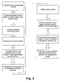
- FIG. 3 DETAILED ELECTRODE FABRICATION METHOD USING DIRECT PHOTOLITHOGRAPHY: This figure shows method steps corresponding to FIG. 2 .
- FIG. 4 DEVICE STRUCTURE: This figure illustrates a ) sectional view of a CZT device with single layer electrodes and b ) perspective view of the tile and c ) and d ) are an expanded view of a pixel electrode section showing additional contact layers for PCB assembly.
- FIG. 5 ELECTRICAL CHARACTERISTICS OF CZT DEVICE USING ELECTRODE FABRICATION METHODS: This figure shows in a ) an I-V curve showing the blocking nature of the metal contact, and in b ) a resistivity curve for the CZT device.
- FIG. 6 RADIATION DETECTOR SPECTRAL PERFORMANCE: This figure shows experimental data for the energy resolution response of an 8 ⁇ 8 pixel detector device fabricated by the embodied methods.
- FIG. 7 is a schematic plan view of on contact configuration on a detector substrate.
- FIG. 8 is a schematic plan view of another contact configuration on a detector substrate.
- FIG. 9 is a schematic plan view of a further contact configuration on a detector substrate.
- FIG. 10 is a schematic plan view of a further contact configuration of a coplanar grid design with two interlocking anode patterns on a detector substrate.
- FIG. 11 a ) is a perspective view of a further contact configuration of a strip detector with orthogonal coplanar anode strips on a detector substrate and b ) is a top view of one unit cell.
- FIG. 12 a ) is a side view and b ) is a top view of a further contact configuration with coplanar anode strips on a detector substrate and a unitary cathode.
- FIG. 13 is a perspective view of a further contact configuration of a strip detector with coplanar anode strips and orthogonal cathode strips on a detector substrate.
- FIG. 14 a ) is a perspective view of a further contact configuration of a strip detector with an additional interpixel grid and b ) is a top view of one cell.
- the present invention embodiments provide a method for fabricating pixilated imaging detectors via a direct lithography technique, resulting in a high value of interpixel resistivity and durable adhesion, substantially no oxide layer (i.e., completely no oxide layer or having an unavoidable trace amount of oxide, but not discrete oxide layer) and providing a blocking contact.
- the planar electrode When used for radiation detection, the planar electrode will be positioned facing the radiation source. The planar electrode will be referred to as being on the front device surface, and the pixel array electrodes as being on the rear device surface.
- the process disclosed herein comprises depositing contact electrode layers on at least the rear surfaces of the CZT tile, then forming pixel electrodes on the rear detector surface by applying a resist on at least said rear detector surface contact layer and exposing resist covering selected interpixel regions using a direct photolithography mask covering, then etching said exposed interpixel resist regions with an etchant to remove substantially all deposited contact material in the interpixel gap regions, and finally stripping the remaining resist.
- the direct lithography process provides an optimized metal/semiconductor contact such that it not only provides excellent adhesion but also precludes oxidation at the metal/semiconductor interface as well as providing a semi-blocking contact that prevents charge injection.
- the metal removal method provides a stable and high resistance interpixel region such that the interpixel leakage current is minimized.
- the forming process ensures reliability during assembly and use as a radiation detector, especially printed circuit board (PCB) attachment such as by the low temperature soldering technique.
- PCB printed circuit board
- segmented contacts made by the direct lithography process are strongly adhered to the CZT crystal, sufficient to remain adhered when stressed by contacting a region of the electrode surface with Scotch brand adhesive tape then applying sufficient force to peel and remove the tape from the contacted electrode region.
- CdZnTe (CZT) crystals are useful for fabrication of small, portable, room temperature radiation detectors.
- the method for fabricating segmented detectors via direct photolithography reduces interpixel surface leakage current, increases interpixel resistance and provides durable adhesion of the metal electrode on the surface of the CZT crystal. Improved energy resolution is the result.
- a four step process is disclosed, wherein metal is deposited on CZT, a resist is applied and the resist is developed by a direct lithography technique, and interpixel regions are etched to remove metal from the CZT surface, and the remaining resist is removed. While direct photolithography is preferred, other direct lithography methods, such as direct nanoimprint lithography in which the masking layer is indented instead of exposed to radiation, may be used.
- the invention finds particular, but not exclusive use, with substrates formed of cadmium telluride (CdTe) or cadmium zinc telluride (CdZnTe).
- the substrate is preferably a sliced and polished single crystal (such as CZT) wafer material. When the substrate is in a rectangular form with major front and rear surfaces, it is referred to also as “tile.” It will be appreciated that the method of the invention can be used with other substrate materials as well.
- contact or contact material refers to a conductive coating, selected from the group including metals, semiconductors or hybrid conductors (such as silicides).
- the conductive contact layer is a metal or metal alloy.
- the metal layer for forming the contacts is applied by a method such as physical deposition (sputtering, evaporation) or chemical deposition methods (electrolytic).
- the metal layer for forming the contacts comprises gold (Au), although other metals, for example platinum (Pt) or indium (In), could also be used.
- Electrode arrays There are many configurations of electrode arrays and many applications to which the invention may be applied.
- CZT is used as the bulk crystal material in the examples
- Au is used in the specific recipes and experimental results with additional multi-layers as described, but the method is not limited to gold contacts.
- interpixel surface leakage has an intrinsic surface leakage component from the monolithic CZT, which is low in high quality CZT, and additional surface leakage from the fabrication process of depositing and removing the contact layer in the interpixel region.
- the fabrication techniques have a critical effect on interpixel resistance and contact “adhesion”, and must be optimized and balanced.
- the methods embodied herein are reliable, low cost methods of fabricating high performance imaging-grade large area pixilated CZT detectors using a direct photolithography fabrication technique.
- this method is well-suited for multi-layer contacts and for a range of deposition processes, including physical deposition and electroless deposition.
- CZT detectors using CZT bulk crystal made by the high quality THM crystal growth process and fabricated by the invented method, have shown new and unmatched high resistivity performance.
- the techniques can be successfully applied to crystals formed by all other crystal growth processes, resulting in relative improvement over traditional detector fabrication. Excellent contact adhesion is observed due to the avoidance of contamination during direct deposition, improved photolithography and appropriate annealing.
- the fabrication method and the resulting fabricated detector array with characteristics resulting from the fabrication are believed to be novel.
- Additional configurations of a fabricated radiation detector can be applied at various stages using the process. For example, a basic process would just pixelate the anode side of the crystal substrate with a single contact layer. The opposing side could be optionally fabricated simultaneously or before or after as an additional stage.
- the preferred configuration uses multiple contact layers for improved contact use in assembly of the radiation detector as explained later.
- multi-layers there are again several process options. Firstly, the multiple layers can be integrated into the direct photolithography process or, alternatively, the additional contact layers can be added after the direct photolithography process, providing flexibility on the positioning and size of the additional layers. Additional processes desired for final configuration and packaging are also described for the resulting detector devices.
- a basic single layer fabrication process is shown in FIG. 1 , having a deposition step, then a direct photolithography treatment followed by etching the contact material in the interpixel gaps, and finally, resist stripping.
- Optional steps of side polishing and sealing the sides are included.
- the method starts in step 100 with applying contact electrode layers by deposition on at least the rear surface of the CZT tile. Preferably all surfaces of the tile are coated. This can be done either by physical deposition or chemical methods such as sputtering or electroless deposition. In this broadest application of the technique there is only a single contact layer.
- the deposited contact provides a blocking contact that prevents charge injection and hence leads to lower leakage current, and the deposition has no oxide layer between contact and CZT.
- step 101 pixel electrodes are formed on the rear detector surface by applying a resist on at least the rear detector surface contact layer.
- Step 102 a direct mask is aligned to the resist and used to selectively expose the interpixel regions to a UV source.
- the exposed resist is developed at this step, as will be described further on.
- the contact material in the interpixel gaps is removed by etching in step 103 .
- the exposed interpixel resist regions are etched with a bromine-based etchant and process to remove substantially all deposited gold contact in the interpixel gap regions.
- step 104 the remaining resist is stripped from the remaining masked electrode regions on the front planar electrode surface and rear pixilated electrode surfaces.
- any remaining contact material on., the tile sides can be removed, typically by polishing, and a common protective coating added.
- the combined effect of the method is a high performance radiation detector device as is demonstrated herein.
- FIG. 2 illustrates an example of a detailed method in accordance with the invention, of forming tri-layer metal contacts on a semiconductor substrate at positions (pixels) for defining radiation detector cells with an interpixel gap with high resistivity between the detector cells.
- the semiconductor substrate is made of cadmium zinc telluride (CdZnTe) or cadmium telluride (CdTe), although it will be appreciated that other semiconductor materials, for example lead iodide, thallium bromide, gallium arsenide or silicon, can be used.
- the metal used for the metallization layer and the contacts is gold, although it will be appreciated that other metals, alloys or other conductive materials, for example platinum or indium, could be used.
- FIG. 2 is a schematic cross-sectional view from the side of a detector substrate at various stages in the formation of gold contacts on a CdZnTe substrate.
- the detailed features and structure at each step of the process are shown, resulting in an array of contact pixels on the rear surface of the CZT (drawn as facing up in this illustration), protective side coatings, and a single electrode on the front surface of the CZT tile (drawn as facing down in this illustration).
- two additional contact layers are added on to the pixilated primary contact layer on the rear side, for improved device assembly.
- the steps of the process are detailed in FIG. 3 .
- the process can be applied to any array size and pixel configuration for CZT devices.
- a typical device size is a 20 ⁇ 20 ⁇ 5 mm detector, having 8 ⁇ 8 pixels or 11 ⁇ 11 pixels depending on the application.
- the CZT wafer is polished and etched such that high quality clean crystal surfaces are prepared for the deposition process.
- the direct lithography fabrication process is described with reference to both FIGS. 2 and 3 , and for the case of the primary contact being gold, with two additional contact layers and for simultaneous forming of the cathode contact on the opposing side of the CZT tile.
- a primary layer of gold 200 is deposited on the CZT tile 304 .
- the devices described used electroless deposition, but alternatively the gold may be deposited by known techniques, such as sputtering.
- the CZT tiles are first cleaned in acetone, as is well known.
- the clean CZT tiles 304 are dipped in an electroless gold solution for several minutes depositing a gold layer 200 , then the tile is removed and rinsed with methanol. Typical thickness of deposition is equal or more than 100 nm.
- the deposited gold may be annealed at 90 deg C. for 15 minutes to increase adhesion to the substrate. An adhesion test can be done after a few hours using Scotch tape to confirm quality of the adhesion.
- step 2 two additional contact layers are deposited onto the rear (side to be pixilated) side of the tile, over the primary contact on the rear side.
- a Ni layer 312 is deposited using sputtering or a thermal evaporation process to a thickness ⁇ 100 nm and nominally 50 nm.
- gold layer 310 is deposited using sputtering, thermal evaporation and/or an electroless process to a thickness ⁇ 50 nm and nominally 20 nm.
- Alternative conductive contact material can be substituted for either or both of the additional contact layers.
- a photoresist 202 is applied over the contact layer(s).
- Tiles 304 are dipped in resist, for example Shipley 1805 resist. Excessive resist is removed if necessary from the edge using a Q-tip, making sure the resist does not form any edge bead (especially on the pixilated face) as this would be detrimental for the pixel quality. Generally, the least possible amount of resist should remain on the pixilated face. The resist should be dried out for 10 minutes with the pixilated face kept up and horizontal.
- the resist coating is hardened in step 4 by baking for 10 minutes at 90° C. This step is done to drive excess solvent out of the resist.
- the tile is now prepared for lithography exposure.
- a pixel pattern is formed on the rear side of the tile 304 by photolithography.
- a UV mask 204 is aligned over the CZT tile surface, and the negative resist is exposed to UV.
- the direct lithography mask shades regions of the resist in a selected pixel pattern and exposes interpixel gaps to UV radiation.
- a contact mask is used but other methods will work as well, such as proximity and projection masks.
- a glass plate is placed on top making sure that the glass plate is horizontal. This ensures uniform contact between the tile and the mask. For the example resist, exposure by a UV lamp (254 nm wavelength) for several minutes is suitable. If desired, a positive resist may be used instead of the negative resist (in which case, the exposure mask's transparent and opaque regions are reversed).
- step 6 the exposed photoresist is developed.
- the resist developer for example Microposit developer, MF-319
- the tiles are placed into the developer with the pixilated side facing up, developed for 2 minutes and the tile(s) are removed from the developer and rinsed in de-ionized water.
- the UV exposed resist is removed, in preparation for creating the interpixel gap.
- step 7 the remaining resist (pixel pattern) is baked for 20 minutes at 90° C. This step is done to harden the resist further.
- the exposed contact regions 316 are etched.
- the following etching solution is suitable for etching through either just the primary contact layer or the optional three-layer contact.
- a 2% Br-Ethanol Glycol (BrEG) solution is prepared by pouring a 25 ml of Ethylene Glycol into a plastic beaker, then 0.5 ml of Bromine is added using a disposable pipette. Using the same pipette, the solution is mixed thoroughly until it becomes uniform. However, a different pipette or mixing device may also be used. Etching is conducted for approximately 3 minutes. This etching is done to remove unmasked interpixel contact material.
- Disposable pipettes can be used to create Br-EG constant flow to agitate for better etching.
- a different pipette or agitation or mixing device may also be used.
- the spray etching technique should rapidly remove contact material flakes from the interpixel gaps, resulting in high interpixel resistance.
- the tiles are removed from the etchant and rinsed in deionized water.
- the remaining resist is stripped using an acetone bath, resulting in tile 320 with a pixel array of contacts. No photoresist therefore remains on the CdTe/CdZnTe detector since it is usually a hydroscopic material that in time would absorb humidity and deteriorate the detector performance.
- step 10 the primary contact material (in this example gold) on the sides of the fabricated CZT device 322 is removed by side polishing.
- the side of the tile(s) are first polished with 1200 grit then with 0.3 micron as fine polish.
- An alternate embodiment could, in step 1, mask the sides of the CZT tile instead of depositing gold on all sides. For this reason, the side contact removal step 10 may be optional.
- the resulting fabricated CZT device has a cathode contact 200 remaining on the front side, a pixilated anode contact array formed of a primary contact 200 , and secondary contact layers 312 and 310 , separated by interpixel gap 316 .
- FIG. 2 illustrates the multi-layer pixels as being identical width in cross-section for illustrative purpose.
- the preferred embodiment is that the secondary contact layers are smaller in area than the primary contact pixel, as shown in FIG. 4 . This can be realized by applying the secondary contacts via sputtering.
- a protective coating is applied to the polished side edges shown as coating 308 FIG. 4 a .
- the CZT tile is dipped in a protective coating (such as Humiseal) to cover the exposed sides and dried for at least 5 hours.
- FIG. 4 a - c The structure of the fabricated CZT detector devices 300 , are shown in FIG. 4 a - c .
- monolithic CZT crystal 304 has a planar contact electrode 306 on a front side and an array of pixel contact electrodes 302 on a rear side separated by interpixel gaps 316 .
- the side edges have no electrode layer, and the CZT surface is polished and sealed by coating 308 .
- a cutaway is shown in perspective view in FIG. 4 b showing an array of pixels suitable for radiation detection.
- each anode electrode in FIGS. 4 c and 4 d comprises a gold contact layer 302 contacting the substrate, a nickel layer 312 having a thickness of at least 50 nm and another gold layer 310 having a thickness of at most 50 nm.
- the trilayer electrode may be formed by forming another photoresist pattern on a surface of said pixilated anode electrode array with openings to said array surface that are equal or less than an area of each pixel anode electrode 302 , depositing the second conductive layer 312 and the third conductive layer 310 over the photoresist pattern, and removing the photoresist pattern to lift off portions of the second and third conductive layers to form an array of trilayer pixel anode electrodes in which the first conductive layer portion 302 is wider than the second 312 and third 310 conductive layer portions in each pixel.
- FIG. 5 shows the electrical characteristics of CZT detector devices having electrodes fabricated by the taught embodiments.
- the I-V curve in FIG. 5 a demonstrates the blocking nature of the deposited gold metal contact, as well as low total device leakage current.
- the device resistivities are derived from the I-V curve and shown in FIG. 5 b . It can be seen that device resistivity measured at 100V bias is greater than 5 ⁇ 10 10 ⁇ -cm, such as greater than about 10 11 ⁇ -cm, and bulk resistivity at the ⁇ 1V region remains high also.
- CZT detector devices 300 resulted in improved devices, faster fabrication methods and lower cost fabrication methods. For example, interpixel resistance improved from less than or equal to 10 8 Ohm to greater than 2 ⁇ 10 9 ohm, due to the contact structures fabricated by the methods described herein. Additionally the fabrication method leads to improved yield of responsive pixels within the CZT detector device 300 . All 64 pixels of an 8 ⁇ 8 array produced ER signals using the traveling heater method (THM) grown CZT bulk crystal under standard radiation testing. FIG. 6 shows the energy resolution results demonstrating that all 64 pixels provide excellent signal, and all have FWHM ⁇ 5.5%, such as 3.7 to 5.4% for each pixel.
- THM traveling heater method
- the resulting device demonstrated device resistivity greater than about 10 11 ⁇ -cm, interpixel resistance greater than 2 ⁇ 10 9 Ohm, which is believed to be significantly better than the prior art values.
- the adhesion properties of the gold electrodes to the CZT are exceptional, and pass the Scotch tape (3M brand) adhesion test per standard ASTM testing methodology with 100% yields (Test Reference: with respect to the ASTM D3330/D3330M-04 Standard test method for peel adhesion of pressure-sensitive tape: Under Test Method A standard conditions the particular tape used to test the adhesion (3M—BP2018) gives a result of 22 oz. on a 1.0′′ wide front per 3M Company Inc).
- FIGS. 7 , 8 and 9 are used to illustrate possible pixel contact patterns on the upper surface of the detector substrate.
- an array of square pixel contact pads is shown, as is commonly used.
- an array of circular pixel pads is shown.
- the use of circular rather than square pixel pads increases the surface resistance between pads by increasing the amount of resistive material between adjacent pads.
- FIG. 9 illustrates an array of offset honeycombed pixel pads. Once again this further increases the resistance between pads by increasing the surface amount of resistive material between adjacent pads.
- These patterns are included as possible examples. Devices fabricated by the method do not require additional resistive material or gap, which would reduce spatial resolution of the detector.
- FIG. 10 An alternate contact configuration is shown in FIG. 10 of a coplanar grid design with two interlocking anode patterns on a detector substrate.
- Coplanar anode 410 is interspersed between the fingers of coplanar anode 412 . Both are surrounded by boundary electrode 414 .
- the spacing between anode fingers is the effective interpixel gap.
- the detector configuration may be fabricated by the direct photolithography process.
- FIG. 11 A strip detector with orthogonal coplanar anode strips on a detector substrate is shown in FIG. 11 .
- Each anode cell 420 has a collecting pixel 422 and non-collecting portion 424 , which are connected in orthogonal directions as shown.
- the effective interpixel region is the gap surrounding the collecting pixel.
- the dimensions are for illustration, as will be appreciated by one skilled in the art, a wide range of dimensions can be applied to the same configuration.
- a detector type as shown in FIG. 11 can be fabricated by the direct photolithography process.
- a coplanar grid detector 430 is shown in side and top views in FIGS. 12 a and 12 b with coplanar anode strips ( 432 , 434 in the top view) on a detector substrate and a unitary cathode 436 .
- the effective “interpixel gap” is the region 438 separating adjacent anode strips.
- a detector type as shown in FIG. 12 can be fabricated by the direct photolithography process.
- FIG. 13 Another strip detector 440 is shown in FIG. 13 having coplanar anode strips 442 and orthogonal cathode strips 444 on a detector substrate.
- the effective “interpixel gap” is the region 438 separating adjacent anode strips.
- the dimensions and electronics are for illustration and are not limiting to the example, as will be appreciated by one skilled in the art. A wide range of dimensions can be applied to the same configuration.
- the detector type as shown in FIG. 13 can be fabricated by the direct photolithography process.
- FIGS. 14 a and 14 b A cross-strip radiation-detector 1200 is shown in FIGS. 14 a and 14 b , as referenced from U.S. Pat. No. 6,037,595.
- An expanded cell in FIG. 14 b shows the detailed electrode construction of each detection element.
- a first surface of a slab of semiconductor crystal 1210 has a continuous layer of conducting material to form a bias electrode 1220 . If the mobility-lifetime product of the electrons is larger than that of the holes for the semiconductor 1210 , the bias electrode 1220 is the cathode.
- an array of anode detection elements is formed on the second surface opposing the first surface.
- the anode array includes typically three sets of electrodes: a control electrode grid 1230 , a plurality of small “dot”-like anode electrodes 1232 , and shield electrodes 1234 .
- the control electrode grid 1230 is preferably formed by two mutually orthogonal and intersecting sets of thin parallel conducting lines plated on the surface of the semiconductor 1210 to form open anode areas around anodes 1232 .
- a small anode 1232 is formed on the surface of the semiconductor (e.g., by plating).
- the shield electrode 1234 substantially fills the open anode area but with a small gap 1235 to provide electrical insulation to the control grid 1230 .
- the shield electrode 1234 has a center opening which generally surrounds the anode 1232 .
- the opening 1236 is as small as possible but still large enough to provide a gap 1238 which insulates the anode 1232 from the shield electrode 1234 .
- the gaps 1235 and 1238 may be filled with a dielectric material to improve the electrical insulation.
- the dimensions and electronics are for illustration and are not limiting to the example, as will be appreciated by one skilled in the art. A wide range of dimensions can be applied to the same configuration.
- the detector type of FIG. 14 can be fabricated by the direct photolithography process.
- various shaping/shielding ring configurations as are common in the CZT detector industry can be used with the device to further enhance performance. It is possible to apply the resist only to the rear surface of the wafer 304 where the pixels will be formed by an additional step of applying protective coating to the remainder of the CZT tile 304 prior to gold plating and resist application. This method could apply when the opposing planar electrode deposition is done separately such as by another deposition process.
- the method can be also used for fabrication of an integrated shielding cathode, with a configuration as described in co-pending patent applications “Segmented radiation detector with side shielding cathode” (U.S. application Ser. No. 11/527,707 filed Sep. 27, 2006 and Canadian application number 2,541,256, filed on Feb. 22, 2006).
- Gold is an advantageous material because it can be readily etched to define the desired contact structures and give good contact (better than aluminum, for example) to the CdZnTe.
- conductive material or metal contacts e.g. platinum, nickel, aluminum, nickel/gold alloy, platinum/gold alloy, titanium/tungsten or cadmium sulfide
- a radiation imaging device can be constructed by connecting a radiation detector produced by the method according to one of the above described methods to a readout chip having circuits for accumulating charge from successive radiation hits, individual contacts (e.g. pixel pads) for respective detector cells being ‘flip-chip’ joined (e.g., by bump bonding using balls of indium or conductive polymer material, gluing using one-way conductive materials, or other conductive adhesive layer techniques) to respective circuits for accumulating charge.
- the invention teaches how to obtain a radiation detector (e.g. based on a CdZnTe substrate) with one side metallized according to a desired pattern with maximum possible electrical resistivity separation between the metal contacts.
- a radiation detector e.g. based on a CdZnTe substrate
- High resistivity between metal contacts is desirable to improve contrast resolution and eliminate signal leakage between adjacent metal contacts on the substrate surface.
Abstract
Description
-
- a. Good adhesion.
- b. Capable of preventing charge injection.
- c. Capable of preventing the inclusion of “oxides” beneath the metal—an intermediate oxide layer sandwiched in between the metal and the CZT will lower the barrier height and potentially cause polarization, having a negative effect on detector performance.
- d. Reliable for assembly processes, including low temperature soldering.
Claims (29)
Priority Applications (5)
| Application Number | Priority Date | Filing Date | Title |
|---|---|---|---|
| US11/633,091 US7728304B2 (en) | 2006-02-22 | 2006-12-04 | Method of making segmented contacts for radiation detectors using direct photolithography |
| JP2008556380A JP2009527922A (en) | 2006-02-22 | 2007-02-21 | Method for manufacturing segmented contacts for radiation detectors using direct photolithography |
| EP07751102.0A EP1996961A4 (en) | 2006-02-22 | 2007-02-21 | Method of making segmented contacts for radiation detectors using direct photolithography |
| PCT/US2007/004319 WO2007100538A2 (en) | 2006-02-22 | 2007-02-21 | Method of making segmented contacts for radiation detectors using direct photolithography |
| IL193577A IL193577A0 (en) | 2006-02-22 | 2008-08-20 | Method of making segmented contacts for radiation detectors using direct photolitography |
Applications Claiming Priority (5)
| Application Number | Priority Date | Filing Date | Title |
|---|---|---|---|
| CA2541256 | 2006-02-22 | ||
| CA2,541,256 | 2006-02-22 | ||
| CA 2541256 CA2541256A1 (en) | 2006-02-22 | 2006-02-22 | Shielding electrode for monolithic radiation detector |
| US11/527,707 US7223982B1 (en) | 2006-02-22 | 2006-09-27 | Segmented radiation detector with side shielding cathode |
| US11/633,091 US7728304B2 (en) | 2006-02-22 | 2006-12-04 | Method of making segmented contacts for radiation detectors using direct photolithography |
Related Parent Applications (1)
| Application Number | Title | Priority Date | Filing Date |
|---|---|---|---|
| US11/527,707 Continuation-In-Part US7223982B1 (en) | 2006-02-22 | 2006-09-27 | Segmented radiation detector with side shielding cathode |
Publications (2)
| Publication Number | Publication Date |
|---|---|
| US20070194243A1 US20070194243A1 (en) | 2007-08-23 |
| US7728304B2 true US7728304B2 (en) | 2010-06-01 |
Family
ID=38056756
Family Applications (2)
| Application Number | Title | Priority Date | Filing Date |
|---|---|---|---|
| US11/527,707 Active US7223982B1 (en) | 2006-02-22 | 2006-09-27 | Segmented radiation detector with side shielding cathode |
| US11/633,091 Active 2028-01-14 US7728304B2 (en) | 2006-02-22 | 2006-12-04 | Method of making segmented contacts for radiation detectors using direct photolithography |
Family Applications Before (1)
| Application Number | Title | Priority Date | Filing Date |
|---|---|---|---|
| US11/527,707 Active US7223982B1 (en) | 2006-02-22 | 2006-09-27 | Segmented radiation detector with side shielding cathode |
Country Status (6)
| Country | Link |
|---|---|
| US (2) | US7223982B1 (en) |
| EP (2) | EP1989572A4 (en) |
| JP (1) | JP2009527922A (en) |
| CA (1) | CA2541256A1 (en) |
| IL (1) | IL193577A0 (en) |
| WO (1) | WO2007097782A1 (en) |
Cited By (7)
| Publication number | Priority date | Publication date | Assignee | Title |
|---|---|---|---|---|
| US20090218647A1 (en) * | 2008-01-23 | 2009-09-03 | Ev Products, Inc. | Semiconductor Radiation Detector With Thin Film Platinum Alloyed Electrode |
| US20090250692A1 (en) * | 2008-04-07 | 2009-10-08 | Ev Products, Inc. | Radiation Detector With Asymmetric Contacts |
| US20090311860A1 (en) * | 2008-06-12 | 2009-12-17 | Usa As Represented By The Administrator Of The National Aeronautics And Space Administration | Blocking contacts for n-type cadmium zinc telluride |
| US20100252744A1 (en) * | 2009-04-06 | 2010-10-07 | Koninklijke Philips Electronics N.V. | Radiation detector with a plurality of electrode systems |
| US20110272589A1 (en) * | 2010-05-03 | 2011-11-10 | Brookhaven Science Associates, Llc | Hybrid Anode for Semiconductor Radiation Detectors |
| US8742522B2 (en) | 2012-04-10 | 2014-06-03 | Ev Products, Inc. | Method of making a semiconductor radiation detector |
| US20140355745A1 (en) * | 2012-01-27 | 2014-12-04 | Hitachi, Ltd | Semiconductor radiation detector and nuclear medicine diagnosis device |
Families Citing this family (33)
| Publication number | Priority date | Publication date | Assignee | Title |
|---|---|---|---|---|
| US20110034769A1 (en) * | 1997-10-06 | 2011-02-10 | Micro-Imaging Solutions Llc | Reduced area imaging device incorporated within wireless endoscopic devices |
| US7462833B2 (en) * | 2007-04-17 | 2008-12-09 | Redlen Technologies | Multi-functional cathode packaging design for solid-state radiation detectors |
| US8847386B2 (en) * | 2007-06-29 | 2014-09-30 | Koninklijke Philips N.V. | Electrical contact for a cadmium tellurium component |
| US7636638B2 (en) * | 2007-11-27 | 2009-12-22 | Canberra Industries, Inc. | Hybrid radiation detection system |
| US7955992B2 (en) * | 2008-08-08 | 2011-06-07 | Redlen Technologies, Inc. | Method of passivating and encapsulating CdTe and CZT segmented detectors |
| US8614423B2 (en) * | 2009-02-02 | 2013-12-24 | Redlen Technologies, Inc. | Solid-state radiation detector with improved sensitivity |
| US9202961B2 (en) | 2009-02-02 | 2015-12-01 | Redlen Technologies | Imaging devices with solid-state radiation detector with improved sensitivity |
| US8314395B2 (en) * | 2009-08-31 | 2012-11-20 | General Electric Company | Semiconductor crystal based radiation detector and method of producing the same |
| US8476101B2 (en) * | 2009-12-28 | 2013-07-02 | Redlen Technologies | Method of fabricating patterned CZT and CdTe devices |
| US8296940B2 (en) | 2010-04-19 | 2012-10-30 | General Electric Company | Method of forming a micro pin hybrid interconnect array |
| US9134439B2 (en) * | 2010-05-03 | 2015-09-15 | Brookhaven Science Associates, Llc | Array of virtual Frisch-grid detectors with common cathode and reduced length of shielding electrodes |
| US9121953B2 (en) * | 2010-05-03 | 2015-09-01 | Brookhaven Science Associates, Llc | Array of virtual Frisch-grid detectors with common cathode and reduced length of shielding electrodes |
| WO2012118898A2 (en) * | 2011-03-01 | 2012-09-07 | The Government Of The United States Of America, As Represented By The Secretary Of The Navy | Isolating segmented radiation detectors using alumina |
| WO2013006453A1 (en) * | 2011-07-01 | 2013-01-10 | Brookhaven Science Associates, Llc | Radiation detector device for rejecting and excluding incomplete charge collection events |
| CN103094405A (en) * | 2011-11-04 | 2013-05-08 | 中国原子能科学研究院 | Preparation process of CdZnTe detector of capacitive Frisch grid |
| US9000389B2 (en) * | 2011-11-22 | 2015-04-07 | General Electric Company | Radiation detectors and methods of fabricating radiation detectors |
| US8884228B2 (en) | 2012-01-27 | 2014-11-11 | Savannah River Nuclear Solutions, Llc | Modification of solid state CdZnTe (CZT) radiation detectors with high sensitivity or high resolution operation |
| CN103972323B (en) * | 2013-01-31 | 2017-05-03 | 同方威视技术股份有限公司 | Radiation detector |
| DE102013202630B4 (en) * | 2013-02-19 | 2017-07-06 | Siemens Healthcare Gmbh | Radiation detector and medical diagnostic system |
| WO2015063665A1 (en) | 2013-11-01 | 2015-05-07 | Koninklijke Philips N.V. | Radiation detector and detection method having reduced polarization |
| DE102014211602B4 (en) * | 2014-06-17 | 2018-10-25 | Siemens Healthcare Gmbh | Detector module for an X-ray detector |
| JP6316960B2 (en) * | 2014-07-03 | 2018-04-25 | Jx金属株式会社 | UBM electrode structure for radiation detector, radiation detector and manufacturing method thereof |
| EP3161522B1 (en) * | 2014-12-05 | 2018-02-28 | Koninklijke Philips N.V. | X-ray detector device for inclined angle x-ray radiation |
| CN106249269B (en) * | 2016-08-31 | 2023-05-23 | 同方威视技术股份有限公司 | Semiconductor detector |
| JP2020521318A (en) * | 2017-05-09 | 2020-07-16 | ケーエー・イメージング・インコーポレイテッド | Device for radiation detection in a digital imaging system |
| CN110914715B (en) * | 2017-07-26 | 2023-09-22 | 深圳帧观德芯科技有限公司 | Radiation detector and method for manufacturing the same |
| WO2019019041A1 (en) * | 2017-07-26 | 2019-01-31 | Shenzhen Xpectvision Technology Co., Ltd. | Methods of making and using an x-ray detector |
| TWI683428B (en) | 2018-03-29 | 2020-01-21 | 日商Jx金屬股份有限公司 | Radiation detection element and its manufacturing method |
| US10813607B2 (en) * | 2018-06-27 | 2020-10-27 | Prismatic Sensors Ab | X-ray sensor, method for constructing an x-ray sensor and an x-ray imaging system comprising such an x-ray sensor |
| CN109669204B (en) | 2019-01-08 | 2019-09-06 | 山西医科大学 | A kind of CZT semiconductor activity meter and activity measurement device |
| CN112436062B (en) * | 2020-12-01 | 2022-12-02 | 上海大学 | Composite electrode for tellurium-zinc-cadmium radiation detector and preparation method thereof |
| US11688821B2 (en) * | 2021-07-26 | 2023-06-27 | Henry Meyer Daghighian | Wireless gamma and/or hard x-ray radiation detector |
| CN115295638A (en) * | 2022-08-29 | 2022-11-04 | 通威太阳能(成都)有限公司 | Solar cell and preparation process thereof |
Citations (32)
| Publication number | Priority date | Publication date | Assignee | Title |
|---|---|---|---|---|
| US4144090A (en) | 1977-10-25 | 1979-03-13 | Ppg Industries, Inc. | Non-oxidative removal of gold films |
| JPH02129969A (en) * | 1988-11-09 | 1990-05-18 | Shimadzu Corp | Radiation detecting semiconductor element array |
| US5677539A (en) | 1995-10-13 | 1997-10-14 | Digirad | Semiconductor radiation detector with enhanced charge collection |
| US5905264A (en) | 1996-08-14 | 1999-05-18 | Imarad Imaging Systems Ltd. | Semiconductor detector |
| US5933706A (en) | 1997-05-28 | 1999-08-03 | James; Ralph | Method for surface treatment of a cadmium zinc telluride crystal |
| US6034373A (en) | 1997-12-11 | 2000-03-07 | Imrad Imaging Systems Ltd. | Semiconductor radiation detector with reduced surface effects |
| US6037595A (en) | 1995-10-13 | 2000-03-14 | Digirad Corporation | Radiation detector with shielding electrode |
| US6043106A (en) | 1997-05-28 | 2000-03-28 | Mescher; Mark J. | Method for surface passivation and protection of cadmium zinc telluride crystals |
| US6046068A (en) | 1995-11-29 | 2000-04-04 | Simage Oy | Forming contacts on semiconductor substrates radiation detectors and imaging devices |
| US6069360A (en) | 1998-05-08 | 2000-05-30 | Lund; James C. | Method and apparatus for electron-only radiation detectors from semiconductor materials |
| US6175120B1 (en) | 1998-05-08 | 2001-01-16 | The Regents Of The University Of Michigan | High-resolution ionization detector and array of such detectors |
| US6212093B1 (en) | 2000-01-14 | 2001-04-03 | North Carolina State University | High-density non-volatile memory devices incorporating sandwich coordination compounds |
| US20010035497A1 (en) | 2000-04-27 | 2001-11-01 | Guillaume Montemont | Detector support device for detecting ionizing radiations |
| US6333504B1 (en) | 1995-10-13 | 2001-12-25 | Digirad Corp | Semiconductor radiation detector with enhanced charge collection |
| US6362484B1 (en) * | 1995-07-14 | 2002-03-26 | Imec Vzw | Imager or particle or radiation detector and method of manufacturing the same |
| US20020066531A1 (en) | 1996-11-29 | 2002-06-06 | Applied Materials, Inc. | Shield or ring surrounding semiconductor workpiece in plasma chamber |
| US6410922B1 (en) | 1995-11-29 | 2002-06-25 | Konstantinos Evangelos Spartiotis | Forming contacts on semiconductor substrates for radiation detectors and imaging devices |
| US6465860B2 (en) * | 1998-09-01 | 2002-10-15 | Kabushiki Kaisha Toshiba | Multi-wavelength semiconductor image sensor and method of manufacturing the same |
| US20020158207A1 (en) | 1996-11-26 | 2002-10-31 | Simage, Oy. | Forming contacts on semiconductor substrates for radiation detectors and imaging devices |
| US20020182716A1 (en) | 2000-08-21 | 2002-12-05 | Claude Weisbuch | Support for chromophoric elements |
| US6524966B1 (en) | 1997-05-28 | 2003-02-25 | Sandia National Laboratories | Surface treatment and protection method for cadmium zinc telluride crystals |
| US20030173523A1 (en) * | 2002-03-13 | 2003-09-18 | Vuorela Mikko Ilmari | Low temperature, bump-bonded radiation imaging device |
| US20040052456A1 (en) | 2000-05-26 | 2004-03-18 | Pierpaolo Boffi | Cdznte eletro-optical switch |
| US6765213B2 (en) | 2000-07-30 | 2004-07-20 | Imarad Imaging Systems Ltd. | Gamma-ray detector for coincidence detection |
| US6781132B2 (en) | 2001-08-10 | 2004-08-24 | The Regents Of The University Of Michigan | Collimated radiation detector assembly, array of collimated radiation detectors and collimated radiation detector module |
| US20050167606A1 (en) | 2003-08-20 | 2005-08-04 | Harrison Fiona A. | Cadmium-zinc-telluride detectors |
| US20050189474A1 (en) * | 2004-02-20 | 2005-09-01 | Taizo Tomioka | Semiconductor relay apparatus and wiring board fabrication method |
| US20050230627A1 (en) * | 2002-04-18 | 2005-10-20 | Forschungszentrum Julich Gmbh | Position-sensitive germanium detectors having a microstructure on both contact surfaces |
| US7038288B2 (en) | 2002-09-25 | 2006-05-02 | Microsemi Corporation | Front side illuminated photodiode with backside bump |
| US20060255280A1 (en) * | 2003-03-10 | 2006-11-16 | Hamamatsu Photonics K.K. | Photodiode array, method for manufacturing same, and radiation detector |
| US20080042070A1 (en) * | 2004-09-30 | 2008-02-21 | Levin Craig S | Semiconductor Crystal High Resolution Imager |
| US7576369B2 (en) * | 2005-10-25 | 2009-08-18 | Udt Sensors, Inc. | Deep diffused thin photodiodes |
Family Cites Families (3)
| Publication number | Priority date | Publication date | Assignee | Title |
|---|---|---|---|---|
| US6649915B2 (en) * | 1998-07-16 | 2003-11-18 | Sandia National Laboratories | Ionizing radiation detector |
| US6838741B2 (en) * | 2002-12-10 | 2005-01-04 | General Electtric Company | Avalanche photodiode for use in harsh environments |
| US7589324B2 (en) * | 2006-12-21 | 2009-09-15 | Redlen Technologies | Use of solder mask as a protective coating for radiation detector |
-
2006
- 2006-02-22 CA CA 2541256 patent/CA2541256A1/en not_active Abandoned
- 2006-09-27 WO PCT/US2006/037458 patent/WO2007097782A1/en active Application Filing
- 2006-09-27 EP EP06804162.3A patent/EP1989572A4/en not_active Withdrawn
- 2006-09-27 US US11/527,707 patent/US7223982B1/en active Active
- 2006-12-04 US US11/633,091 patent/US7728304B2/en active Active
-
2007
- 2007-02-21 JP JP2008556380A patent/JP2009527922A/en active Pending
- 2007-02-21 EP EP07751102.0A patent/EP1996961A4/en not_active Withdrawn
-
2008
- 2008-08-20 IL IL193577A patent/IL193577A0/en unknown
Patent Citations (34)
| Publication number | Priority date | Publication date | Assignee | Title |
|---|---|---|---|---|
| US4144090A (en) | 1977-10-25 | 1979-03-13 | Ppg Industries, Inc. | Non-oxidative removal of gold films |
| JPH02129969A (en) * | 1988-11-09 | 1990-05-18 | Shimadzu Corp | Radiation detecting semiconductor element array |
| US6362484B1 (en) * | 1995-07-14 | 2002-03-26 | Imec Vzw | Imager or particle or radiation detector and method of manufacturing the same |
| US6037595A (en) | 1995-10-13 | 2000-03-14 | Digirad Corporation | Radiation detector with shielding electrode |
| US5677539A (en) | 1995-10-13 | 1997-10-14 | Digirad | Semiconductor radiation detector with enhanced charge collection |
| US6333504B1 (en) | 1995-10-13 | 2001-12-25 | Digirad Corp | Semiconductor radiation detector with enhanced charge collection |
| US6046068A (en) | 1995-11-29 | 2000-04-04 | Simage Oy | Forming contacts on semiconductor substrates radiation detectors and imaging devices |
| US6215123B1 (en) | 1995-11-29 | 2001-04-10 | Simage Oy | Forming contacts on semiconductor substrates, radiation detectors and imaging devices |
| US6410922B1 (en) | 1995-11-29 | 2002-06-25 | Konstantinos Evangelos Spartiotis | Forming contacts on semiconductor substrates for radiation detectors and imaging devices |
| US5905264A (en) | 1996-08-14 | 1999-05-18 | Imarad Imaging Systems Ltd. | Semiconductor detector |
| US20020158207A1 (en) | 1996-11-26 | 2002-10-31 | Simage, Oy. | Forming contacts on semiconductor substrates for radiation detectors and imaging devices |
| US20020066531A1 (en) | 1996-11-29 | 2002-06-06 | Applied Materials, Inc. | Shield or ring surrounding semiconductor workpiece in plasma chamber |
| US6043106A (en) | 1997-05-28 | 2000-03-28 | Mescher; Mark J. | Method for surface passivation and protection of cadmium zinc telluride crystals |
| US6524966B1 (en) | 1997-05-28 | 2003-02-25 | Sandia National Laboratories | Surface treatment and protection method for cadmium zinc telluride crystals |
| US5933706A (en) | 1997-05-28 | 1999-08-03 | James; Ralph | Method for surface treatment of a cadmium zinc telluride crystal |
| US6034373A (en) | 1997-12-11 | 2000-03-07 | Imrad Imaging Systems Ltd. | Semiconductor radiation detector with reduced surface effects |
| US6175120B1 (en) | 1998-05-08 | 2001-01-16 | The Regents Of The University Of Michigan | High-resolution ionization detector and array of such detectors |
| US6069360A (en) | 1998-05-08 | 2000-05-30 | Lund; James C. | Method and apparatus for electron-only radiation detectors from semiconductor materials |
| US6465860B2 (en) * | 1998-09-01 | 2002-10-15 | Kabushiki Kaisha Toshiba | Multi-wavelength semiconductor image sensor and method of manufacturing the same |
| US6212093B1 (en) | 2000-01-14 | 2001-04-03 | North Carolina State University | High-density non-volatile memory devices incorporating sandwich coordination compounds |
| US20010035497A1 (en) | 2000-04-27 | 2001-11-01 | Guillaume Montemont | Detector support device for detecting ionizing radiations |
| EP1156347A1 (en) | 2000-04-27 | 2001-11-21 | Commissariat A L'energie Atomique | An ionisation radiation detector holder |
| US20040052456A1 (en) | 2000-05-26 | 2004-03-18 | Pierpaolo Boffi | Cdznte eletro-optical switch |
| US6765213B2 (en) | 2000-07-30 | 2004-07-20 | Imarad Imaging Systems Ltd. | Gamma-ray detector for coincidence detection |
| US20020182716A1 (en) | 2000-08-21 | 2002-12-05 | Claude Weisbuch | Support for chromophoric elements |
| US6781132B2 (en) | 2001-08-10 | 2004-08-24 | The Regents Of The University Of Michigan | Collimated radiation detector assembly, array of collimated radiation detectors and collimated radiation detector module |
| US20030173523A1 (en) * | 2002-03-13 | 2003-09-18 | Vuorela Mikko Ilmari | Low temperature, bump-bonded radiation imaging device |
| US20050230627A1 (en) * | 2002-04-18 | 2005-10-20 | Forschungszentrum Julich Gmbh | Position-sensitive germanium detectors having a microstructure on both contact surfaces |
| US7038288B2 (en) | 2002-09-25 | 2006-05-02 | Microsemi Corporation | Front side illuminated photodiode with backside bump |
| US20060255280A1 (en) * | 2003-03-10 | 2006-11-16 | Hamamatsu Photonics K.K. | Photodiode array, method for manufacturing same, and radiation detector |
| US20050167606A1 (en) | 2003-08-20 | 2005-08-04 | Harrison Fiona A. | Cadmium-zinc-telluride detectors |
| US20050189474A1 (en) * | 2004-02-20 | 2005-09-01 | Taizo Tomioka | Semiconductor relay apparatus and wiring board fabrication method |
| US20080042070A1 (en) * | 2004-09-30 | 2008-02-21 | Levin Craig S | Semiconductor Crystal High Resolution Imager |
| US7576369B2 (en) * | 2005-10-25 | 2009-08-18 | Udt Sensors, Inc. | Deep diffused thin photodiodes |
Cited By (11)
| Publication number | Priority date | Publication date | Assignee | Title |
|---|---|---|---|---|
| US20090218647A1 (en) * | 2008-01-23 | 2009-09-03 | Ev Products, Inc. | Semiconductor Radiation Detector With Thin Film Platinum Alloyed Electrode |
| US8896075B2 (en) * | 2008-01-23 | 2014-11-25 | Ev Products, Inc. | Semiconductor radiation detector with thin film platinum alloyed electrode |
| US20090250692A1 (en) * | 2008-04-07 | 2009-10-08 | Ev Products, Inc. | Radiation Detector With Asymmetric Contacts |
| US20090311860A1 (en) * | 2008-06-12 | 2009-12-17 | Usa As Represented By The Administrator Of The National Aeronautics And Space Administration | Blocking contacts for n-type cadmium zinc telluride |
| US8093094B2 (en) * | 2008-06-12 | 2012-01-10 | The United States Of America As Represented By The Administrator Of The National Aeronautics And Space Administration | Blocking contacts for N-type cadmium zinc telluride |
| US20100252744A1 (en) * | 2009-04-06 | 2010-10-07 | Koninklijke Philips Electronics N.V. | Radiation detector with a plurality of electrode systems |
| US20110272589A1 (en) * | 2010-05-03 | 2011-11-10 | Brookhaven Science Associates, Llc | Hybrid Anode for Semiconductor Radiation Detectors |
| US8586936B2 (en) * | 2010-05-03 | 2013-11-19 | Brookhaven Science Associates, Llc | Hybrid anode for semiconductor radiation detectors |
| US20140355745A1 (en) * | 2012-01-27 | 2014-12-04 | Hitachi, Ltd | Semiconductor radiation detector and nuclear medicine diagnosis device |
| US8742522B2 (en) | 2012-04-10 | 2014-06-03 | Ev Products, Inc. | Method of making a semiconductor radiation detector |
| US9318627B2 (en) | 2012-04-10 | 2016-04-19 | Ev Products, Inc. | Semiconductor radiation detector |
Also Published As
| Publication number | Publication date |
|---|---|
| CA2541256A1 (en) | 2007-08-22 |
| WO2007097782A1 (en) | 2007-08-30 |
| EP1989572A4 (en) | 2014-01-22 |
| EP1996961A2 (en) | 2008-12-03 |
| EP1996961A4 (en) | 2014-03-26 |
| EP1989572A1 (en) | 2008-11-12 |
| JP2009527922A (en) | 2009-07-30 |
| US20070194243A1 (en) | 2007-08-23 |
| US7223982B1 (en) | 2007-05-29 |
| IL193577A0 (en) | 2009-05-04 |
Similar Documents
| Publication | Publication Date | Title |
|---|---|---|
| US7728304B2 (en) | Method of making segmented contacts for radiation detectors using direct photolithography | |
| US8614423B2 (en) | Solid-state radiation detector with improved sensitivity | |
| US7589324B2 (en) | Use of solder mask as a protective coating for radiation detector | |
| US7462833B2 (en) | Multi-functional cathode packaging design for solid-state radiation detectors | |
| US6046068A (en) | Forming contacts on semiconductor substrates radiation detectors and imaging devices | |
| US7955992B2 (en) | Method of passivating and encapsulating CdTe and CZT segmented detectors | |
| US8476101B2 (en) | Method of fabricating patterned CZT and CdTe devices | |
| WO2007100538A2 (en) | Method of making segmented contacts for radiation detectors using direct photolithography | |
| US9202961B2 (en) | Imaging devices with solid-state radiation detector with improved sensitivity | |
| WO2016132242A1 (en) | High-performance radiation detectors and methods of fabricating thereof | |
| CN101208617A (en) | High performance CdxZn1-xTe X-ray and Gamma ray radiation detector and method of manufacture thereof | |
| US6410922B1 (en) | Forming contacts on semiconductor substrates for radiation detectors and imaging devices | |
| WO2019187217A1 (en) | Radiation detection element, and method for manufacturing same | |
| US7767487B2 (en) | Formation of contacts on semiconductor substrates | |
| WO2012145641A2 (en) | Side shielding cathode design for a radiation detector with improved efficiency | |
| US8071953B2 (en) | ACF attachment for radiation detector | |
| US20030183770A1 (en) | Forming contacts on semiconductor substrates for radiation detectors and imaging devices | |
| US7034311B2 (en) | Device for photoelectric detection and in particular of x or y radiation | |
| WO2001004962A2 (en) | Forming contacts on semiconductor substrates for radiation detectors and imaging devices |
Legal Events
| Date | Code | Title | Description |
|---|---|---|---|
| AS | Assignment |
Owner name: REDLEN TECHNOLOGIES,CANADA Free format text: ASSIGNMENT OF ASSIGNORS INTEREST;ASSIGNORS:CHEN, HENRY;ROUPASSOV, SERGUEI;AWADALLA, SALAH;SIGNING DATES FROM 20070109 TO 20070116;REEL/FRAME:018802/0048 Owner name: REDLEN TECHNOLOGIES, CANADA Free format text: ASSIGNMENT OF ASSIGNORS INTEREST;ASSIGNORS:CHEN, HENRY;ROUPASSOV, SERGUEI;AWADALLA, SALAH;REEL/FRAME:018802/0048;SIGNING DATES FROM 20070109 TO 20070116 |
|
| FEPP | Fee payment procedure |
Free format text: PAYOR NUMBER ASSIGNED (ORIGINAL EVENT CODE: ASPN); ENTITY STATUS OF PATENT OWNER: LARGE ENTITY |
|
| STCF | Information on status: patent grant |
Free format text: PATENTED CASE |
|
| FPAY | Fee payment |
Year of fee payment: 4 |
|
| MAFP | Maintenance fee payment |
Free format text: PAYMENT OF MAINTENANCE FEE, 8TH YR, SMALL ENTITY (ORIGINAL EVENT CODE: M2552) Year of fee payment: 8 |
|
| AS | Assignment |
Owner name: BUSINESS DEVELOPMENT BANK OF CANADA, CANADA Free format text: SECURITY INTEREST;ASSIGNOR:REDLEN TECHNOLOGIES INC.;REEL/FRAME:052407/0903 Effective date: 20200401 |
|
| FEPP | Fee payment procedure |
Free format text: ENTITY STATUS SET TO UNDISCOUNTED (ORIGINAL EVENT CODE: BIG.); ENTITY STATUS OF PATENT OWNER: LARGE ENTITY |
|
| MAFP | Maintenance fee payment |
Free format text: PAYMENT OF MAINTENANCE FEE, 12TH YEAR, LARGE ENTITY (ORIGINAL EVENT CODE: M1553); ENTITY STATUS OF PATENT OWNER: LARGE ENTITY Year of fee payment: 12 |
|
| AS | Assignment |
Owner name: REDLEN TECHNOLOGIES INC., BRITISH COLUMBIA Free format text: RELEASE BY SECURED PARTY;ASSIGNOR:THE BUSINESS DEVELOPMENT BANK OF CANADA;REEL/FRAME:063170/0719 Effective date: 20230329 |