US7728802B2 - Arrangements of color pixels for full color imaging devices with simplified addressing - Google Patents
Arrangements of color pixels for full color imaging devices with simplified addressing Download PDFInfo
- Publication number
- US7728802B2 US7728802B2 US11/072,814 US7281405A US7728802B2 US 7728802 B2 US7728802 B2 US 7728802B2 US 7281405 A US7281405 A US 7281405A US 7728802 B2 US7728802 B2 US 7728802B2
- Authority
- US
- United States
- Prior art keywords
- emitters
- blue
- emitter
- row
- red
- Prior art date
- Legal status (The legal status is an assumption and is not a legal conclusion. Google has not performed a legal analysis and makes no representation as to the accuracy of the status listed.)
- Expired - Fee Related, expires
Links
Images


Classifications
-
- G—PHYSICS
- G09—EDUCATION; CRYPTOGRAPHY; DISPLAY; ADVERTISING; SEALS
- G09G—ARRANGEMENTS OR CIRCUITS FOR CONTROL OF INDICATING DEVICES USING STATIC MEANS TO PRESENT VARIABLE INFORMATION
- G09G3/00—Control arrangements or circuits, of interest only in connection with visual indicators other than cathode-ray tubes
- G09G3/20—Control arrangements or circuits, of interest only in connection with visual indicators other than cathode-ray tubes for presentation of an assembly of a number of characters, e.g. a page, by composing the assembly by combination of individual elements arranged in a matrix no fixed position being assigned to or needed to be assigned to the individual characters or partial characters
- G09G3/34—Control arrangements or circuits, of interest only in connection with visual indicators other than cathode-ray tubes for presentation of an assembly of a number of characters, e.g. a page, by composing the assembly by combination of individual elements arranged in a matrix no fixed position being assigned to or needed to be assigned to the individual characters or partial characters by control of light from an independent source
- G09G3/36—Control arrangements or circuits, of interest only in connection with visual indicators other than cathode-ray tubes for presentation of an assembly of a number of characters, e.g. a page, by composing the assembly by combination of individual elements arranged in a matrix no fixed position being assigned to or needed to be assigned to the individual characters or partial characters by control of light from an independent source using liquid crystals
- G09G3/3607—Control arrangements or circuits, of interest only in connection with visual indicators other than cathode-ray tubes for presentation of an assembly of a number of characters, e.g. a page, by composing the assembly by combination of individual elements arranged in a matrix no fixed position being assigned to or needed to be assigned to the individual characters or partial characters by control of light from an independent source using liquid crystals for displaying colours or for displaying grey scales with a specific pixel layout, e.g. using sub-pixels
-
- G—PHYSICS
- G09—EDUCATION; CRYPTOGRAPHY; DISPLAY; ADVERTISING; SEALS
- G09G—ARRANGEMENTS OR CIRCUITS FOR CONTROL OF INDICATING DEVICES USING STATIC MEANS TO PRESENT VARIABLE INFORMATION
- G09G3/00—Control arrangements or circuits, of interest only in connection with visual indicators other than cathode-ray tubes
- G09G3/20—Control arrangements or circuits, of interest only in connection with visual indicators other than cathode-ray tubes for presentation of an assembly of a number of characters, e.g. a page, by composing the assembly by combination of individual elements arranged in a matrix no fixed position being assigned to or needed to be assigned to the individual characters or partial characters
- G09G3/34—Control arrangements or circuits, of interest only in connection with visual indicators other than cathode-ray tubes for presentation of an assembly of a number of characters, e.g. a page, by composing the assembly by combination of individual elements arranged in a matrix no fixed position being assigned to or needed to be assigned to the individual characters or partial characters by control of light from an independent source
- G09G3/36—Control arrangements or circuits, of interest only in connection with visual indicators other than cathode-ray tubes for presentation of an assembly of a number of characters, e.g. a page, by composing the assembly by combination of individual elements arranged in a matrix no fixed position being assigned to or needed to be assigned to the individual characters or partial characters by control of light from an independent source using liquid crystals
- G09G3/3611—Control of matrices with row and column drivers
- G09G3/3614—Control of polarity reversal in general
-
- G—PHYSICS
- G09—EDUCATION; CRYPTOGRAPHY; DISPLAY; ADVERTISING; SEALS
- G09G—ARRANGEMENTS OR CIRCUITS FOR CONTROL OF INDICATING DEVICES USING STATIC MEANS TO PRESENT VARIABLE INFORMATION
- G09G2300/00—Aspects of the constitution of display devices
- G09G2300/04—Structural and physical details of display devices
- G09G2300/0439—Pixel structures
- G09G2300/0452—Details of colour pixel setup, e.g. pixel composed of a red, a blue and two green components
-
- G—PHYSICS
- G09—EDUCATION; CRYPTOGRAPHY; DISPLAY; ADVERTISING; SEALS
- G09G—ARRANGEMENTS OR CIRCUITS FOR CONTROL OF INDICATING DEVICES USING STATIC MEANS TO PRESENT VARIABLE INFORMATION
- G09G2320/00—Control of display operating conditions
- G09G2320/02—Improving the quality of display appearance
- G09G2320/0247—Flicker reduction other than flicker reduction circuits used for single beam cathode-ray tubes
Definitions
- the present application relates to color pixel arrangements, and specifically to color pixel arrangements used in electronic imaging devices and displays.
- Full color perception is produced in the eye by three-color receptor nerve cell types called cones.
- the three types are sensitive to different wavelengths of light: long, medium, and short (“red”, “green”, and “blue”, respectively).
- the relative density of the three differs significantly from one another. There are slightly more red receptors than green receptors. There are very few blue receptors compared to red or green receptors.
- the human vision system processes the information detected by the eye in several perceptual channels: luminance, chromanance, and motion. Motion is only important for flicker threshold to the imaging system designer.
- the luminance channel takes the input from all of the available receptors, cones and rods. It is “color blind”. It processes the information in such a manner that the contrast of edges is enhanced.
- the chromanance channel does not have edge contrast enhancement. Since the luminance channel uses and enhances every receptor, the resolution of the luminance channel is several times higher than the chromanance channel. The blue receptor contribution to luminance perception is less than 5%, or one part in twenty.
- Color perception is influenced by a process called “assimilation”, or the Von Bezold color blending effect.
- This is what allows separate color pixels (or sub-pixels or emitters) of a display to be perceived as the mixed color.
- This blending effect happens over a given angular distance in the field of view. Because of the relatively scarce blue receptors, this blending happens over a greater angle for blue than for red or green. This distance is approximately 0.25.degree. for blue, while for red or green it is approximately 0.12.degree. At a viewing distance of twelve inches, 0.25.degree. subtends 50 mils (1,270.mu.) on a display. Thus, if the blue pixel pitch is less than half (625.mu.) of this blending pitch, the colors will blend without loss of picture quality.
- the present state of the art of color single plane imaging matrix, for flat panel displays and solid state camera chips is the (red-green-blue) RGB color triad.
- the system takes advantage of the Von Bezold effect by separating the three colors and placing equal spatial frequency weight on each color.
- Two manufacturers have shown improvements in display design by using dual or triple panels whose images are superimposed.
- One manufacturer of projection displays used three panels, red, green, and blue.
- the blue panel utilizes reduced resolution in accordance with the match between human vision requirements and the displayed image.
- Planar Systems of Beaverton, Oreg. employs a “Multi-row Addressing” technique having a dual electroluminescent panel, one panel with red and green pixels, the other with blue pixels to build a developmental model.
- the blue pixels have reduced resolution in the vertical axis only. This allows the blue phosphors to be excited at a higher rate than the red and green pixels, thus overcoming a problem with lower blue phosphor brightness.
- the problem with the prior art is that in providing the same matched resolution balance between human vision and display, additional display panels/planes are used, along with additional driver electronics.
- Display devices can include liquid crystal display (LCD) devices. LCD devices have been used in a variety of applications, including calculators, watches, color televisions, and computer monitors.
- a conventional liquid crystal panel typically includes a pair of transparent glass substrates that are arranged in parallel to define a narrow gap therebetween that is filled with a liquid crystal material.
- a plurality of pixel electrodes typically are disposed in a matrix on an inner surface of one of the transparent glass substrates, and a plurality of common electrodes corresponding to the pixel electrodes are arranged on the inner surface of the other substrate of the two transparent glass substrates.
- a liquid crystal cell is defined by opposing pixel electrodes and common electrodes. Images are displayed by controlling light transmission through the cell according to a voltage applied to the electrode pair.
- a plurality of row lines are formed on one substrate, transverse to a plurality of column lines.
- a plurality of pixel electrodes are disposed on a corresponding plurality of pixels regions defined by the row and column lines.
- a respective thin-film transistor (TFT) is formed on a respective one of the pixel regions, and drives the pixel electrode formed thereon.
- a conventional dot inversion driving technique involves applying column line voltages that have different polarities to adjacent sub-pixel electrodes, for example, by driving alternating pixel elements with negative and positive voltages.
- the polarity of the driving voltage applied to a given pixel electrode is inverted each time the voltage is applied.
- the applied voltage is stored on the sub-pixel, row by row, alternating with each row. The result is a “checker board” pattern of polarities on the two dimensional matrix of sub-pixels.
- the array consists of a plurality of row and column positions and a plurality of three-color pixel elements.
- Each three-color pixel element can comprise a blue emitter, a pair of red emitters, and a pair of green emitters.
- the drive matrix consists of a plurality of row and column drivers to drive the individual emitters.
- the row drivers drive the red, green and blue emitters in each row.
- the red and green emitters in each column are driven by a single column driver.
- a single column driver can drive two column lines of blue emitters, a first column line and a second column line of the next nearest neighboring three-color pixel element.
- a drive matrix for an array of three-color pixel elements is also disclosed. While the array consists of a plurality of rows and columns of each three-color pixel element of the present invention, the drive matrix consists of a plurality of row and column drivers to drive the individual emitters.
- the row drivers drive the red, green and blue emitters in each row.
- the red and green emitters in each column are driven by a single column driver.
- a single column driver can drive two column lines of blue emitters, a first column line and a second column line of the next nearest neighboring three-color pixel element.
- a single column driver can drive two column lines of blue emitters, a first column line and a second column line of the next nearest neighboring three-color pixel element.
- the method comprises providing a three-color pixel element having any of several contemplated designs.
- the blue emitter, the red emitters, and the green emitters are driven, such that the blue emitter of the three-color pixel element is coupled to a blue emitter of a next nearest neighboring three-color pixel element.
- FIG. 1 is an arrangement of a three-color pixel element.
- FIG. 2 is another arrangement of a three-color pixel element.
- FIG. 3 is an array of three-color pixel elements.
- FIG. 4 is an arrangement of two three-color pixel elements, aligned horizontally.
- FIG. 5 is a diagram showing an illustrative drive matrix for the pixel arrangement of FIG. 4 .
- FIG. 6 is an arrangement of four three-color pixel elements, aligned horizontally.
- FIG. 7 is a diagram showing an illustrative drive matrix for the pixel arrangement of FIG. 6 .
- FIG. 8 is another arrangement of four three-color pixel elements, aligned horizontally.
- FIG. 9 is a diagram showing an illustrative drive matrix for the pixel arrangement of FIG. 8 .
- FIG. 10 is another arrangement of four three-color pixel elements, aligned horizontally.
- FIG. 11 is a diagram showing an illustrative drive matrix for the pixel arrangement of FIG. 10 .
- FIG. 12 is another arrangement of four three-color pixel elements, aligned horizontally.
- FIG. 13 is a diagram showing an illustrative drive matrix for the pixel arrangement of FIG. 12 .
- FIG. 14 is a diagram illustrating a dot inversion scheme for the pixel arrangement of FIG. 6 .
- FIG. 15 is another diagram illustrating a dot inversion scheme for the pixel arrangement of FIG. 8 .
- FIG. 16 is an alternate diagram for FIG. 15 also illustrating a dot inversion scheme for the pixel arrangement of FIG. 8 .
- FIG. 17 is another diagram illustrating a dot inversion scheme for the pixel arrangement of FIG. 10 .
- FIG. 18 is an alternate diagram for FIG. 17 also illustrating a dot inversion scheme for the pixel arrangement of FIG. 10 .
- FIG. 19 is another diagram illustrating a dot inversion scheme for the pixel arrangement of FIG. 12 .
- FIG. 20 is an alternate diagram for FIG. 19 also illustrating a dot inversion scheme for the pixel arrangement of FIG. 10 .
- Each three-color pixel element comprises at least a blue emitter, a red emitter, and a green emitter and can be group in several different designs.
- a plurality of row drivers and column (or column line) drivers are operated to drive the individual emitters.
- the row drivers drive the red, green and blue emitters in each row.
- the red and green emitters in each column are driven by a single column driver.
- reduction of the number of column drivers can be achieved by using a single column driver to drive two column lines of blue emitters, a first column line and a second column line of the next nearest neighboring three-color pixel element.
- This arrangement aids in the driving of the display device, especially liquid crystal display devices, by dot inversion methods.
- FIG. 1 shows an illustrative embodiment of an arrangement of a three-color pixel element 10 .
- the three-color pixel element consists of a blue emitter 12 , two red emitters 14 , and two green emitters 16 .
- the three-color pixel element 10 is square shaped and is centered at the origin of an X, Y coordinate system.
- the blue emitter 12 is centered at the origin of the square and extends into the first, second, third, and fourth quadrants of the X, Y coordinate system.
- a pair of red emitters 14 are disposed in opposing quadrants (i.e., the second and the fourth quadrants), and a pair of green emitters 16 are disposed in opposing quadrants (i.e., the first and the third quadrants), occupying the portions of the quadrants not occupied by the blue emitter 12 .
- the blue emitter 12 is square shaped, having corners aligned at the X and Y axes of the coordinate system, and the opposing pairs of red 14 and green 16 emitters are generally square shaped, having truncated inwardly-facing corners forming edges parallel to the sides of the blue emitter 12 .
- FIG. 2 Another illustrative embodiment of a three-color pixel element 20 is shown in FIG. 2 .
- the three-color pixel element 20 is also square shaped and is centered at the origin of an X, Y coordinate system, extending into the first, second, third, and fourth quadrants of the X, Y coordinate system.
- the blue emitter 22 is centered at the origin of the square and is square shaped having sides aligned parallel to the X and Y axes of the coordinate system.
- a pair of red emitters 24 are disposed in opposing quadrants (i.e., the second and the fourth quadrants), and a pair of green emitters 26 are disposed in opposing quadrants (i.e., the first and the third quadrants), occupying the portions of the quadrants not occupied by the blue emitter 22 .
- the opposing pairs of red emitters 24 and green emitters 26 are L-shaped. The L-shaped emitters envelop the blue emitter having the inside corners of the L-shaped emitters aligned with the corners of the blue emitter.
- the three-color pixel element has equal red, green and blue emitter areas. This may be achieved by placing in the center of the three-color pixel element a blue emitter having an area larger than the areas of the individual red and green emitters. Those of ordinary skill in the art will recognize that, in other embodiments, the area of the blue emitter may be smaller in relation to either the red or green emitters.
- the blue emitter can be brighter than either the red or green emitters can, or it can be the same brightness as the red and green emitters can.
- the drive-to-luminance gain of the blue emitter may be greater than that of the red or green emitters.
- the emitters may have different shapes, such as rounded or polygonal. They may also be diffuse rather than having sharp edges.
- the three-color pixel elements need not be arranged with equal spatial frequency in each axis.
- the aperture ratio between the emitters may be minimized to substantially non-existent or it may be very pronounced, and the space may also be different colors, including black or white.
- the emitters may be any technology known or invented in the future, such as displays using Liquid Crystal (LCD), Plasma, Thin Film Electroluminescent, Discrete Light Emitting Diode (LED), Polymer Light Emitting Diode, Electro-Chromic, Electro-Mechanical, Incandescent Bulb, or Field Emission excited phosphor (FED).
- LCD Liquid Crystal
- Plasma Thin Film Electroluminescent
- LED Discrete Light Emitting Diode
- FED Field Emission excited phosphor
- FIG. 3 is an array 30 of the three-color pixel elements 10 of FIG. 1 .
- the array 30 is repeated across a panel or chip to complete a device with a desired matrix resolution.
- the repeating three-color pixel elements 10 form a “checker board” of alternating red 32 and green 34 emitters with blue emitters 36 distributed evenly across the device, but at half the resolution of the red 32 and green 34 emitters.
- One advantage of the three-color pixel element array is improved resolution of color displays. This occurs since only the red and green emitters contribute significantly to the perception of high resolution in the luminance channel. Thus, reducing the number of blue emitters and replacing some with red and green emitters improves resolution by more closely matching human vision.
- Dividing the red and green emitters in half in the vertical axis to increase spatial addressability is an improvement over the conventional vertical single color stripe of the prior art.
- An alternating “checkerboard” of red and green emitters allows the Modulation Transfer Function (MTF), high spatial frequency resolution, to increase in both the horizontal and the vertical axes.
- MTF Modulation Transfer Function
- the three-color pixel element array may also be used in solid state image capture devices found in modern consumer video cameras and electronic still cameras.
- An advantage of using the reduced blue emitter resolution in both image capture and display is that stored images do not need to supply the same resolution for each color in storage or processing. This presents potential savings during coding, compression, and decompression of electronically stored images, including software and hardware in electronic imaging and display systems such as computers, video games, and television, including High Definition Television (HDTV) recording, playback, broadcasting, and display.
- HDMI High Definition Television
- FIG. 4 is an arrangement 40 of two three-color pixel elements aligned horizontally.
- the three-color pixel elements are square-shaped and each is centered at each origin of an X, Y coordinate system.
- the blue emitter 42 a is centered at the origin of the square of the first three-color pixel element and extends into the first, second, third, and fourth quadrants of its X, Y coordinate system.
- Blue emitter 42 b is centered at the origin of the square of the second three-color pixel element and extends into the first, second, third, and fourth quadrants of its X, Y coordinate system.
- Red emitters 44 a and 44 b are disposed in the second quadrants of the first and second pixel elements, respectively.
- Green emitters 46 a and 46 b are disposed in the third quadrants of the first pixel and second pixel elements, respectively.
- Green emitters 48 a and 48 b are disposed in the first quadrant of the first pixel and second pixel elements.
- Red emitters 50 a and 50 b are disposed in the fourth quadrants of the first pixel and second pixel elements, respectively.
- each blue emitter e.g., 42 a
- each blue emitter is square-shaped having corners aligned at the X and Y axes of each coordinate system.
- the opposing pairs of red emitters (e.g., 44 a and 50 a ) and green emitters (e.g., 48 a and 46 a ) are generally square shaped, having truncated inwardly-facing corners forming edges parallel to the sides of the blue emitter (e.g., 42 a ). In each three-color pixel element, the red and green emitters occupy the portion of the quadrant not occupied by the blue emitter.
- FIG. 5 is a diagram of an illustrative drive matrix 60 for the three-color pixel element arrangement 40 .
- the liquid crystal display emitters are schematically represented as capacitors for convenience. Each liquid crystal display emitter is coupled to the row and column lines through a select transistor, as in FIG. 5 with red emitter 44 a .
- the liquid crystal display emitters are coupled through the gate of the select transistor to the row line.
- the column line is coupled to the first source/drain terminal of the select transistor and the second source/drain terminal of the select transistor, which is coupled to the liquid crystal display emitter.
- a fixed potential is coupled to the liquid crystal display emitter.
- the liquid crystal display emitters of the invention may be active electronic devices such as Thin Film Transistors (TFT) found in Active Matrix Liquid Crystal Display (AMLCD), or Charge Coupled Devices (CCD) as found in camera chips, or other suitable devices.
- TFT Thin Film Transistors
- AMLCD Active Matrix Liquid Crystal Display
- CCD
- the illustrative drive matrix 60 shown in FIG. 5 consists of a 2 ⁇ 5 drive matrix, where four column drivers drive the red and green emitters coupled to column lines and a single column driver drives the blue emitters coupled to column lines.
- a first column driver 62 drives the red emitter 44 a and the green emitter 46 a .
- the blue emitters 42 a and 42 b are tied together and driven by a second column driver 64 .
- a third column driver 66 drives the green emitter 48 a and the red emitter 50 a
- a fourth column driver 68 drives the red emitter 44 b and the green emitter 46 b .
- the green emitter 48 b and the red emitter 50 b are driven by a fifth column driver 70 .
- Alternative embodiments, using at least four three-color pixel elements with two row drivers and ten column drivers, are presented further herein.
- the row drivers drive the red, green and blue emitters in each row.
- Row driver 72 drives red emitters 44 a and 44 b , green emitters 48 a and 48 b , as well as blue emitter 42 b .
- Row driver 74 drives green emitters 46 a and 46 b , red emitters 50 a and 50 b and blue emitter 42 a .
- Each emitter can be driven at continuous luminance values at specific locations in a pixel element, unlike emitters in the prior art, which are driven at discrete luminance values at random locations in a three color pixel element.
- the drive matrix uses approximately 16% fewer column drivers to present a given image than does a prior art 2 ⁇ 6-drive matrix for the triad arrangement.
- the column lines are reduced since the blue emitters 12 are combined. This entire arrangement can be turned 90 degrees such that the combined blue emitters 12 are driven by the same row driver. All such topologically identical variants known in the art are possible embodiments.
- the driver type, voltage, and timing can be the same as already known in the art for each device technology.
- FIG. 6 is an arrangement 76 of four three-color pixel elements aligned horizontally. Each three-color pixel element is square-shaped and each is centered at each origin of an X, Y coordinate system.
- the blue emitters 80 a , 80 b , 80 c , and 80 d are centered at the origin of the square of each of the three-color pixel elements.
- the blue emitters 80 a , 80 b , 80 c , and 80 d extend into the first, second, third, and fourth quadrants of each X, Y coordinate system.
- Red emitters 52 a , 52 b , 52 c , and 52 d are disposed in the second quadrants of the first, second, third, and fourth three-color pixel elements, respectively.
- Green emitters 54 a , 54 b , 54 c , and 54 d are disposed in the third quadrants of the first, second, third, and fourth three-color pixel elements, respectively.
- Green emitters 56 a , 56 b , 56 c , and 56 d are disposed in the first quadrants of the first, second, third, and fourth three-color pixel elements, respectively.
- Red emitters 58 a , 58 b , 58 c , and 58 d are disposed in the fourth quadrants of the first, second, third, and fourth three-color pixel elements, respectively.
- each blue emitter e.g., 80 a
- the opposing pairs of red emitters e.g., 52 a and 58 a
- green emitters e.g., 54 a and 56 a
- the red and green emitters occupy the portion of the quadrant not occupied by the blue emitter.
- FIG. 7 is a diagram of an illustrative drive matrix 78 for the arrangement 76 .
- the illustrative drive matrix 78 shown in FIG. 7 consists of a 2 ⁇ 10 drive matrix, where eight column drivers drive the eight red and eight green emitters coupled to column lines and two column drivers drive the four blue emitters coupled to column lines.
- a first column driver 94 drives the red emitter 52 a and the green emitter 54 a .
- the blue emitters 80 a and 80 c are tied together and driven by a second column driver 96 .
- a third column driver 98 drives the green emitter 56 a and the red emitter 58 a
- a fourth column driver 100 drives the red emitter 52 b and the green emitter 54 b .
- a fifth column driver 102 drives the blue emitter 80 b , which is tied together with 80 d .
- the green emitter 56 b and the red emitter 58 b are driven by a sixth column driver 104 , while a seventh column driver 106 drives red emitter 52 c and green emitter 54 c .
- An eighth column driver 108 drives green emitter 56 c and red emitter 58 c , while a ninth column driver 110 drives red emitter 52 d and green emitter 54 d .
- a tenth column driver 112 drives green emitter 56 d and red emitter 58 d.
- the row drivers drive the red, green and blue emitters in each pixel row.
- Row driver 90 drives red emitters 52 a , 52 b , 52 c , and 52 d , green emitters 56 a , 56 b , 56 c , and 56 d , as well as blue emitters 80 c and 80 d .
- Row driver 92 drives green emitters 54 a , 54 b , 54 c , and 54 d , red emitters 58 a , 58 b , 58 c , and 58 d , and blue emitters 80 a and 80 b .
- Each emitter can be driven at continuous luminance values at specific locations in a pixel element, unlike emitters in the prior art, which are driven at discrete luminance values at random locations in a three color pixel element.
- the drive matrix uses approximately 16.6% fewer column drivers to present a given image than does a prior art 2 ⁇ 12-drive matrix for the triad arrangement.
- the column lines are reduced since the blue emitters ( 80 a and 80 c ; 80 b and 80 d ) are combined.
- the driver type, voltage, and timing can be the same as already known in the art for each device technology.
- FIG. 8 is an arrangement 114 of four three-color pixel elements aligned horizontally in an array row.
- Each three-color pixel element can be square-shaped or rectangular-shaped and has two rows including three unit-area polygons, such that an emitter occupies each unit-area polygon.
- Disposed in the center of the first pixel row of the first, second, third, and fourth three-color pixel elements are blue emitters 130 a , 130 b , 130 c , and 130 d , respectively.
- Red emitters 120 a , 120 b , 120 c , and 120 d are disposed in the first pixel row, to the left of blue emitters 130 a , 130 b , 130 c , and 130 d , of the first, second, third, and fourth three-color pixel elements, respectively.
- Green emitters 122 a , 122 b , 122 c , and 122 d are disposed in the second pixel row, to the left of blue emitters 132 a , 132 b , 132 c , and 132 d , of the first, second, third, and fourth three-color pixel elements, respectively.
- Green emitters 124 a , 124 b , 124 c , and 124 d are disposed in the first pixel row, to the right of blue emitters 130 a , 130 b , 130 c , and 130 d , of the first, second, third, and fourth three-color pixel elements, respectively.
- Red emitters 126 a , 126 b , 126 c , and 126 d are disposed in the second pixel row, to the right of blue emitters 132 a , 132 b , 132 c , and 132 d , of the first, second, third, and fourth three-color pixel elements, respectively.
- FIG. 9 is a diagram of an illustrative drive matrix 116 for the three-color pixel element arrangement 114 .
- the illustrative drive matrix 116 shown in FIG. 9 consists of a 2 ⁇ 10 drive matrix, where eight column drivers drive the eight red and eight green emitters coupled to column lines and two column drivers drive the four blue emitters coupled to column lines.
- a first column driver 140 drives the red emitter 120 a and the green emitter 122 a .
- the blue emitters 130 a , 132 a , 130 c , and 132 c are tied together and driven by a second column driver 142 .
- a third column driver 144 drives the green emitter 124 a and the red emitter 126 a
- a fourth column driver 146 drives the red emitter 120 b and the green emitter 122 b
- a fifth column driver 148 drives blue emitters 130 b and 132 b , which are tied together with 130 d and 132 d .
- the green emitter 124 b and the red emitter 126 b are driven by a sixth column driver 150 , while a seventh column driver 152 drives red emitter 120 c and green emitter 122 c .
- An eighth column driver 154 drives green emitter 124 c and red emitter 126 c
- a ninth column driver 156 drives red emitter 120 d and green emitter 122 d .
- a tenth column driver 158 drives green emitter 124 d and red emitter 126 d.
- the row drivers drive the red, green and blue emitters in each pixel row.
- Row driver 160 drives red emitters 120 a , 120 b , 120 c , and 120 d , green emitters 124 a , 124 b , 124 c , and 124 d , as well as blue emitters 130 c , 132 c , 130 d , and 132 d .
- Row driver 162 drives green emitters 122 a , 122 b , 122 c , and 122 d , red emitters 126 a , 126 b , 126 c , and 126 d , and blue emitters 130 a , 132 a , 130 b , and 132 b .
- Each emitter can be driven at continuous luminance values at specific locations in a pixel element, unlike emitters in the prior art, which are driven at discrete luminance values at random locations in a three-color pixel element.
- the drive matrix uses approximately 16.6% fewer column drivers to present a given image than does a prior art 2 ⁇ 12-drive matrix for the triad arrangement.
- the column lines are reduced since the blue emitters ( 130 a , 132 a and 130 c , 132 c ; 130 b , 132 b and 130 d , 132 d ) are combined.
- the driver type, voltage, and timing can be the same as already known in the art for each device technology.
- FIG. 10 is an arrangement 164 of four three-color pixel elements aligned horizontally in an array row.
- Each three-color pixel element can be square-shaped or rectangular-shaped and has two rows with each row including three unit-area polygons, such that an emitter occupies each unit-area polygon.
- At least one unit-area polygon is at least two times the area of the other unit-area polygons and is occupied by blue emitters 168 a , 168 b , 168 c , and 168 d .
- the blue emitters 168 a , 168 b , 168 c , and 168 d can be formed as a single emitter or can be two separate blue emitters wired together.
- blue emitters 168 a , 168 b , 168 c , and 168 d are disposed between the red emitters and green emitters of the first, second, third, and fourth three-color pixel elements, respectively.
- the red emitters and green emitters are disposed in two pixel rows.
- Red emitters 170 a , 170 b , 170 c , and 170 d are disposed in the first pixel row, to the left of blue emitters 168 a , 168 b , 168 c , and 168 d , of the first, second, third, and fourth three-color pixel elements, respectively.
- Green emitters 172 a , 172 b , 172 c , and 172 d are disposed in the second pixel row, to the left of blue emitters 168 a , 168 b , 168 c , and 168 d , of the first, second, third, and fourth three-color pixel elements, respectively.
- Green emitters 174 a , 174 b , 174 c , and 174 d are disposed in the first pixel row, to the right of blue emitters 168 a , 168 b , 168 c , and 168 d , of the first, second, third, and fourth three-color pixel elements, respectively.
- Red emitters 176 a , 176 b , 176 c , and 176 d are disposed in the second pixel row, to the right of blue emitters 168 a , 168 b , 168 c , and 168 d , of the first, second, third, and fourth three-color pixel elements, respectively.
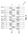
- FIG. 11 is a diagram of an illustrative drive matrix 166 for the three-color pixel element arrangement 164 .
- the illustrative drive matrix 78 shown in FIG. 11 consists of a 2 ⁇ 10 drive matrix, where eight column drivers drive the eight red and eight green emitters coupled to column lines and two column drivers drive the four blue emitters coupled to column lines.
- a first column driver 178 drives the red emitter 170 a and the green emitter 172 a .
- the blue emitters 168 a and 168 c are tied together and driven by a second column driver 180 .
- a third column driver 182 drives the green emitter 174 a and the red emitter 176 a
- a fourth column driver 184 drives the red emitter 170 b and the green emitter 172 b
- a fifth column driver 186 drives the blue emitter 168 b , which is tied together with 168 d .
- the green emitter 174 b and the red emitter 176 b are driven by a sixth column driver 188 , while a seventh column driver 190 drives red emitter 170 c and green emitter 172 c .
- An eighth column driver 192 drives green emitter 174 c and red emitter 176 c
- a ninth column driver 194 drives red emitter 170 d and green emitter 172 d .
- a tenth column driver 196 drives green emitter 174 d and red emitter 176 d.
- the row drivers drive the red, green and blue emitters in each pixel row.
- Row driver 198 drives red emitters 170 a , 170 b , 170 c , and 170 d , green emitters 174 a , 174 b , 174 c , and 174 d , as well as blue emitters 168 c and 168 d .
- Row driver 200 drives green emitters 172 a , 172 b , 172 c , and 172 d , red emitters 176 a , 176 b , 176 c , and 176 d , and blue emitters 168 a and 168 b .
- Each emitter can be driven at continuous luminance values at specific locations in a pixel element, unlike emitters in the prior art, which are driven at discrete luminance values at random locations in a three color pixel element.
- the drive matrix uses approximately 16.6% fewer column drivers to present a given image than does a prior art 2 ⁇ 12-drive matrix for the triad arrangement.
- the column lines are reduced since the blue emitters ( 168 a and 168 c ; 168 b and 168 d ) are combined.
- the driver type, voltage, and timing can be the same as already known in the art for each device technology.
- FIG. 12 is an arrangement 201 of eight three-color pixel elements aligned horizontally, four in each array row.
- Each three-color pixel element can be square-shaped or rectangular-shaped and has two rows with each row including three unit-area polygons, such that an emitter occupies each unit-area polygon.
- At least one unit-area polygon is at least two times the area of the other unit-area polygons and is occupied by blue emitters 210 a , 210 b , 210 c , 210 d , 220 a , and 220 b .
- the blue emitters 210 a , 210 b , 210 c , 210 d , 220 a , and 220 b can be formed as a single emitter or can be two separate blue emitters wired together.
- the blue emitters 210 b and 210 d are staggered such that a smaller blue emitter (the size of the red and green emitters) will be positioned at the edges of the array vertically aligned with the large blue emitter, as illustrated in FIG. 12 .
- blue emitters 222 a , 224 a are vertically disposed on either side of the staggered blue emitter 210 c and blue emitters 222 b , 224 b are vertically disposed on either side of the staggered blue emitter 210 d.
- blue emitters 210 a , 210 b , 210 c , 210 d , 220 a , 220 b , 222 a , 222 b , 224 a , and 224 b are disposed between the red emitters and green emitters.
- Red emitters 202 a , 202 b , 202 c , 202 d are disposed in the first pixel row of the first array row and green emitters 204 a , 204 b , 204 c , and 204 d are disposed in the second pixel row of the first array row to the left of blue emitters 210 a , 210 b , 210 c & 222 a , and 210 d & 222 b of the first, second, third, and fourth three-color pixel elements, respectively.
- Green emitters 206 a , 206 b , 206 c , and 206 d are disposed in the first pixel row of the first array row and red emitters 208 a , 208 b , 208 c , and 208 d are disposed in the second pixel row of the first array row to the right of blue emitters 210 a , 210 b , 210 c & 222 a , and 210 d & 222 b of the first, second, third, and fourth three-color pixel elements, respectively.
- Red emitters 212 a , 212 b , 212 c , and 212 d are disposed in the first pixel row of the second array row and green emitters 214 a , 214 b , 214 c , and 214 d are disposed in the second pixel row of the second array row to the left of blue emitters 220 a , 220 b , 220 c & 224 a , and 210 d & 224 b of the first, second, third, and fourth three-color pixel elements, respectively.
- Green emitters 216 a , 216 b , 216 c , and 216 d are disposed in the first pixel row of the second array row and red emitters 218 a , 218 b , 218 c , and 218 d are disposed in the second pixel row of the second array row to the right of blue emitters 220 a , 220 b , 220 c & 224 a , and 210 d & 224 b of the first, second, third, and fourth three-color pixel elements, respectively.
- the large blue emitters are staggered throughout the array, which requires having smaller blue emitters at the edges vertically aligned with the larger blue emitters.
- FIG. 13 is a diagram of an illustrative drive matrix 254 for the three-color pixel element arrangement 201 illustrated in FIG. 12 .
- the illustrative drive matrix 254 shown in FIG. 13 consists of a 2 ⁇ 10 drive matrix, where eight column drivers drive the sixteen red and sixteen green emitters coupled to column lines and two column drivers drive the ten blue emitters coupled to column lines.
- a first column driver 234 drives the red emitters 202 a , 212 a and the green emitters 204 a , 214 a .
- the blue emitters 210 a , 220 a are tied together with blue emitters 222 a , 210 c , 224 a and are driven by a second column driver 236 .
- a third column driver 238 drives the green emitters 206 a , 216 a and the red emitters 208 a , 218 a
- a fourth column driver 240 drives the red emitters 202 b , 212 b and the green emitters 204 b , 214 b
- a fifth column driver 242 drives the blue emitters 210 b , 220 b , which is tied together with 222 b , 210 d , 224 b .
- the green emitters 206 b , 216 b and the red emitters 208 b , 218 b are driven by a sixth column driver 244 , while a seventh column driver 246 drives red emitters 202 c , 212 c and green emitters 204 c , 214 c .
- An eighth column driver 248 drives green emitters 206 c , 216 c and red emitters 208 c , 218 c
- a ninth column driver 250 drives red emitters 202 d , 212 d and green emitters 204 d , 214 d .
- a tenth column driver 252 drives green emitters 206 d , 216 d and red emitters 208 d , 218 d.
- Row driver 226 drives red emitters 202 a , 202 b , 202 c , and 202 d , green emitters 206 a , 206 b , 206 c , and 206 d , as well as blue emitters 210 a , 210 b , 222 a , 222 b .
- Row driver 228 drives green emitters 204 a , 204 b , 204 c , and 204 d , red emitters 208 a , 208 b , 208 c , and 208 d , and blue emitters 210 c , 210 d .
- Row driver 230 drives red emitters 212 a , 212 b , 212 c , and 212 d , green emitters 216 a , 216 b , 216 c , and 216 d , as well as blue emitters 220 a , 220 b .
- Row driver 232 drives green emitters 214 a , 214 b , 214 c , and 214 d , red emitters 218 a , 218 b , 218 c , and 218 d , and blue emitters 224 a , 224 b .
- Each emitter can be driven at continuous luminance values at specific locations in a three-color pixel element, unlike emitters in the prior art, which are driven at discrete luminance values at random locations in a three color pixel element.
- the drive matrix uses approximately 16.6% fewer column drivers to present a given image than does a prior art 2 ⁇ 12-drive matrix for the triad arrangement.
- the column lines are reduced since the blue emitters ( 210 a , 220 a and 210 c , 222 a , 224 a ; 210 b , 220 b and 210 d , 222 b , 224 b ) are combined.
- the driver type, voltage, and timing can be the same as already known in the art for each device technology.
- Dot inversion is the preferred method of choice for driving panels having the arrangement of columns and rows as discussed above.
- Each blue, red and green emitter is driven with alternating polarities. For example, in a first drive event, a red emitter is driven with a positive voltage and at the next drive event, the same red emitter is driven with a negative voltage.
- FIGS. 6 , 8 , 10 , and 12 that connect the column line of the blue emitter of the first three-color pixel element with its next nearest neighboring three-color pixel element (e.g., the blue emitter of the third three-color pixel element).
- the blue emitter of the second three-color pixel element is coupled with its next nearest neighboring three-color pixel element (e.g., the blue emitter of the fourth three-color pixel element).
- the “next nearest neighboring” three-color pixel element can be construed as being every other blue emitter of a pair of three-color pixel elements coupled together.
- the first three-color pixel element is connected with the third three-color pixel element
- the second three-color pixel element is connected with the fourth three-color pixel element
- the fifth three-color pixel element is connected with the seventh three-color pixel element
- the sixth three-color pixel element is connected with the eight three-color pixel element, etc. In this case, any incidence of “flicker” is reduced or eliminated.
- every column line must be driven with a signal of polarity opposite of its neighbors to guarantee, that should any crosstalk occur, it would be the same for each column. If the array is not driven in this way, asymmetrical crosstalk will result in visible artifacts across the screen. Also, nearby red and green emitters of separate pixel elements must be driven by signals of the opposite polarity to ensure that “flicker” will not occur.
- FIG. 14 illustrates the polarities of the red, green, and blue emitters on the same arrangement in FIG. 6 .
- green emitter 56 a (having a positive value) must have an opposite polarity than red emitter 52 b (having a negative value).
- This arrangement eliminates “flicker” since the column line connects one blue emitter with the blue emitter of its next nearest neighboring three-color pixel element.
- the polarities shown on the blue emitters are those of the column lines, not the polarities stored on the blue emitter.
- the polarity of the blue emitter is determined by the row that is actively addressing the blue emitter, which is connected to the blue emitter of its next nearest neighboring three-color pixel element.
- FIGS. 15 and 16 Additional examples illustrating separate dot inversion schemes by the polarities of the red, green, and blue emitters are found in FIGS. 15 and 16 . Both FIGS. 15 and 16 are based on the arrangement 114 illustrated in FIG. 8 , including another horizontal arrangement ( FIG. 15 , 115 ; FIG. 16 , 314 ).
- red emitter 120 a (having a positive value) must be driven by signals of an opposite polarity than the polarity of the green emitter 122 a (having a negative value).
- Blue emitter 130 a (having a negative value) must be driven by signals of an opposite polarity than the polarity of the blue emitter 132 a (having a positive value).
- Red emitter 124 a (having a positive value) must be driven by signals of an opposite polarity than the polarity of the green emitter 126 a (having a negative value).
- the same polarities are duplicated in the additional horizontal arrangement 115 . This arrangement also eliminates “flicker” since the column lines connect one blue emitter with the blue emitter of its next nearest neighboring three-color pixel element.
- red emitters 120 a and 126 a and green emitters 122 a and 124 a (having positive values) must be driven by signals of an opposite polarity than the polarity of the signals driving the red emitters 302 a and 308 a and green emitters 304 a and 306 a (having negative values).
- blue emitters 130 a and 132 a (having positive values) and blue emitters 310 a and 312 a (having negative values).
- This arrangement also eliminates “flicker” since the column lines connect one blue emitter with the blue emitter of its next nearest neighboring three-color pixel element.
- FIG. 17 Another example that illustrates dot inversion by the polarities of the red, green, and blue emitters is found in FIG. 17 , which is based on the arrangement 164 illustrated in FIG. 10 , including another horizontal arrangement 364 .
- red emitter 170 a and green emitter 174 a (having positive values) and green emitter 172 a and red emitter 176 a (having negative values) must be driven by signals of the same polarity as red emitter 370 a and green emitter 374 a (having positive values) and green emitter 372 a and red emitter 376 a (having negative values), respectively.
- Blue emitter 168 a (having a positive value) must be driven by signals of an opposite polarity than blue emitter 368 a (having a negative value). This arrangement also eliminates “flicker” since the column lines connect a blue emitter with the blue emitter of its next nearest neighboring three-color pixel element.
- red emitters 170 a , 176 a and green emitters 172 a , 174 a must be driven by signals of an opposite polarity than the polarity of red emitters 370 a , 376 a and green emitters 372 a , 374 a (having negative values).
- blue emitter 168 a having a negative value
- blue emitter 368 a having a positive value
- FIG. 19 Another example that illustrates dot inversion by the polarities of the red, green, and blue emitters is found in FIG. 19 , which is based on the arrangement 201 illustrated in FIG. 12 .
- Blue emitter 210 a (having a positive value with a stored negative value) must be driven by signals of an opposite polarity than blue emitter 220 a (having a negative value with a stored positive value).
- Blue emitter 210 c (having a positive value with a stored negative value) must be driven by signals of an opposite polarity than blue emitter 220 c (having a negative value with a stored positive value).
- blue emitters 222 a and 224 b must be driven by signals of an opposite polarity than blue emitters 222 b and 224 a .
- An individual skilled in the art will appreciate the polarities as described herein. This arrangement also eliminates “flicker” since the column lines connect a blue emitter with the blue emitter of its next nearest neighboring three-color pixel element.
- red emitters 202 a , 208 a and green emitters 204 a , 206 a (having positive values) must be driven by signals of an opposite polarity than red emitters 212 a , 218 a and green emitters 214 a , 216 a (having negative values).
- blue emitter 210 a (having a negative value with a stored positive value)
- blue emitter 220 a (having a positive value with a stored negative value).
- Blue emitter 210 c (having a negative value with a stored positive value) must be driven by signals of an opposite polarity than blue emitter 220 c (having a positive value with a stored negative value). While blue emitters 222 a and 224 b must be driven by signals of an opposite polarity than blue emitters 222 b and 224 a .
- An individual skilled in the art will appreciate the polarities as described herein. This arrangement also eliminates “flicker” since the column lines connect a blue emitter with the blue emitter of its next nearest neighboring three-color pixel element.
- the three-color pixel element can be operated by appropriately driving the individual emitters. A voltage is applied through each row and column driver to each individual row line and column line. At this point, each emitter is illuminated, according to the proper voltage, to create an image on the display.
Abstract
Description
Claims (6)
Priority Applications (1)
| Application Number | Priority Date | Filing Date | Title |
|---|---|---|---|
| US11/072,814 US7728802B2 (en) | 2000-07-28 | 2005-03-04 | Arrangements of color pixels for full color imaging devices with simplified addressing |
Applications Claiming Priority (3)
| Application Number | Priority Date | Filing Date | Title |
|---|---|---|---|
| US09/628,122 US7274383B1 (en) | 2000-07-28 | 2000-07-28 | Arrangement of color pixels for full color imaging devices with simplified addressing |
| US09/916,232 US6903754B2 (en) | 2000-07-28 | 2001-07-25 | Arrangement of color pixels for full color imaging devices with simplified addressing |
| US11/072,814 US7728802B2 (en) | 2000-07-28 | 2005-03-04 | Arrangements of color pixels for full color imaging devices with simplified addressing |
Related Parent Applications (1)
| Application Number | Title | Priority Date | Filing Date |
|---|---|---|---|
| US09/916,232 Continuation US6903754B2 (en) | 2000-07-28 | 2001-07-25 | Arrangement of color pixels for full color imaging devices with simplified addressing |
Publications (2)
| Publication Number | Publication Date |
|---|---|
| US20050174363A1 US20050174363A1 (en) | 2005-08-11 |
| US7728802B2 true US7728802B2 (en) | 2010-06-01 |
Family
ID=27090623
Family Applications (1)
| Application Number | Title | Priority Date | Filing Date |
|---|---|---|---|
| US11/072,814 Expired - Fee Related US7728802B2 (en) | 2000-07-28 | 2005-03-04 | Arrangements of color pixels for full color imaging devices with simplified addressing |
Country Status (5)
| Country | Link |
|---|---|
| US (1) | US7728802B2 (en) |
| EP (1) | EP1314149B1 (en) |
| CN (1) | CN100401359C (en) |
| AU (1) | AU2001280892A1 (en) |
| WO (1) | WO2002011112A2 (en) |
Cited By (5)
| Publication number | Priority date | Publication date | Assignee | Title |
|---|---|---|---|---|
| US20090121983A1 (en) * | 2007-11-13 | 2009-05-14 | Samsung Electronics Co., Ltd. | Organic light emitting diode display and method for manufacturing the same |
| US20150015466A1 (en) * | 2013-07-12 | 2015-01-15 | Everdisplay Optronics (Shanghai) Limited | Pixel array, display and method for presenting image on the display |
| US9099025B2 (en) | 2012-05-17 | 2015-08-04 | Samsung Display Co., Ltd. | Data rendering method, data rendering device, and display panel with subpixel rendering structure using the same |
| US20160203800A1 (en) * | 2015-01-13 | 2016-07-14 | Boe Technology Group Co., Ltd. | Display method of display panel, display panel and display device |
| US10417950B2 (en) | 2018-02-06 | 2019-09-17 | Tectus Corporation | Subpixel layouts for eye-mounted displays |
Families Citing this family (33)
| Publication number | Priority date | Publication date | Assignee | Title |
|---|---|---|---|---|
| US7274383B1 (en) * | 2000-07-28 | 2007-09-25 | Clairvoyante, Inc | Arrangement of color pixels for full color imaging devices with simplified addressing |
| US7123277B2 (en) | 2001-05-09 | 2006-10-17 | Clairvoyante, Inc. | Conversion of a sub-pixel format data to another sub-pixel data format |
| EP2273481A3 (en) | 2001-06-11 | 2012-02-22 | Genoa Color Technologies Ltd. | Device, system and method for color display |
| US8289266B2 (en) | 2001-06-11 | 2012-10-16 | Genoa Color Technologies Ltd. | Method, device and system for multi-color sequential LCD panel |
| US7714824B2 (en) | 2001-06-11 | 2010-05-11 | Genoa Color Technologies Ltd. | Multi-primary display with spectrally adapted back-illumination |
| US7079164B2 (en) * | 2001-08-03 | 2006-07-18 | Lg.Philips Lcd Co., Ltd. | Method and apparatus for driving liquid crystal display panel |
| KR100870003B1 (en) * | 2001-12-24 | 2008-11-24 | 삼성전자주식회사 | a liquid crystal display |
| US7755652B2 (en) | 2002-01-07 | 2010-07-13 | Samsung Electronics Co., Ltd. | Color flat panel display sub-pixel rendering and driver configuration for sub-pixel arrangements with split sub-pixels |
| US7417648B2 (en) | 2002-01-07 | 2008-08-26 | Samsung Electronics Co. Ltd., | Color flat panel display sub-pixel arrangements and layouts for sub-pixel rendering with split blue sub-pixels |
| US20040051724A1 (en) | 2002-09-13 | 2004-03-18 | Elliott Candice Hellen Brown | Four color arrangements of emitters for subpixel rendering |
| US7583279B2 (en) | 2004-04-09 | 2009-09-01 | Samsung Electronics Co., Ltd. | Subpixel layouts and arrangements for high brightness displays |
| US9953590B2 (en) | 2002-04-11 | 2018-04-24 | Samsung Display Co., Ltd. | Color display devices and methods with enhanced attributes |
| KR100878280B1 (en) | 2002-11-20 | 2009-01-13 | 삼성전자주식회사 | Liquid crystal displays using 4 color and panel for the same |
| KR20040080778A (en) | 2003-03-13 | 2004-09-20 | 삼성전자주식회사 | Liquid crystal displays using 4 color and panel for the same |
| US7791679B2 (en) | 2003-06-06 | 2010-09-07 | Samsung Electronics Co., Ltd. | Alternative thin film transistors for liquid crystal displays |
| KR100580624B1 (en) * | 2003-09-19 | 2006-05-16 | 삼성전자주식회사 | Method and apparatus for displaying image, and computer-readable recording media for storing computer program |
| KR101012788B1 (en) * | 2003-10-16 | 2011-02-08 | 삼성전자주식회사 | Liquid crystal display and driving method thereof |
| CN103177701A (en) | 2003-12-15 | 2013-06-26 | 格诺色彩技术有限公司 | Multi-primary liquid crystal display |
| US7495722B2 (en) | 2003-12-15 | 2009-02-24 | Genoa Color Technologies Ltd. | Multi-color liquid crystal display |
| US7248268B2 (en) | 2004-04-09 | 2007-07-24 | Clairvoyante, Inc | Subpixel rendering filters for high brightness subpixel layouts |
| US7705855B2 (en) | 2005-06-15 | 2010-04-27 | Samsung Electronics Co., Ltd. | Bichromatic display |
| US20080001525A1 (en) * | 2006-06-30 | 2008-01-03 | Au Optronics Corporation | Arrangements of color pixels for full color OLED |
| US7876341B2 (en) | 2006-08-28 | 2011-01-25 | Samsung Electronics Co., Ltd. | Subpixel layouts for high brightness displays and systems |
| US8018476B2 (en) | 2006-08-28 | 2011-09-13 | Samsung Electronics Co., Ltd. | Subpixel layouts for high brightness displays and systems |
| US7567370B2 (en) * | 2007-07-26 | 2009-07-28 | Hewlett-Packard Development Company, L.P. | Color display having layer dependent spatial resolution and related method |
| US8350940B2 (en) * | 2009-06-08 | 2013-01-08 | Aptina Imaging Corporation | Image sensors and color filter arrays for charge summing and interlaced readout modes |
| FR2966632B1 (en) * | 2010-10-22 | 2016-12-30 | Microoled | MATRIX DISPLAY DEVICE OF TWO MERGED IMAGES |
| KR101862793B1 (en) * | 2012-08-08 | 2018-05-31 | 삼성디스플레이 주식회사 | Pixel Array Structure and Organic Light Emitting Display including The Same |
| CN105006479B (en) * | 2014-04-23 | 2018-04-20 | 群创光电股份有限公司 | Display base plate and apply its display device |
| CN104617125B (en) * | 2015-01-16 | 2018-01-19 | 信利(惠州)智能显示有限公司 | A kind of OLED pixel arrangement architecture |
| CN104616597B (en) * | 2015-02-13 | 2017-03-29 | 京东方科技集团股份有限公司 | Display base plate and its driving method and display device |
| CN104617131B (en) | 2015-02-15 | 2019-10-01 | 京东方科技集团股份有限公司 | A kind of pixel arrangement structure and display device |
| CN110133886A (en) | 2018-02-09 | 2019-08-16 | 京东方科技集团股份有限公司 | Pixel arrangement structure, display base plate and display device |
Citations (122)
| Publication number | Priority date | Publication date | Assignee | Title |
|---|---|---|---|---|
| US3971065A (en) | 1975-03-05 | 1976-07-20 | Eastman Kodak Company | Color imaging array |
| US4353062A (en) | 1979-05-04 | 1982-10-05 | U.S. Philips Corporation | Modulator circuit for a matrix display device |
| GB2133912A (en) | 1982-12-15 | 1984-08-01 | Citizen Watch Co Ltd | Color display device |
| GB2146478A (en) | 1983-09-08 | 1985-04-17 | Sharp Kk | LCD display devices |
| EP0158366A2 (en) | 1984-04-13 | 1985-10-16 | Sharp Kabushiki Kaisha | Color liquid-crystal display apparatus |
| US4593978A (en) | 1983-03-18 | 1986-06-10 | Thomson-Csf | Smectic liquid crystal color display screen |
| EP0203005A1 (en) | 1985-05-20 | 1986-11-26 | Roger Menn | Tricolour electroluminescent matrix screen and method for its manufacture |
| US4751535A (en) | 1986-10-15 | 1988-06-14 | Xerox Corporation | Color-matched printing |
| US4773737A (en) | 1984-12-17 | 1988-09-27 | Canon Kabushiki Kaisha | Color display panel |
| US4786964A (en) | 1987-02-02 | 1988-11-22 | Polaroid Corporation | Electronic color imaging apparatus with prismatic color filter periodically interposed in front of an array of primary color filters |
| US4792728A (en) | 1985-06-10 | 1988-12-20 | International Business Machines Corporation | Cathodoluminescent garnet lamp |
| US4800375A (en) | 1986-10-24 | 1989-01-24 | Honeywell Inc. | Four color repetitive sequence matrix array for flat panel displays |
| EP0322106A2 (en) | 1987-11-28 | 1989-06-28 | THORN EMI plc | Display device |
| US4853592A (en) | 1988-03-10 | 1989-08-01 | Rockwell International Corporation | Flat panel display having pixel spacing and luminance levels providing high resolution |
| US4886343A (en) | 1988-06-20 | 1989-12-12 | Honeywell Inc. | Apparatus and method for additive/subtractive pixel arrangement in color mosaic displays |
| US4908609A (en) | 1986-04-25 | 1990-03-13 | U.S. Philips Corporation | Color display device |
| US4920409A (en) | 1987-06-23 | 1990-04-24 | Casio Computer Co., Ltd. | Matrix type color liquid crystal display device |
| US4965565A (en) | 1987-05-06 | 1990-10-23 | Nec Corporation | Liquid crystal display panel having a thin-film transistor array for displaying a high quality picture |
| US4966441A (en) | 1989-03-28 | 1990-10-30 | In Focus Systems, Inc. | Hybrid color display system |
| US4967264A (en) | 1989-05-30 | 1990-10-30 | Eastman Kodak Company | Color sequential optical offset image sampling system |
| US5006840A (en) | 1984-04-13 | 1991-04-09 | Sharp Kabushiki Kaisha | Color liquid-crystal display apparatus with rectilinear arrangement |
| US5052785A (en) | 1989-07-07 | 1991-10-01 | Fuji Photo Film Co., Ltd. | Color liquid crystal shutter having more green electrodes than red or blue electrodes |
| US5113274A (en) | 1988-06-13 | 1992-05-12 | Mitsubishi Denki Kabushiki Kaisha | Matrix-type color liquid crystal display device |
| US5132674A (en) | 1987-10-22 | 1992-07-21 | Rockwell International Corporation | Method and apparatus for drawing high quality lines on color matrix displays |
| US5184114A (en) | 1982-11-04 | 1993-02-02 | Integrated Systems Engineering, Inc. | Solid state color display system and light emitting diode pixels therefor |
| US5189404A (en) | 1986-06-18 | 1993-02-23 | Hitachi, Ltd. | Display apparatus with rotatable display screen |
| US5233385A (en) | 1991-12-18 | 1993-08-03 | Texas Instruments Incorporated | White light enhanced color field sequential projection |
| US5311337A (en) | 1992-09-23 | 1994-05-10 | Honeywell Inc. | Color mosaic matrix display having expanded or reduced hexagonal dot pattern |
| US5315418A (en) | 1992-06-17 | 1994-05-24 | Xerox Corporation | Two path liquid crystal light valve color display with light coupling lens array disposed along the red-green light path |
| US5334996A (en) | 1989-12-28 | 1994-08-02 | U.S. Philips Corporation | Color display apparatus |
| US5341153A (en) | 1988-06-13 | 1994-08-23 | International Business Machines Corporation | Method of and apparatus for displaying a multicolor image |
| US5398066A (en) | 1993-07-27 | 1995-03-14 | Sri International | Method and apparatus for compression and decompression of digital color images |
| US5436747A (en) | 1990-08-16 | 1995-07-25 | International Business Machines Corporation | Reduced flicker liquid crystal display |
| US5461503A (en) | 1993-04-08 | 1995-10-24 | Societe D'applications Generales D'electricite Et De Mecanique Sagem | Color matrix display unit with double pixel area for red and blue pixels |
| US5535028A (en) | 1993-04-03 | 1996-07-09 | Samsung Electronics Co., Ltd. | Liquid crystal display panel having nonrectilinear data lines |
| US5541653A (en) | 1993-07-27 | 1996-07-30 | Sri International | Method and appartus for increasing resolution of digital color images using correlated decoding |
| US5561460A (en) | 1993-06-02 | 1996-10-01 | Hamamatsu Photonics K.K. | Solid-state image pick up device having a rotating plate for shifting position of the image on a sensor array |
| US5563621A (en) | 1991-11-18 | 1996-10-08 | Black Box Vision Limited | Display apparatus |
| US5579027A (en) | 1992-01-31 | 1996-11-26 | Canon Kabushiki Kaisha | Method of driving image display apparatus |
| US5646702A (en) | 1994-10-31 | 1997-07-08 | Honeywell Inc. | Field emitter liquid crystal display |
| US5648793A (en) | 1992-01-08 | 1997-07-15 | Industrial Technology Research Institute | Driving system for active matrix liquid crystal display |
| EP0793214A1 (en) | 1996-02-29 | 1997-09-03 | Texas Instruments Incorporated | Display system with spatial light modulator with decompression of input image signal |
| EP0812114A1 (en) | 1995-12-21 | 1997-12-10 | Sony Corporation | Solid-state image sensor, method for driving the same, and solid-state camera device and camera system |
| US5729244A (en) | 1995-04-04 | 1998-03-17 | Lockwood; Harry F. | Field emission device with microchannel gain element |
| US5754226A (en) | 1994-12-20 | 1998-05-19 | Sharp Kabushiki Kaisha | Imaging apparatus for obtaining a high resolution image |
| US5773927A (en) | 1995-08-30 | 1998-06-30 | Micron Display Technology, Inc. | Field emission display device with focusing electrodes at the anode and method for constructing same |
| US5792579A (en) | 1996-03-12 | 1998-08-11 | Flex Products, Inc. | Method for preparing a color filter |
| US5815101A (en) | 1996-08-02 | 1998-09-29 | Fonte; Gerard C. A. | Method and system for removing and/or measuring aliased signals |
| US5821913A (en) | 1994-12-14 | 1998-10-13 | International Business Machines Corporation | Method of color image enlargement in which each RGB subpixel is given a specific brightness weight on the liquid crystal display |
| US5856050A (en) | 1996-09-24 | 1999-01-05 | Fuji Photo Film Co., Ltd. | Coverage of pixel sheet with protective layer |
| EP0899604A2 (en) | 1997-08-28 | 1999-03-03 | Canon Kabushiki Kaisha | Color display apparatus |
| DE19746329A1 (en) | 1997-09-13 | 1999-03-18 | Gia Chuong Dipl Ing Phan | Display device for e.g. video |
| US5936596A (en) * | 1994-09-02 | 1999-08-10 | Sharp Kabushiki Kaisha | Two-dimensional image display device and driving circuit |
| US5949496A (en) | 1996-08-28 | 1999-09-07 | Samsung Electronics Co., Ltd. | Color correction device for correcting color distortion and gamma characteristic |
| DE29909537U1 (en) | 1999-05-31 | 1999-09-09 | Phan Gia Chuong | Display and its control |
| US5973664A (en) | 1998-03-19 | 1999-10-26 | Portrait Displays, Inc. | Parameterized image orientation for computer displays |
| US6002446A (en) | 1997-02-24 | 1999-12-14 | Paradise Electronics, Inc. | Method and apparatus for upscaling an image |
| US6005692A (en) | 1997-05-29 | 1999-12-21 | Stahl; Thomas D. | Light-emitting diode constructions |
| US6008868A (en) | 1994-03-11 | 1999-12-28 | Canon Kabushiki Kaisha | Luminance weighted discrete level display |
| US6034666A (en) | 1996-10-16 | 2000-03-07 | Mitsubishi Denki Kabushiki Kaisha | System and method for displaying a color picture |
| US6037719A (en) | 1998-04-09 | 2000-03-14 | Hughes Electronics Corporation | Matrix-addressed display having micromachined electromechanical switches |
| US6038031A (en) | 1997-07-28 | 2000-03-14 | 3Dlabs, Ltd | 3D graphics object copying with reduced edge artifacts |
| US6049626A (en) | 1996-10-09 | 2000-04-11 | Samsung Electronics Co., Ltd. | Image enhancing method and circuit using mean separate/quantized mean separate histogram equalization and color compensation |
| US6061533A (en) | 1997-12-01 | 2000-05-09 | Matsushita Electric Industrial Co., Ltd. | Gamma correction for apparatus using pre and post transfer image density |
| US6064363A (en) | 1997-04-07 | 2000-05-16 | Lg Semicon Co., Ltd. | Driving circuit and method thereof for a display device |
| US6072272A (en) | 1998-05-04 | 2000-06-06 | Motorola, Inc. | Color flat panel display device |
| US6097367A (en) | 1996-09-06 | 2000-08-01 | Matsushita Electric Industrial Co., Ltd. | Display device |
| US6108122A (en) | 1998-04-29 | 2000-08-22 | Sharp Kabushiki Kaisha | Light modulating devices |
| US6144352A (en) | 1997-05-15 | 2000-11-07 | Matsushita Electric Industrial Co., Ltd. | LED display device and method for controlling the same |
| US6147664A (en) | 1997-08-29 | 2000-11-14 | Candescent Technologies Corporation | Controlling the brightness of an FED device using PWM on the row side and AM on the column side |
| US6151001A (en) | 1998-01-30 | 2000-11-21 | Electro Plasma, Inc. | Method and apparatus for minimizing false image artifacts in a digitally controlled display monitor |
| DE19923527A1 (en) | 1999-05-21 | 2000-11-23 | Leurocom Visuelle Informations | Display device for characters and symbols using matrix of light emitters, excites emitters of mono colors in multiplex phases |
| US6160535A (en) | 1997-06-16 | 2000-12-12 | Samsung Electronics Co., Ltd. | Liquid crystal display devices capable of improved dot-inversion driving and methods of operation thereof |
| US6184903B1 (en) | 1996-12-27 | 2001-02-06 | Sony Corporation | Apparatus and method for parallel rendering of image pixels |
| WO2001010112A2 (en) | 1999-07-30 | 2001-02-08 | Microsoft Corporation | Methods and apparatus for filtering and caching data representing images |
| US6188385B1 (en) | 1998-10-07 | 2001-02-13 | Microsoft Corporation | Method and apparatus for displaying images such as text |
| EP1083539A2 (en) | 1999-09-08 | 2001-03-14 | Victor Company Of Japan, Ltd. | Image displaying with multi-gradation processing |
| WO2001029817A1 (en) | 1999-10-19 | 2001-04-26 | Intensys Corporation | Improving image display quality by adaptive subpixel rendering |
| US6225967B1 (en) | 1996-06-19 | 2001-05-01 | Alps Electric Co., Ltd. | Matrix-driven display apparatus and a method for driving the same |
| US6225973B1 (en) | 1998-10-07 | 2001-05-01 | Microsoft Corporation | Mapping samples of foreground/background color image data to pixel sub-components |
| US6236390B1 (en) | 1998-10-07 | 2001-05-22 | Microsoft Corporation | Methods and apparatus for positioning displayed characters |
| US6243070B1 (en) | 1998-10-07 | 2001-06-05 | Microsoft Corporation | Method and apparatus for detecting and reducing color artifacts in images |
| US6243055B1 (en) * | 1994-10-25 | 2001-06-05 | James L. Fergason | Optical display system and method with optical shifting of pixel position including conversion of pixel layout to form delta to stripe pattern by time base multiplexing |
| US6262710B1 (en) | 1999-05-25 | 2001-07-17 | Intel Corporation | Performing color conversion in extended color polymer displays |
| WO2001052546A2 (en) | 2000-01-10 | 2001-07-19 | Koninklijke Philips Electronics N.V. | Image interpolation and decimation using a continuously variable delay filter and combined with a polyphase filter |
| JP2001203919A (en) | 2000-01-17 | 2001-07-27 | Minolta Co Ltd | Digital camera |
| US6271891B1 (en) | 1998-06-19 | 2001-08-07 | Pioneer Electronic Corporation | Video signal processing circuit providing optimum signal level for inverse gamma correction |
| DE20109354U1 (en) | 2000-06-27 | 2001-08-09 | Giantplus Technology Co | Color flat screen with two-color filter |
| US20010017515A1 (en) | 2000-02-29 | 2001-08-30 | Toshiaki Kusunoki | Display device using thin film cathode and its process |
| US6299329B1 (en) | 1999-02-23 | 2001-10-09 | Hewlett-Packard Company | Illumination source for a scanner having a plurality of solid state lamps and a related method |
| US20010040645A1 (en) | 2000-02-01 | 2001-11-15 | Shunpei Yamazaki | Semiconductor device and manufacturing method thereof |
| US6327008B1 (en) | 1995-12-12 | 2001-12-04 | Lg Philips Co. Ltd. | Color liquid crystal display unit |
| US20020012071A1 (en) | 2000-04-21 | 2002-01-31 | Xiuhong Sun | Multispectral imaging system with spatial resolution enhancement |
| US20020015110A1 (en) | 2000-07-28 | 2002-02-07 | Clairvoyante Laboratories, Inc. | Arrangement of color pixels for full color imaging devices with simplified addressing |
| US6346972B1 (en) | 1999-05-26 | 2002-02-12 | Samsung Electronics Co., Ltd. | Video display apparatus with on-screen display pivoting function |
| US20020017645A1 (en) | 2000-05-12 | 2002-02-14 | Semiconductor Energy Laboratory Co., Ltd. | Electro-optical device |
| US6377262B1 (en) | 1999-07-30 | 2002-04-23 | Microsoft Corporation | Rendering sub-pixel precision characters having widths compatible with pixel precision characters |
| US20020050972A1 (en) * | 2000-10-31 | 2002-05-02 | Fujitsu Limited | Dot-inversion data driver for liquid crystal display device |
| US6392717B1 (en) | 1997-05-30 | 2002-05-21 | Texas Instruments Incorporated | High brightness digital display system |
| US6393145B2 (en) | 1999-01-12 | 2002-05-21 | Microsoft Corporation | Methods apparatus and data structures for enhancing the resolution of images to be rendered on patterned display devices |
| WO2002059685A2 (en) | 2001-01-26 | 2002-08-01 | International Business Machines Corporation | Adjusting subpixel intensity values based upon luminance characteristics of the subpixels in liquid crystal displays |
| US6429867B1 (en) | 1999-03-15 | 2002-08-06 | Sun Microsystems, Inc. | System and method for generating and playback of three-dimensional movies |
| US6441867B1 (en) | 1999-10-22 | 2002-08-27 | Sharp Laboratories Of America, Incorporated | Bit-depth extension of digital displays using noise |
| US20020122160A1 (en) | 2000-12-30 | 2002-09-05 | Kunzman Adam J. | Reduced color separation white enhancement for sequential color displays |
| US6453067B1 (en) | 1997-10-20 | 2002-09-17 | Texas Instruments Incorporated | Brightness gain using white segment with hue and gain correction |
| US20020140831A1 (en) | 1997-04-11 | 2002-10-03 | Fuji Photo Film Co. | Image signal processing device for minimizing false signals at color boundaries |
| US6466618B1 (en) | 1999-11-19 | 2002-10-15 | Sharp Laboratories Of America, Inc. | Resolution improvement for multiple images |
| US6486923B1 (en) * | 1999-03-26 | 2002-11-26 | Mitsubishi Denki Kabushiki Kaisha | Color picture display apparatus using hue modification to improve picture quality |
| EP1261014A2 (en) | 2001-05-12 | 2002-11-27 | Philips Corporate Intellectual Property GmbH | Plasma display panel with pixel-forming matrix-array |
| US20030011613A1 (en) | 2001-07-16 | 2003-01-16 | Booth Lawrence A. | Method and apparatus for wide gamut multicolor display |
| WO2003014819A1 (en) | 2001-08-07 | 2003-02-20 | Samsung Electronics Co., Ltd. | A liquid crystal display |
| US20030043567A1 (en) | 2001-08-27 | 2003-03-06 | Hoelen Christoph Gerard August | Light panel with enlarged viewing window |
| US20030071826A1 (en) | 2000-02-02 | 2003-04-17 | Goertzen Kenbe D. | System and method for optimizing image resolution using pixelated imaging device |
| US20030071943A1 (en) | 2001-10-12 | 2003-04-17 | Lg.Philips Lcd., Ltd. | Data wire device of pentile matrix display device |
| US20030090581A1 (en) | 2000-07-28 | 2003-05-15 | Credelle Thomas Lloyd | Color display having horizontal sub-pixel arrangements and layouts |
| US20030117423A1 (en) | 2001-12-14 | 2003-06-26 | Brown Elliott Candice Hellen | Color flat panel display sub-pixel arrangements and layouts with reduced blue luminance well visibility |
| US6628068B1 (en) | 1998-12-12 | 2003-09-30 | Sharp Kabushiki Kaisha | Luminescent device and a liquid crystal device incorporating a luminescent device |
| US20030218618A1 (en) | 1997-09-13 | 2003-11-27 | Phan Gia Chuong | Dynamic pixel resolution, brightness and contrast for displays using spatial elements |
| EP1381020A2 (en) | 1999-04-28 | 2004-01-14 | Barco N.V. | Method for displaying images on a display device, as well as a display device used therefor |
| US6680761B1 (en) | 2000-01-24 | 2004-01-20 | Rainbow Displays, Inc. | Tiled flat-panel display having visually imperceptible seams, optimized for HDTV applications |
| US20040046714A1 (en) | 2001-05-09 | 2004-03-11 | Clairvoyante Laboratories, Inc. | Color flat panel display sub-pixel arrangements and layouts |
| US6850219B2 (en) * | 2000-06-09 | 2005-02-01 | Hitachi, Ltd. | Display device |
-
2001
- 2001-07-26 WO PCT/US2001/023892 patent/WO2002011112A2/en active Application Filing
- 2001-07-26 CN CNB018135153A patent/CN100401359C/en not_active Expired - Lifetime
- 2001-07-26 AU AU2001280892A patent/AU2001280892A1/en not_active Abandoned
- 2001-07-26 EP EP01959324.3A patent/EP1314149B1/en not_active Expired - Lifetime
-
2005
- 2005-03-04 US US11/072,814 patent/US7728802B2/en not_active Expired - Fee Related
Patent Citations (143)
| Publication number | Priority date | Publication date | Assignee | Title |
|---|---|---|---|---|
| US3971065A (en) | 1975-03-05 | 1976-07-20 | Eastman Kodak Company | Color imaging array |
| US4353062A (en) | 1979-05-04 | 1982-10-05 | U.S. Philips Corporation | Modulator circuit for a matrix display device |
| US5184114A (en) | 1982-11-04 | 1993-02-02 | Integrated Systems Engineering, Inc. | Solid state color display system and light emitting diode pixels therefor |
| US4642619A (en) | 1982-12-15 | 1987-02-10 | Citizen Watch Co., Ltd. | Non-light-emitting liquid crystal color display device |
| GB2133912A (en) | 1982-12-15 | 1984-08-01 | Citizen Watch Co Ltd | Color display device |
| US4593978A (en) | 1983-03-18 | 1986-06-10 | Thomson-Csf | Smectic liquid crystal color display screen |
| GB2146478A (en) | 1983-09-08 | 1985-04-17 | Sharp Kk | LCD display devices |
| US4651148A (en) | 1983-09-08 | 1987-03-17 | Sharp Kabushiki Kaisha | Liquid crystal display driving with switching transistors |
| EP0158366A2 (en) | 1984-04-13 | 1985-10-16 | Sharp Kabushiki Kaisha | Color liquid-crystal display apparatus |
| US5144288A (en) | 1984-04-13 | 1992-09-01 | Sharp Kabushiki Kaisha | Color liquid-crystal display apparatus using delta configuration of picture elements |
| US5006840A (en) | 1984-04-13 | 1991-04-09 | Sharp Kabushiki Kaisha | Color liquid-crystal display apparatus with rectilinear arrangement |
| US4773737A (en) | 1984-12-17 | 1988-09-27 | Canon Kabushiki Kaisha | Color display panel |
| EP0203005A1 (en) | 1985-05-20 | 1986-11-26 | Roger Menn | Tricolour electroluminescent matrix screen and method for its manufacture |
| US4874986A (en) | 1985-05-20 | 1989-10-17 | Roger Menn | Trichromatic electroluminescent matrix screen, and method of manufacture |
| US4792728A (en) | 1985-06-10 | 1988-12-20 | International Business Machines Corporation | Cathodoluminescent garnet lamp |
| US4908609A (en) | 1986-04-25 | 1990-03-13 | U.S. Philips Corporation | Color display device |
| US5189404A (en) | 1986-06-18 | 1993-02-23 | Hitachi, Ltd. | Display apparatus with rotatable display screen |
| US4751535A (en) | 1986-10-15 | 1988-06-14 | Xerox Corporation | Color-matched printing |
| US4800375A (en) | 1986-10-24 | 1989-01-24 | Honeywell Inc. | Four color repetitive sequence matrix array for flat panel displays |
| US4786964A (en) | 1987-02-02 | 1988-11-22 | Polaroid Corporation | Electronic color imaging apparatus with prismatic color filter periodically interposed in front of an array of primary color filters |
| US4965565A (en) | 1987-05-06 | 1990-10-23 | Nec Corporation | Liquid crystal display panel having a thin-film transistor array for displaying a high quality picture |
| US4920409A (en) | 1987-06-23 | 1990-04-24 | Casio Computer Co., Ltd. | Matrix type color liquid crystal display device |
| US5132674A (en) | 1987-10-22 | 1992-07-21 | Rockwell International Corporation | Method and apparatus for drawing high quality lines on color matrix displays |
| EP0322106A2 (en) | 1987-11-28 | 1989-06-28 | THORN EMI plc | Display device |
| US4853592A (en) | 1988-03-10 | 1989-08-01 | Rockwell International Corporation | Flat panel display having pixel spacing and luminance levels providing high resolution |
| US5113274A (en) | 1988-06-13 | 1992-05-12 | Mitsubishi Denki Kabushiki Kaisha | Matrix-type color liquid crystal display device |
| US5341153A (en) | 1988-06-13 | 1994-08-23 | International Business Machines Corporation | Method of and apparatus for displaying a multicolor image |
| US4886343A (en) | 1988-06-20 | 1989-12-12 | Honeywell Inc. | Apparatus and method for additive/subtractive pixel arrangement in color mosaic displays |
| US4966441A (en) | 1989-03-28 | 1990-10-30 | In Focus Systems, Inc. | Hybrid color display system |
| US4967264A (en) | 1989-05-30 | 1990-10-30 | Eastman Kodak Company | Color sequential optical offset image sampling system |
| US5052785A (en) | 1989-07-07 | 1991-10-01 | Fuji Photo Film Co., Ltd. | Color liquid crystal shutter having more green electrodes than red or blue electrodes |
| US5334996A (en) | 1989-12-28 | 1994-08-02 | U.S. Philips Corporation | Color display apparatus |
| US5436747A (en) | 1990-08-16 | 1995-07-25 | International Business Machines Corporation | Reduced flicker liquid crystal display |
| US5563621A (en) | 1991-11-18 | 1996-10-08 | Black Box Vision Limited | Display apparatus |
| US5233385A (en) | 1991-12-18 | 1993-08-03 | Texas Instruments Incorporated | White light enhanced color field sequential projection |
| US5648793A (en) | 1992-01-08 | 1997-07-15 | Industrial Technology Research Institute | Driving system for active matrix liquid crystal display |
| US5579027A (en) | 1992-01-31 | 1996-11-26 | Canon Kabushiki Kaisha | Method of driving image display apparatus |
| US5315418A (en) | 1992-06-17 | 1994-05-24 | Xerox Corporation | Two path liquid crystal light valve color display with light coupling lens array disposed along the red-green light path |
| US5311337A (en) | 1992-09-23 | 1994-05-10 | Honeywell Inc. | Color mosaic matrix display having expanded or reduced hexagonal dot pattern |
| US5535028A (en) | 1993-04-03 | 1996-07-09 | Samsung Electronics Co., Ltd. | Liquid crystal display panel having nonrectilinear data lines |
| US5461503A (en) | 1993-04-08 | 1995-10-24 | Societe D'applications Generales D'electricite Et De Mecanique Sagem | Color matrix display unit with double pixel area for red and blue pixels |
| US5561460A (en) | 1993-06-02 | 1996-10-01 | Hamamatsu Photonics K.K. | Solid-state image pick up device having a rotating plate for shifting position of the image on a sensor array |
| US5398066A (en) | 1993-07-27 | 1995-03-14 | Sri International | Method and apparatus for compression and decompression of digital color images |
| US5541653A (en) | 1993-07-27 | 1996-07-30 | Sri International | Method and appartus for increasing resolution of digital color images using correlated decoding |
| EP0671650B1 (en) | 1994-03-11 | 2002-09-25 | Canon Kabushiki Kaisha | A luminance weighted discrete level display |
| US6008868A (en) | 1994-03-11 | 1999-12-28 | Canon Kabushiki Kaisha | Luminance weighted discrete level display |
| US5936596A (en) * | 1994-09-02 | 1999-08-10 | Sharp Kabushiki Kaisha | Two-dimensional image display device and driving circuit |
| US6243055B1 (en) * | 1994-10-25 | 2001-06-05 | James L. Fergason | Optical display system and method with optical shifting of pixel position including conversion of pixel layout to form delta to stripe pattern by time base multiplexing |
| US5646702A (en) | 1994-10-31 | 1997-07-08 | Honeywell Inc. | Field emitter liquid crystal display |
| US5821913A (en) | 1994-12-14 | 1998-10-13 | International Business Machines Corporation | Method of color image enlargement in which each RGB subpixel is given a specific brightness weight on the liquid crystal display |
| US5754226A (en) | 1994-12-20 | 1998-05-19 | Sharp Kabushiki Kaisha | Imaging apparatus for obtaining a high resolution image |
| US5729244A (en) | 1995-04-04 | 1998-03-17 | Lockwood; Harry F. | Field emission device with microchannel gain element |
| US5773927A (en) | 1995-08-30 | 1998-06-30 | Micron Display Technology, Inc. | Field emission display device with focusing electrodes at the anode and method for constructing same |
| US6327008B1 (en) | 1995-12-12 | 2001-12-04 | Lg Philips Co. Ltd. | Color liquid crystal display unit |
| EP0812114A1 (en) | 1995-12-21 | 1997-12-10 | Sony Corporation | Solid-state image sensor, method for driving the same, and solid-state camera device and camera system |
| US6198507B1 (en) | 1995-12-21 | 2001-03-06 | Sony Corporation | Solid-state imaging device, method of driving solid-state imaging device, camera device, and camera system |
| EP0793214A1 (en) | 1996-02-29 | 1997-09-03 | Texas Instruments Incorporated | Display system with spatial light modulator with decompression of input image signal |
| US5792579A (en) | 1996-03-12 | 1998-08-11 | Flex Products, Inc. | Method for preparing a color filter |
| US6225967B1 (en) | 1996-06-19 | 2001-05-01 | Alps Electric Co., Ltd. | Matrix-driven display apparatus and a method for driving the same |
| US5815101A (en) | 1996-08-02 | 1998-09-29 | Fonte; Gerard C. A. | Method and system for removing and/or measuring aliased signals |
| US5949496A (en) | 1996-08-28 | 1999-09-07 | Samsung Electronics Co., Ltd. | Color correction device for correcting color distortion and gamma characteristic |
| US6097367A (en) | 1996-09-06 | 2000-08-01 | Matsushita Electric Industrial Co., Ltd. | Display device |
| US5856050A (en) | 1996-09-24 | 1999-01-05 | Fuji Photo Film Co., Ltd. | Coverage of pixel sheet with protective layer |
| US6049626A (en) | 1996-10-09 | 2000-04-11 | Samsung Electronics Co., Ltd. | Image enhancing method and circuit using mean separate/quantized mean separate histogram equalization and color compensation |
| US6034666A (en) | 1996-10-16 | 2000-03-07 | Mitsubishi Denki Kabushiki Kaisha | System and method for displaying a color picture |
| US6184903B1 (en) | 1996-12-27 | 2001-02-06 | Sony Corporation | Apparatus and method for parallel rendering of image pixels |
| US6002446A (en) | 1997-02-24 | 1999-12-14 | Paradise Electronics, Inc. | Method and apparatus for upscaling an image |
| US6064363A (en) | 1997-04-07 | 2000-05-16 | Lg Semicon Co., Ltd. | Driving circuit and method thereof for a display device |
| US20020140831A1 (en) | 1997-04-11 | 2002-10-03 | Fuji Photo Film Co. | Image signal processing device for minimizing false signals at color boundaries |
| US6144352A (en) | 1997-05-15 | 2000-11-07 | Matsushita Electric Industrial Co., Ltd. | LED display device and method for controlling the same |
| EP0878969B1 (en) | 1997-05-15 | 2006-07-05 | Matsushita Electric Industrial Co., Ltd. | LED display device and method for controlling the same |
| US6005692A (en) | 1997-05-29 | 1999-12-21 | Stahl; Thomas D. | Light-emitting diode constructions |
| US6392717B1 (en) | 1997-05-30 | 2002-05-21 | Texas Instruments Incorporated | High brightness digital display system |
| US6160535A (en) | 1997-06-16 | 2000-12-12 | Samsung Electronics Co., Ltd. | Liquid crystal display devices capable of improved dot-inversion driving and methods of operation thereof |
| US6038031A (en) | 1997-07-28 | 2000-03-14 | 3Dlabs, Ltd | 3D graphics object copying with reduced edge artifacts |
| US6326981B1 (en) * | 1997-08-28 | 2001-12-04 | Canon Kabushiki Kaisha | Color display apparatus |
| EP0899604A2 (en) | 1997-08-28 | 1999-03-03 | Canon Kabushiki Kaisha | Color display apparatus |
| US6147664A (en) | 1997-08-29 | 2000-11-14 | Candescent Technologies Corporation | Controlling the brightness of an FED device using PWM on the row side and AM on the column side |
| US20030218618A1 (en) | 1997-09-13 | 2003-11-27 | Phan Gia Chuong | Dynamic pixel resolution, brightness and contrast for displays using spatial elements |
| DE19746329A1 (en) | 1997-09-13 | 1999-03-18 | Gia Chuong Dipl Ing Phan | Display device for e.g. video |
| US6661429B1 (en) | 1997-09-13 | 2003-12-09 | Gia Chuong Phan | Dynamic pixel resolution for displays using spatial elements |
| US6453067B1 (en) | 1997-10-20 | 2002-09-17 | Texas Instruments Incorporated | Brightness gain using white segment with hue and gain correction |
| US6061533A (en) | 1997-12-01 | 2000-05-09 | Matsushita Electric Industrial Co., Ltd. | Gamma correction for apparatus using pre and post transfer image density |
| US6151001A (en) | 1998-01-30 | 2000-11-21 | Electro Plasma, Inc. | Method and apparatus for minimizing false image artifacts in a digitally controlled display monitor |
| US5973664A (en) | 1998-03-19 | 1999-10-26 | Portrait Displays, Inc. | Parameterized image orientation for computer displays |
| US6037719A (en) | 1998-04-09 | 2000-03-14 | Hughes Electronics Corporation | Matrix-addressed display having micromachined electromechanical switches |
| US6108122A (en) | 1998-04-29 | 2000-08-22 | Sharp Kabushiki Kaisha | Light modulating devices |
| US6072272A (en) | 1998-05-04 | 2000-06-06 | Motorola, Inc. | Color flat panel display device |
| US6271891B1 (en) | 1998-06-19 | 2001-08-07 | Pioneer Electronic Corporation | Video signal processing circuit providing optimum signal level for inverse gamma correction |
| US6243070B1 (en) | 1998-10-07 | 2001-06-05 | Microsoft Corporation | Method and apparatus for detecting and reducing color artifacts in images |
| US6236390B1 (en) | 1998-10-07 | 2001-05-22 | Microsoft Corporation | Methods and apparatus for positioning displayed characters |
| US6188385B1 (en) | 1998-10-07 | 2001-02-13 | Microsoft Corporation | Method and apparatus for displaying images such as text |
| US6239783B1 (en) | 1998-10-07 | 2001-05-29 | Microsoft Corporation | Weighted mapping of image data samples to pixel sub-components on a display device |
| US6225973B1 (en) | 1998-10-07 | 2001-05-01 | Microsoft Corporation | Mapping samples of foreground/background color image data to pixel sub-components |
| US6219025B1 (en) | 1998-10-07 | 2001-04-17 | Microsoft Corporation | Mapping image data samples to pixel sub-components on a striped display device |
| US6628068B1 (en) | 1998-12-12 | 2003-09-30 | Sharp Kabushiki Kaisha | Luminescent device and a liquid crystal device incorporating a luminescent device |
| US6393145B2 (en) | 1999-01-12 | 2002-05-21 | Microsoft Corporation | Methods apparatus and data structures for enhancing the resolution of images to be rendered on patterned display devices |
| US6299329B1 (en) | 1999-02-23 | 2001-10-09 | Hewlett-Packard Company | Illumination source for a scanner having a plurality of solid state lamps and a related method |
| US6429867B1 (en) | 1999-03-15 | 2002-08-06 | Sun Microsystems, Inc. | System and method for generating and playback of three-dimensional movies |
| US6486923B1 (en) * | 1999-03-26 | 2002-11-26 | Mitsubishi Denki Kabushiki Kaisha | Color picture display apparatus using hue modification to improve picture quality |
| EP1381020A2 (en) | 1999-04-28 | 2004-01-14 | Barco N.V. | Method for displaying images on a display device, as well as a display device used therefor |
| DE19923527A1 (en) | 1999-05-21 | 2000-11-23 | Leurocom Visuelle Informations | Display device for characters and symbols using matrix of light emitters, excites emitters of mono colors in multiplex phases |
| US6262710B1 (en) | 1999-05-25 | 2001-07-17 | Intel Corporation | Performing color conversion in extended color polymer displays |
| US6346972B1 (en) | 1999-05-26 | 2002-02-12 | Samsung Electronics Co., Ltd. | Video display apparatus with on-screen display pivoting function |
| DE29909537U1 (en) | 1999-05-31 | 1999-09-09 | Phan Gia Chuong | Display and its control |
| WO2001010112A2 (en) | 1999-07-30 | 2001-02-08 | Microsoft Corporation | Methods and apparatus for filtering and caching data representing images |
| US6377262B1 (en) | 1999-07-30 | 2002-04-23 | Microsoft Corporation | Rendering sub-pixel precision characters having widths compatible with pixel precision characters |
| US6360023B1 (en) | 1999-07-30 | 2002-03-19 | Microsoft Corporation | Adjusting character dimensions to compensate for low contrast character features |
| US6738526B1 (en) | 1999-07-30 | 2004-05-18 | Microsoft Corporation | Method and apparatus for filtering and caching data representing images |
| EP1083539A2 (en) | 1999-09-08 | 2001-03-14 | Victor Company Of Japan, Ltd. | Image displaying with multi-gradation processing |
| WO2001029817A1 (en) | 1999-10-19 | 2001-04-26 | Intensys Corporation | Improving image display quality by adaptive subpixel rendering |
| US6441867B1 (en) | 1999-10-22 | 2002-08-27 | Sharp Laboratories Of America, Incorporated | Bit-depth extension of digital displays using noise |
| US6466618B1 (en) | 1999-11-19 | 2002-10-15 | Sharp Laboratories Of America, Inc. | Resolution improvement for multiple images |
| US6600495B1 (en) | 2000-01-10 | 2003-07-29 | Koninklijke Philips Electronics N.V. | Image interpolation and decimation using a continuously variable delay filter and combined with a polyphase filter |
| WO2001052546A2 (en) | 2000-01-10 | 2001-07-19 | Koninklijke Philips Electronics N.V. | Image interpolation and decimation using a continuously variable delay filter and combined with a polyphase filter |
| JP2001203919A (en) | 2000-01-17 | 2001-07-27 | Minolta Co Ltd | Digital camera |
| US6680761B1 (en) | 2000-01-24 | 2004-01-20 | Rainbow Displays, Inc. | Tiled flat-panel display having visually imperceptible seams, optimized for HDTV applications |
| US20010040645A1 (en) | 2000-02-01 | 2001-11-15 | Shunpei Yamazaki | Semiconductor device and manufacturing method thereof |
| US20030071826A1 (en) | 2000-02-02 | 2003-04-17 | Goertzen Kenbe D. | System and method for optimizing image resolution using pixelated imaging device |
| US20010017515A1 (en) | 2000-02-29 | 2001-08-30 | Toshiaki Kusunoki | Display device using thin film cathode and its process |
| US20020012071A1 (en) | 2000-04-21 | 2002-01-31 | Xiuhong Sun | Multispectral imaging system with spatial resolution enhancement |
| US20020017645A1 (en) | 2000-05-12 | 2002-02-14 | Semiconductor Energy Laboratory Co., Ltd. | Electro-optical device |
| US6850219B2 (en) * | 2000-06-09 | 2005-02-01 | Hitachi, Ltd. | Display device |
| DE20109354U1 (en) | 2000-06-27 | 2001-08-09 | Giantplus Technology Co | Color flat screen with two-color filter |
| US7283142B2 (en) | 2000-07-28 | 2007-10-16 | Clairvoyante, Inc. | Color display having horizontal sub-pixel arrangements and layouts |
| US20030090581A1 (en) | 2000-07-28 | 2003-05-15 | Credelle Thomas Lloyd | Color display having horizontal sub-pixel arrangements and layouts |
| US6903754B2 (en) | 2000-07-28 | 2005-06-07 | Clairvoyante, Inc | Arrangement of color pixels for full color imaging devices with simplified addressing |
| US20050248262A1 (en) | 2000-07-28 | 2005-11-10 | Clairvoyante, Inc | Arrangement of color pixels for full color imaging devices with simplified addressing |
| US7274383B1 (en) | 2000-07-28 | 2007-09-25 | Clairvoyante, Inc | Arrangement of color pixels for full color imaging devices with simplified addressing |
| US20020015110A1 (en) | 2000-07-28 | 2002-02-07 | Clairvoyante Laboratories, Inc. | Arrangement of color pixels for full color imaging devices with simplified addressing |
| US20020050972A1 (en) * | 2000-10-31 | 2002-05-02 | Fujitsu Limited | Dot-inversion data driver for liquid crystal display device |
| US20020122160A1 (en) | 2000-12-30 | 2002-09-05 | Kunzman Adam J. | Reduced color separation white enhancement for sequential color displays |
| WO2002059685A2 (en) | 2001-01-26 | 2002-08-01 | International Business Machines Corporation | Adjusting subpixel intensity values based upon luminance characteristics of the subpixels in liquid crystal displays |
| US20040046714A1 (en) | 2001-05-09 | 2004-03-11 | Clairvoyante Laboratories, Inc. | Color flat panel display sub-pixel arrangements and layouts |
| US6950115B2 (en) | 2001-05-09 | 2005-09-27 | Clairvoyante, Inc. | Color flat panel display sub-pixel arrangements and layouts |
| US20050264588A1 (en) | 2001-05-09 | 2005-12-01 | Clairvoyante, Inc | Color flat panel display sub-pixel arrangements and layouts |
| US20020190648A1 (en) | 2001-05-12 | 2002-12-19 | Hans-Helmut Bechtel | Plasma color display screen with pixel matrix array |
| EP1261014A2 (en) | 2001-05-12 | 2002-11-27 | Philips Corporate Intellectual Property GmbH | Plasma display panel with pixel-forming matrix-array |
| US20030011613A1 (en) | 2001-07-16 | 2003-01-16 | Booth Lawrence A. | Method and apparatus for wide gamut multicolor display |
| WO2003014819A1 (en) | 2001-08-07 | 2003-02-20 | Samsung Electronics Co., Ltd. | A liquid crystal display |
| US20030043567A1 (en) | 2001-08-27 | 2003-03-06 | Hoelen Christoph Gerard August | Light panel with enlarged viewing window |
| US20030071943A1 (en) | 2001-10-12 | 2003-04-17 | Lg.Philips Lcd., Ltd. | Data wire device of pentile matrix display device |
| US20030117423A1 (en) | 2001-12-14 | 2003-06-26 | Brown Elliott Candice Hellen | Color flat panel display sub-pixel arrangements and layouts with reduced blue luminance well visibility |
Non-Patent Citations (96)
| Title |
|---|
| "A New Flicker-Reduction Drive Method for High-Resolution LCTVs" Okumura el al.. pp. 551-554. |
| "ClearType magnified," Wired Magazine, Nov. 8, 1999, Microsoft Typography, article posted Nov. 8. 1999, and last updated Jan. 27, 1999, © 1999 Microsoft Corporation, 1 page. |
| "Detectability of Reduced Blue Pixel Count in Projection Displays" R. Martin et al. |
| "Just Outta Beta," Wired Magazine, Dec. 1999, issue 7.12, 3 pages. |
| "Microsoft ClearType," http://www.microsoft.com/opentype/cleartype, Sep. 26, 2002, 4 pages. |
| "Ron Feigenblatt's remarks on Microsoft ClearType(TM)," http://www.geocities.com/SiliconValley/Ridge/6664/ClearType.html, Dec. 5, 1998, Dec. 7, 1998, Dec. 12, 1999, Dec. 26, 1999, Dec. 30, 1999, and Jun. 19, 2000, 30 pages. |
| "Ron Feigenblatt's remarks on Microsoft ClearType™," http://www.geocities.com/SiliconValley/Ridge/6664/ClearType.html, Dec. 5, 1998, Dec. 7, 1998, Dec. 12, 1999, Dec. 26, 1999, Dec. 30, 1999, and Jun. 19, 2000, 30 pages. |
| "Sub-Pixel Font Rendering Technology;" © 2003 Gibson Research Corporation, Laguna Hills, CA, 2 pages. |
| Adobe Systems, Inc., website, 2002, http://www.adobe.com/products/acrobat/cooltype.html. |
| Betrisey, C., et al., "Displaced Filtering for Patterned Displays," 2000, Society for Information Display (SID) 00 Digest, pp. 296-299. |
| Brown Elliott, C, "Development of the PenTile Matrix(TM) Color AMLCD Subpixel Architecture and Rendering Algorithms", SID 2003, Journal Article. |
| Brown Elliott, C, "Development of the PenTile Matrix™ Color AMLCD Subpixel Architecture and Rendering Algorithms", SID 2003, Journal Article. |
| C. Elliott "Reducing Pixel Count without Reducing Image Quality", Information Display, vol. 15, pp. 22-25, Dec. 1999. |
| C. Elliott, "Active Matrix Display Layout Optimization for Sub-pixel Image Rendering", IDMC 2000, pp. 185-189, Aug. 2000. |
| C. Elliott, "Reducing Pixel Count Without Reducing Image Quality", Information Display, vol. 15, pp. 22-25, Dec. 1999. |
| Carvajal, D., "Big Publishers Looking Into Digital Books," Apr. 3, 2000, The New York Times, Business/Financial Desk. |
| Clairvoyante Inc, Response to Final Office Action, dated Aug. 16, 2006 in US Patent Publication No. 2003/0117423, (U.S. Appl. No. 10/278,328). |
| Clairvoyante Inc, Response to Non-Final Office Action, dated Jan. 30, 2006 in US Patent No. 7,283,142, (U.S. Appl. No. 10/278,393). |
| Clairvoyante Inc, Response to Non-Final Office Action, dated May 14, 2007 in US Patent No. 7,283,142, (U.S. Appl. No. 10/278,393). |
| Clairvoyante Inc, Response to Non-Final Office Action, dated Nov. 3, 2005 in US Patent Publication No. 2003/0117423, (U.S. Appl. No. 10/278,328). |
| Clairvoyante Inc, Response to Non-Final Office Action, dated Sep. 18, 2006 in US Patent No. 7,283,142, (U.S. Appl. No. 10/278,393). |
| Clairvoyante Inc., Response to Final Office Action, dated Jan. 16, 2004 in US Patent No. 7,274,383(U.S. Appl. No. 09/628,122). |
| Clairvoyante Inc., Response to Final Office Action, dated Jan. 28, 2005 in US Patent No. 6,903,754 (U.S. Appl. No. 09/916,232). |
| Clairvoyante Inc., Response to Final Office Action, dated Jan. 31, 2005 in US Patent No. 7,274,383(U.S. Appl. No. 09/628,122). |
| Clairvoyante Inc., Response to Final Office Action, dated Mar. 19, 2007 in US Patent No. 7,274,383(U.S. Appl. No. 09/628,122). |
| Clairvoyante Inc., Response to Non-Final Office Action, dated Aug. 5, 2004 in US Patent No. 7,274,383(U.S. Appl. No. 09/628,122). |
| Clairvoyante Inc., Response to Non-Final Office Action, dated Jul. 1, 2006 in US Patent No. 7,274,383(U.S. Appl. No. 09/628,122). |
| Clairvoyante Inc., Response to Non-Final Office Action, dated Jul. 18, 2003 in US Patent No. 7,274,383(U.S. Appl. No. 09/628,122). |
| Clairvoyante Inc., Response to Non-Final Office Action, dated May 10, 2004 in US Patent No. 6,950,115 (U.S. Appl. No. 10/024,326). |
| Clairvoyante Inc., Response to Non-Final Office Action, dated Oct. 27, 2004 in US Patent No. 6,950,115 (U.S. Appl. No. 10/024,326). |
| Clairvoyante Inc., Response to Non-Final Office Action, dated Sep. 3, 2004 in US Patent No. 6,903,754 (U.S. Appl. No. 09/916,232). |
| Credelle, Thomas L. et al., "P-00: MTF of High-Resolution PenTile Matrix(TM) Displays," Eurodisplay 02 Digest, 2002, pp. 1-4. |
| Credelle, Thomas L. et al., "P-00: MTF of High-Resolution PenTile Matrix™ Displays," Eurodisplay 02 Digest, 2002, pp. 1-4. |
| Daly, Scott, "Analysis of Subtriad Addressing Algorithms by Visual System Models," SID Symp. Digest, Jun. 2001, pp. 1200-1203. |
| Elliott, C., "New Pixel Layout for PenTile Matrix," Jan. 2002, Proceedings of the International Display Manufacturing Conference, pp. 115-117. |
| Elliott, Candice H. Brown et al., "Color Subpixel Rendering Projectors and Flat Panel Displays," New Initiatives in Motion Imaging, SMPTE Advanced Motion Imaging Conference, Feb. 27-Mar. 1, 2003, Seattle, Washington, pp. 1-4. |
| Elliott, Candice H. Brown et al., "Co-optimization of Color AMLCD Subpixel Architecture and Rendering Algorithms," SID Symp. Digest, May 2002, pp. 172-175. |
| Feigenblatt, R.I., "Full-color imaging on amplitude-quantized color mosaic displays," SPIE, vol. 1075, Digital Image Processing Applications, 1989, pp. 199-204. |
| Gibson Research Corporation, website, "Sub-Pixel Font Rendering Technology, How it Works," 2002, http://www.grc.com/ctwhat.html. |
| H. Okamura, "A New Flicker-Reduction Drive Method for High-Resolution LCTV's", SID 01 Digest, pp. 551-554, 2001 (no month). |
| H. Okumura, "A New Flicker-Reduction Drive Method for High-Resolution LCTVs", SID '01 Digest, pp. 551-554, 2001 (no month). |
| Johnston, Stuart J., "An Easy Read: Microsoft's ClearType," InformationWeek Online, Redmond, WA, Nov. 23, 1998, 3 pages. |
| Johnston, Stuart J., "Clarifying ClearType," InformationWeek Online, Redmond. WA, Jan. 4, 1999, 4 pages. |
| Klompenhouwer, Michiel A. et al., "Subpixel Image Scaling for Color Matrix Displays," SID Symp. Digest, May 2002, pp. 176-179. |
| Krantz, John et al., Color Matrix Display Image Quality: The Effects of Luminance and Spatial Sampling, SID 90 Digest, pp. 29-32. |
| Krantz, John H. et al., "Color Matrix Display Image Quality: The Effects of Luminance and Spatial Sampling," SID International Symposium, Digest of Technical Papers, 1990, pp. 29-32. |
| Lee, Baek-woon at al., "40.5L: Late-News Paper: TFT-LCD with RGBW Color System," SID 03 Digest, 2003, pp. 1212-1215. |
| Lee, Baek-woon et al., "40.5L: Late-News Paper: TFT-LCD with RGBW Color System," SID 03 Digest, 2003, pp. 1212-1215. |
| Markoff, John, "Microsoft's Cleartype Sets Off Debate on Originality," The New York Times, Dec. 7, 1998, 5 pages. |
| Messing, Dean et al., Improved Display Resolution of Subsampled Colour Images Using Subpixel Addressing, IEEE ICIP 2002. |
| Messing, Dean et al., Subpixel Rendering on Non-Striped Colour Mtrix Displays, 2003 International Conf on Image Processing, Sep. 2003, Barcelona Spain. |
| Messing, Dean S. et al., "Improved Display Resolution of Subsampled Colour Images Using Subpixel Addressing," Proc. Int. Conf. Image Processing (ICIP '02), Rochester, N.Y., IEEE Signal Processing Society, 2002, vol. 1, pp. 625-628. |
| Messing, Dean S. et al., "Subpixel Rendering on Non-Striped Colour Matrix Displays," International Conference on Image Processing, Barcelona, Spain, Sep. 2003, 4 pages. |
| Microsoft Corporation, website, 2002, http://www.microsoft.com/reader/ppc/product/cleartype.html. |
| Microsoft Press Release, Nov. 15, 1998. Microsoft Research Announces Screen Display Breakthrough at COMDEX/Fall '98, PR Newswire. |
| MKCH, Response to Non-Final Office Action, dated Jul. 17, 2008 in US Patent Publication No. 2005/0264588 (U.S. Appl. No. 11/182,308). |
| MKCH, Response to Non-Final Office Action, dated May 12, 2008 in US Patent Publication No. 2005/0248262, (U.S. Appl. No. 11/182,147). |
| MKCH, Response to Non-Final Office Action, dated Oct. 20, 2008 in US Patent Publication No. 2005/0248262, (U.S. Appl. No. 11/182,147). |
| Murch, M., "Visual Perception Basics," 1987, SID, Seminar 2, Tektronix, Inc., Beaverton, Oregon. |
| PCT International Search Report dated Apr. 4, 2002 for PCT/US01/23895 (U.S. Appl. No. 09/916,232). |
| PCT International Search Report dated Aug. 21, 2002 for PCT/US02/14925 (U.S. Appl. No. 10/024,326). |
| PCT International Search Report dated Jul. 17, 2003 for PCT/US02/39859 (U.S. Appl. No. 10/278,393). |
| PCT International Search Report dated Jul. 30, 2003 for PCT/US02/39860 (U.S. Appl. No. 10/278,328). |
| Platt, John C., "Optimal Filtering for Patterned Displays," Microsoft Research, IEEE Signal Processing Letters, 2000, 4 pages. |
| Platt, John, "Technical Overview of ClearType Filtering," Microsoft Research, http://research.microsoft.com/users/iplatt/cleartype/default.aspx, Sep. 17, 2002, 3 pages. |
| Poor, Alfred, "LCDs: The 800-pound Gorilla," Information Display, Sep. 2002, pp. 18-21. |
| R. Martin at al., "Detectability of reduced blue pixel count in projection displays", Proceedings of the Society for Information Display Symposium Digest, pp. 606-609, May 1993. |
| USPTO, Final Office Action, dated Apr. 18, 2006 in US Patent No. 7,283,142, (U.S. Appl. No. 10/278,393). |
| USPTO, Final Office Action, dated Aug. 20, 2008 in US Patent Publication No. 2005/0248262, (U.S. Appl. No. 11/182,147). |
| USPTO, Final Office Action, dated Feb. 17, 2006 in US Patent Publication No. 2003/0117423, (U.S. Appl. No. 10/278,328). |
| USPTO, Final Office Action, dated Jan. 28, 2005 in US Patent No. 7,274,383(U.S. Appl. No. 09/628,122). |
| USPTO, Final Office Action, dated Jan. 6, 2005 in US Patent No. 6,903,754 (U.S. Appl. No. 09/916,232). |
| USPTO, Final Office Action, dated Oct. 3, 2003 in US Patent No. 7,274,383(U.S. Appl. No. 09/628,122). |
| USPTO, Final Office Action, dated Sep. 11, 2008 in US Patent Publication No. 2005/0264588 (U.S. Appl. No. 11/182,308). |
| USPTO, Final Office Action, dated Sep. 20, 2006 in US Patent No. 7,274,383(U.S. Appl. No. 09/628,122). |
| USPTO, Interview Summary, dated Mar. 17, 2006 in US Patent Publication No. 2003/0117423, (U.S. Appl. No. 10/278,328). |
| USPTO, Non-Final Office Action, dated Apr. 19, 2004 in US Patent No. 7,274,383(U.S. Appl. No. 09/628,122). |
| USPTO, Non-Final Office Action, dated Dec. 11, 2007 in US Patent Publication No. 2005/0248262, (U.S. Appl. No. 11/182,147). |
| USPTO, Non-Final Office Action, dated Feb. 10, 2006 in US Patent No. 7,274,383(U.S. Appl. No. 09/628,122). |
| USPTO, Non-Final Office Action, dated Jan. 11, 2005 in US Patent No. 7,274,383(U.S. Appl. No. 09/628,122). |
| USPTO, Non-Final Office Action, dated Jan. 15, 2004 in US Patent No. 6,950,115 (U.S. Appl. No. 10/024,326). |
| USPTO, Non-Final Office Action, dated Jul. 28, 2005 in US Patent No. 7,283,142, (U.S. Appl. No. 10/278,393). |
| USPTO, Non-Final Office Action, dated Jun. 28, 2004 in US Patent No. 6,950,115 (U.S. Appl. No. 10/024,326). |
| USPTO, Non-Final Office Action, dated Mar. 18, 2003 in US Patent No. 7,274,383(U.S. Appl. No. 09/628,122). |
| USPTO, Non-Final Office Action, dated Mar. 9, 2004 in US Patent No. 6,903,754 (U.S. Appl. No. 09/916,232). |
| USPTO, Non-Final Office Action, dated May 4, 2005 in US Patent Publication No. 2003/0117423, (U.S. Appl. No. 10/278,328). |
| USPTO, Non-Final Office Action, dated May 6, 2004 in US Patent No. 6,903,754 (U.S. Appl. No. 09/916,232). |
| USPTO, Non-Final Office Action, dated May 6, 2008 in US Patent Publication No. 2005/0264588 (U.S. Appl. No. 11/182,308). |
| USPTO, Non-Final Office Action, dated Nov. 14, 2006 in US Patent No. 7,283,142, (U.S. Appl. No. 10/278,393). |
| USPTO, Non-Final Office Action, dated Nov. 15, 2006 in US Patent Publication No. 2003/0117423, (U.S. Appl. No. 10/278,328). |
| USPTO, Notice of Allowance, dated Apr. 9, 2007 in US Patent No. 7,274,383 (U.S. Appl. No. 09/628,122). |
| USPTO, Notice of Allowance, dated Feb. 7, 2005 in US Patent No. 6,903,754 (U.S. Appl. No. 09/916,232). |
| USPTO, Notice of Allowance, dated Jul. 17, 2007 in US Patent No. 7,283,142, (U.S. Appl. No. 10/278,393). |
| USPTO, Notice of Allowance, dated Jun. 1, 2005 in US Patent No. 6,950,115 (U.S. Appl. No. 10/024,326). |
| Wandell, Brian A., Stanford University, "Fundamentals of Vision: Behavior, Neuroscience and Computation," Jun. 12, 1994, Society for Information Display (SID) Short Course S-2, Fairmont Hotel, San Jose, California. |
| Werner, Ken, "OLEDs, OLEDs, Everywhere . . . ," Information Display, Sep. 2002, pp. 12-15. |
Cited By (9)
| Publication number | Priority date | Publication date | Assignee | Title |
|---|---|---|---|---|
| US20090121983A1 (en) * | 2007-11-13 | 2009-05-14 | Samsung Electronics Co., Ltd. | Organic light emitting diode display and method for manufacturing the same |
| US8330352B2 (en) * | 2007-11-13 | 2012-12-11 | Samsung Display Co., Ltd. | Organic light emitting diode display and method for manufacturing the same |
| US9099025B2 (en) | 2012-05-17 | 2015-08-04 | Samsung Display Co., Ltd. | Data rendering method, data rendering device, and display panel with subpixel rendering structure using the same |
| US9966036B2 (en) | 2012-05-17 | 2018-05-08 | Samsung Display Co., Ltd. | Data rendering method and data rendering device performing sub pixel rendering |
| US20150015466A1 (en) * | 2013-07-12 | 2015-01-15 | Everdisplay Optronics (Shanghai) Limited | Pixel array, display and method for presenting image on the display |
| US9589492B2 (en) * | 2013-07-12 | 2017-03-07 | Everdisplay Optronics (Shanghai) Limited | Pixel array, display and method for presenting image on the display |
| US20160203800A1 (en) * | 2015-01-13 | 2016-07-14 | Boe Technology Group Co., Ltd. | Display method of display panel, display panel and display device |
| US9916817B2 (en) * | 2015-01-13 | 2018-03-13 | Boe Technology Group Co., Ltd. | Display method of display panel, display panel and display device |
| US10417950B2 (en) | 2018-02-06 | 2019-09-17 | Tectus Corporation | Subpixel layouts for eye-mounted displays |
Also Published As
| Publication number | Publication date |
|---|---|
| CN1539132A (en) | 2004-10-20 |
| WO2002011112A3 (en) | 2003-03-13 |
| WO2002011112A2 (en) | 2002-02-07 |
| AU2001280892A1 (en) | 2002-02-13 |
| CN100401359C (en) | 2008-07-09 |
| EP1314149B1 (en) | 2014-05-21 |
| EP1314149A2 (en) | 2003-05-28 |
| US20050174363A1 (en) | 2005-08-11 |
Similar Documents
| Publication | Publication Date | Title |
|---|---|---|
| US7728802B2 (en) | Arrangements of color pixels for full color imaging devices with simplified addressing | |
| US6903754B2 (en) | Arrangement of color pixels for full color imaging devices with simplified addressing | |
| US8456496B2 (en) | Color flat panel display sub-pixel arrangements and layouts for sub-pixel rendering with split blue sub-pixels | |
| JP2011209754A5 (en) | ||
| US7755652B2 (en) | Color flat panel display sub-pixel rendering and driver configuration for sub-pixel arrangements with split sub-pixels | |
| US9001167B2 (en) | Display panel having crossover connections effecting dot inversion | |
| US7893904B2 (en) | Displaying method and image display device | |
| US20030090581A1 (en) | Color display having horizontal sub-pixel arrangements and layouts | |
| US7573448B2 (en) | Dot inversion on novel display panel layouts with extra drivers | |
| US8704744B2 (en) | Systems and methods for temporal subpixel rendering of image data | |
| JP4578915B2 (en) | Active matrix type liquid crystal display device and liquid crystal display panel used therefor | |
| US7218301B2 (en) | System and method of performing dot inversion with standard drivers and backplane on novel display panel layouts | |
| CN112230481B (en) | Display panel, driving method thereof and display device | |
| CN117130200A (en) | Pixel array, liquid crystal display panel and display device |
Legal Events
| Date | Code | Title | Description |
|---|---|---|---|
| AS | Assignment |
Owner name: CLAIRVOYANTE, INC,CALIFORNIA Free format text: ASSIGNMENT OF ASSIGNORS INTEREST;ASSIGNOR:BROWN ELLIOTT, CANDICE HELLEN;REEL/FRAME:016701/0135 Effective date: 20010820 Owner name: CLAIRVOYANTE, INC,CALIFORNIA Free format text: CHANGE OF NAME;ASSIGNOR:CLAIRVOYANTE LABORATORIES, INC;REEL/FRAME:016716/0709 Effective date: 20040302 Owner name: CLAIRVOYANTE, INC, CALIFORNIA Free format text: ASSIGNMENT OF ASSIGNORS INTEREST;ASSIGNOR:BROWN ELLIOTT, CANDICE HELLEN;REEL/FRAME:016701/0135 Effective date: 20010820 Owner name: CLAIRVOYANTE, INC, CALIFORNIA Free format text: CHANGE OF NAME;ASSIGNOR:CLAIRVOYANTE LABORATORIES, INC;REEL/FRAME:016716/0709 Effective date: 20040302 |
|
| AS | Assignment |
Owner name: SAMSUNG ELECTRONICS CO., LTD, KOREA, DEMOCRATIC PE Free format text: ASSIGNMENT OF ASSIGNORS INTEREST;ASSIGNOR:CLAIRVOYANTE, INC.;REEL/FRAME:020723/0613 Effective date: 20080321 Owner name: SAMSUNG ELECTRONICS CO., LTD,KOREA, DEMOCRATIC PEO Free format text: ASSIGNMENT OF ASSIGNORS INTEREST;ASSIGNOR:CLAIRVOYANTE, INC.;REEL/FRAME:020723/0613 Effective date: 20080321 |
|
| FEPP | Fee payment procedure |
Free format text: PAYOR NUMBER ASSIGNED (ORIGINAL EVENT CODE: ASPN); ENTITY STATUS OF PATENT OWNER: LARGE ENTITY |
|
| STCF | Information on status: patent grant |
Free format text: PATENTED CASE |
|
| AS | Assignment |
Owner name: SAMSUNG DISPLAY CO., LTD., KOREA, REPUBLIC OF Free format text: ASSIGNMENT OF ASSIGNORS INTEREST;ASSIGNOR:SAMSUNG ELECTRONICS CO., LTD.;REEL/FRAME:029008/0823 Effective date: 20120904 |
|
| FEPP | Fee payment procedure |
Free format text: PAYER NUMBER DE-ASSIGNED (ORIGINAL EVENT CODE: RMPN); ENTITY STATUS OF PATENT OWNER: LARGE ENTITY Free format text: PAYOR NUMBER ASSIGNED (ORIGINAL EVENT CODE: ASPN); ENTITY STATUS OF PATENT OWNER: LARGE ENTITY |
|
| FPAY | Fee payment |
Year of fee payment: 4 |
|
| MAFP | Maintenance fee payment |
Free format text: PAYMENT OF MAINTENANCE FEE, 8TH YEAR, LARGE ENTITY (ORIGINAL EVENT CODE: M1552) Year of fee payment: 8 |
|
| AS | Assignment |
Owner name: SAMSUNG ELECTRONICS CO., LTD., KOREA, REPUBLIC OF Free format text: ASSIGNMENT OF ASSIGNORS INTEREST;ASSIGNOR:SAMSUNG DISPLAY CO., LTD.;REEL/FRAME:047238/0404 Effective date: 20180829 |
|
| FEPP | Fee payment procedure |
Free format text: MAINTENANCE FEE REMINDER MAILED (ORIGINAL EVENT CODE: REM.); ENTITY STATUS OF PATENT OWNER: LARGE ENTITY |
|
| LAPS | Lapse for failure to pay maintenance fees |
Free format text: PATENT EXPIRED FOR FAILURE TO PAY MAINTENANCE FEES (ORIGINAL EVENT CODE: EXP.); ENTITY STATUS OF PATENT OWNER: LARGE ENTITY |
|
| STCH | Information on status: patent discontinuation |
Free format text: PATENT EXPIRED DUE TO NONPAYMENT OF MAINTENANCE FEES UNDER 37 CFR 1.362 |
|
| FP | Lapsed due to failure to pay maintenance fee |
Effective date: 20220601 |