US7732744B2 - Image input apparatus, photodetection apparatus, and image synthesis method - Google Patents
Image input apparatus, photodetection apparatus, and image synthesis method Download PDFInfo
- Publication number
- US7732744B2 US7732744B2 US11/993,758 US99375806A US7732744B2 US 7732744 B2 US7732744 B2 US 7732744B2 US 99375806 A US99375806 A US 99375806A US 7732744 B2 US7732744 B2 US 7732744B2
- Authority
- US
- United States
- Prior art keywords
- image
- photoreceptors
- color component
- microlenses
- optical system
- Prior art date
- Legal status (The legal status is an assumption and is not a legal conclusion. Google has not performed a legal analysis and makes no representation as to the accuracy of the status listed.)
- Active, expires
Links
Images


Classifications
-
- G—PHYSICS
- G02—OPTICS
- G02B—OPTICAL ELEMENTS, SYSTEMS OR APPARATUS
- G02B3/00—Simple or compound lenses
- G02B3/0006—Arrays
- G02B3/0037—Arrays characterized by the distribution or form of lenses
- G02B3/0056—Arrays characterized by the distribution or form of lenses arranged along two different directions in a plane, e.g. honeycomb arrangement of lenses
-
- G—PHYSICS
- G02—OPTICS
- G02B—OPTICAL ELEMENTS, SYSTEMS OR APPARATUS
- G02B27/00—Optical systems or apparatus not provided for by any of the groups G02B1/00 - G02B26/00, G02B30/00
- G02B27/0075—Optical systems or apparatus not provided for by any of the groups G02B1/00 - G02B26/00, G02B30/00 with means for altering, e.g. increasing, the depth of field or depth of focus
-
- G—PHYSICS
- G06—COMPUTING; CALCULATING OR COUNTING
- G06T—IMAGE DATA PROCESSING OR GENERATION, IN GENERAL
- G06T3/00—Geometric image transformation in the plane of the image
- G06T3/40—Scaling the whole image or part thereof
- G06T3/4015—Demosaicing, e.g. colour filter array [CFA], Bayer pattern
-
- H—ELECTRICITY
- H04—ELECTRIC COMMUNICATION TECHNIQUE
- H04N—PICTORIAL COMMUNICATION, e.g. TELEVISION
- H04N23/00—Cameras or camera modules comprising electronic image sensors; Control thereof
- H04N23/80—Camera processing pipelines; Components thereof
-
- H—ELECTRICITY
- H04—ELECTRIC COMMUNICATION TECHNIQUE
- H04N—PICTORIAL COMMUNICATION, e.g. TELEVISION
- H04N23/00—Cameras or camera modules comprising electronic image sensors; Control thereof
- H04N23/80—Camera processing pipelines; Components thereof
- H04N23/84—Camera processing pipelines; Components thereof for processing colour signals
- H04N23/843—Demosaicing, e.g. interpolating colour pixel values
-
- H—ELECTRICITY
- H04—ELECTRIC COMMUNICATION TECHNIQUE
- H04N—PICTORIAL COMMUNICATION, e.g. TELEVISION
- H04N23/00—Cameras or camera modules comprising electronic image sensors; Control thereof
- H04N23/95—Computational photography systems, e.g. light-field imaging systems
- H04N23/957—Light-field or plenoptic cameras or camera modules
-
- H—ELECTRICITY
- H04—ELECTRIC COMMUNICATION TECHNIQUE
- H04N—PICTORIAL COMMUNICATION, e.g. TELEVISION
- H04N25/00—Circuitry of solid-state image sensors [SSIS]; Control thereof
- H04N25/10—Circuitry of solid-state image sensors [SSIS]; Control thereof for transforming different wavelengths into image signals
- H04N25/11—Arrangement of colour filter arrays [CFA]; Filter mosaics
- H04N25/13—Arrangement of colour filter arrays [CFA]; Filter mosaics characterised by the spectral characteristics of the filter elements
- H04N25/134—Arrangement of colour filter arrays [CFA]; Filter mosaics characterised by the spectral characteristics of the filter elements based on three different wavelength filter elements
-
- G—PHYSICS
- G02—OPTICS
- G02B—OPTICAL ELEMENTS, SYSTEMS OR APPARATUS
- G02B3/00—Simple or compound lenses
- G02B3/0006—Arrays
- G02B3/0037—Arrays characterized by the distribution or form of lenses
- G02B3/0062—Stacked lens arrays, i.e. refractive surfaces arranged in at least two planes, without structurally separate optical elements in-between
Definitions
- the present invention relates to an image input apparatus, a photodetection apparatus, and an image synthesis method, for acquiring an image focused at a desired distance with the same photographic field.
- Non-Patent Document 1 To obtain an image focused at a desired distance with the same photographic field after shooting with a typical camera (Patent Document 1), it is necessary to perform shooting repeatedly while the focus of a photographic lens of the camera is shifted, and acquire a plurality of image data sets at different shooting distances. Meanwhile, a technique is known (Non-Patent Document 1) which can form a synthetic image focused at a desired distance with the same photographic field after shooting by using data obtained by one shooting.
- Patent Document 1 Japanese Laid-Open Patent Publication No. 2001-211418
- Non-Patent Document 1 Ren Ng and five others, “Light Field Photography with a Hand-held Plenoptic Camera”, [online], Stanford TechReport CTSR 2005-02, [searched Jun. 14, 2006], Internet http://graphics.stanfbrd.edu/papers/libamera/libamera-15 0dpi.pdf>
- the synthetic image is desired to be sharp.
- an image input apparatus includes an imaging optical system, a microlens array having a plurality of microlenses two-dimensionally arrayed with a predetermined pitch in the vicinity of a focal plane of the imaging optical system, and a photoreceptor array having a plurality of photoreceptors for each of the microlenses.
- Each of the photoreceptors receives bundles of rays passing through one of different exit-pupil regions of the imaging optical system.
- a power of the microlens and a gap between the microlens array and the photoreceptor array are determined so that a cross-sectional dimension of the bundles of rays for forming an image of each of the photoreceptors related to the microlens is equal to or smaller than the pitch of the microlens, within a range from the microlens array to a predetermined distance.
- the predetermined distance may correspond to a gap between the microlens array and a plane in which a pitch of the image of the photoreceptor is equal to the pitch of the microlens when the photoreceptors are projected toward the imaging optical system through the microlens.
- the image input apparatus of the first or second aspect may further include an image synthesis unit that generates a synthetic image in an image plane at a desired position within the range to the predetermined distance, based on photoreception signals obtained by the plurality of photoreceptors.
- the photoreceptor array may have color filters of a plurality of colors for the plurality of photoreceptors, and the image synthesis unit may generate the synthetic image related to the color having the highest density among the colors of the color filters.
- the image synthesis unit may generate the synthetic image by determining weighting of the photoreception signals in accordance with the position within the range to the predetermined distance.
- the image input apparatus of the first or second aspect may further include an image synthesis unit that generates a synthetic image corresponding to a desired F-number of the imaging optical system, based on photoreception signals obtained by the plurality of photoreceptors.
- the photoreceptor array may have color filters of a plurality of colors for the plurality of photoreceptors, and the image synthesis unit may generate the synthetic image related to a color having the highest density among the colors of the color filters.
- the image synthesis unit may generate the synthetic image by determining weighting of the photoreception signals in accordance with the F-number.
- an image input apparatus includes an imaging optical system, a microlens array having a plurality of microlenses two-dimensionally arrayed with a predetermined pitch in the vicinity of a focal plane of the imaging optical system, a photoreceptor array having a plurality of photoreceptors for each of the microlenses, each of the photoreceptors receiving bundles of rays passing through one of different exit-pupil regions of the imaging optical system, color filters that provide different spectral sensitivity characteristics for the plurality of photoreceptors, and an image synthesis unit that generates a synthetic image in an image plane determined at a desired position within a range from the microlens to a predetermined distance, based on photoreception signals obtained by the photoreceptors, related to the color having the highest density among the colors of the color filters.
- a photodetection apparatus includes an imaging optical system, a microlens array having a plurality of microlenses two-dimensionally arrayed with a predetermined pitch in the vicinity of a focal plane of the imaging optical system, a photoreceptor array having a plurality of photoreceptors for each of the microlenses, each of the photoreceptors receiving bundles of rays passing through one of different exit-pupil regions of the imaging optical system, and an arithmetic unit that obtains a light amount of the bundles of rays incident on a region optionally set in an optical path of the imaging optical system, based on a solid angle of the incident bundles of rays and photoreception signals of the photoreceptors corresponding to the solid angle.
- a photodetection apparatus includes an imaging optical system, a microlens array having a plurality of microlenses two-dimensionally arrayed with a predetermined pitch in the vicinity of a focal plane of the imaging optical system, a photoreceptor array having a plurality of photoreceptors for each of the microlenses, each of the photoreceptors receiving bundles of rays passing through one of different exit-pupil regions of the imaging optical system, and an arithmetic unit that interpolates and obtains a light amount corresponding to a position between images that are formed by projecting the plurality of photoreceptors toward the imaging optical system through the microlens, based on photodetection signals obtained by the plurality of photoreceptors.
- a photodetection apparatus includes an imaging optical system, a first microlens array having a plurality of microlenses two-dimensionally arrayed with a predetermined pitch in the vicinity of a focal plane of the imaging optical system, a photoreceptor array having a plurality of photoreceptors for each of the first microlenses, each of the photoreceptors receiving bundles of rays passing through one of different exit-pupil regions of the imaging optical system, and a second microlens array having a plurality of microlenses for the plurality of photoreceptors.
- the microlenses of the second microlens array are arranged to deflect with respect to the plurality of photoreceptors in accordance with a positional relationship between one of the microlenses of the first microlens array and each of the microlenses of the second microlens array.
- an image synthesis method comprising the step of generating a synthetic image in an image plane located at a desired position based on photoreception signals obtained by the plurality of photoreceptors of the image input apparatus of the first aspect, by using a synthesis method that is changed in accordance with the desired position within the predetermined range.
- the synthetic image may be generated by determining weighting of the photoreception signals in accordance with the position within the predetermined range.
- a photodetection method includes the steps of receiving bundles of rays passing through different exit-pupil regions of an imaging optical system by a plurality of photoreceptors through a plurality of microlenses arrayed with a predetermined pitch in the vicinity of a focal plane of the imaging optical system, and obtaining a light amount of bundles of rays incident on a region optionally set in an optical path of the imaging optical system, based on a solid angle of the bundles of rays incident on the region and photoreception signals obtained by the photoreceptors corresponding to the solid angle.
- an image acquisition method includes the steps of providing a microlens array having a plurality of microlenses two-dimensionally arrayed with a predetermined pitch in the vicinity of a focal plane of an imaging optical system, providing a photoreceptor array having a plurality of photoreceptors for each of the microlenses, each of the photoreceptors receiving bundles of rays passing through one of different exit-pupil regions of the imaging optical system, determining a power of the microlens and a gap between the microlens array and the photoreceptor array so that a cross-sectional dimension of the bundles of rays for forming an image of each of the photoreceptors related to the microlens is equal to or smaller than the pitch of the microlens, within a range from the microlens array to a predetermined distance, and acquiring an image based on an output from the photoreceptor array.
- a sharp synthetic image focused at a desired distance can be formed after shooting by using data obtained by one shooting.
- FIG. 1 is a block diagram showing an image-capturing apparatus.
- FIG. 2 is an illustration showing a partition member for preventing cross-talk.
- FIG. 3 is an illustration showing an aperture member 11 A.
- FIG. 4 is a cross-sectional view showing an optical system portion of the image-capturing apparatus cut along a plane including an optical axis.
- FIG. 5 is an enlarged illustration showing the details of bundles of rays incident on a pixel c.
- FIG. 6 is an illustration explaining a spread of the bundles of rays incident on the pixel c because of diffraction.
- FIG. 7 is a conceptual diagram showing an appearance of blur at edges of a region E 0 to be projected on the pixel c.
- FIG. 8 is an illustration showing a variety of positions of a conjugate plane of the pixel c with respect to a microlens ML.
- FIG. 10 is an illustration explaining the fundamental of image synthesis (in a case of z ⁇ 0).
- FIG. 17 is an illustration explaining an image synthesis method according to a second embodiment.
- FIG. 18 is an illustration explaining an image-capturing apparatus and an image synthesis method according to a third embodiment.
- FIG. 19 is an illustration showing a pixel array 130 provided with microlenses ML′.
- FIG. 20 is an illustration showing an image-capturing apparatus provided with a field lens FL.
- FIG. 21 is an illustration explaining a case where an exit pupil of a photographic lens is substantially conjugate with an image sensor with respect to a microlens.
- FIG. 22 is an illustration showing a configuration for processing with a personal computer.
- FIG. 23 is a flowchart showing processing of a program executed by a personal computer.
- a first embodiment is described below. This embodiment is for an image-capturing apparatus such as a digital camera (an electronic camera), and an image synthesis method using the image-capturing apparatus.
- This image-capturing apparatus is also referred to as an image input apparatus, an image acquisition apparatus, or a photodetection apparatus (a light detection device).
- FIG. 1 is a block diagram showing the image-capturing apparatus.
- the image-capturing apparatus includes a photographic lens (corresponding to an imaging optical system) 11 , a microlens array (corresponding to a plurality of positive lenses) 12 , an image sensor (an image-capturing element) 13 , a drive circuit 14 , an arithmetic processing circuit (corresponding to synthesis means) 15 , a memory 16 , a control circuit 17 , a user interface 18 , and the like.
- the photographic lens 11 converges bundles of rays from a photographic field, in the vicinity of a focal plane.
- the microlens array 12 and the image sensor 13 are disposed in that order.
- FIG. 1 while a gap between the microlens array 12 and the image sensor 13 is illustrated as a large gap, the gap is actually small and these components are closely arranged.
- the bundles of rays incident in the vicinity of the focal plane of the photographic lens 11 are converted into an electric signal by the image sensor 13 .
- the image sensor 13 is driven by the drive circuit 14 , and an output signal from the image sensor 13 is acquired by the arithmetic processing circuit 15 through the drive circuit 14 .
- the arithmetic processing circuit 15 forms (generates) synthetic image data in the photographic field based on the output signal.
- the synthetic image data is stored in the memory 16 .
- control circuit 17 is controlled by the control circuit 17 .
- the control of the control circuit 17 is based on an instruction input by a user through the user interface 18 .
- the user can designate the timing of shooting (taking a picture or photographing) for the image-capturing apparatus through the user interface 18 .
- the user can designate an object position (distance) to be focused for image synthesis, and an aperture value (F-number) for image synthesis, after shooting (or designation may be of course made before shooting or during shooting).
- an object position (distance) to be focused for image synthesis
- an aperture value (F-number) for image synthesis, after shooting (or designation may be of course made before shooting or during shooting).
- the designated object position is referred to as a “designated image plane”
- the designated aperture value is referred to as a “designated aperture value (F-number)”.
- the microlens array 12 has a plurality of microlenses ML with a positive power, the microlenses ML being two-dimensionally arrayed.
- the number of microlenses ML may be suitably determined in accordance with a resolution required for image data of the image-capturing apparatus. In this embodiment, the number of microlenses ML is 586 ⁇ 440.
- the image sensor 13 has pixel arrays 130 arranged in an array pattern corresponding to the microlenses ML, to receive rays passing through the microlenses ML.
- openings of photoreceptors of photoelectric conversion elements may merely define “pixels”, or light-converging microlenses may be provided on the photoelectric conversion elements so that openings of the microlenses define “pixels”.
- each of the photoelectric conversion elements is referred to as a “pixel”
- the plurality of photoelectric conversion elements for receiving rays passing through the microlens ML are referred to as a “pixel array”.
- each of the pixel arrays 130 there are three or more pixels in the vertical direction and three or more pixels in the horizontal direction.
- Each of the pixel arrays 130 receives partial bundles of rays transmitted through the microlenses ML. Thus, cross-talk should be prevented from occurring between the adjacent pixel arrays 130 .
- a partition member 22 may be preferably provided between the microlens array 12 and the image sensor 13 .
- an aperture member 11 A with a circular opening of a proper size may be arranged in the rear of the photographic lens 11 , instead of the partition member 22 .
- the size of the opening of the aperture member 11 A does not have to be variable. This is because the aperture value of the photographic lens 11 of the image-capturing apparatus is varied by operation of the arithmetic processing circuit 15 .
- FIG. 4 is a cross-sectional view showing the optical system portion of the image-capturing apparatus cut along a plane including an optical axis (an optical axis of the photographic lens 11 ). Bundles of rays with hatching in FIG. 4 are bundles of rays incident on a pixel c located at the center of the pixel array 130 which is arranged in the vicinity of the optical axis.
- bundles of rays incident on the pixel c are bundles of rays transmitted through a sub-region C located in the vicinity of the center of a pupil of the photographic lens 11 .
- Bundles of rays incident on a pixel b adjacent to the pixel care bundles of rays transmitted through a sub-region B adjacent to the sub-region C of the pupil of the photographic lens 11 .
- bundles of rays incident on pixels a, b, c, d, and e in the single pixel array 130 are bundles of rays respectively transmitted through different sub-regions A, B, C, D, and E of the pupil of the photographic lens 11 .
- the pupil mentioned here is an exit pupil of the photographic lens 11 , and the sub-regions (the partial regions) represent sub-pupils (partial pupils) of the exit pupil.
- FIG. 4 shows that bundles of rays passing through a region E 0 , which have a width similar to an array pitch P of the microlens ML, at a position located at a distance L from the front side of the microlens ML, is guided to the pixel c located in the rear of the microlens ML.
- the bundles of rays incident on the pixel c are bundles of rays in a column-like form having a diameter of about P within a depth L.
- the power of the microlens ML and the distance between the microlens ML and the image sensor 13 , etc. are determined so that the bundles of rays incident on the pixel c have a width similar to the array pitch P of the microlens ML at a position located at a distance L from the front side of the microlenses ML.
- the image-capturing apparatus can form synthetic image data of an image formed in a desired plane within the depth L at least with a resolution P.
- the depth L is a range that allows the image-capturing apparatus to form the synthetic image data at least with the resolution P.
- the depth L is referred to as a “synthesis range”.
- FIG. 5 is an enlarged illustration showing the details of the bundles of rays incident on the pixel c through the microlens ML.
- reference character D denotes an effective diameter (a value slightly smaller than the array pitch P of the microlens ML) of the microlens ML
- reference character Pd denotes a pixel pitch of the pixel array 130 .
- the region E 0 with the width P at the front end of the synthesis range L is projected on the pixel c located in the rear of the microlens ML with the power of the microlens ML.
- the spread of the bundles of rays denoted by reference character Fd corresponds to the spread of the bundles of rays transmitted through the sub-region C of the pupil of the photographic lens 11 .
- the value of the spread Fd of the bundles of rays is determined in correspondence with a value of a maximum aperture F-number (F 0 ) of the photographic lens 11 and the number of divisions of the pupil in one direction (the number of sub-regions of the pupil in one direction). For example, when the following conditions are assumed,
- Non-Patent Document 1 the difference between the case of this embodiment and a case where the exit pupil of the photographic lens is substantially conjugate with the pixel of the image sensor with respect to the microlens as described in Non-Patent Document 1 is described.
- the position located at the distance L from the front side of the microlens ML is substantially conjugate with the pixel of the image sensor 13 with respect to the microlens ML.
- FIG. 21 is an illustration explaining the case where an exit pupil of a photographic lens 22 is substantially conjugate with an image sensor 23 with respect to a microlens 21 .
- bundles of rays transmitted through a sub-pupil S 1 of the exit pupil of the photographic lens 22 are incident on one pixel of the image sensor 23 in a geometrical-optical sense.
- the pitch of the microlens is about 200 ⁇ m or smaller (for example, the pitch of the microlens ML of this embodiment is 15 ⁇ m).
- the width of the sub-pupil S 1 of the exit pupil of the photographic lens 22 is about 1 mm or larger. In such a case, as shown in FIG. 21 , the spread of the bundles of rays becomes wide toward the exit pupil of the photographic lens 22 , and becomes narrow toward the microlens 21 . That is, the cross-sectional diameter of the bundles of rays in any cross section between the photographic lens 22 and the microlens 21 is larger than the diameter of the microlens 21 .
- the bundles of rays provide information of one pixel for a synthetic image, in order to form a sharp synthetic image, it is desirable for the bundles of rays to be narrower in the region for the image synthesis. Therefore, in this embodiment, as shown in FIGS. 4 and 5 mentioned above, the cross-sectional diameter of the bundles of rays is substantially equal to or smaller than the pitch P of the microlens ML at the position located at the distance L in the vicinity of the microlens ML for the image synthesis, so as to increase the sharpness of the synthetic image.
- the sub-pupils may become slight blur and overlap each other.
- the microlens ML is a thin-plate lens
- the refractive index at both edges of the microlens ML is 1.
- the following Expression (i) can be established, where g is a gap between the microlens ML and a pixel of the pixel array 130 of the image sensor 13 , Pd is a pitch of the pixel, and E is a pitch of a geometric-optical pixel image provided by the microlens ML in a plane at the position located at the distance L.
- the distance L may be determined by this expression.
- FIG. 6 is an enlarged illustration showing the spread due to diffraction of the bundles of rays incident on the pixel c through the microlens ML.
- light supposedly emitted from a point on the pixel c may have a spread due to diffraction, as illustrated, at the position located at the distance L.
- a region having the illustrated spread at the position of L represents a spread due to diffraction causing blur.
- edges of the region E 0 projected on the pixel c does not become sharp, but may be blurred.
- the boundaries of the sub-regions A, B, C, D and E of the pupil of the photographic lens 11 may be also blurred. To allow the boundaries to be sharp to a certain degree, it is important to somewhat reduce the spread of the bundles of rays due to diffraction. The details thereof are described below.
- a spread (blur) A of the bundles of rays due to diffraction becomes more noticeable as the effective diameter D of the microlens ML becomes small.
- the spread A is expressed using Expression (1) as follows: A ⁇ L/D (1)
- Fa is the spread A of the bundles of rays due to diffraction with the units of F-number.
- Fa is expressed using Expression (2) as follows: Fa ⁇ L/A ⁇ D (2)
- the effective diameter D of the microlens ML preferably satisfies Expression (5) as follows: D>10 ⁇ m (5)
- the effective diameter D of the microlens ML preferably satisfies Expression (6) as follows: D>20 ⁇ m (6)
- the effective diameter D of the microlens ML the array pitch P ⁇ 15 ⁇ m
- the size of the microlens array 12 8.8 ⁇ 6.6 mm
- the conjugate plane of the pixel c is arranged at a finite position (the position located at the distance L) in the front of the microlens ML
- the conjugate plane may be arranged at optical infinity in the front of the microlens ML as shown in FIG. 8( b ), or may be arranged in the rear of the microlens ML as shown in FIG. 8( c ).
- the synthesis range L is a limited range in the front of the microlens ML
- the synthesis range L may be a limited range extending over both sides of the microlens ML in the case of FIG. 8( b ), or may be a limited range in the rear of the microlens ML in the case of FIG. 8( c ).
- the description is based on the case where the synthesis range L is the limited range in the front of the microlens ML ( FIG. 8( a )).
- FIGS. 9 and 10 are illustrations explaining the fundamentals of image synthesis.
- reference characters Ia, Ib, Ic, Id, and Ie conceptually denote sets of image data each of which is formed by combining each of the five pixels a, b, c, d, and e arrayed in one direction in the pixel array 130 corresponding to each microlens.
- a case is considered where a height z of the designated image plane (a distance from the microlens array 12 ) is zero as shown in FIG. 9 .
- a height z of the designated image plane is not zero as shown in FIG. 10 .
- the bundles of rays emitted from a position of an image I′ formed in this plane are diverged and then enter the microlens array 12 , and hence, bundles of rays emitted from the position in the image I′ at various angles enter the different microlenses ML in accordance with the angles. Accordingly, the pixels a, b, c, d, and e in the pixel array 130 corresponding to the single microlens ML receive bundles of rays from slightly different positions in the image I′.
- the image I′ appears at shifted positions of the image data Ia, Ib, Ic, Id, and Ie.
- the shift amount depends on the height Z of the designated image plane. Due to this, the sizes of the image data Ia, Ib, Ic, Id, and Ie are converted into an image size according to the height z, shifted by a pitch of the microlens, and superposed, thereby obtaining image data of the designated image plane (Z ⁇ 0).
- the sizes of the twenty-five sets of image data based on the twenty-five pixels are converted into an image size by an amount corresponding to the height Z of the designated image plane, then the images are inverted vertically and horizontally, the images related to the adjacent microlenses are shifted by a predetermined amount and are superposed, and pixels at the same position or pixel interpolation values are weighted and added for synthesis, thereby obtaining the entire image of the designated image plane.
- FIGS. 11 to 13 rays (only chief rays passing through the centers of the microlenses ML) incident on the five pixels a, b, c, d, and e of the image sensor 13 are illustrated. Also, elements in the drawings are provided with subscripts (1, 2, 3, . . . ) for showing coordinates in a plane orthogonal to the optical axis. Indicated by dotted lines in FIGS. 11 to 13 are minimum units (virtual pixels) of image data after synthesis, and the width of each virtual pixel is similar to the array pitch P of the microlens ML.
- the bundles of rays (rays r 1 , r 2 , r 3 , r 4 , and r 5 ) emitted from a coordinate x 5 (a region with the width P opposite to a microlens ML 5 ) in this plane are respectively incident on pixels a 5 , b 5 , c 5 , d 5 , and e 5 .
- Expression (1′′) means that the image data Ia, Ib, Ic, Id, and Ie shown in FIG. 9 are directly superposed.
- Expression (1′′) is employed when the designated aperture value by the user is minimum (maximum aperture size) If the designated aperture value by the user is maximum (minimum aperture size), the bundles of rays composed of the rays r 1 , r 2 , r 3 , r 4 , and r 5 are limited to bundles of rays composed of the ray r 3 .
- Expression (2) may be employed instead of Expression (1′′).
- L ( i ) Out( c i ) (2)
- the bundles of rays (rays r 1 , r 2 , r 3 , r 4 , and r 5 ) emitted from the coordinate x 5 (the region opposite to the microlens ML 5 ) in this plane are incident on pixels a 3 , b 4 , c 5 , d 6 , and e 7 .
- the bundles of rays (rays r 1 , r 2 , r 3 , r 4 , and r 5 ) emitted from the coordinate x 5 (the region opposite to the microlens ML 5 ) in this plane are incident across a plurality of pixels.
- the ray r 1 is incident across the pixels a 3 and b 3 .
- a light amount of the ray r 1 is obtained on the basis of the weighted sum of an output value Out (a 3 ) of the pixel a 3 and an output value Out (b 3 ) of the pixel b 3 (Expression (7)).
- the sum of weighting coefficients q 1 and q 2 is a constant determined depending on the height Z of the designated image plane. Therefore, the pixel values L(1), L(2), L(3), of the virtual pixels at the coordinates x 1 , x 2 , x 3 , . . . , have to be obtained in accordance with the weighted sum of the plurality of output values, in particular, the weighted sum using the weighting coefficients determined depending on the height Z of the designated image plane (the number of pixels added to the sum, however, is increased or decreased in accordance with the value of the designated aperture value).
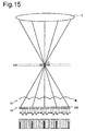
- FIGS. 14 to 16 show examples of the weighting coefficient for obtaining the pixel value L(5) of the virtual pixel located at the coordinate x 5 .
- the designated aperture value by the user is minimum.
- the five pixels a, b, c, d, and e arrayed in one direction are selected.
- a length of a bar corresponding to each pixel represents a value (a relative value) of a weighting coefficient applied to the output value of each pixel. An optimum weighting value may be experimentally obtained.
- values of weighting coefficients w1, w2, w3, w4, and w5 respectively correspond to lengths of bars shown in FIGS. 14 and 15 . Since the examples shown in FIGS. 14 and 15 assume the case where the designated aperture value by the user is minimum (maximum aperture size), if the designated aperture value by the user is the medium value (medium aperture size), the coefficients w1 and w5 of the weighting coefficients w1, w2, w3, w4, and w5 are set to extremely small values.
- the coefficients w1, w2, w4, and w5 of the weighting coefficients w1, w2, w3, w4, and w5 are set to extremely small values.
- an output value vector of the output values of all pixels of the image sensor 13 is multiplied by a weighting coefficient matrix, thereby forming the synthetic image data of the designated image plane.
- the size of the output value vector in the vertical direction corresponds to the total number of pixels of the image sensor 13 .
- the size of the weighting coefficient matrix in the horizontal direction corresponds to the size of the output value vector in the vertical direction.
- the size of the weighting coefficient matrix in the vertical direction corresponds to the number of virtual pixels of the image data for synthesis.
- the content of the weighting coefficient matrix is determined in accordance with the height Z of the designated image plane by the user, and the designated aperture value by the user. This determination is properly executed by the arithmetic processing circuit 15 .
- weighting coefficient matrices may be previously stored in the memory 16 (see FIG. 16 ).
- the arithmetic processing circuit 15 may select one of the weighting coefficient matrices in accordance with the designated image plane and the designated aperture value by the user.
- the resolution of the image data may be designated by the user.
- the resolution may be designated through the user interface 18 in a manner similar to the designation of the image plane and the aperture value.
- the setting of the resolution of the image data may be performed such that the arithmetic processing circuit 15 interpolates or sub-samples (or skips) the output values of the pixel array 130 (and/or pixel values of virtual pixels of image data), if needed.
- an efficient way of creating the entire image involves, after the position of the designated image plane (the distance from the microlens array plane) being determined, the image sizes of the pixel array located in the rear of the microlens being changed (increased as the distance is increased) in accordance with the position of the designated image plane, the image data sets related to the adjacent microlens being inverted, then the image data sets being mutually shifted by predetermined amounts, and the image data sets being added for synthesis.
- the weighting of the addition for synthesis is changed in accordance with the designated aperture value (aperture condition).
- This embodiment is an example of an image synthesis method for increasing the resolution of the image data. Note that this synthesis method may be applied only when the designated image plane is located in the vicinity of the front end of the synthesis range L (Z ⁇ L).
- pixel interpolation is performed in the pixel array 130 .
- Obtaining the pixel value of the virtual pixel with the width ⁇ at the position located at the distance L from the microlens ML means obtaining a light amount at an intermediate position of an image which is formed by projecting the pixel of the pixel array 130 through the microlens ML toward the photographic lens 11 (imaging optical system).
- imaging optical system imaging optical system
- an envelope function (solid line) of the pixel values is obtained through the interpolation, window functions (x, y, z, ⁇ , ⁇ ) (broken line) corresponding to ⁇ are used, and accordingly, the pixel values of the virtual pixels are obtained as the sum of products of both functions (the envelope function and the window functions).
- the bar graph shown at the right portion of the FIG. 17( a ) represents a distribution of output values of the five pixels arrayed in the pixel array 130 .
- a smooth distribution as indicated by a curved line can be obtained.
- nine pixel values can be obtained, in a manner similar to a case where five or more pixels (hereinafter, assuming nine pixels) are arrayed in the pixel array 130 .
- the distribution curve W of the light amount distribution depends on the coordinates (X, Y, Z) of the virtual pixel, the width ⁇ of the virtual pixel, and the solid angle ⁇ of the emitted bundles of rays due to the image formation relationship between the virtual pixel and the pixel array 130 .
- the light amount of the bundles of rays emitted form the virtual pixel can be obtained.
- Such a weighted sum is obtained for bundles of rays emitted from the virtual pixels at various angles, and then the sum (or the weighted sum) of these values are obtained, thereby obtaining the pixel values of the virtual pixels. Further, this calculation is performed for all virtual pixels of the designated image plane, so that synthetic image data of the designated image plane can be formed with the resolution ⁇ .
- the data which is the basis of the calculation is similar to that of the first embodiment (i.e., the data is the pixel outputs of all pixels of the image sensor 13 ). Therefore, since the weighting coefficient matrix is determined on the basis of the synthesis method, in a manner similar to the first embodiment, image data of the designated image plane can be collectively obtained merely by multiplying the output vector with the weighting coefficient matrix.
- the size in the vertical direction of the weighting coefficient matrix is increased by an amount of the increased resolution (by an increase amount of the number of the virtual pixels).
- a third embodiment is described below.
- the image-capturing apparatus and the image synthesis method of the first embodiment are partly modified. Only the modified point is described here.
- Each pixel array 130 of the image sensor 13 of the image-capturing apparatus has a color filter array as shown in FIG. 18( a ).
- the color filter array includes filters R that transmit only a red-light component among visible light entering the pixels of the pixel array 130 , filters G that transmit only a green-light component, and filters B that transmit only a blue-color component, these filters R, G, B being arrayed in a Bayer pattern.
- the color filter array in this embodiment provides different spectral sensitivity characteristics for three colors, to the pixels.
- the Bayer pattern is a pattern in which the filters G are arranged on the pixels of the pixel array 130 in a checkered pattern, and the filters R and B are alternately arranged on the residual pixels.
- the pixel provided with the filter G is referred to as a “G pixel”
- the pixel provided with the filter R is referred to as an “R pixel”
- the pixel provided with the filter B is referred to as a “B pixel”.
- pixel interpolation is performed by a known interpolation method.
- pixel outputs of twelve G pixels are interpolated to obtain pixel values of twenty-five G pixels for the entire pixel array 130 .
- pixel outputs of six R pixels are interpolated to obtain pixel values of twenty-five R pixels for the entire pixel array 130 .
- pixel outputs for six B pixels are interpolated to obtain pixel values of twenty-five B pixels for the entire pixel array 130 .
- the processing described in the above embodiment is applied to each surface, thereby providing a color image.
- the color filter array of this image-capturing apparatus uses the Bayer pattern, other pattern may be used.
- the filters G may be arranged in a striped pattern, and the filters R and B may be arranged alternately in columns between the columns of the filter G.
- a transfer portion or the like is disposed at a gap between the photoreceptors of the photoelectric conversion elements which define the pixels of the pixel array 130 , and hence, the gap does not become small. In this state, the bundle of rays entering the gap may be a loss. Therefore, in this image-capturing apparatus, as shown in FIG. 19( a ), microlenses ML′ having a diameter similar to the pixel pitch may be provided on the photoreceptors of the photoelectric conversion elements, so as to increase converging efficiency toward each pixel.
- the optical axis of the microlens in the second layer for defining the pixel may be preferably slightly shifted (deflected) toward the inner side from the center of the photoreceptor of the photoelectric conversion element, at the edges of the pixel array 130 . Accordingly, the converging efficiency to the edge pixel may become close to the converging efficiency to the center pixel.
- Each microlens of the second-layer microlens array is deflected with respect to its photoelectric conversion element in accordance with the positional relationship between the microlenses of the microlens array 12 and the microlenses of the second-layer microlens array. Therefore, the deflection amount increases as the position of the microlens ML′ comes away from the optical axis of the microlens ML.
- a field lens FL may be disposed directly in the front of the microlens array 12 . Disposing the field lens FL may control the angles of the bundles of rays incident on the microlens ML located at a high position of the image height thereof.
- the image sensor 13 in which the plurality of partitioned pixel arrays 130 are two-dimensionally arranged may be prepared, and necessary portions of the image sensor may be selectively used.
- the image-capturing apparatus may be provided with a display section such as a monitor.
- synthetic image data, information associated with the image data, and the like may be displayed on the display section.
- the designated image plane is one, the designated plane may be plural.
- the present invention features that a plurality of focal planes can be desirably provided after shooting. Since image data of the plurality of designated image planes represent three-dimensional image, the present invention can be used as a 3D image-capturing apparatus.
- a shooting point may be designated instead of the image plane.
- the image-capturing apparatus is only required to form synthetic luminance data at the shooting point (designated point).
- Items which may be designated by the user may include a “shooting range”.
- the image-capturing apparatus is only required to form synthetic image data within the designated shooting range.
- the whole processing related to the image synthesis is executed by the arithmetic processing circuit 15
- apart of or the entire processing may be executed by an external computer of the image-capturing apparatus.
- a program for image synthesis is previously installed in the computer.
- the image-capturing apparatus having the above-mentioned configuration may capture an image, transfer the captured image to a personal computer, and the personal computer may execute the whole processing.
- FIG. 22 is an illustration showing a configuration for processing with a personal computer 101 .
- the personal computer 101 is connected to a digital camera 102 as the above-described image-capturing apparatus, and acquires image data captured by the digital camera 102 .
- the image data captured by the digital camera 102 may be acquired using a recording medium 103 , such as a CD-ROM, or other computer 104 .
- the personal computer 101 is connected to the computer 104 through the Internet or other electric telecommunication line 105 .
- a program executed by the personal computer 101 is provided by a recording medium such as a CD-ROM, or by other computer through the Internet, or other electric telecommunication line, and is installed in the personal computer 101 , in a manner similar to the configuration shown in FIG. 21 .
- the personal computer 101 has a CPU (not shown) and a peripheral circuit (not shown). The CPU executes the installed program.
- the program is converted into a signal on a carrier wave that carries the signal through a transmission medium, i.e., the electric telecommunication line.
- the program is supplied as a computer program product in various forms of, for example, a recording medium and a carrier wave, to be readable by the computer.
- FIG. 23 is a flowchart showing the processing of the program executed by the personal computer 101 .
- step S 1 image data is acquired (obtained) from the digital camera 102 .
- the image data acquired from the digital camera 102 is image data composed of outputs of all pixels of the image sensor 13 .
- an image plane which was designated by the user using an input device such as a monitor or a keyboard of the personal computer 101 , is acquired.
- a designated aperture value is acquired in a similar manner.
- step S 4 synthesis processing is performed on the basis of the image data acquired in step S 1 , and the designated image plane as well as the designated aperture value.
- the personal computer 101 performs the synthesis processing, which is executed by the arithmetic processing circuit 15 in the above-described embodiment, using a software.
- step S 5 the synthetic image data is stored in hard disk (not shown), or the like. With the above procedure, the personal computer can provide an image focused at a desired distance after shooting by using data obtained by one shooting.
Abstract
Description
L/g=E/Pd (i)
L=g*P/Pd (ii)
1/L+1/g=1/fm (iii)
A≈L/D (1)
Fa≈L/A≈D (2)
Fa≈D (3)
Fa>10 (4)
D>10 μm (5)
D>20 μm (6)
-
- the number of pixels n in one direction of the
pixel array 130=5 - the array pitch P of the microlens ML=15 μm,
- the number of pixels n in one direction of the
-
- the synthesis range L=n×F=300 μm, and
L(5)=Out(a 5)+Out(b 5)+Out(c 5)+Out(d 5)+Out(e 5) (1)
L(6)=Out(a 6)+Out(b 6)+Out(c 6)+Out(d 6)+Out(e 6) (1′)
L(i)=Out(a i)+Out(b i)+Out(c i)+Out(d i)+Out(e i) (1″)
L(i)=Out(c i) (2)
L(i)=Out(b i)+Out(c i)+Out(d i) (3)
L(5)=Out(a 3)+Out(b 4)+Out(c 5)+Out(d 6)+Out(e 7) (4)
L(6)=Out(a 4)+Out(b 5)+Out(c 6)+Out(d 7)+Out(e 8) (4′)
L(i)=Out(a i−2)+Out(b i−1)+Out(c i)+Out(d i−1)+Out(e i+2) (4″)
L(i)=Out(c i) (5)
L(i)=Out(b i−1)+Out(c i)+Out(d i+1) (6)
Out(a3)×q1+Out(b3)×q2 (7)
Claims (9)
Applications Claiming Priority (3)
| Application Number | Priority Date | Filing Date | Title |
|---|---|---|---|
| JP2005183729A JP4826152B2 (en) | 2005-06-23 | 2005-06-23 | Image composition method and imaging apparatus |
| JP2005-183729 | 2005-06-23 | ||
| PCT/JP2006/312505 WO2006137481A1 (en) | 2005-06-23 | 2006-06-22 | Image input device, photo-detection device, image synthesis method |
Publications (2)
| Publication Number | Publication Date |
|---|---|
| US20090140131A1 US20090140131A1 (en) | 2009-06-04 |
| US7732744B2 true US7732744B2 (en) | 2010-06-08 |
Family
ID=37570508
Family Applications (1)
| Application Number | Title | Priority Date | Filing Date |
|---|---|---|---|
| US11/993,758 Active 2026-12-31 US7732744B2 (en) | 2005-06-23 | 2006-06-22 | Image input apparatus, photodetection apparatus, and image synthesis method |
Country Status (3)
| Country | Link |
|---|---|
| US (1) | US7732744B2 (en) |
| JP (1) | JP4826152B2 (en) |
| WO (1) | WO2006137481A1 (en) |
Cited By (51)
| Publication number | Priority date | Publication date | Assignee | Title |
|---|---|---|---|---|
| US20090041448A1 (en) * | 2007-08-06 | 2009-02-12 | Georgiev Todor G | Method and Apparatus for Radiance Capture by Multiplexing in the Frequency Domain |
| US20090102956A1 (en) * | 2007-10-18 | 2009-04-23 | Georgiev Todor G | Fast Computational Camera Based On Two Arrays of Lenses |
| US20090122175A1 (en) * | 2005-03-24 | 2009-05-14 | Michihiro Yamagata | Imaging device and lens array used therein |
| US20090268970A1 (en) * | 2008-04-29 | 2009-10-29 | Sevket Derin Babacan | Method and Apparatus for Block-Based Compression of Light-field Images |
| US20090295829A1 (en) * | 2008-01-23 | 2009-12-03 | Georgiev Todor G | Methods and Apparatus for Full-Resolution Light-Field Capture and Rendering |
| US20100020187A1 (en) * | 2006-04-04 | 2010-01-28 | Georgiev Todor G | Plenoptic camera |
| US20100045844A1 (en) * | 2008-08-21 | 2010-02-25 | Sony Corporation | Image pickup apparatus, display and image processing apparatus |
| US20100128152A1 (en) * | 2008-11-21 | 2010-05-27 | Sony Corporation | Image pickup apparatus |
| US20100215354A1 (en) * | 2009-02-24 | 2010-08-26 | Nikon Corporation | Imaging apparatus and image synthesis method |
| US20110076004A1 (en) * | 2009-09-29 | 2011-03-31 | Raytheon Company | Anamorphic focal array |
| US7962033B2 (en) | 2008-01-23 | 2011-06-14 | Adobe Systems Incorporated | Methods and apparatus for full-resolution light-field capture and rendering |
| US20110205388A1 (en) * | 2008-11-07 | 2011-08-25 | Nikon Corporation | Image-capturing device and image processing method |
| US8189089B1 (en) | 2009-01-20 | 2012-05-29 | Adobe Systems Incorporated | Methods and apparatus for reducing plenoptic camera artifacts |
| US20120147247A1 (en) * | 2010-12-14 | 2012-06-14 | Samsung Electronics Co., Ltd. | Optical system and imaging apparatus including the same |
| US8228417B1 (en) | 2009-07-15 | 2012-07-24 | Adobe Systems Incorporated | Focused plenoptic camera employing different apertures or filtering at different microlenses |
| US20120188422A1 (en) * | 2011-01-20 | 2012-07-26 | Kwang-Bo Cho | Imaging system with an array of image sensors |
| US8244058B1 (en) | 2008-05-30 | 2012-08-14 | Adobe Systems Incorporated | Method and apparatus for managing artifacts in frequency domain processing of light-field images |
| US8290358B1 (en) * | 2007-06-25 | 2012-10-16 | Adobe Systems Incorporated | Methods and apparatus for light-field imaging |
| US8315476B1 (en) | 2009-01-20 | 2012-11-20 | Adobe Systems Incorporated | Super-resolution with the focused plenoptic camera |
| US20120300091A1 (en) * | 2011-05-23 | 2012-11-29 | Shroff Sapna A | Focusing and Focus Metrics for a Plenoptic Imaging System |
| US8345144B1 (en) | 2009-07-15 | 2013-01-01 | Adobe Systems Incorporated | Methods and apparatus for rich image capture with focused plenoptic cameras |
| US8358366B1 (en) | 2010-05-28 | 2013-01-22 | Adobe Systems Incorporate | Methods and apparatus for high-speed digital imaging |
| US8542312B2 (en) | 2011-03-31 | 2013-09-24 | Casio Computer Co., Ltd. | Device having image reconstructing function, method, and storage medium |
| US20130335547A1 (en) * | 2012-06-14 | 2013-12-19 | Canon Kabushiki Kaisha | Signal processing apparatus for focus detection, signal processing method, and image pickup apparatus |
| US20140028869A1 (en) * | 2011-09-12 | 2014-01-30 | Canon Kabushiki Kaisha | Image processing method, image processing apparatus and image pickup apparatus |
| US8665341B2 (en) | 2010-08-27 | 2014-03-04 | Adobe Systems Incorporated | Methods and apparatus for rendering output images with simulated artistic effects from focused plenoptic camera data |
| US8711269B2 (en) * | 2010-12-17 | 2014-04-29 | Canon Kabushiki Kaisha | Image sensing apparatus and method of controlling the image sensing apparatus |
| US8724000B2 (en) | 2010-08-27 | 2014-05-13 | Adobe Systems Incorporated | Methods and apparatus for super-resolution in integral photography |
| US8749694B2 (en) | 2010-08-27 | 2014-06-10 | Adobe Systems Incorporated | Methods and apparatus for rendering focused plenoptic camera data using super-resolved demosaicing |
| US8803990B2 (en) | 2011-01-25 | 2014-08-12 | Aptina Imaging Corporation | Imaging system with multiple sensors for producing high-dynamic-range images |
| US8803918B2 (en) | 2010-08-27 | 2014-08-12 | Adobe Systems Incorporated | Methods and apparatus for calibrating focused plenoptic camera data |
| US8817015B2 (en) | 2010-03-03 | 2014-08-26 | Adobe Systems Incorporated | Methods, apparatus, and computer-readable storage media for depth-based rendering of focused plenoptic camera data |
| US20140293117A1 (en) * | 2011-12-02 | 2014-10-02 | Canon Kabushiki Kaisha | Image processing apparatus and image processing method |
| US8854724B2 (en) | 2012-03-27 | 2014-10-07 | Ostendo Technologies, Inc. | Spatio-temporal directional light modulator |
| US8928969B2 (en) | 2011-12-06 | 2015-01-06 | Ostendo Technologies, Inc. | Spatio-optical directional light modulator |
| US8947585B2 (en) | 2012-03-21 | 2015-02-03 | Casio Computer Co., Ltd. | Image capturing apparatus, image processing method, and storage medium |
| US9019424B2 (en) | 2011-07-25 | 2015-04-28 | Canon Kabushiki Kaisha | Image pickup apparatus, control method thereof, and program |
| US9030550B2 (en) | 2011-03-25 | 2015-05-12 | Adobe Systems Incorporated | Thin plenoptic cameras using solid immersion lenses |
| US9124828B1 (en) * | 2013-09-19 | 2015-09-01 | The United States Of America As Represented By The Secretary Of The Navy | Apparatus and methods using a fly's eye lens system for the production of high dynamic range images |
| US9131130B2 (en) | 2011-12-19 | 2015-09-08 | Canon Kabushiki Kaisha | Image pickup apparatus, and control method thereof |
| US9137441B2 (en) | 2012-02-16 | 2015-09-15 | Ricoh Co., Ltd. | Spatial reconstruction of plenoptic images |
| US9179126B2 (en) | 2012-06-01 | 2015-11-03 | Ostendo Technologies, Inc. | Spatio-temporal light field cameras |
| US9438778B2 (en) | 2014-08-08 | 2016-09-06 | Industrial Technology Research Institute | Image pickup device and light field image pickup lens |
| US9451148B2 (en) | 2012-06-15 | 2016-09-20 | Canon Kabushiki Kaisha | Image recording apparatus and image reproducing apparatus |
| US9538075B2 (en) | 2013-12-30 | 2017-01-03 | Indiana University Research And Technology Corporation | Frequency domain processing techniques for plenoptic images |
| US9791599B2 (en) | 2014-03-24 | 2017-10-17 | Kabushiki Kaisha Toshiba | Image processing method and imaging device |
| US10009533B2 (en) | 2011-07-25 | 2018-06-26 | Canon Kabushiki Kaisha | Image pickup apparatus and control method thereof with contrast focus evaluation |
| US10092183B2 (en) | 2014-08-31 | 2018-10-09 | Dr. John Berestka | Systems and methods for analyzing the eye |
| US10334161B2 (en) | 2014-09-30 | 2019-06-25 | Canon Kabushiki Kaisha | Image processing apparatus, image processing method, computer program and imaging apparatus |
| US10587798B2 (en) | 2012-02-28 | 2020-03-10 | Nikon Corporation | Image processing apparatus |
| US20200400423A1 (en) * | 2017-12-27 | 2020-12-24 | Ams Sensors Singapore Pte. Ltd. | Optoelectronic modules and methods for operating the same |
Families Citing this family (227)
| Publication number | Priority date | Publication date | Assignee | Title |
|---|---|---|---|---|
| JP4645358B2 (en) * | 2004-08-20 | 2011-03-09 | ソニー株式会社 | Imaging apparatus and imaging method |
| JP4826152B2 (en) * | 2005-06-23 | 2011-11-30 | 株式会社ニコン | Image composition method and imaging apparatus |
| US10298834B2 (en) | 2006-12-01 | 2019-05-21 | Google Llc | Video refocusing |
| US20100265385A1 (en) * | 2009-04-18 | 2010-10-21 | Knight Timothy J | Light Field Camera Image, File and Configuration Data, and Methods of Using, Storing and Communicating Same |
| US8559705B2 (en) | 2006-12-01 | 2013-10-15 | Lytro, Inc. | Interactive refocusing of electronic images |
| JP4803676B2 (en) * | 2007-03-09 | 2011-10-26 | 株式会社リコー | Image input device and personal authentication device |
| JP5380782B2 (en) * | 2007-03-26 | 2014-01-08 | 株式会社ニコン | Imaging device |
| JP5179784B2 (en) * | 2007-06-07 | 2013-04-10 | 株式会社ユニバーサルエンターテインメント | Three-dimensional coordinate measuring apparatus and program executed in three-dimensional coordinate measuring apparatus |
| DE102007031230B3 (en) * | 2007-07-04 | 2008-10-30 | Bundesdruckerei Gmbh | Document capture system and document capture process |
| JP4968527B2 (en) * | 2007-07-10 | 2012-07-04 | ソニー株式会社 | Imaging device |
| JP5115068B2 (en) * | 2007-07-13 | 2013-01-09 | ソニー株式会社 | Imaging device |
| JP4967873B2 (en) * | 2007-07-13 | 2012-07-04 | ソニー株式会社 | Imaging device |
| US20090122148A1 (en) * | 2007-09-14 | 2009-05-14 | Fife Keith G | Disjoint light sensing arrangements and methods therefor |
| WO2009044776A1 (en) | 2007-10-02 | 2009-04-09 | Nikon Corporation | Light receiving device, focal point detecting device and imaging device |
| JP4905326B2 (en) * | 2007-11-12 | 2012-03-28 | ソニー株式会社 | Imaging device |
| JP5224124B2 (en) * | 2007-12-12 | 2013-07-03 | ソニー株式会社 | Imaging device |
| JP5067154B2 (en) * | 2007-12-27 | 2012-11-07 | ソニー株式会社 | Imaging device |
| JP4941332B2 (en) | 2008-01-28 | 2012-05-30 | ソニー株式会社 | Imaging device |
| JP5130178B2 (en) * | 2008-03-17 | 2013-01-30 | 株式会社リコー | Focal length detection apparatus, imaging apparatus, imaging method, and camera |
| US8866920B2 (en) | 2008-05-20 | 2014-10-21 | Pelican Imaging Corporation | Capturing and processing of images using monolithic camera array with heterogeneous imagers |
| US8902321B2 (en) | 2008-05-20 | 2014-12-02 | Pelican Imaging Corporation | Capturing and processing of images using monolithic camera array with heterogeneous imagers |
| US11792538B2 (en) | 2008-05-20 | 2023-10-17 | Adeia Imaging Llc | Capturing and processing of images including occlusions focused on an image sensor by a lens stack array |
| JP5229541B2 (en) * | 2008-05-29 | 2013-07-03 | 株式会社ニコン | Distance measuring device, distance measuring method, and program |
| KR101483714B1 (en) * | 2008-06-18 | 2015-01-16 | 삼성전자 주식회사 | Apparatus and method for capturing digital image |
| JP5256933B2 (en) * | 2008-08-25 | 2013-08-07 | 株式会社ニコン | Focus information detector |
| JP2010057067A (en) * | 2008-08-29 | 2010-03-11 | Sony Corp | Image pickup apparatus and image processing apparatus |
| JP5369564B2 (en) * | 2008-09-11 | 2013-12-18 | 株式会社ニコン | Shape measuring device |
| JP5369563B2 (en) * | 2008-09-11 | 2013-12-18 | 株式会社ニコン | Shape measuring device |
| KR101441586B1 (en) * | 2008-10-06 | 2014-09-23 | 삼성전자 주식회사 | Apparatus and method for capturing image |
| JP5245716B2 (en) * | 2008-10-27 | 2013-07-24 | 株式会社ニコン | Camera lens adapter and camera system |
| JP2010109921A (en) * | 2008-10-31 | 2010-05-13 | Nikon Corp | Image synthesizing apparatus |
| WO2010065344A1 (en) | 2008-11-25 | 2010-06-10 | Refocus Imaging, Inc. | System of and method for video refocusing |
| WO2010077625A1 (en) | 2008-12-08 | 2010-07-08 | Refocus Imaging, Inc. | Light field data acquisition devices, and methods of using and manufacturing same |
| US7949252B1 (en) | 2008-12-11 | 2011-05-24 | Adobe Systems Incorporated | Plenoptic camera with large depth of field |
| US9432591B2 (en) | 2009-01-05 | 2016-08-30 | Duke University | Multiscale optical system having dynamic camera settings |
| US9494771B2 (en) | 2009-01-05 | 2016-11-15 | Duke University | Quasi-monocentric-lens-based multi-scale optical system |
| US9395617B2 (en) | 2009-01-05 | 2016-07-19 | Applied Quantum Technologies, Inc. | Panoramic multi-scale imager and method therefor |
| US8259212B2 (en) * | 2009-01-05 | 2012-09-04 | Applied Quantum Technologies, Inc. | Multiscale optical system |
| US9635253B2 (en) | 2009-01-05 | 2017-04-25 | Duke University | Multiscale telescopic imaging system |
| US10725280B2 (en) | 2009-01-05 | 2020-07-28 | Duke University | Multiscale telescopic imaging system |
| US8570427B2 (en) | 2009-01-28 | 2013-10-29 | Nikon Corporation | Image-capturing device having focus adjustment function, image creation method including focus adjustment function, and program product for image-capturing device having focus adjustment function |
| JP4692654B2 (en) * | 2009-02-20 | 2011-06-01 | 株式会社ニコン | Imaging apparatus and image processing program |
| JP4710983B2 (en) * | 2009-01-28 | 2011-06-29 | 株式会社ニコン | Image composition device, imaging device, and image composition method |
| JP5446311B2 (en) * | 2009-02-20 | 2014-03-19 | 株式会社ニコン | Imaging device |
| JP4766133B2 (en) | 2009-03-11 | 2011-09-07 | 株式会社ニコン | Imaging device |
| DE102009013112A1 (en) * | 2009-03-13 | 2010-09-16 | Fraunhofer-Gesellschaft zur Förderung der angewandten Forschung e.V. | Method for producing a multiplicity of microoptoelectronic components and microoptoelectronic component |
| US8908058B2 (en) * | 2009-04-18 | 2014-12-09 | Lytro, Inc. | Storage and transmission of pictures including multiple frames |
| JP5394814B2 (en) * | 2009-05-01 | 2014-01-22 | 三星電子株式会社 | Photodetection element and imaging device |
| JP5515396B2 (en) * | 2009-05-08 | 2014-06-11 | ソニー株式会社 | Imaging device |
| JP4952768B2 (en) | 2009-10-27 | 2012-06-13 | 株式会社ニコン | Imaging apparatus and image analysis computer program |
| JP5434503B2 (en) * | 2009-11-16 | 2014-03-05 | 株式会社ニコン | Image composition device and imaging device |
| EP2502115A4 (en) | 2009-11-20 | 2013-11-06 | Pelican Imaging Corp | Capturing and processing of images using monolithic camera array with heterogeneous imagers |
| JP5526733B2 (en) * | 2009-11-25 | 2014-06-18 | 株式会社ニコン | Image composition device, image reproduction device, and imaging device |
| US8400555B1 (en) | 2009-12-01 | 2013-03-19 | Adobe Systems Incorporated | Focused plenoptic camera employing microlenses with different focal lengths |
| JP5490514B2 (en) * | 2009-12-22 | 2014-05-14 | 三星電子株式会社 | Imaging apparatus and imaging method |
| JP5273033B2 (en) * | 2009-12-25 | 2013-08-28 | 株式会社ニコン | Imaging apparatus and image reproduction apparatus |
| JP5970816B2 (en) * | 2009-12-28 | 2016-08-17 | 株式会社ニコン | Image processing apparatus, imaging device, and imaging apparatus |
| US8749620B1 (en) | 2010-02-20 | 2014-06-10 | Lytro, Inc. | 3D light field cameras, images and files, and methods of using, operating, processing and viewing same |
| JP5499778B2 (en) | 2010-03-03 | 2014-05-21 | 株式会社ニコン | Imaging device |
| JP5881679B2 (en) | 2010-04-27 | 2016-03-09 | デューク ユニバーシティ | Multi-scale optical system based on a lens group with a single center and its use |
| KR101824672B1 (en) | 2010-05-12 | 2018-02-05 | 포토네이션 케이맨 리미티드 | Architectures for imager arrays and array cameras |
| JP5671842B2 (en) * | 2010-06-03 | 2015-02-18 | 株式会社ニコン | Image processing apparatus and imaging apparatus |
| JP5488221B2 (en) * | 2010-06-09 | 2014-05-14 | 株式会社ニコン | Imaging device |
| JP2016001326A (en) * | 2010-06-16 | 2016-01-07 | 株式会社ニコン | Image display device |
| JP6149339B2 (en) | 2010-06-16 | 2017-06-21 | 株式会社ニコン | Display device |
| SE535491C2 (en) * | 2010-06-21 | 2012-08-28 | Rolling Optics Ab | Method and apparatus for reading optical devices |
| JP5423893B2 (en) * | 2010-06-28 | 2014-02-19 | 株式会社ニコン | Imaging apparatus, image processing apparatus, and image processing program recording medium |
| DE102010031535A1 (en) * | 2010-07-19 | 2012-01-19 | Fraunhofer-Gesellschaft zur Förderung der angewandten Forschung e.V. | An image pickup device and method for picking up an image |
| US20140192238A1 (en) | 2010-10-24 | 2014-07-10 | Linx Computational Imaging Ltd. | System and Method for Imaging and Image Processing |
| JP5549545B2 (en) * | 2010-11-02 | 2014-07-16 | 株式会社ニコン | projector |
| EP2642260A4 (en) * | 2010-11-16 | 2015-12-09 | Nikon Corp | Multiband camera, and multiband image capturing method |
| JP2012129713A (en) * | 2010-12-14 | 2012-07-05 | Samsung Electronics Co Ltd | Optical system and imaging apparatus provided with the same |
| US8878950B2 (en) | 2010-12-14 | 2014-11-04 | Pelican Imaging Corporation | Systems and methods for synthesizing high resolution images using super-resolution processes |
| JP5699609B2 (en) | 2011-01-06 | 2015-04-15 | ソニー株式会社 | Image processing apparatus and image processing method |
| WO2012096153A1 (en) * | 2011-01-12 | 2012-07-19 | 株式会社ニコン | Microscope system |
| JP5263310B2 (en) * | 2011-01-31 | 2013-08-14 | 株式会社ニコン | Image generation apparatus, imaging apparatus, and image generation method |
| US8768102B1 (en) | 2011-02-09 | 2014-07-01 | Lytro, Inc. | Downsampling light field images |
| JP5716465B2 (en) * | 2011-03-09 | 2015-05-13 | ソニー株式会社 | Imaging device |
| JP2012191351A (en) * | 2011-03-09 | 2012-10-04 | Sony Corp | Image pickup apparatus and image processing method |
| JP5623313B2 (en) * | 2011-03-10 | 2014-11-12 | キヤノン株式会社 | Imaging apparatus and imaging optical system |
| JP2014519741A (en) | 2011-05-11 | 2014-08-14 | ペリカン イメージング コーポレイション | System and method for transmitting and receiving array camera image data |
| JP5984493B2 (en) * | 2011-06-24 | 2016-09-06 | キヤノン株式会社 | Image processing apparatus, image processing method, imaging apparatus, and program |
| US20130265459A1 (en) | 2011-06-28 | 2013-10-10 | Pelican Imaging Corporation | Optical arrangements for use with an array camera |
| JP5743769B2 (en) * | 2011-07-15 | 2015-07-01 | キヤノン株式会社 | Image processing apparatus and image processing method |
| US9184199B2 (en) | 2011-08-01 | 2015-11-10 | Lytro, Inc. | Optical assembly including plenoptic microlens array |
| JP5618943B2 (en) * | 2011-08-19 | 2014-11-05 | キヤノン株式会社 | Image processing method, imaging apparatus, image processing apparatus, and image processing program |
| JP2013064996A (en) * | 2011-08-26 | 2013-04-11 | Nikon Corp | Three-dimensional image display device |
| JP5623356B2 (en) * | 2011-08-29 | 2014-11-12 | キヤノン株式会社 | Imaging device |
| WO2013043761A1 (en) | 2011-09-19 | 2013-03-28 | Pelican Imaging Corporation | Determining depth from multiple views of a scene that include aliasing using hypothesized fusion |
| EP2761534B1 (en) | 2011-09-28 | 2020-11-18 | FotoNation Limited | Systems for encoding light field image files |
| JP2013081087A (en) * | 2011-10-04 | 2013-05-02 | Sony Corp | Imaging device |
| US8941750B2 (en) * | 2011-12-27 | 2015-01-27 | Casio Computer Co., Ltd. | Image processing device for generating reconstruction image, image generating method, and storage medium |
| JP5354005B2 (en) * | 2011-12-27 | 2013-11-27 | カシオ計算機株式会社 | Image processing apparatus, image processing method, and program |
| JP5360190B2 (en) * | 2011-12-27 | 2013-12-04 | カシオ計算機株式会社 | Image processing apparatus, image processing method, and program |
| JP5942428B2 (en) * | 2011-12-28 | 2016-06-29 | カシオ計算機株式会社 | Reconstructed image generating apparatus, reconstructed image generating method, and program |
| JP5818697B2 (en) | 2012-01-13 | 2015-11-18 | キヤノン株式会社 | Image generation method, imaging device, display device, program, and storage medium |
| US9412206B2 (en) | 2012-02-21 | 2016-08-09 | Pelican Imaging Corporation | Systems and methods for the manipulation of captured light field image data |
| US9554115B2 (en) * | 2012-02-27 | 2017-01-24 | Semiconductor Components Industries, Llc | Imaging pixels with depth sensing capabilities |
| US8811769B1 (en) | 2012-02-28 | 2014-08-19 | Lytro, Inc. | Extended depth of field and variable center of perspective in light-field processing |
| US8831377B2 (en) | 2012-02-28 | 2014-09-09 | Lytro, Inc. | Compensating for variation in microlens position during light-field image processing |
| US8948545B2 (en) | 2012-02-28 | 2015-02-03 | Lytro, Inc. | Compensating for sensor saturation and microlens modulation during light-field image processing |
| US8995785B2 (en) | 2012-02-28 | 2015-03-31 | Lytro, Inc. | Light-field processing and analysis, camera control, and user interfaces and interaction on light-field capture devices |
| US9420276B2 (en) | 2012-02-28 | 2016-08-16 | Lytro, Inc. | Calibration of light-field camera geometry via robust fitting |
| JP5882789B2 (en) * | 2012-03-01 | 2016-03-09 | キヤノン株式会社 | Image processing apparatus, image processing method, and program |
| JP6131545B2 (en) * | 2012-03-16 | 2017-05-24 | 株式会社ニコン | Image processing apparatus, imaging apparatus, and image processing program |
| JP2013214254A (en) * | 2012-04-04 | 2013-10-17 | Nikon Corp | Information detection device |
| JP5947602B2 (en) | 2012-04-11 | 2016-07-06 | キヤノン株式会社 | Imaging device |
| JP6089440B2 (en) * | 2012-04-26 | 2017-03-08 | 株式会社ニコン | Imaging device and imaging apparatus |
| US9210392B2 (en) | 2012-05-01 | 2015-12-08 | Pelican Imaging Coporation | Camera modules patterned with pi filter groups |
| JP5677366B2 (en) * | 2012-05-21 | 2015-02-25 | キヤノン株式会社 | Imaging device |
| JP6046922B2 (en) * | 2012-06-07 | 2016-12-21 | キヤノン株式会社 | FOCUS DETECTION DEVICE, IMAGING DEVICE, CONTROL METHOD, PROGRAM, AND RECORDING MEDIUM |
| JP5553862B2 (en) * | 2012-06-11 | 2014-07-16 | キヤノン株式会社 | Image pickup apparatus and image pickup apparatus control method |
| JP5553863B2 (en) * | 2012-06-11 | 2014-07-16 | キヤノン株式会社 | Image processing method, imaging apparatus, image processing apparatus, and image processing program |
| JP5914192B2 (en) * | 2012-06-11 | 2016-05-11 | キヤノン株式会社 | Imaging apparatus and control method thereof |
| US10129524B2 (en) | 2012-06-26 | 2018-11-13 | Google Llc | Depth-assigned content for depth-enhanced virtual reality images |
| US9607424B2 (en) | 2012-06-26 | 2017-03-28 | Lytro, Inc. | Depth-assigned content for depth-enhanced pictures |
| US9858649B2 (en) | 2015-09-30 | 2018-01-02 | Lytro, Inc. | Depth-based image blurring |
| WO2014005123A1 (en) | 2012-06-28 | 2014-01-03 | Pelican Imaging Corporation | Systems and methods for detecting defective camera arrays, optic arrays, and sensors |
| US20140002674A1 (en) | 2012-06-30 | 2014-01-02 | Pelican Imaging Corporation | Systems and Methods for Manufacturing Camera Modules Using Active Alignment of Lens Stack Arrays and Sensors |
| JP5631935B2 (en) | 2012-07-11 | 2014-11-26 | 株式会社東芝 | Image processing apparatus, image processing method and program, and imaging apparatus |
| JP6344236B2 (en) | 2012-07-12 | 2018-06-20 | 株式会社ニコン | Image processing apparatus and imaging apparatus |
| JP6188290B2 (en) * | 2012-08-03 | 2017-08-30 | キヤノン株式会社 | Ranging device, imaging device, focus evaluation method, program, and storage medium |
| JP6029380B2 (en) | 2012-08-14 | 2016-11-24 | キヤノン株式会社 | Image processing apparatus, imaging apparatus including image processing apparatus, image processing method, and program |
| CN107346061B (en) | 2012-08-21 | 2020-04-24 | 快图有限公司 | System and method for parallax detection and correction in images captured using an array camera |
| WO2014032020A2 (en) | 2012-08-23 | 2014-02-27 | Pelican Imaging Corporation | Feature based high resolution motion estimation from low resolution images captured using an array source |
| JP5988790B2 (en) * | 2012-09-12 | 2016-09-07 | キヤノン株式会社 | Image processing apparatus, imaging apparatus, image processing method, and image processing program |
| US9214013B2 (en) | 2012-09-14 | 2015-12-15 | Pelican Imaging Corporation | Systems and methods for correcting user identified artifacts in light field images |
| US20140077324A1 (en) * | 2012-09-20 | 2014-03-20 | Sony Corporation | Solid-state image pickup device, method of manufacturing solid-state image pickup device, and electronic apparatus |
| EP2903258B1 (en) * | 2012-09-25 | 2018-04-25 | Fujifilm Corporation | Image-processing device and method, and image pickup device |
| CN104685860A (en) | 2012-09-28 | 2015-06-03 | 派力肯影像公司 | Generating images from light fields utilizing virtual viewpoints |
| JP6082223B2 (en) * | 2012-10-15 | 2017-02-15 | キヤノン株式会社 | Imaging apparatus, control method thereof, and program |
| US8997021B2 (en) | 2012-11-06 | 2015-03-31 | Lytro, Inc. | Parallax and/or three-dimensional effects for thumbnail image displays |
| US9143711B2 (en) | 2012-11-13 | 2015-09-22 | Pelican Imaging Corporation | Systems and methods for array camera focal plane control |
| US9667846B2 (en) * | 2012-11-27 | 2017-05-30 | Nokia Technologies Oy | Plenoptic camera apparatus, a method and a computer program |
| US9001226B1 (en) | 2012-12-04 | 2015-04-07 | Lytro, Inc. | Capturing and relighting images using multiple devices |
| TW201426018A (en) * | 2012-12-19 | 2014-07-01 | Ind Tech Res Inst | Image processing apparatus and image refocusing method |
| JP6198395B2 (en) * | 2013-01-08 | 2017-09-20 | キヤノン株式会社 | Imaging apparatus and control method thereof |
| US9565996B2 (en) * | 2013-01-18 | 2017-02-14 | Ricoh Company, Ltd. | Plenoptic otoscope |
| US10327627B2 (en) | 2013-01-18 | 2019-06-25 | Ricoh Company, Ltd. | Use of plenoptic otoscope data for aiding medical diagnosis |
| KR20140094395A (en) * | 2013-01-22 | 2014-07-30 | 삼성전자주식회사 | photographing device for taking a picture by a plurality of microlenses and method thereof |
| JP6055332B2 (en) * | 2013-02-12 | 2016-12-27 | キヤノン株式会社 | Image processing apparatus, imaging apparatus, control method, and program |
| US9462164B2 (en) | 2013-02-21 | 2016-10-04 | Pelican Imaging Corporation | Systems and methods for generating compressed light field representation data using captured light fields, array geometry, and parallax information |
| US9253380B2 (en) * | 2013-02-24 | 2016-02-02 | Pelican Imaging Corporation | Thin form factor computational array cameras and modular array cameras |
| US9774789B2 (en) | 2013-03-08 | 2017-09-26 | Fotonation Cayman Limited | Systems and methods for high dynamic range imaging using array cameras |
| US8866912B2 (en) | 2013-03-10 | 2014-10-21 | Pelican Imaging Corporation | System and methods for calibration of an array camera using a single captured image |
| US9888194B2 (en) | 2013-03-13 | 2018-02-06 | Fotonation Cayman Limited | Array camera architecture implementing quantum film image sensors |
| WO2014165244A1 (en) | 2013-03-13 | 2014-10-09 | Pelican Imaging Corporation | Systems and methods for synthesizing images from image data captured by an array camera using restricted depth of field depth maps in which depth estimation precision varies |
| WO2014164550A2 (en) | 2013-03-13 | 2014-10-09 | Pelican Imaging Corporation | System and methods for calibration of an array camera |
| US9106784B2 (en) | 2013-03-13 | 2015-08-11 | Pelican Imaging Corporation | Systems and methods for controlling aliasing in images captured by an array camera for use in super-resolution processing |
| WO2014153098A1 (en) | 2013-03-14 | 2014-09-25 | Pelican Imaging Corporation | Photmetric normalization in array cameras |
| US9578259B2 (en) | 2013-03-14 | 2017-02-21 | Fotonation Cayman Limited | Systems and methods for reducing motion blur in images or video in ultra low light with array cameras |
| WO2014145856A1 (en) | 2013-03-15 | 2014-09-18 | Pelican Imaging Corporation | Systems and methods for stereo imaging with camera arrays |
| US9445003B1 (en) | 2013-03-15 | 2016-09-13 | Pelican Imaging Corporation | Systems and methods for synthesizing high resolution images using image deconvolution based on motion and depth information |
| US9497429B2 (en) | 2013-03-15 | 2016-11-15 | Pelican Imaging Corporation | Extended color processing on pelican array cameras |
| US10122993B2 (en) | 2013-03-15 | 2018-11-06 | Fotonation Limited | Autofocus system for a conventional camera that uses depth information from an array camera |
| US9497370B2 (en) | 2013-03-15 | 2016-11-15 | Pelican Imaging Corporation | Array camera architecture implementing quantum dot color filters |
| US10334151B2 (en) | 2013-04-22 | 2019-06-25 | Google Llc | Phase detection autofocus using subaperture images |
| JP6221327B2 (en) * | 2013-04-26 | 2017-11-01 | 株式会社ニコン | Image sensor and camera |
| JP6239862B2 (en) * | 2013-05-20 | 2017-11-29 | キヤノン株式会社 | Focus adjustment apparatus, focus adjustment method and program, and imaging apparatus |
| KR102103983B1 (en) * | 2013-07-31 | 2020-04-23 | 삼성전자주식회사 | Light field image capturing apparatus including shifted microlens array |
| WO2015048694A2 (en) | 2013-09-27 | 2015-04-02 | Pelican Imaging Corporation | Systems and methods for depth-assisted perspective distortion correction |
| WO2015070105A1 (en) | 2013-11-07 | 2015-05-14 | Pelican Imaging Corporation | Methods of manufacturing array camera modules incorporating independently aligned lens stacks |
| US10119808B2 (en) | 2013-11-18 | 2018-11-06 | Fotonation Limited | Systems and methods for estimating depth from projected texture using camera arrays |
| EP3075140B1 (en) | 2013-11-26 | 2018-06-13 | FotoNation Cayman Limited | Array camera configurations incorporating multiple constituent array cameras |
| JP6476547B2 (en) * | 2014-01-28 | 2019-03-06 | 株式会社ニコン | Focus detection device and imaging device |
| JP6278728B2 (en) * | 2014-02-13 | 2018-02-14 | キヤノン株式会社 | Image processing apparatus, image generation apparatus, control method, and program |
| US10089740B2 (en) | 2014-03-07 | 2018-10-02 | Fotonation Limited | System and methods for depth regularization and semiautomatic interactive matting using RGB-D images |
| JP6581333B2 (en) | 2014-03-14 | 2019-09-25 | キヤノン株式会社 | Image processing apparatus, imaging apparatus, and program |
| US9305375B2 (en) | 2014-03-25 | 2016-04-05 | Lytro, Inc. | High-quality post-rendering depth blur |
| JP6360338B2 (en) | 2014-03-31 | 2018-07-18 | キヤノン株式会社 | Image processing apparatus, image processing method and program, and imaging apparatus |
| JP6506506B2 (en) | 2014-04-02 | 2019-04-24 | キヤノン株式会社 | Image processing apparatus, imaging apparatus, control method and program |
| JP2015198391A (en) | 2014-04-02 | 2015-11-09 | キヤノン株式会社 | Imaging apparatus, control method of imaging apparatus, and program |
| US9521319B2 (en) | 2014-06-18 | 2016-12-13 | Pelican Imaging Corporation | Array cameras and array camera modules including spectral filters disposed outside of a constituent image sensor |
| JP5721891B2 (en) * | 2014-08-01 | 2015-05-20 | キヤノン株式会社 | Imaging device |
| US9635332B2 (en) | 2014-09-08 | 2017-04-25 | Lytro, Inc. | Saturated pixel recovery in light-field images |
| CN113256730B (en) | 2014-09-29 | 2023-09-05 | 快图有限公司 | System and method for dynamic calibration of an array camera |
| JP6036799B2 (en) * | 2014-12-25 | 2016-11-30 | 株式会社ニコン | Image processing device |
| WO2016122404A1 (en) * | 2015-01-29 | 2016-08-04 | Heptagon Micro Optics Pte. Ltd. | Apparatus for producing patterned illumination |
| US10341632B2 (en) | 2015-04-15 | 2019-07-02 | Google Llc. | Spatial random access enabled video system with a three-dimensional viewing volume |
| US10440407B2 (en) | 2017-05-09 | 2019-10-08 | Google Llc | Adaptive control for immersive experience delivery |
| US10412373B2 (en) | 2015-04-15 | 2019-09-10 | Google Llc | Image capture for virtual reality displays |
| US10540818B2 (en) | 2015-04-15 | 2020-01-21 | Google Llc | Stereo image generation and interactive playback |
| US10567464B2 (en) | 2015-04-15 | 2020-02-18 | Google Llc | Video compression with adaptive view-dependent lighting removal |
| US10275898B1 (en) | 2015-04-15 | 2019-04-30 | Google Llc | Wedge-based light-field video capture |
| US10546424B2 (en) | 2015-04-15 | 2020-01-28 | Google Llc | Layered content delivery for virtual and augmented reality experiences |
| US10419737B2 (en) | 2015-04-15 | 2019-09-17 | Google Llc | Data structures and delivery methods for expediting virtual reality playback |
| US10444931B2 (en) | 2017-05-09 | 2019-10-15 | Google Llc | Vantage generation and interactive playback |
| US10565734B2 (en) | 2015-04-15 | 2020-02-18 | Google Llc | Video capture, processing, calibration, computational fiber artifact removal, and light-field pipeline |
| US11328446B2 (en) | 2015-04-15 | 2022-05-10 | Google Llc | Combining light-field data with active depth data for depth map generation |
| US10469873B2 (en) | 2015-04-15 | 2019-11-05 | Google Llc | Encoding and decoding virtual reality video |
| US9942474B2 (en) | 2015-04-17 | 2018-04-10 | Fotonation Cayman Limited | Systems and methods for performing high speed video capture and depth estimation using array cameras |
| EP3110130A1 (en) * | 2015-06-25 | 2016-12-28 | Thomson Licensing | Plenoptic camera and method of controlling the same |
| US9979909B2 (en) | 2015-07-24 | 2018-05-22 | Lytro, Inc. | Automatic lens flare detection and correction for light-field images |
| DE102015215844B4 (en) * | 2015-08-19 | 2017-05-18 | Fraunhofer-Gesellschaft zur Förderung der angewandten Forschung e.V. | A multi-aperture imaging apparatus, a portable apparatus, and a method of manufacturing a multi-aperture imaging apparatus |
| EP3144888A1 (en) * | 2015-09-17 | 2017-03-22 | Thomson Licensing | An apparatus and a method for generating data representing a pixel beam |
| JP6600217B2 (en) | 2015-09-30 | 2019-10-30 | キヤノン株式会社 | Image processing apparatus, image processing method, imaging apparatus, and control method thereof |
| CN106610521B (en) * | 2015-10-22 | 2019-11-19 | 中强光电股份有限公司 | Image-taking device and image shooting method |
| US10098529B2 (en) | 2015-10-28 | 2018-10-16 | Ricoh Company, Ltd. | Optical design of a light field otoscope |
| JP6028082B2 (en) * | 2015-11-02 | 2016-11-16 | オリンパス株式会社 | Imaging device |
| EP3182697A1 (en) * | 2015-12-15 | 2017-06-21 | Thomson Licensing | A method and apparatus for correcting vignetting effect caused on an image captured by lightfield cameras |
| WO2017150512A1 (en) * | 2016-03-01 | 2017-09-08 | 三菱電機株式会社 | Image reading device |
| US10275892B2 (en) | 2016-06-09 | 2019-04-30 | Google Llc | Multi-view scene segmentation and propagation |
| EP3288253A1 (en) * | 2016-08-25 | 2018-02-28 | Thomson Licensing | Method and apparatus for generating data representative of a bokeh associated to light-field data |
| JP6376206B2 (en) * | 2016-11-04 | 2018-08-22 | 株式会社ニコン | Image processing apparatus and imaging apparatus |
| US10679361B2 (en) | 2016-12-05 | 2020-06-09 | Google Llc | Multi-view rotoscope contour propagation |
| US10296780B2 (en) | 2017-03-07 | 2019-05-21 | Ricoh Company, Ltd. | Automatic eardrum registration from light field data |
| US10594945B2 (en) | 2017-04-03 | 2020-03-17 | Google Llc | Generating dolly zoom effect using light field image data |
| US10474227B2 (en) | 2017-05-09 | 2019-11-12 | Google Llc | Generation of virtual reality with 6 degrees of freedom from limited viewer data |
| US10354399B2 (en) | 2017-05-25 | 2019-07-16 | Google Llc | Multi-view back-projection to a light-field |
| US10482618B2 (en) | 2017-08-21 | 2019-11-19 | Fotonation Limited | Systems and methods for hybrid depth regularization |
| US10545215B2 (en) | 2017-09-13 | 2020-01-28 | Google Llc | 4D camera tracking and optical stabilization |
| US11143865B1 (en) * | 2017-12-05 | 2021-10-12 | Apple Inc. | Lens array for shifting perspective of an imaging system |
| US10965862B2 (en) | 2018-01-18 | 2021-03-30 | Google Llc | Multi-camera navigation interface |
| JP6508385B2 (en) * | 2018-03-30 | 2019-05-08 | 株式会社ニコン | Imaging device and imaging device |
| CN111694183A (en) * | 2019-03-11 | 2020-09-22 | 京东方科技集团股份有限公司 | Display device and display method thereof |
| MX2022003020A (en) | 2019-09-17 | 2022-06-14 | Boston Polarimetrics Inc | Systems and methods for surface modeling using polarization cues. |
| EP4042366A4 (en) | 2019-10-07 | 2023-11-15 | Boston Polarimetrics, Inc. | Systems and methods for augmentation of sensor systems and imaging systems with polarization |
| KR20230116068A (en) | 2019-11-30 | 2023-08-03 | 보스턴 폴라리메트릭스, 인크. | System and method for segmenting transparent objects using polarization signals |
| KR20210081767A (en) * | 2019-12-24 | 2021-07-02 | 삼성전자주식회사 | Imaging device and image sensing method |
| CN115552486A (en) | 2020-01-29 | 2022-12-30 | 因思创新有限责任公司 | System and method for characterizing an object pose detection and measurement system |
| KR20220133973A (en) | 2020-01-30 | 2022-10-05 | 인트린식 이노베이션 엘엘씨 | Systems and methods for synthesizing data to train statistical models for different imaging modalities, including polarized images |
| WO2021243088A1 (en) | 2020-05-27 | 2021-12-02 | Boston Polarimetrics, Inc. | Multi-aperture polarization optical systems using beam splitters |
| US11290658B1 (en) | 2021-04-15 | 2022-03-29 | Boston Polarimetrics, Inc. | Systems and methods for camera exposure control |
| US11954886B2 (en) | 2021-04-15 | 2024-04-09 | Intrinsic Innovation Llc | Systems and methods for six-degree of freedom pose estimation of deformable objects |
| CN113484939A (en) * | 2021-06-08 | 2021-10-08 | 南京大学 | Wide-view-angle imaging method based on planar lens |
| US11689813B2 (en) | 2021-07-01 | 2023-06-27 | Intrinsic Innovation Llc | Systems and methods for high dynamic range imaging using crossed polarizers |
| WO2023247054A1 (en) * | 2022-06-24 | 2023-12-28 | Dream Chip Technologies Gmbh | Method and image processor unit for processing data provided by an image sensor |
Citations (19)
| Publication number | Priority date | Publication date | Assignee | Title |
|---|---|---|---|---|
| US5076687A (en) | 1990-08-28 | 1991-12-31 | Massachusetts Institute Of Technology | Optical ranging apparatus |
| JP2001211418A (en) | 2000-01-26 | 2001-08-03 | Nikon Corp | Electronic camera |
| US20030048394A1 (en) | 2001-09-10 | 2003-03-13 | Citizen Electronics, Co., Ltd. | Compound liquid crystal microlens for a sensor |
| JP2003141529A (en) | 2001-11-02 | 2003-05-16 | Japan Science & Technology Corp | Image reconstruction method and device |
| JP2004096358A (en) | 2002-08-30 | 2004-03-25 | Olympus Corp | Imaging device |
| US20040125230A1 (en) | 2002-12-13 | 2004-07-01 | Yasuo Suda | Image sensing apparatus |
| WO2005055592A1 (en) | 2003-12-01 | 2005-06-16 | Japan Science And Technology Agency | Image configuration device and image configuration method |
| US20070230944A1 (en) * | 2006-04-04 | 2007-10-04 | Georgiev Todor G | Plenoptic camera |
| US20070252074A1 (en) * | 2004-10-01 | 2007-11-01 | The Board Of Trustees Of The Leland Stanford Junio | Imaging Arrangements and Methods Therefor |
| US20080165270A1 (en) * | 2007-01-09 | 2008-07-10 | Sony Corporation | Image pickup apparatus |
| US20080187305A1 (en) * | 2007-02-06 | 2008-08-07 | Ramesh Raskar | 4D light field cameras |
| US20080266655A1 (en) * | 2005-10-07 | 2008-10-30 | Levoy Marc S | Microscopy Arrangements and Approaches |
| US20090027542A1 (en) * | 2007-07-13 | 2009-01-29 | Sony Corporation | Image pickup apparatus |
| US20090102956A1 (en) * | 2007-10-18 | 2009-04-23 | Georgiev Todor G | Fast Computational Camera Based On Two Arrays of Lenses |
| US20090128669A1 (en) * | 2006-02-07 | 2009-05-21 | Yi-Ren Ng | Correction of optical aberrations |
| US20090140131A1 (en) * | 2005-06-23 | 2009-06-04 | Nikon Corporation | Image input apparatus, photodetection apparatus, and image synthesis method |
| US20090185801A1 (en) * | 2008-01-23 | 2009-07-23 | Georgiev Todor G | Methods and Apparatus for Full-Resolution Light-Field Capture and Rendering |
| US20090190024A1 (en) * | 2008-01-28 | 2009-07-30 | Sony Corporation | Image pickup apparatus |
| US20090190022A1 (en) * | 2008-01-28 | 2009-07-30 | Sony Corporation | Image pickup apparatus |
Family Cites Families (1)
| Publication number | Priority date | Publication date | Assignee | Title |
|---|---|---|---|---|
| JPH1062609A (en) * | 1996-08-22 | 1998-03-06 | Nikon Corp | Micro lens and image pickup device using same |
-
2005
- 2005-06-23 JP JP2005183729A patent/JP4826152B2/en active Active
-
2006
- 2006-06-22 US US11/993,758 patent/US7732744B2/en active Active
- 2006-06-22 WO PCT/JP2006/312505 patent/WO2006137481A1/en active Application Filing
Patent Citations (21)
| Publication number | Priority date | Publication date | Assignee | Title |
|---|---|---|---|---|
| US5076687A (en) | 1990-08-28 | 1991-12-31 | Massachusetts Institute Of Technology | Optical ranging apparatus |
| JP2001211418A (en) | 2000-01-26 | 2001-08-03 | Nikon Corp | Electronic camera |
| US20030048394A1 (en) | 2001-09-10 | 2003-03-13 | Citizen Electronics, Co., Ltd. | Compound liquid crystal microlens for a sensor |
| JP2003084259A (en) | 2001-09-10 | 2003-03-19 | Citizen Electronics Co Ltd | Composite liquid crystal micro lens for contact image sensor |
| JP2003141529A (en) | 2001-11-02 | 2003-05-16 | Japan Science & Technology Corp | Image reconstruction method and device |
| JP2004096358A (en) | 2002-08-30 | 2004-03-25 | Olympus Corp | Imaging device |
| US20040125230A1 (en) | 2002-12-13 | 2004-07-01 | Yasuo Suda | Image sensing apparatus |
| JP2004191893A (en) | 2002-12-13 | 2004-07-08 | Canon Inc | Imaging apparatus |
| WO2005055592A1 (en) | 2003-12-01 | 2005-06-16 | Japan Science And Technology Agency | Image configuration device and image configuration method |
| US20070252074A1 (en) * | 2004-10-01 | 2007-11-01 | The Board Of Trustees Of The Leland Stanford Junio | Imaging Arrangements and Methods Therefor |
| US20090140131A1 (en) * | 2005-06-23 | 2009-06-04 | Nikon Corporation | Image input apparatus, photodetection apparatus, and image synthesis method |
| US20080266655A1 (en) * | 2005-10-07 | 2008-10-30 | Levoy Marc S | Microscopy Arrangements and Approaches |
| US20090128669A1 (en) * | 2006-02-07 | 2009-05-21 | Yi-Ren Ng | Correction of optical aberrations |
| US20070230944A1 (en) * | 2006-04-04 | 2007-10-04 | Georgiev Todor G | Plenoptic camera |
| US20080165270A1 (en) * | 2007-01-09 | 2008-07-10 | Sony Corporation | Image pickup apparatus |
| US20080187305A1 (en) * | 2007-02-06 | 2008-08-07 | Ramesh Raskar | 4D light field cameras |
| US20090027542A1 (en) * | 2007-07-13 | 2009-01-29 | Sony Corporation | Image pickup apparatus |
| US20090102956A1 (en) * | 2007-10-18 | 2009-04-23 | Georgiev Todor G | Fast Computational Camera Based On Two Arrays of Lenses |
| US20090185801A1 (en) * | 2008-01-23 | 2009-07-23 | Georgiev Todor G | Methods and Apparatus for Full-Resolution Light-Field Capture and Rendering |
| US20090190024A1 (en) * | 2008-01-28 | 2009-07-30 | Sony Corporation | Image pickup apparatus |
| US20090190022A1 (en) * | 2008-01-28 | 2009-07-30 | Sony Corporation | Image pickup apparatus |
Non-Patent Citations (1)
| Title |
|---|
| Ng et al. "Light Field Photography with a Hand-held Plenoptic Camera", Stanford Tech Report CTSR 2005-02, pp. 1-11, Feb. 2005. |
Cited By (100)
| Publication number | Priority date | Publication date | Assignee | Title |
|---|---|---|---|---|
| US20090122175A1 (en) * | 2005-03-24 | 2009-05-14 | Michihiro Yamagata | Imaging device and lens array used therein |
| US7880794B2 (en) * | 2005-03-24 | 2011-02-01 | Panasonic Corporation | Imaging device including a plurality of lens elements and a imaging sensor |
| US8238738B2 (en) | 2006-04-04 | 2012-08-07 | Adobe Systems Incorporated | Plenoptic camera |
| US20100020187A1 (en) * | 2006-04-04 | 2010-01-28 | Georgiev Todor G | Plenoptic camera |
| US8290358B1 (en) * | 2007-06-25 | 2012-10-16 | Adobe Systems Incorporated | Methods and apparatus for light-field imaging |
| US20090041381A1 (en) * | 2007-08-06 | 2009-02-12 | Georgiev Todor G | Method and Apparatus for Radiance Processing by Demultiplexing in the Frequency Domain |
| US20090041448A1 (en) * | 2007-08-06 | 2009-02-12 | Georgiev Todor G | Method and Apparatus for Radiance Capture by Multiplexing in the Frequency Domain |
| US8126323B2 (en) | 2007-08-06 | 2012-02-28 | Adobe Systems Incorporated | Method and apparatus for radiance capture by multiplexing in the frequency domain |
| US8559756B2 (en) | 2007-08-06 | 2013-10-15 | Adobe Systems Incorporated | Radiance processing by demultiplexing in the frequency domain |
| US8019215B2 (en) | 2007-08-06 | 2011-09-13 | Adobe Systems Incorporated | Method and apparatus for radiance capture by multiplexing in the frequency domain |
| US7956924B2 (en) | 2007-10-18 | 2011-06-07 | Adobe Systems Incorporated | Fast computational camera based on two arrays of lenses |
| US20090102956A1 (en) * | 2007-10-18 | 2009-04-23 | Georgiev Todor G | Fast Computational Camera Based On Two Arrays of Lenses |
| US20110211824A1 (en) * | 2008-01-23 | 2011-09-01 | Georgiev Todor G | Methods and Apparatus for Full-Resolution Light-Field Capture and Rendering |
| US20090295829A1 (en) * | 2008-01-23 | 2009-12-03 | Georgiev Todor G | Methods and Apparatus for Full-Resolution Light-Field Capture and Rendering |
| US7962033B2 (en) | 2008-01-23 | 2011-06-14 | Adobe Systems Incorporated | Methods and apparatus for full-resolution light-field capture and rendering |
| US8379105B2 (en) | 2008-01-23 | 2013-02-19 | Adobe Systems Incorporated | Methods and apparatus for full-resolution light-field capture and rendering |
| US8380060B2 (en) | 2008-01-23 | 2013-02-19 | Adobe Systems Incorporated | Methods and apparatus for full-resolution light-field capture and rendering |
| US8160439B2 (en) | 2008-01-23 | 2012-04-17 | Adobe Systems Incorporated | Methods and apparatus for full-resolution light-field capture and rendering |
| US8189065B2 (en) | 2008-01-23 | 2012-05-29 | Adobe Systems Incorporated | Methods and apparatus for full-resolution light-field capture and rendering |
| US8401316B2 (en) | 2008-04-29 | 2013-03-19 | Adobe Systems Incorporated | Method and apparatus for block-based compression of light-field images |
| US20090268970A1 (en) * | 2008-04-29 | 2009-10-29 | Sevket Derin Babacan | Method and Apparatus for Block-Based Compression of Light-field Images |
| US8155456B2 (en) | 2008-04-29 | 2012-04-10 | Adobe Systems Incorporated | Method and apparatus for block-based compression of light-field images |
| US8244058B1 (en) | 2008-05-30 | 2012-08-14 | Adobe Systems Incorporated | Method and apparatus for managing artifacts in frequency domain processing of light-field images |
| US8611693B2 (en) | 2008-05-30 | 2013-12-17 | Adobe Systems Incorporated | Managing artifacts in frequency domain processing of light-field images |
| US8502911B2 (en) * | 2008-08-21 | 2013-08-06 | Sony Corporation | Image pickup apparatus, display and image processing apparatus |
| US20100045844A1 (en) * | 2008-08-21 | 2010-02-25 | Sony Corporation | Image pickup apparatus, display and image processing apparatus |
| US10230894B2 (en) | 2008-11-07 | 2019-03-12 | Nikon Corporation | Image-capturing device and image processing method |
| US8749657B2 (en) * | 2008-11-07 | 2014-06-10 | Nikon Corporation | Image-capturing device and image processing method |
| US20140232897A1 (en) * | 2008-11-07 | 2014-08-21 | Nikon Corporation | Image-capturing device and image processing method |
| US9794477B2 (en) * | 2008-11-07 | 2017-10-17 | Nikon Corporation | Image-capturing device and image processing method |
| US20110205388A1 (en) * | 2008-11-07 | 2011-08-25 | Nikon Corporation | Image-capturing device and image processing method |
| US8451352B2 (en) * | 2008-11-21 | 2013-05-28 | Sony Corporation | Image pickup apparatus |
| US20100128152A1 (en) * | 2008-11-21 | 2010-05-27 | Sony Corporation | Image pickup apparatus |
| US8189089B1 (en) | 2009-01-20 | 2012-05-29 | Adobe Systems Incorporated | Methods and apparatus for reducing plenoptic camera artifacts |
| US9316840B2 (en) | 2009-01-20 | 2016-04-19 | Adobe Systems Incorporated | Methods and apparatus for reducing plenoptic camera artifacts |
| US8315476B1 (en) | 2009-01-20 | 2012-11-20 | Adobe Systems Incorporated | Super-resolution with the focused plenoptic camera |
| US20100215354A1 (en) * | 2009-02-24 | 2010-08-26 | Nikon Corporation | Imaging apparatus and image synthesis method |
| US8094999B2 (en) * | 2009-02-24 | 2012-01-10 | Nikon Corporation | Imaging apparatus and image synthesis method |
| US8471920B2 (en) | 2009-07-15 | 2013-06-25 | Adobe Systems Incorporated | Focused plenoptic camera employing different apertures or filtering at different microlenses |
| US8228417B1 (en) | 2009-07-15 | 2012-07-24 | Adobe Systems Incorporated | Focused plenoptic camera employing different apertures or filtering at different microlenses |
| US8345144B1 (en) | 2009-07-15 | 2013-01-01 | Adobe Systems Incorporated | Methods and apparatus for rich image capture with focused plenoptic cameras |
| US7949241B2 (en) * | 2009-09-29 | 2011-05-24 | Raytheon Company | Anamorphic focal array |
| US20110076004A1 (en) * | 2009-09-29 | 2011-03-31 | Raytheon Company | Anamorphic focal array |
| US8860833B2 (en) | 2010-03-03 | 2014-10-14 | Adobe Systems Incorporated | Blended rendering of focused plenoptic camera data |
| US8817015B2 (en) | 2010-03-03 | 2014-08-26 | Adobe Systems Incorporated | Methods, apparatus, and computer-readable storage media for depth-based rendering of focused plenoptic camera data |
| US8358366B1 (en) | 2010-05-28 | 2013-01-22 | Adobe Systems Incorporate | Methods and apparatus for high-speed digital imaging |
| US8749694B2 (en) | 2010-08-27 | 2014-06-10 | Adobe Systems Incorporated | Methods and apparatus for rendering focused plenoptic camera data using super-resolved demosaicing |
| US8665341B2 (en) | 2010-08-27 | 2014-03-04 | Adobe Systems Incorporated | Methods and apparatus for rendering output images with simulated artistic effects from focused plenoptic camera data |
| US8803918B2 (en) | 2010-08-27 | 2014-08-12 | Adobe Systems Incorporated | Methods and apparatus for calibrating focused plenoptic camera data |
| US8724000B2 (en) | 2010-08-27 | 2014-05-13 | Adobe Systems Incorporated | Methods and apparatus for super-resolution in integral photography |
| US20120147247A1 (en) * | 2010-12-14 | 2012-06-14 | Samsung Electronics Co., Ltd. | Optical system and imaging apparatus including the same |
| US8711269B2 (en) * | 2010-12-17 | 2014-04-29 | Canon Kabushiki Kaisha | Image sensing apparatus and method of controlling the image sensing apparatus |
| US20120188422A1 (en) * | 2011-01-20 | 2012-07-26 | Kwang-Bo Cho | Imaging system with an array of image sensors |
| US8797432B2 (en) * | 2011-01-20 | 2014-08-05 | Aptina Imaging Corporation | Imaging system with an array of image sensors |
| US8803990B2 (en) | 2011-01-25 | 2014-08-12 | Aptina Imaging Corporation | Imaging system with multiple sensors for producing high-dynamic-range images |
| US9030550B2 (en) | 2011-03-25 | 2015-05-12 | Adobe Systems Incorporated | Thin plenoptic cameras using solid immersion lenses |
| US9197798B2 (en) | 2011-03-25 | 2015-11-24 | Adobe Systems Incorporated | Thin plenoptic cameras using microspheres |
| US8542312B2 (en) | 2011-03-31 | 2013-09-24 | Casio Computer Co., Ltd. | Device having image reconstructing function, method, and storage medium |
| US9471728B2 (en) | 2011-05-23 | 2016-10-18 | Ricoh Company, Ltd. | Metrics for designing a plenoptic imaging system |
| US8531581B2 (en) * | 2011-05-23 | 2013-09-10 | Ricoh Co., Ltd. | Focusing and focus metrics for a plenoptic imaging system |
| US20120300091A1 (en) * | 2011-05-23 | 2012-11-29 | Shroff Sapna A | Focusing and Focus Metrics for a Plenoptic Imaging System |
| US10009533B2 (en) | 2011-07-25 | 2018-06-26 | Canon Kabushiki Kaisha | Image pickup apparatus and control method thereof with contrast focus evaluation |
| US9019424B2 (en) | 2011-07-25 | 2015-04-28 | Canon Kabushiki Kaisha | Image pickup apparatus, control method thereof, and program |
| US9279955B2 (en) | 2011-07-25 | 2016-03-08 | Canon Kabushiki Kaisha | Image pickup apparatus, control method thereof, and program |
| US20140028869A1 (en) * | 2011-09-12 | 2014-01-30 | Canon Kabushiki Kaisha | Image processing method, image processing apparatus and image pickup apparatus |
| US9197792B2 (en) * | 2011-09-12 | 2015-11-24 | Canon Kabushiki Kaisha | Image processing method, image processing apparatus and image pickup apparatus |
| US20140293117A1 (en) * | 2011-12-02 | 2014-10-02 | Canon Kabushiki Kaisha | Image processing apparatus and image processing method |
| US9332190B2 (en) * | 2011-12-02 | 2016-05-03 | Canon Kabushiki Kaisha | Image processing apparatus and image processing method |
| US8928969B2 (en) | 2011-12-06 | 2015-01-06 | Ostendo Technologies, Inc. | Spatio-optical directional light modulator |
| US9131130B2 (en) | 2011-12-19 | 2015-09-08 | Canon Kabushiki Kaisha | Image pickup apparatus, and control method thereof |
| US9413996B2 (en) | 2011-12-19 | 2016-08-09 | Canon Kabushiki Kaisha | Image pickup apparatus, and control method thereof |
| US9137441B2 (en) | 2012-02-16 | 2015-09-15 | Ricoh Co., Ltd. | Spatial reconstruction of plenoptic images |
| US9307146B2 (en) | 2012-02-16 | 2016-04-05 | Ricoh Co., Ltd. | Resolution-enhanced plenoptic imaging system |
| US9288389B2 (en) | 2012-02-16 | 2016-03-15 | Ricoh Co., Ltd. | Estimation of metrics using a plenoptic imaging system |
| US10587798B2 (en) | 2012-02-28 | 2020-03-10 | Nikon Corporation | Image processing apparatus |
| US9535193B2 (en) | 2012-03-21 | 2017-01-03 | Casio Computer Co., Ltd. | Image processing apparatus, image processing method, and storage medium |
| US8947585B2 (en) | 2012-03-21 | 2015-02-03 | Casio Computer Co., Ltd. | Image capturing apparatus, image processing method, and storage medium |
| US9195053B2 (en) | 2012-03-27 | 2015-11-24 | Ostendo Technologies, Inc. | Spatio-temporal directional light modulator |
| US8854724B2 (en) | 2012-03-27 | 2014-10-07 | Ostendo Technologies, Inc. | Spatio-temporal directional light modulator |
| US9930272B2 (en) | 2012-06-01 | 2018-03-27 | Ostendo Technologies, Inc. | Spatio-temporal light field cameras |
| US9179126B2 (en) | 2012-06-01 | 2015-11-03 | Ostendo Technologies, Inc. | Spatio-temporal light field cameras |
| US9681069B2 (en) | 2012-06-01 | 2017-06-13 | Ostendo Technologies, Inc. | Spatio-temporal light field cameras |
| US9712764B2 (en) | 2012-06-01 | 2017-07-18 | Ostendo Technologies, Inc. | Spatio-temporal light field cameras |
| US9774800B2 (en) | 2012-06-01 | 2017-09-26 | Ostendo Technologies, Inc. | Spatio-temporal light field cameras |
| US9779515B2 (en) | 2012-06-01 | 2017-10-03 | Ostendo Technologies, Inc. | Spatio-temporal light field cameras |
| US10212394B2 (en) * | 2012-06-14 | 2019-02-19 | Canon Kabushiki Kaisha | Signal processing apparatus for focus detection, signal processing method, and image pickup apparatus |
| US20130335547A1 (en) * | 2012-06-14 | 2013-12-19 | Canon Kabushiki Kaisha | Signal processing apparatus for focus detection, signal processing method, and image pickup apparatus |
| US10021309B2 (en) | 2012-06-15 | 2018-07-10 | Canon Kabushiki Kaisha | Image recording apparatus and image reproducing apparatus |
| US9451148B2 (en) | 2012-06-15 | 2016-09-20 | Canon Kabushiki Kaisha | Image recording apparatus and image reproducing apparatus |
| US9124828B1 (en) * | 2013-09-19 | 2015-09-01 | The United States Of America As Represented By The Secretary Of The Navy | Apparatus and methods using a fly's eye lens system for the production of high dynamic range images |
| US9538075B2 (en) | 2013-12-30 | 2017-01-03 | Indiana University Research And Technology Corporation | Frequency domain processing techniques for plenoptic images |
| US9791599B2 (en) | 2014-03-24 | 2017-10-17 | Kabushiki Kaisha Toshiba | Image processing method and imaging device |
| US9438778B2 (en) | 2014-08-08 | 2016-09-06 | Industrial Technology Research Institute | Image pickup device and light field image pickup lens |
| US10092183B2 (en) | 2014-08-31 | 2018-10-09 | Dr. John Berestka | Systems and methods for analyzing the eye |
| US10687703B2 (en) | 2014-08-31 | 2020-06-23 | John Berestka | Methods for analyzing the eye |
| US11452447B2 (en) | 2014-08-31 | 2022-09-27 | John Berestka | Methods for analyzing the eye |
| US11911109B2 (en) | 2014-08-31 | 2024-02-27 | Dr. John Berestka | Methods for analyzing the eye |
| US10334161B2 (en) | 2014-09-30 | 2019-06-25 | Canon Kabushiki Kaisha | Image processing apparatus, image processing method, computer program and imaging apparatus |
| US20200400423A1 (en) * | 2017-12-27 | 2020-12-24 | Ams Sensors Singapore Pte. Ltd. | Optoelectronic modules and methods for operating the same |
| US11692813B2 (en) * | 2017-12-27 | 2023-07-04 | Ams Sensors Singapore Pte. Ltd. | Optoelectronic modules and methods for operating the same |
Also Published As
| Publication number | Publication date |
|---|---|
| US20090140131A1 (en) | 2009-06-04 |
| WO2006137481A1 (en) | 2006-12-28 |
| JP4826152B2 (en) | 2011-11-30 |
| JP2007004471A (en) | 2007-01-11 |
Similar Documents
| Publication | Publication Date | Title |
|---|---|---|
| US7732744B2 (en) | Image input apparatus, photodetection apparatus, and image synthesis method | |
| US9204067B2 (en) | Image sensor and image capturing apparatus | |
| US10230894B2 (en) | Image-capturing device and image processing method | |
| JP5218611B2 (en) | Image composition method and imaging apparatus | |
| US9532033B2 (en) | Image sensor and imaging device | |
| US9142582B2 (en) | Imaging device and imaging system | |
| EP2244484B1 (en) | Digital imaging method for synthesizing an image using data recorded with a plenoptic camera | |
| JP5374862B2 (en) | Focus detection apparatus and imaging apparatus | |
| US20120140097A1 (en) | Method and apparatus for image capturing capable of effectively reproducing quality image and electronic apparatus using the same | |
| JP5454223B2 (en) | camera | |
| US9438793B2 (en) | Image forming apparatus, image forming method and image sensor | |
| WO2013080551A1 (en) | Imaging device | |
| JP5406383B2 (en) | Imaging device | |
| JPWO2008032820A1 (en) | Imaging device and imaging apparatus | |
| JP2007279312A (en) | Imaging element, image sensor and imaging apparatus | |
| US9250065B2 (en) | Depth estimating image capture device | |
| US10171732B2 (en) | Image processing apparatus, image pickup apparatus, image processing method, and non-transitory computer-readable storage medium for generating an image based on plurality of parallax images | |
| JPWO2006064770A1 (en) | Imaging device | |
| US7214926B2 (en) | Imaging systems and methods | |
| JP2002204462A (en) | Image pickup device and its control method and control program and storage medium | |
| US10341580B2 (en) | Image processing device configured to correct an image so as to decrease output data | |
| JP2854537B2 (en) | Photosensitive recording device | |
| JP6843682B2 (en) | Image sensor and image sensor | |
| JP6600217B2 (en) | Image processing apparatus, image processing method, imaging apparatus, and control method thereof | |
| JPS6243594B2 (en) |
Legal Events
| Date | Code | Title | Description |
|---|---|---|---|
| AS | Assignment |
Owner name: NIKON CORPORATION, JAPAN Free format text: ASSIGNMENT OF ASSIGNORS INTEREST;ASSIGNOR:UTAGAWA, KEN;REEL/FRAME:020284/0615 Effective date: 20071213 Owner name: NIKON CORPORATION,JAPAN Free format text: ASSIGNMENT OF ASSIGNORS INTEREST;ASSIGNOR:UTAGAWA, KEN;REEL/FRAME:020284/0615 Effective date: 20071213 |
|
| STCF | Information on status: patent grant |
Free format text: PATENTED CASE |
|
| FEPP | Fee payment procedure |
Free format text: PAYOR NUMBER ASSIGNED (ORIGINAL EVENT CODE: ASPN); ENTITY STATUS OF PATENT OWNER: LARGE ENTITY |
|
| FPAY | Fee payment |
Year of fee payment: 4 |
|
| MAFP | Maintenance fee payment |
Free format text: PAYMENT OF MAINTENANCE FEE, 8TH YEAR, LARGE ENTITY (ORIGINAL EVENT CODE: M1552) Year of fee payment: 8 |
|
| MAFP | Maintenance fee payment |
Free format text: PAYMENT OF MAINTENANCE FEE, 12TH YEAR, LARGE ENTITY (ORIGINAL EVENT CODE: M1553); ENTITY STATUS OF PATENT OWNER: LARGE ENTITY Year of fee payment: 12 |