US7739426B1 - Descriptor transfer logic - Google Patents

Descriptor transfer logic Download PDF

Info

Publication number
US7739426B1
US7739426B1 US11/555,066 US55506606A US7739426B1 US 7739426 B1 US7739426 B1 US 7739426B1 US 55506606 A US55506606 A US 55506606A US 7739426 B1 US7739426 B1 US 7739426B1
Authority
US
United States
Prior art keywords
cpu
descriptor
transaction
transfer logic
resources
Prior art date
Legal status (The legal status is an assumption and is not a legal conclusion. Google has not performed a legal analysis and makes no representation as to the accuracy of the status listed.)
Active, expires
Application number
US11/555,066
Inventor
Donald E. Steiss
Christopher E. White
Jonathan Rosen
John A. Fingerhut
Barry S. Burns
Current Assignee (The listed assignees may be inaccurate. Google has not performed a legal analysis and makes no representation or warranty as to the accuracy of the list.)
Cisco Technology Inc
Original Assignee
Cisco Technology Inc
Priority date (The priority date is an assumption and is not a legal conclusion. Google has not performed a legal analysis and makes no representation as to the accuracy of the date listed.)
Filing date
Publication date
Application filed by Cisco Technology Inc filed Critical Cisco Technology Inc
Priority to US11/555,066 priority Critical patent/US7739426B1/en
Assigned to CISCO TECHNOLOGY, INC. reassignment CISCO TECHNOLOGY, INC. ASSIGNMENT OF ASSIGNORS INTEREST (SEE DOCUMENT FOR DETAILS). Assignors: BURNS, BARRY S., FINGERHUT, JOHN A., ROSEN, JONATHAN, STEISS, DONALD E., WHITE, CHRISTOPHER E.
Application granted granted Critical
Publication of US7739426B1 publication Critical patent/US7739426B1/en
Active legal-status Critical Current
Adjusted expiration legal-status Critical

Links

Images

Classifications

    • HELECTRICITY
    • H04ELECTRIC COMMUNICATION TECHNIQUE
    • H04LTRANSMISSION OF DIGITAL INFORMATION, e.g. TELEGRAPHIC COMMUNICATION
    • H04L12/00Data switching networks
    • H04L12/66Arrangements for connecting between networks having differing types of switching systems, e.g. gateways

Definitions

  • the present disclosure relates generally to computer architectures.
  • Packet switching networks such as Internet Protocol (IP) networks
  • IP Internet Protocol
  • network processing devices such as routers, switches, gateways, network servers, etc.
  • Some network processing device architectures use one or more general purpose software programmable processors that access other resources, such as internal and external memory, peripherals, specialized micro-engines, and any other processing resource.
  • a significant amount of processing bandwidth is used by the general purpose processor when managing the transactions to and from these co-processing resources.
  • the general purpose processor may use a substantial number of processing cycles queuing the transactions for sending to the other resources, monitoring the status of the transactions, keeping track of which transactions have been sent to which resources, allocating memory for receiving responses back from the resources, and confirming that the transactions are successfully completed.
  • FIG. 1 is a diagram of Descriptor Transfer Logic (DTL) used in a Packet Processing Engine.
  • DTL Descriptor Transfer Logic
  • FIG. 2 is a flow diagram showing how the DTL in FIG. 1 manages a transaction.
  • FIG. 3 is a diagram showing how the DTL uses handles to manage transactions.
  • FIG. 4 is a diagram showing some of the fields used in a handle.
  • FIG. 5 shows some of the fields used in a COP_SEND register used in the DTL.
  • FIG. 6 is a flow diagram describing in more detail how the DTL in FIG. 1 uses handles to manage transactions.
  • FIG. 7 is a diagram showing how the DTL hides certain hardware constraints from a Central Processing Unit (CPU).
  • CPU Central Processing Unit
  • FIG. 8 shows some of the exceptions generated by the DTL.
  • FIG. 9 shows how the DTL is used with a memory system.
  • FIG. 10 shows how the DTL is used in a multi-threaded processor.
  • FIG. 11 shows how the DTL and PPE in FIG. 1 is used in a packet processor.
  • a processing engine includes descriptor transfer logic that receives descriptors generated by a software controlled general purpose processing element.
  • the descriptor transfer logic manages transactions that send the descriptors to resources for execution and receive responses back from the resources in response to the sent descriptors.
  • the descriptor transfer logic can manage the allocation and operation of buffers and registers that initiate the transaction, track the status of the transaction, and receive the responses back from the resources all on behalf of the general purpose processing element.
  • FIG. 1 shows a Packet Processing Engine (PPE) 12 that is connected through an interconnect 34 to multiple different resources 36 .
  • the PPE 12 includes a processing core 14 alternatively referred to as a Central Processing Unit (CPU).
  • the CPU 14 can be a relatively general purpose processor that executes different software instructions 15 .
  • the software instructions 15 are used for processing Internet Protocol (IP) packets.
  • IP Internet Protocol
  • the resources 36 can include any type of internal and/or external memory, Reduced Instruction Set (RISC) processors, Digital Signal Processors (DSPs), graphic processors, peripherals, or any other computer or co-processing element that may be used by the CPU 12 when processing information.
  • RISC Reduced Instruction Set
  • DSPs Digital Signal Processors
  • peripherals or any other computer or co-processing element that may be used by the CPU 12 when processing information.
  • the PPE 12 sends different commands 30 over the interconnect 34 to targeted resources 36 .
  • the commands 30 can include any combination of data and control information.
  • the targeted resources 36 process the commands 30 and send responses 32 back over the interconnect 34 to the PPE 12 .
  • the responses 32 can also include any combination of data and control information.
  • the PPE 12 includes novel Descriptor Transfer Logic (DTL) 20 that manages many of the tasks for sending commands 30 over the interconnect 34 to the different resources 36 , monitoring the status of the sent commands 30 , and allocating space for the responses 32 received back from the resources 36 .
  • the CPU 14 generates descriptors 18 that include the data and control information that is then formatted into the command 30 sent to the resource 36 .
  • the command 30 contains the data and instructions used by the resource 36 to provide independent processing operations requested by the CPU 14 .
  • the resource 36 executes the command 30 and sends back a response 32 containing either the results of the processing or an alternative acknowledgement that the processing has been completed.
  • the descriptor 18 may contain multiple batched instructions 19 A and 19 B each directed to the same resource 36 .
  • the CPU 14 formats the one or more instructions 19 into the descriptor 18 and then sends that descriptor 18 to the DTL 20 .
  • the DTL 20 then uses hardware to manage the transaction 33 that formats the descriptor 18 into the command 30 , sends the command 30 to the resource 36 , and receives the response 32 back from the resource 36 .
  • This process of formatting information into a command 30 , sending of the command 30 to the resource 36 , and receiving the associated response 32 back from the resource 36 is referred to generally as a transaction 33 .
  • the CPU 14 sends one or more descriptors 18 to a Command First-In First-Out (CFIFO) buffer 22 .
  • the CPU 14 then writes to a COP_SEND register 24 to notify the DTL 20 that a complete descriptor 18 has been loaded into CFIFO 22 .
  • the DTL 20 takes over the management of the transaction 33 after the CPU 14 writes to the COP_SEND register 24 .
  • This includes the DTL 20 formatting the descriptor into a command 30 and coordinating the transfer of the command 30 to one of the resources 36 and then receiving the response 32 back from the resource 36 pursuant to the command 30 .
  • Managing the transfer of the command 30 may also include submitting a send request to an arbitrator (not shown) and then queuing the command 30 until the send request is granted.
  • Another descriptor 18 for a second transaction 33 can be written to the CFIFO 22 , even while the previous descriptor 18 is still residing in the CFIFO 22 waiting for access to the interconnect 34 or while the command 30 for the previous descriptor 18 is still being transmitted to the resource 36 .
  • the descriptor entries in CFIFO 22 are freed as soon as the descriptor 18 is transmitted.
  • the DTL 20 also manages memory for storing the responses 32 received back from the resources 36 .
  • the DTL 20 includes a Response Buffer (RBUF) 26 that includes multiple different regions 26 A- 26 D that can each be associated with a different transaction 33 .
  • the DTL 20 pre-allocates one of the multiple regions 26 A- 26 D to receive the response 32 for a particular transaction 33 .
  • the DTL 20 loads the response into the pre-allocated RBUF region 26 A- 26 D.
  • RBUF 26 is directly addressable by the CPU 14 and the DTL 20 can write response data 32 into the RBUF 26 while software instructions 15 executed by CPU 14 simultaneously read data from RBUF 26 .
  • the CPU 14 writes a value into resource ID field 24 A of the COP_SEND register 24 to identify the resource 36 targeted for the transaction 33 .
  • the CPU 14 also loads a value into a response count field 24 B of the COP_SEND register 24 indicating how much space the DTL 20 should allocate in the RBUF 26 for the response 32 .
  • the CPU 14 also writes a value into an acknowledge count field 24 C indicating to the DTL 20 a total amount of data that should be returned in response 32 .
  • the DTL 20 takes over the management of the associated transaction 33 .
  • the DTL 20 reads the value in the resource ID field 24 A
  • in operation 24 B reads the value in the response count field 24 B
  • in operation 35 C reads the value in the acknowledge count field 24 C.
  • Other fields such as a wait field and a release field may also be read. The operations performed by the DTL 20 pursuant to values in some of these other COP_SEND fields are described in more detail below.
  • the DTL 20 formats and sends a command 30 for the descriptor 18 to the resource 36 identified in field 24 A.
  • the DTL 20 monitors any transaction response 32 received back from resource 36 in operation 35 E.
  • the returned response 32 is written into the pre-allocated region in RBUF 26 until the expected response count in field 24 B has expired.
  • Response data 32 received after this point is still tracked in operation 35 G, but considered resource acknowledgments and discarded.
  • Operation 35 F compares the total amount of returned response data 32 with the acknowledgement count in field 24 C.
  • the DTL 20 generates an exception in operation 351 if the total amount of returned response data does not equal the acknowledgement count value in field 24 C. Otherwise the transaction completes successfully in operation 35 J.
  • the DTL 20 does not need to parse the data in CFIFO 22 prior to issuing the commands 30 to the resource interconnect 34 ( FIG. 1 ).
  • the DTL 20 does not need to be aware of the structure of the command 30 , does not need to determine how many commands 30 are batched together to form a single transfer, and does not need to determine the proper amount of response data 32 to expect.
  • This information is provided by the CPU 14 which determines and programs the expected amount of response data 32 into response count field 24 B and acknowledge count field 24 C of COP_SEND register 24 .
  • the descriptor 18 generated by the CPU 14 may include two instructions 19 A and 19 B. Possibly, only response data for the first instruction 19 A may need to be stored in the RBUF 26 .
  • the first instruction 19 A may be a read instruction that returns data from memory while the second instruction 19 B may be a write instruction that is not expected to return data and only returns an acknowledgement.
  • the CPU 14 may write a value of 1 into the response count field 24 B directing the DTL 20 to only store a first group of data in RBUF 26 .
  • the CPU 14 also writes a value of 2 into the acknowledge count field 24 C of COP_SEND register 24 . This notifies the DTL 20 that two sets of information should be returned from the resource 36 , one set for instruction 19 A, and one set for instruction 19 B.
  • the DTL 20 uses a scheme which allows software 15 to easily track status of transactions 33 .
  • Central to this scheme is the concept of a handle, which provides a unique identifier for every transaction 33 issued via writing to the COP_SEND register 24 .
  • FIG. 3 shows how the handle is used in the DTL 20 and
  • FIG. 4 shows one example of a handle 40 that may be generated by control logic 50 in the DTL 20 shown in FIG. 3 .
  • the CPU 14 writes to the COP_SEND register 24 to initiate a new transaction 33 .
  • the logic 50 generates a handle 40 associated with that particular transaction 33 .
  • the handle 40 or some version of the handle 40 , is then stored in the COP_SEND_SELECT register 54 and in RBUF 26 .
  • the handle 40 is then read back by the CPU 14 from the COP_SEND_SELECT register 54 to quickly identify the status and response information 32 for the associated transaction 33 .
  • the processor 16 ( FIG. 1 ) reads the handle from the COP_SEND_SELECT register 54 after initiating a transaction and then stores it in memory. Some time later, the processor 16 can use the handle to identify the status and response information for the associated transaction.
  • a handle counter 52 increments every time the COP_SEND register 24 is written initiating a new transaction 33 .
  • the handle counter 52 is used to generate unique values for the handle within the confines of a same thread. In other words, each transaction 33 has an associated handle, and each handle contains a unique value associated with that transaction.
  • the control logic 50 When the CPU 14 writes to the COP_SEND register 24 , the control logic 50 generates a new handle 40 and assigns that handle to the new transaction 33 .
  • an unused RBUF region 26 A- 26 D is selected by the control logic 50 to receive the response data 32 for transaction 33 .
  • a corresponding pointer to the allocated RBUF region is loaded into an RBUF region ID field 42 A in the handle 40 (see FIG. 4 ).
  • the control logic 50 sets a valid bit field 42 C in the handle 40 indicating a valid handle.
  • the control logic 50 may also set a wait field 42 D in the handle 40 according to the setting of a corresponding wait field 24 H in the COP_SEND register 24 (see FIG. 5 ).
  • a release RBUF field 42 E in the handle 40 is assigned based on the value of a release resource field 24 G in the COP_SEND register 24 .
  • a current value of the handle counter 52 in FIG. 2 is captured by the control logic 50 and assigned to the transaction ID field 42 F in the handle 40 .
  • the counter 52 is then incremented by the control logic 50 .
  • An error field 42 G may be initially set to zero. Later, if the associated transaction 33 results in an error, the control logic 50 can change the value in error field 42 G.
  • the new handle 40 is stored in the DTL 20 and remains valid until released by the CPU 14 .
  • software 15 FIG. 1
  • management functions are initiated by the CPU 14 reading or writing various DTL registers 24 , and 54 - 60 . The details of each of these registers and their associated function are described below.
  • the RBUF region ID field 42 A of the handle 40 is typically used to select one of the four RBUF regions 26 A- 26 D for execution of an operation. To perform a handle comparison, both the valid bit in the handle provided by the CPU 14 and the handle 40 stored with the RBUF region 26 are set, indicating validity. The count field 42 F of the handle 40 is then compared to the count field of the handle 40 associated with the RBUF 26 . If the count fields 42 F are identical, then the handles match.
  • the handle comparison can be overridden and the RBUF region state accessed directly by using the skip count field 42 B of the handle 40 .
  • Setting the skip count field 42 B suppresses the count field comparison and valid bit checking between the handle 40 associated with RBUF 26 and the handle 40 provided by the CPU 14 .
  • Setting the skip count field 42 B allows exception handlers and other entities in the DTL 20 which have no knowledge of specific descriptor handles to still access data and state information in RBUF 26 .
  • reading the COP_SEND register by the CPU 14 returns the count of data words pushed onto the CFIFO 22 .
  • the count represents the number of data words written to CFIFO 22 since the last write of COP_SEND 24 .
  • the control logic 50 maintains this count which is incremented for every write to the CFIFO 22 , decremented at every read to CFIFO 22 , and is cleared when the CPU 14 writes to the COP_SEND register 24 .
  • Writing the COP_SEND register 24 instructs the control logic 50 to begin transferring the next command 30 to the resource identified in resource ID field 24 A.
  • the data transferred in command 30 includes all of the descriptor entries written into CFIFO 22 since the last write to the COP_SEND register 24 by the CPU 14 .
  • the control logic 50 also tracks the number of data words in CFIFO 22 which is then cleared each time the CPU 14 writes to the COP_SEND register 24 .
  • the response count field 24 B is loaded by the CPU 14 to identify the amount of response data 32 the control logic 50 needs to save in the RBUF 26 .
  • the acknowledge count field 24 C is loaded by the CPU 14 to identify the amount of data expected to be returned in response 32 .
  • the acknowledge count field 24 C allows the control logic 50 to determine when a particular transaction 33 has been successfully completed.
  • a disable exceptions field 24 D causes the DTL 20 to disable some or all exception notifications. However, other error codes generated by the resources 36 may still be written into the RBUF 26 . These exceptions are described in more detail below.
  • a disable time exception field 24 E disables the control logic 50 from generating an exception when a transaction 33 has not completed after some particular time period.
  • a resource ID valid field 24 F If a resource ID valid field 24 F is set, the control logic 50 in FIG. 3 assumes that a valid encoded resource ID resides in the resource ID field 24 A of the COP_SEND register 24 . In this case, the value in resource ID field 24 A is simply copied into the requisite channel and RBUF region. If the resource ID valid field 24 F is cleared, the control logic 50 assumes that a second entry read from CFIFO 22 contains the target address of the transaction 33 .
  • a wait (block until complete) field 24 H when set by the CPU 14 causes the control logic 50 to provide a stall signal back to the CPU 14 until a particular transaction 33 has completed.
  • the CPU 14 is automatically stalled after writing the COP_SEND register 24 with the wait field 24 H set. This is similar to a stall caused by the DTL 20 when the CPU writes a handle into a COP_RBUF_WAIT register 58 described below. However, the CPU 14 is immediately stalled at the initiation of a transaction 33 when the wait field 24 H is set, but the stall can be somewhat delayed by selectively writing to the COP_RBUF_WAIT register 58 . Setting the wait field 24 H in COP_SEND register 24 also serves to save some CPU instructions since the CPU 14 does not have to also manipulate the handle in the COP_RBUF_WAIT register 58 .
  • a release resource field 24 G notifies the control logic 50 to automatically release allocated space in the RBUF 26 for a particular transaction after that transaction is completed.
  • the release resource field 24 G tells the control logic 50 to immediately release RBUF resources and the handle when the associated transaction completes. If the field is clear, resources/handle are not released until the COP_RBUF_RELEASE register 60 is accessed with the proper handle. Setting the release field 24 G in COP_SEND register 24 allows the CPU 14 to essentially “fire and forget” a transaction where it does not need to keep track of any returned data or acknowledgement.
  • the release resource field 24 G may be used for example for a write transaction that does not return data back in the response 32 .
  • control logic 50 conducts several other operations when the CPU 14 writes to the COP_SEND register 24 .
  • an RBUF region 24 is selected to receive response data 32 for the transaction 33 . In one embodiment, it is guaranteed that at least one unused RBUF region 24 is available. If all the RBUF regions 24 A- 24 D are in use, the control logic 50 sends an exception to the CPU 14 .
  • the handle state for the selected RBUF region 24 is updated with the handle 40 associated with the transaction 33 .
  • the current value of the handle counter 52 is read and stored in the count field 42 F of handle 40 .
  • other values are extracted from the COP_SEND register 24 and stored in the appropriate fields of handle 40 .
  • the valid bit field 42 C of the handle 40 is set confirming a valid handle.
  • Reading a COP_SEND_SELECT register 54 by the CPU 14 returns the last handle 40 written to the register 54 .
  • Writing the COP_SEND_SELECT register 54 updates the register 54 with a new descriptor handle 40 .
  • the COP_SEND_SELECT register 54 can be written by the CPU 14 , generally it provides the last handle generated by the control logic 50 from a write of COP_SEND register 24 .
  • the COP_SEND_SELECT register 54 is read by the CPU 14 to acquire the handle generated by the last transaction launch pursuant to a write to COP_SEND register 24 .
  • Reading a COP_RBUF_HANDLE register 56 conditionally returns the handle 40 stored in one of the four RBUF regions 26 .
  • the RBUF region 26 selected is based on the RBUF region ID field 42 A for the handle 40 stored in the COP_SEND_SELECT register 54 .
  • the return of valid data may be conditional, in that the handle stored in COP_SEND_SELECT register 54 may be required to match the handle stored in the indexed RBUF region 26 . If the handles do not match, an error may be returned.
  • Writing to the COP_RBUF_HANDLE register 56 conditionally updates the handle 40 stored in an associated region of the RBUF 26 .
  • the selected RBUF region 26 A- 26 D is based on the RBUF region ID field 42 A in the handle 40 .
  • the new handle is provided as write data from the CPU 14 .
  • the value in RBUF region ID field 42 A ( FIG. 4 ) is extracted from this write data handle.
  • the update of the RBUF region state may be conditional in that the handle 40 provided by the CPU 14 as write data may be required to also match the handle 40 associated with the RBUF region 26 .
  • the CPU 14 reads the COP_RBUF_WAIT register 58 to determine whether a transaction 33 is still outstanding or has completed.
  • the control logic 50 uses the RBUF region ID field 42 A of the handle 40 stored in the COP_SEND_SELECT register 54 to select one of the RBUF regions 26 A- 26 D, and returns completion status information 58 A for the transaction 33 associated with that identified RBUF region 26 . If the transaction 33 associated with the handle 40 is still outstanding, a first value 58 A may be returned when reading COP_RBUF_WAIT register 58 , otherwise a different value 58 A is returned indicating the transaction 33 has completed.
  • the return of valid status information 58 A from COP_RBUF_WAIT register 58 may be conditional, in that the handle 40 stored in COP_SEND_SELECT register 54 may also be required to match the handle 40 stored in the indexed RBUF region 26 A- 26 D. If the handle 40 in COP_SEND_SELECT register 54 does not match handle associated with the indexed RBUF region 26 , then reading COP_RBUF_WAIT register 58 may return a same default value 58 A regardless of the completion status of the associated transaction 33 .
  • the write data delivered to the COP_RBUF_WAIT register 58 contains the handle 40 .
  • the handle 40 is assumed to have been managed somewhere by software 15 ( FIG. 1 ).
  • the RBUF region ID field 42 A for this handle 40 selects an RBUF region 26 A- 26 D, and the CPU 14 is stalled based on the completion status of the transaction 33 associated with the identified RBUF region 26 .
  • the CPU 14 will be stalled if the wait field 42 D is set for the handle 40 associated with the RBUF 26 and the associated transaction 33 has not completed.
  • Writing to the COP_RBUF_WAIT register 58 automatically sets the value in wait field 42 D for the identified RBUF handle 40 .
  • the state of handle 40 associated with the RBUF region may be conditional, in that the handle written into COP_RBUF_WAIT register 58 may also be required to match the handle stored in the RBUF region 26 .
  • the stall generated by COP_RBUF_WAIT register 58 prevents the CPU 14 from having to constantly poll the DTL 20 for transaction status.
  • the control logic 50 generates a stall signal on control line 55 to the CPU 14 while the transaction 33 is still pending.
  • the stall signal on control line 55 is de-asserted as soon as the control logic 50 determines the transaction 33 has completed. The CPU 14 accordingly can then continue processing operations.
  • the CPU 14 may write to the COP_RBUF_WAIT register 58 for a transaction 33 that requests a lock on a particular portion of data.
  • the CPU 14 knows that no further operations may be performed on the requested data until the transaction 33 requesting the lock is completed.
  • the CPU 14 is free to operate other threads and issue other transactions while the thread associated with the lock transaction 33 is stalled.
  • the control logic 50 removes the stall signal from control line 55 and the thread that previously wrote to the COP_RBUF_WAIT register 58 can continue processing.
  • control logic 50 tracks the acknowledge count identified in field 24 C of the COP_SEND register 24 .
  • acknowledgement count for the transaction 33 reaches the value set in field 24 C ( FIG. 5 ) of the COP_SEND register 24
  • the control logic 50 removes the stall signal on control line 55 to the CPU 14 .
  • the control logic 50 performs a similar operation when the wait field 24 H is set in the COP_SEND register 24 .
  • an address pointer is returned (RBUF region ID) for the data in the RBUF region 26 containing the response data 32 for the transaction 33 .
  • the return of valid data from the COP_RBUF_RELEASE register 60 and the clearing or release of the associated RBUF region 26 is conditional.
  • the handle 40 associated with the COP_SEND_SELECT register 54 may be required to match the handle 40 stored in the indexed RBUF region 26 . If the two handles do not match, the read operation may return a release abort value and the state of the referenced RBUF region 26 may remain unaffected.
  • Writing to the COP_RBUF_RELEASE register 60 is also used for releasing the association of a handle 40 with a particular RBUF region 26 , in the same manner as a read from the COP_RBUF_RELEASE register 60 . However, since this operation is a write, an address pointer to the associated region in RBUF 26 is not returned.
  • the region in RBUF 26 upon which the write operation executes may be selected not by the contents of the COP_SEND_SELECT register 54 , but by the handle 40 delivered in the write operation.
  • the RBUF ID field 42 A in the handle 40 selects an RBUF region 26 .
  • execution of a write to the COP_RBUF_RELEASE register 60 clears a valid bit 27 in the selected RBUF region 27 .
  • the update of the RBUF region state can also be conditional, in that the handle 40 referenced in the COP_RBUF_RELEASE command may be required to match the handle 40 stored in the referenced region of RBUF 26 .
  • COP_RBUF_RELEASE 60 ensures that RBUF resources are released, preventing future resource conflicts. Handles are also released, decreasing the burden on software for managing large numbers of handles.
  • FIG. 6 provides a summary of some of the handle based operations performed by the DTL 20 .
  • the DTL 20 detects the CPU 14 writing to the COP_SEND register. This causes the DTL 20 in operation 82 to automatically generate a handle with a unique transaction identifier.
  • the DTL 20 identifies a free region in the RBUF 26 and associates the identified RBUF region with the handle. For example, the DTL 20 loads an RBUF region ID field 42 A with the location of the identified RBUF region 26 and stores the unique transaction identifier into transaction ID field 42 F.
  • the DTL 20 stores the handle in the COP_SEND_SELECT register 54 which can then be subsequently referenced by the CPU 14 .
  • the DTL 20 stalls the CPU 14 in operation 90 .
  • the control logic 50 in operation 94 provides the CPU 14 with a pointer to the RBUF region that contains the response data 32 for the transaction 33 .
  • the DTL 20 then automatically releases the handle identifier and the RBUF region for use by another transaction.
  • the DTL 20 abstracts or, in essence, hides certain hardware constraints and states from the CPU 14 .
  • the CPU 14 does not have to use processing cycles to monitor the availability of hardware resources when initiating transactions.
  • these hardware resources are monitored by the DTL 20 and whenever an actual constraint is detected, a notification is sent from the DTL 20 to the CPU 14 possibly causing the CPU 14 to stall or alter processing operations. This relieves the CPU 14 from having to determine which entries 23 in the CFIFO 22 currently contain descriptor data 18 , which descriptor entries 23 have been sent to resources, and which entries 23 are available in CFIFO 22 for loading more descriptor data 18 .
  • the DTL control logic 50 tracks the number of available entries 23 by reading a depth value 116 from CFIFO 22 . If all of the entries in CFIFO 22 are filled with descriptor data and the CPU 14 tries another write 112 to the CFIFO 22 , the control logic 50 generates a CFIFO stall signal 106 that stops the CPU 14 from loading more data into CFIFO 22 . When CFIFO entries 23 become free, the control logic 50 removes the CFIFO stall signal 106 and the CPU 14 continues loading descriptor data into CFIFO 22 .
  • the DTL control logic 50 monitors the busy status 118 of two CFIFO channels 100 and 102 that can simultaneously send commands 30 from CFIFO 22 over the interconnect 34 . Both CFIFO channels 100 and 102 may currently be busy as indicated by channel busy signal 118 . If the CPU 14 tries to initiate another transaction by writing to the COP_SEND register 24 via write signal 114 during the asserted channel busy signal 118 , the control logic 50 generates a channel stall signal 108 that causes the CPU 14 to stall the write 114 to the COP_SEND register 24 .
  • the control logic 50 removes the channel stall signal 108 and the CPU 14 can then initiate the transaction by writing to COP_SEND register 24 . This eliminates the CPU 14 from having to keep track of the number and status of the CFIFO channels.
  • the CPU 14 may continue to load descriptor data 18 into CFIFO 22 as long as there are available entries 23 .
  • the CPU 14 is also able to perform other operations that do not initiate transactions.
  • a third RBUF interlock operation manages the RBUF regions 26 A- 26 D.
  • the CPU 14 may send a write command 114 to the COP_SEND register 24 to initiate a new transaction previously queued in the CFIFO 22 .
  • the control logic 50 tries to allocate a free region in RBUF 26 . If all of the regions 26 A- 26 D in RBUF 26 are currently allocated, the control logic 50 sends an error signal which causes an exception in the CPU 14 .
  • Valid bits 104 A- 104 D in the RBUF regions 26 A- 26 D, respectively, or some indicator, may be used to indicate the current allocation status.
  • the RBUF error signal 110 causes the CPU 14 to cancel the write 114 to COP_SEND register 24 .
  • the exception taken by the CPU 14 may invoke an exception handler routine that causes the CPU 14 to possibly scan through the regions in RBUF 26 that may be associated with completed transactions.
  • the CPU 14 can then store the data from RBUF regions with completed transactions in other memory and release the handle and associated RBUF region.
  • Software 15 may then return from the exception in a manner which allows the original write 114 to the COP_SEND register 24 to be reissued.
  • a COP_SEND_COUNT register 52 was briefly described above in FIG. 3 and is used to store the current unique handle value for a transaction.
  • the handle value in counter 122 is incremented by the control logic 50 each time the CPU 14 successfully writes to the COP_SEND register 24 and initiates a new transaction. Any time the counter 122 reaches a highest value, a rollover exception is generated on the next write to COP_SEND register 24 .
  • the value in COP_SEND_COUNT register 52 can be written by the CPU 14 , and the write data is then written to the counter 122 . This allows the CPU 14 to control the count value, and, indirectly, can effect when a count limit is reached.
  • the control logic 50 When the count limit is reached, the control logic 50 generates an out of handle exception 111 .
  • the out of handle exception 111 then causes the CPU 14 to cancel the write 114 to the COP_SEND register 24 .
  • the out of handle exception 111 can be used by the CPU 14 for debugging or to let the CPU 14 know when the DTL 20 is running out of unique transaction identifiers.
  • the count value can be set so that the highest count value is reached before an actual count overflow.
  • the CPU 14 can then reset the counter 122 when all outstanding transactions have completed. This ensures unique handle values are used for all subsequent transactions.
  • the count value can also be used to set to some value that is associated with a processing error. For example, any group of transactions that cause the value in register 52 to reach some predetermined value may correspond to a processing error.
  • the count value can be selected to notify the CPU 14 of these particular types of processing errors.
  • the DTL 20 may also generate other types of exception signals that are not associated with hiding hardware constraints.
  • the control logic 50 will also save an error code which describes the class of error detected.
  • a CFIFO overflow error signal 130 is generated by the control logic 50 when the CPU 14 writes too much data into the CFIFO 22 at one time without writing to COP_SEND register 24 .
  • the control logic 50 keeps track of the writes 112 to the CFIFO 22 and the writes 114 to the COP_SEND register 24 .
  • the control logic 50 generates the CFIFO signal 130 indicating a programming error.
  • the DTL control logic 50 may also generate a zero acknowledge exception 132 when the CPU 14 loads a zero value into the acknowledge count field 24 C of the COP_SEND register 24 .
  • Other exceptions can also be generated by the control logic 50 when the CPU 14 loads illegal values into any fields in any DTL registers that have been described above.
  • the control logic 50 can also generate exception signals for parity errors for data in the RBUF 26 and can generate timeout errors when a particular transaction takes too much time to provide a response 32 ( FIG. 1 ). These timeout values can be set in a DTL register by the CPU 14 .
  • a transfer response error signal 134 is generated by the control logic 50 to notify the CPU 214 of a mismatch between the actual amount of response data 144 received by the control logic 50 and the amount of expected response data as specified by the value in acknowledge count field 24 C.
  • the control logic 50 may detect the mismatch when the response data 134 contains an end bit before the acknowledge count value have been reached or when the received response data reaches the acknowledge count before the end bit is received.
  • a resource error is signaled when the error code returned from a resource is non-zero.
  • the DTL control logic 50 signals a resource error 136 to the CPU 14 and stores the error code at the end of the RBUF region 26 associated with the transaction. This immediately causes the CPU 14 to jump to an error handler routine where the error code 146 is read from the RBUF 26 . Storing error codes 146 in the RBUF 26 eliminates having to provide special error registers.
  • the CPU 14 can also write a value into the disable exception field 24 D of the COP_SEND register 24 to prevent the control logic 50 from generating all or most types of the exception signals described above.
  • a disable time field 24 E of the COP_SEND register 24 is set by the CPU 14 to disable the control logic 50 from generating the timeout error signal described above. For example, certain packet processing transactions may never complete until a packet is received by a router or switch using the PPE 12 in FIG. 1 . Accordingly, the CPU 14 can set field 24 E for any transactions that may take an indeterminate amount of time to complete.
  • FIG. 9 shows how the DTL 20 can also be used for memory operations.
  • a memory system 160 may also be used as part of the PPE 12 .
  • the memory system 160 may include a data cache 162 and associated tags 161 .
  • the memory system 160 may also include a read buffer 164 , a pre-fetch buffer 166 , and a write buffer 168 .
  • the DTL 20 creates descriptors and manages associated transactions when the memory system 160 needs to access other memory resources.
  • the DTL 20 operates in the same manner as described above.
  • the descriptor 18 is loaded into the CFIFO 22 and then output through one of the two CFIFO channels 100 or 102 as DTL commands 30 .
  • the DTL responses 32 are then stored in the appropriate region of RBUF 26 .
  • the CPU 14 then uses the RBUF pointer in handle 40 to read the response data 32 from RBUF 26 .
  • the load miss is converted by logic 185 into a read descriptor.
  • the read descriptor is loaded into a read buffer channel 186 and then output as a read command 187 .
  • the associated read response 194 returned back from the memory resource is loaded by the DTL 20 into the read buffer 164 and then the addressed data loaded into the cache 162 .
  • the CPU 14 may generate a pre-fetch read request 178 that includes a pre-fetch address.
  • the DTL 20 includes logic 190 that converts the pre-fetch read request into a descriptor.
  • the logic 190 loads a command into a pre-fetch buffer channel 191 that then sends a pre-fetch read command 196 to the targeted memory resource.
  • a pre-fetch response 195 is received back by the DTL 20 and forwarded to the pre-fetch buffer 166 . If a subsequent read misses in cache 162 , the pre-fetch buffer 166 can be interrogated. If the pre-fetch buffer 166 contains data for the requested address, the contents in pre-fetch buffer 166 are loaded into cache 162 .
  • the CPU 14 may try to store data in cache 162 . If the address 170 misses with the tags 161 , the data is written into the write buffer 168 .
  • the logic 192 then converts the data in write buffer 168 into a descriptor.
  • the logic 192 then loads a write command into write buffer channel 193 that then sends the write data out to the memory resource as a write command 197 .
  • the resource may respond back with an acknowledge response 198 .
  • the CPU 14 may operate multiple different software thread states 16 A- 16 D.
  • Separate DTLs 20 A- 20 D are each associated with the different thread states 16 A- 16 D in CPU 14 , respectively.
  • the DTLs 20 A- 20 D each include the same registers and operate similarly to the DTL 20 described above.
  • Each thread 16 A- 16 D also has individual CFIFO channels, write buffer channels, read buffer channels and pre-fetch channels as also described above in FIG. 9 .
  • the multithreaded CPU 14 can use software processing cycles previously used for managing a transaction 33 to now execute operations in the same or other threads. For example, a first thread 16 A in the CPU 14 may send a descriptor to the associated DTL 20 A. The thread 16 A in the CPU 14 can then conduct other operations while the DTL 20 A is managing the previously initiated transaction. Even if the thread 16 A can not perform other tasks until a response to the descriptor is received back from a resource, the CPU 14 can still use the processing cycles previously spent managing that transaction to perform tasks in other threads 16 B- 16 D.
  • FIG. 11 is a block diagram of a multi-threaded network processor 200 .
  • the packet processor 200 is described in co-pending patent application Ser. No. 11/054,076, filed Feb. 8, 2005, entitled: MULTI-THREADED PACKET PROCESSING ARCHITECTURE, which is herein incorporated by reference.
  • Packets 201 are received by the packet processor 200 and typically stored in a Global Packet Memory (GPM) 204 via a multiplexer 202 .
  • GPM Global Packet Memory
  • the GPM 204 builds an associated packet handle data structure and then enqueues the packet on a flow lock queue operated by a lock manager and resequencer 220 .
  • the GPM 204 directs a distributor 206 to allocate the packet 201 to Packet Processing Elements (PPEs) 12 similar to those described above in FIGS. 1-10 .
  • PPEs Packet Processing Elements
  • the PPEs 12 process the packets in the GPM 204 through a resource interconnect 208 .
  • the PPEs 210 may also use a Level-2 (L2) cache 212 , Dynamic Random Access Memory (DRAM) controls 214 , and lookup control 216 to access external memory 215 .
  • An external Ternary Content Addressable Memory (TCAM) 219 is also accessible by the PPEs 12 through the resource interconnect 208 and a TCAM controller 218 .
  • the PPEs 12 are multi-threaded. However, any generic processing unit with or without multi-threaded capability can be used.
  • the PPEs 12 inform the lock manager 220 when they have completed processing a packet.
  • the PPEs 12 are then free to start processing other packets.
  • the packets After being processed by the PPEs 12 , the packets continue to reside in the GPM 204 and may be stored in GPM 204 in a scattered non-contiguous fashion.
  • a gather mechanism 222 is responsible for gathering and assembling the scattered portions of the packet back together.
  • the lock manager 220 works with the gather mechanism 222 to determine the final order that the assembled packets 223 are sent from the GPM 204 to a Buffer, Queue, Scheduler (BQS) memory controller 224 .
  • the BQS 224 queues, schedules, and de-queues packets, offloading this time-consuming task from the PPEs 12 .
  • An external memory 225 is used by the BQS 224 as a packet buffer for, among other things, storing packets between different arrival and main processing operations.
  • a recirculation path 232 is used by the BQS 224 to recirculate packets back to the GPM 204 for further processing by the PPEs 12 .
  • Packet processing assists such as a Forwarding Information dataBase (FIB) look-up, the TCAM access controller 218 , atomic operations to memory, policers, Weighted Random Early Detection (WRED), hashing and modulus, and any other resource can also be used in the packet processor 200 to provide increased performance levels. Packet processing assists can also provide hardware atomic updates of known data structures in order to allow high performance updates to structures that represent large bandwidth flow through the network processor.
  • FIB Forwarding Information dataBase
  • WRED Weighted Random Early Detection
  • modulus modulus
  • Resources in the packet processor 200 refer to any of these different functional elements that can be accessed by the PPEs 12 .
  • the L-2 cache 212 , external memory 215 , external TCAM 219 , GPM 204 , and other co-processors are all considered resources.
  • the system described above can use dedicated processor systems, micro controllers, programmable logic devices, or microprocessors that perform some or all of the operations. Some of the operations described above may be implemented in software and other operations may be implemented in hardware.

Abstract

A processing engine includes descriptor transfer logic that receives descriptors generated by a software controlled general purpose processing element. The descriptor transfer logic manages transactions that send the descriptors to resources for execution and receive responses back from the resources in response to the sent descriptors. The descriptor transfer logic can manage the allocation and operation of buffers and registers that initiate the transaction, track the status of the transaction, and receive the responses back from the resources all on behalf of the general purpose processing element.

Description

FIELD OF THE INVENTION
The present disclosure relates generally to computer architectures.
OVERVIEW
Packet switching networks, such as Internet Protocol (IP) networks, have increased the demand for higher-speed services in support of those networks. This includes network processing devices such as routers, switches, gateways, network servers, etc., that handle the packets transferred over the IP networks. Some network processing device architectures use one or more general purpose software programmable processors that access other resources, such as internal and external memory, peripherals, specialized micro-engines, and any other processing resource.
A significant amount of processing bandwidth is used by the general purpose processor when managing the transactions to and from these co-processing resources. For example, the general purpose processor may use a substantial number of processing cycles queuing the transactions for sending to the other resources, monitoring the status of the transactions, keeping track of which transactions have been sent to which resources, allocating memory for receiving responses back from the resources, and confirming that the transactions are successfully completed.
BRIEF DESCRIPTION OF THE DRAWINGS
FIG. 1 is a diagram of Descriptor Transfer Logic (DTL) used in a Packet Processing Engine.
FIG. 2 is a flow diagram showing how the DTL in FIG. 1 manages a transaction.
FIG. 3 is a diagram showing how the DTL uses handles to manage transactions.
FIG. 4 is a diagram showing some of the fields used in a handle.
FIG. 5 shows some of the fields used in a COP_SEND register used in the DTL.
FIG. 6 is a flow diagram describing in more detail how the DTL in FIG. 1 uses handles to manage transactions.
FIG. 7 is a diagram showing how the DTL hides certain hardware constraints from a Central Processing Unit (CPU).
FIG. 8 shows some of the exceptions generated by the DTL.
FIG. 9 shows how the DTL is used with a memory system.
FIG. 10 shows how the DTL is used in a multi-threaded processor.
FIG. 11 shows how the DTL and PPE in FIG. 1 is used in a packet processor.
The foregoing and other objects, features and advantages will become readily apparent from the following detailed description of a preferred embodiment which proceeds with reference to the accompanying drawings.
DETAILED DESCRIPTION Overview
A processing engine includes descriptor transfer logic that receives descriptors generated by a software controlled general purpose processing element. The descriptor transfer logic manages transactions that send the descriptors to resources for execution and receive responses back from the resources in response to the sent descriptors. The descriptor transfer logic can manage the allocation and operation of buffers and registers that initiate the transaction, track the status of the transaction, and receive the responses back from the resources all on behalf of the general purpose processing element.
FIG. 1 shows a Packet Processing Engine (PPE) 12 that is connected through an interconnect 34 to multiple different resources 36. In one embodiment, the PPE 12 includes a processing core 14 alternatively referred to as a Central Processing Unit (CPU). The CPU 14 can be a relatively general purpose processor that executes different software instructions 15. In one embodiment, the software instructions 15 are used for processing Internet Protocol (IP) packets. However, other types of software instructions 15 and processing applications can alternatively be executed by CPU 14 that are unrelated to packet processing. The resources 36 can include any type of internal and/or external memory, Reduced Instruction Set (RISC) processors, Digital Signal Processors (DSPs), graphic processors, peripherals, or any other computer or co-processing element that may be used by the CPU 12 when processing information.
The PPE 12 sends different commands 30 over the interconnect 34 to targeted resources 36. The commands 30 can include any combination of data and control information. The targeted resources 36 process the commands 30 and send responses 32 back over the interconnect 34 to the PPE 12. The responses 32 can also include any combination of data and control information.
The interconnect 34 and the protocols used for sending commands over the interconnect 34 and receiving responses back from the resources over the interconnect 34 are described in co-pending U.S. patent application Ser. No. 11/293,285, filed Dec. 1, 2005, entitled: METHOD AND APPARATUS FOR COMMUNICATING OVER A RESOURCE INTERCONNECT, which is herein incorporated by reference in its entirety.
Descriptor Transfer Logic
The PPE 12 includes novel Descriptor Transfer Logic (DTL) 20 that manages many of the tasks for sending commands 30 over the interconnect 34 to the different resources 36, monitoring the status of the sent commands 30, and allocating space for the responses 32 received back from the resources 36. The CPU 14 generates descriptors 18 that include the data and control information that is then formatted into the command 30 sent to the resource 36. The command 30 contains the data and instructions used by the resource 36 to provide independent processing operations requested by the CPU 14. The resource 36 executes the command 30 and sends back a response 32 containing either the results of the processing or an alternative acknowledgement that the processing has been completed.
The descriptor 18 may contain multiple batched instructions 19A and 19B each directed to the same resource 36. The CPU 14 formats the one or more instructions 19 into the descriptor 18 and then sends that descriptor 18 to the DTL 20. The DTL 20 then uses hardware to manage the transaction 33 that formats the descriptor 18 into the command 30, sends the command 30 to the resource 36, and receives the response 32 back from the resource 36. This process of formatting information into a command 30, sending of the command 30 to the resource 36, and receiving the associated response 32 back from the resource 36 is referred to generally as a transaction 33.
Command FIFO
The CPU 14 sends one or more descriptors 18 to a Command First-In First-Out (CFIFO) buffer 22. The CPU 14 then writes to a COP_SEND register 24 to notify the DTL 20 that a complete descriptor 18 has been loaded into CFIFO 22. The DTL 20 takes over the management of the transaction 33 after the CPU 14 writes to the COP_SEND register 24. This includes the DTL 20 formatting the descriptor into a command 30 and coordinating the transfer of the command 30 to one of the resources 36 and then receiving the response 32 back from the resource 36 pursuant to the command 30. Managing the transfer of the command 30 may also include submitting a send request to an arbitrator (not shown) and then queuing the command 30 until the send request is granted.
Another descriptor 18 for a second transaction 33 can be written to the CFIFO 22, even while the previous descriptor 18 is still residing in the CFIFO 22 waiting for access to the interconnect 34 or while the command 30 for the previous descriptor 18 is still being transmitted to the resource 36. The descriptor entries in CFIFO 22 are freed as soon as the descriptor 18 is transmitted.
Response Buffer
The DTL 20 also manages memory for storing the responses 32 received back from the resources 36. The DTL 20 includes a Response Buffer (RBUF) 26 that includes multiple different regions 26A-26D that can each be associated with a different transaction 33. The DTL 20 pre-allocates one of the multiple regions 26A-26D to receive the response 32 for a particular transaction 33. When the response 32 for that transaction 33 is received back from the resource 36, the DTL 20 loads the response into the pre-allocated RBUF region 26A-26D. RBUF 26 is directly addressable by the CPU 14 and the DTL 20 can write response data 32 into the RBUF 26 while software instructions 15 executed by CPU 14 simultaneously read data from RBUF 26.
Transaction Overview
The CPU 14 writes a value into resource ID field 24A of the COP_SEND register 24 to identify the resource 36 targeted for the transaction 33. The CPU 14 also loads a value into a response count field 24B of the COP_SEND register 24 indicating how much space the DTL 20 should allocate in the RBUF 26 for the response 32. The CPU 14 also writes a value into an acknowledge count field 24C indicating to the DTL 20 a total amount of data that should be returned in response 32.
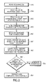
Referring to FIGS. 1 and 2, after the CPU 14 completes writing into the COP_SEND register 24, the DTL 20 takes over the management of the associated transaction 33. In operation 35A the DTL 20 reads the value in the resource ID field 24A, in operation 24B reads the value in the response count field 24B, and in operation 35C reads the value in the acknowledge count field 24C. Other fields such as a wait field and a release field may also be read. The operations performed by the DTL 20 pursuant to values in some of these other COP_SEND fields are described in more detail below.
In operation 35D, the DTL 20 formats and sends a command 30 for the descriptor 18 to the resource 36 identified in field 24A. The DTL 20 monitors any transaction response 32 received back from resource 36 in operation 35E. In operation 35F, the returned response 32 is written into the pre-allocated region in RBUF 26 until the expected response count in field 24B has expired. Response data 32 received after this point is still tracked in operation 35G, but considered resource acknowledgments and discarded.
Operation 35F compares the total amount of returned response data 32 with the acknowledgement count in field 24C. The DTL 20 generates an exception in operation 351 if the total amount of returned response data does not equal the acknowledgement count value in field 24C. Otherwise the transaction completes successfully in operation 35J.
The DTL 20 does not need to parse the data in CFIFO 22 prior to issuing the commands 30 to the resource interconnect 34 (FIG. 1). In particular, the DTL 20 does not need to be aware of the structure of the command 30, does not need to determine how many commands 30 are batched together to form a single transfer, and does not need to determine the proper amount of response data 32 to expect. This information is provided by the CPU 14 which determines and programs the expected amount of response data 32 into response count field 24B and acknowledge count field 24C of COP_SEND register 24.
For example, the descriptor 18 generated by the CPU 14 may include two instructions 19A and 19B. Possibly, only response data for the first instruction 19A may need to be stored in the RBUF 26. For instance, the first instruction 19A may be a read instruction that returns data from memory while the second instruction 19B may be a write instruction that is not expected to return data and only returns an acknowledgement.
Accordingly, the CPU 14 may write a value of 1 into the response count field 24B directing the DTL 20 to only store a first group of data in RBUF 26. The CPU 14 also writes a value of 2 into the acknowledge count field 24C of COP_SEND register 24. This notifies the DTL 20 that two sets of information should be returned from the resource 36, one set for instruction 19A, and one set for instruction 19B.
Descriptor Transfer Handles
The DTL 20 uses a scheme which allows software 15 to easily track status of transactions 33. Central to this scheme is the concept of a handle, which provides a unique identifier for every transaction 33 issued via writing to the COP_SEND register 24. FIG. 3 shows how the handle is used in the DTL 20 and FIG. 4 shows one example of a handle 40 that may be generated by control logic 50 in the DTL 20 shown in FIG. 3.
Referring both to FIGS. 3 and 4, once a complete descriptor 18 has been loaded into CFIFO 22, the CPU 14 writes to the COP_SEND register 24 to initiate a new transaction 33. In response, the logic 50 generates a handle 40 associated with that particular transaction 33. The handle 40, or some version of the handle 40, is then stored in the COP_SEND_SELECT register 54 and in RBUF 26. The handle 40 is then read back by the CPU 14 from the COP_SEND_SELECT register 54 to quickly identify the status and response information 32 for the associated transaction 33. The processor 16 (FIG. 1) reads the handle from the COP_SEND_SELECT register 54 after initiating a transaction and then stores it in memory. Some time later, the processor 16 can use the handle to identify the status and response information for the associated transaction.
A handle counter 52 increments every time the COP_SEND register 24 is written initiating a new transaction 33. The handle counter 52 is used to generate unique values for the handle within the confines of a same thread. In other words, each transaction 33 has an associated handle, and each handle contains a unique value associated with that transaction. When the CPU 14 writes to the COP_SEND register 24, the control logic 50 generates a new handle 40 and assigns that handle to the new transaction 33. As part of this process, an unused RBUF region 26A-26D is selected by the control logic 50 to receive the response data 32 for transaction 33. A corresponding pointer to the allocated RBUF region is loaded into an RBUF region ID field 42A in the handle 40 (see FIG. 4).
The control logic 50 sets a valid bit field 42C in the handle 40 indicating a valid handle. The control logic 50 may also set a wait field 42D in the handle 40 according to the setting of a corresponding wait field 24H in the COP_SEND register 24 (see FIG. 5).
A release RBUF field 42E in the handle 40 is assigned based on the value of a release resource field 24G in the COP_SEND register 24. A current value of the handle counter 52 in FIG. 2 is captured by the control logic 50 and assigned to the transaction ID field 42F in the handle 40. The counter 52 is then incremented by the control logic 50. An error field 42G may be initially set to zero. Later, if the associated transaction 33 results in an error, the control logic 50 can change the value in error field 42G.
The new handle 40 is stored in the DTL 20 and remains valid until released by the CPU 14. Once the handle 40 is generated, software 15 (FIG. 1) may retrieve the handle 40 and later use it to perform management functions associated with the associated transaction 33 or to locate the response data 32 stored in RBUF 26 for the completed transaction 33. These management functions are initiated by the CPU 14 reading or writing various DTL registers 24, and 54-60. The details of each of these registers and their associated function are described below.
The RBUF region ID field 42A of the handle 40 is typically used to select one of the four RBUF regions 26A-26D for execution of an operation. To perform a handle comparison, both the valid bit in the handle provided by the CPU 14 and the handle 40 stored with the RBUF region 26 are set, indicating validity. The count field 42F of the handle 40 is then compared to the count field of the handle 40 associated with the RBUF 26. If the count fields 42F are identical, then the handles match.
The handle comparison can be overridden and the RBUF region state accessed directly by using the skip count field 42B of the handle 40. Setting the skip count field 42B suppresses the count field comparison and valid bit checking between the handle 40 associated with RBUF 26 and the handle 40 provided by the CPU 14. Setting the skip count field 42B allows exception handlers and other entities in the DTL 20 which have no knowledge of specific descriptor handles to still access data and state information in RBUF 26.
COP_SEND
Referring to FIGS. 3 and 5, reading the COP_SEND register by the CPU 14 returns the count of data words pushed onto the CFIFO 22. Specifically, the count represents the number of data words written to CFIFO 22 since the last write of COP_SEND 24. The control logic 50 maintains this count which is incremented for every write to the CFIFO 22, decremented at every read to CFIFO 22, and is cleared when the CPU 14 writes to the COP_SEND register 24.
Writing the COP_SEND register 24 instructs the control logic 50 to begin transferring the next command 30 to the resource identified in resource ID field 24A. The data transferred in command 30 includes all of the descriptor entries written into CFIFO 22 since the last write to the COP_SEND register 24 by the CPU 14. The control logic 50 also tracks the number of data words in CFIFO 22 which is then cleared each time the CPU 14 writes to the COP_SEND register 24.
As described above, the response count field 24B is loaded by the CPU 14 to identify the amount of response data 32 the control logic 50 needs to save in the RBUF 26. As also described above, the acknowledge count field 24C is loaded by the CPU 14 to identify the amount of data expected to be returned in response 32. The acknowledge count field 24C allows the control logic 50 to determine when a particular transaction 33 has been successfully completed.
A disable exceptions field 24D causes the DTL 20 to disable some or all exception notifications. However, other error codes generated by the resources 36 may still be written into the RBUF 26. These exceptions are described in more detail below. A disable time exception field 24E disables the control logic 50 from generating an exception when a transaction 33 has not completed after some particular time period.
If a resource ID valid field 24F is set, the control logic 50 in FIG. 3 assumes that a valid encoded resource ID resides in the resource ID field 24A of the COP_SEND register 24. In this case, the value in resource ID field 24A is simply copied into the requisite channel and RBUF region. If the resource ID valid field 24F is cleared, the control logic 50 assumes that a second entry read from CFIFO 22 contains the target address of the transaction 33.
A wait (block until complete) field 24H when set by the CPU 14 causes the control logic 50 to provide a stall signal back to the CPU 14 until a particular transaction 33 has completed. The CPU 14 is automatically stalled after writing the COP_SEND register 24 with the wait field 24H set. This is similar to a stall caused by the DTL 20 when the CPU writes a handle into a COP_RBUF_WAIT register 58 described below. However, the CPU 14 is immediately stalled at the initiation of a transaction 33 when the wait field 24H is set, but the stall can be somewhat delayed by selectively writing to the COP_RBUF_WAIT register 58. Setting the wait field 24H in COP_SEND register 24 also serves to save some CPU instructions since the CPU 14 does not have to also manipulate the handle in the COP_RBUF_WAIT register 58.
A release resource field 24G notifies the control logic 50 to automatically release allocated space in the RBUF 26 for a particular transaction after that transaction is completed. When set, the release resource field 24G tells the control logic 50 to immediately release RBUF resources and the handle when the associated transaction completes. If the field is clear, resources/handle are not released until the COP_RBUF_RELEASE register 60 is accessed with the proper handle. Setting the release field 24G in COP_SEND register 24 allows the CPU 14 to essentially “fire and forget” a transaction where it does not need to keep track of any returned data or acknowledgement. The release resource field 24G may be used for example for a write transaction that does not return data back in the response 32.
In addition to these functions, the control logic 50 conducts several other operations when the CPU 14 writes to the COP_SEND register 24. First, an RBUF region 24 is selected to receive response data 32 for the transaction 33. In one embodiment, it is guaranteed that at least one unused RBUF region 24 is available. If all the RBUF regions 24A-24D are in use, the control logic 50 sends an exception to the CPU 14.
The handle state for the selected RBUF region 24 is updated with the handle 40 associated with the transaction 33. To accomplish this, the current value of the handle counter 52 is read and stored in the count field 42F of handle 40. In addition, as described above, other values are extracted from the COP_SEND register 24 and stored in the appropriate fields of handle 40. Finally, the valid bit field 42C of the handle 40 is set confirming a valid handle.
COP_SEND_SELECT
Reading a COP_SEND_SELECT register 54 by the CPU 14 returns the last handle 40 written to the register 54. Writing the COP_SEND_SELECT register 54 updates the register 54 with a new descriptor handle 40. Although the COP_SEND_SELECT register 54 can be written by the CPU 14, generally it provides the last handle generated by the control logic 50 from a write of COP_SEND register 24. The COP_SEND_SELECT register 54 is read by the CPU 14 to acquire the handle generated by the last transaction launch pursuant to a write to COP_SEND register 24.
COP_RBUF_HANDLE
Reading a COP_RBUF_HANDLE register 56 conditionally returns the handle 40 stored in one of the four RBUF regions 26. The RBUF region 26 selected is based on the RBUF region ID field 42A for the handle 40 stored in the COP_SEND_SELECT register 54. The return of valid data may be conditional, in that the handle stored in COP_SEND_SELECT register 54 may be required to match the handle stored in the indexed RBUF region 26. If the handles do not match, an error may be returned.
Writing to the COP_RBUF_HANDLE register 56 conditionally updates the handle 40 stored in an associated region of the RBUF 26. The selected RBUF region 26A-26D is based on the RBUF region ID field 42A in the handle 40. When writing the COP_RBUF_HANDLE register 56, the new handle is provided as write data from the CPU 14. The value in RBUF region ID field 42A (FIG. 4) is extracted from this write data handle. The update of the RBUF region state may be conditional in that the handle 40 provided by the CPU 14 as write data may be required to also match the handle 40 associated with the RBUF region 26.
COP_RBUF_WAIT
The CPU 14 reads the COP_RBUF_WAIT register 58 to determine whether a transaction 33 is still outstanding or has completed. The control logic 50 uses the RBUF region ID field 42A of the handle 40 stored in the COP_SEND_SELECT register 54 to select one of the RBUF regions 26A-26D, and returns completion status information 58A for the transaction 33 associated with that identified RBUF region 26. If the transaction 33 associated with the handle 40 is still outstanding, a first value 58A may be returned when reading COP_RBUF_WAIT register 58, otherwise a different value 58A is returned indicating the transaction 33 has completed.
The return of valid status information 58A from COP_RBUF_WAIT register 58 may be conditional, in that the handle 40 stored in COP_SEND_SELECT register 54 may also be required to match the handle 40 stored in the indexed RBUF region 26A-26D. If the handle 40 in COP_SEND_SELECT register 54 does not match handle associated with the indexed RBUF region 26, then reading COP_RBUF_WAIT register 58 may return a same default value 58A regardless of the completion status of the associated transaction 33.
Writing to the COP_RBUF_WAIT register 58 by the CPU 14 causes the control logic 50 to stall the CPU 14 until the transaction 33 has completed. The write data delivered to the COP_RBUF_WAIT register 58 contains the handle 40. The handle 40 is assumed to have been managed somewhere by software 15 (FIG. 1). The RBUF region ID field 42A for this handle 40 selects an RBUF region 26A-26D, and the CPU 14 is stalled based on the completion status of the transaction 33 associated with the identified RBUF region 26.
The CPU 14 will be stalled if the wait field 42D is set for the handle 40 associated with the RBUF 26 and the associated transaction 33 has not completed. Writing to the COP_RBUF_WAIT register 58 automatically sets the value in wait field 42D for the identified RBUF handle 40. The state of handle 40 associated with the RBUF region may be conditional, in that the handle written into COP_RBUF_WAIT register 58 may also be required to match the handle stored in the RBUF region 26.
The stall generated by COP_RBUF_WAIT register 58 prevents the CPU 14 from having to constantly poll the DTL 20 for transaction status. For example, the control logic 50 generates a stall signal on control line 55 to the CPU 14 while the transaction 33 is still pending. The stall signal on control line 55 is de-asserted as soon as the control logic 50 determines the transaction 33 has completed. The CPU 14 accordingly can then continue processing operations.
For example, the CPU 14 may write to the COP_RBUF_WAIT register 58 for a transaction 33 that requests a lock on a particular portion of data. The CPU 14 knows that no further operations may be performed on the requested data until the transaction 33 requesting the lock is completed. The CPU 14 is free to operate other threads and issue other transactions while the thread associated with the lock transaction 33 is stalled. As soon as the lock transaction is completed, the control logic 50 removes the stall signal from control line 55 and the thread that previously wrote to the COP_RBUF_WAIT register 58 can continue processing.
As described above, the control logic 50 tracks the acknowledge count identified in field 24C of the COP_SEND register 24. When the acknowledgement count for the transaction 33 reaches the value set in field 24C (FIG. 5) of the COP_SEND register 24, the control logic 50 removes the stall signal on control line 55 to the CPU 14. The control logic 50 performs a similar operation when the wait field 24H is set in the COP_SEND register 24.
COP_RBUF_RELEASE
When the CPU 14 reads a COP_RBUF_RELEASE register 60, the association is released between a particular handle 40 and an RBUF region 26. In effect, this operation invalidates the RBUF state of the RBUF region 26. However, data in the RBUF 26 may be unaffected. At that point, it may not be possible to perform handle-based operations on the data or on the state information in that particular RBUF region 26. The state of the RBUF region 26 may be released by clearing an associated valid bit 27.
When the CPU 14 reads COP_RBUF_RELEASE register 60, an address pointer is returned (RBUF region ID) for the data in the RBUF region 26 containing the response data 32 for the transaction 33. The return of valid data from the COP_RBUF_RELEASE register 60 and the clearing or release of the associated RBUF region 26 is conditional. For example, the handle 40 associated with the COP_SEND_SELECT register 54 may be required to match the handle 40 stored in the indexed RBUF region 26. If the two handles do not match, the read operation may return a release abort value and the state of the referenced RBUF region 26 may remain unaffected.
Writing to the COP_RBUF_RELEASE register 60 is also used for releasing the association of a handle 40 with a particular RBUF region 26, in the same manner as a read from the COP_RBUF_RELEASE register 60. However, since this operation is a write, an address pointer to the associated region in RBUF 26 is not returned.
It is worth noting that the region in RBUF 26 upon which the write operation executes may be selected not by the contents of the COP_SEND_SELECT register 54, but by the handle 40 delivered in the write operation. The RBUF ID field 42A in the handle 40 selects an RBUF region 26. As with the read of COP_RBUF_RELEASE register 60, execution of a write to the COP_RBUF_RELEASE register 60 clears a valid bit 27 in the selected RBUF region 27. The update of the RBUF region state can also be conditional, in that the handle 40 referenced in the COP_RBUF_RELEASE command may be required to match the handle 40 stored in the referenced region of RBUF 26.
Accessing COP_RBUF_RELEASE 60 ensures that RBUF resources are released, preventing future resource conflicts. Handles are also released, decreasing the burden on software for managing large numbers of handles.
FIG. 6 provides a summary of some of the handle based operations performed by the DTL 20. In operation 80, the DTL 20 detects the CPU 14 writing to the COP_SEND register. This causes the DTL 20 in operation 82 to automatically generate a handle with a unique transaction identifier. In operation 84, the DTL 20 identifies a free region in the RBUF 26 and associates the identified RBUF region with the handle. For example, the DTL 20 loads an RBUF region ID field 42A with the location of the identified RBUF region 26 and stores the unique transaction identifier into transaction ID field 42F. In operation 86, the DTL 20 stores the handle in the COP_SEND_SELECT register 54 which can then be subsequently referenced by the CPU 14.
If the CPU 14 accesses the COP_RBUF_WAIT register 58 in operation 88, and the handle associated with that register matches the handle for the associated region of RBUF 26, then the DTL 20 stalls the CPU 14 in operation 90. When the CPU 14 accesses the COP_RBUF_RELEASE register 60 in operation 92, and the handle associated with that register matches the handle in the associated RBUF region, the control logic 50 in operation 94 provides the CPU 14 with a pointer to the RBUF region that contains the response data 32 for the transaction 33. The DTL 20 then automatically releases the handle identifier and the RBUF region for use by another transaction.
Hiding Hardware Constraints
Referring to FIG. 7, the DTL 20 abstracts or, in essence, hides certain hardware constraints and states from the CPU 14. As a result, the CPU 14 does not have to use processing cycles to monitor the availability of hardware resources when initiating transactions. Alternatively, these hardware resources are monitored by the DTL 20 and whenever an actual constraint is detected, a notification is sent from the DTL 20 to the CPU 14 possibly causing the CPU 14 to stall or alter processing operations. This relieves the CPU 14 from having to determine which entries 23 in the CFIFO 22 currently contain descriptor data 18, which descriptor entries 23 have been sent to resources, and which entries 23 are available in CFIFO 22 for loading more descriptor data 18.
In a first CFIFO interlock operation, the DTL control logic 50 tracks the number of available entries 23 by reading a depth value 116 from CFIFO 22. If all of the entries in CFIFO 22 are filled with descriptor data and the CPU 14 tries another write 112 to the CFIFO 22, the control logic 50 generates a CFIFO stall signal 106 that stops the CPU 14 from loading more data into CFIFO 22. When CFIFO entries 23 become free, the control logic 50 removes the CFIFO stall signal 106 and the CPU 14 continues loading descriptor data into CFIFO 22.
In a second DTL interlock operation, the DTL control logic 50 monitors the busy status 118 of two CFIFO channels 100 and 102 that can simultaneously send commands 30 from CFIFO 22 over the interconnect 34. Both CFIFO channels 100 and 102 may currently be busy as indicated by channel busy signal 118. If the CPU 14 tries to initiate another transaction by writing to the COP_SEND register 24 via write signal 114 during the asserted channel busy signal 118, the control logic 50 generates a channel stall signal 108 that causes the CPU 14 to stall the write 114 to the COP_SEND register 24.
When either of the channels 100 or 102 are no longer busy, the control logic 50 removes the channel stall signal 108 and the CPU 14 can then initiate the transaction by writing to COP_SEND register 24. This eliminates the CPU 14 from having to keep track of the number and status of the CFIFO channels. When only the channel stall signal 108 is generated and the CFIFO stall signal 106 is not currently asserted, the CPU 14 may continue to load descriptor data 18 into CFIFO 22 as long as there are available entries 23. The CPU 14 is also able to perform other operations that do not initiate transactions.
A third RBUF interlock operation manages the RBUF regions 26A-26D. As described above, the CPU 14 may send a write command 114 to the COP_SEND register 24 to initiate a new transaction previously queued in the CFIFO 22. In response to the COP_SEND register write 114, the control logic 50 tries to allocate a free region in RBUF 26. If all of the regions 26A-26D in RBUF 26 are currently allocated, the control logic 50 sends an error signal which causes an exception in the CPU 14. Valid bits 104A-104D in the RBUF regions 26A-26D, respectively, or some indicator, may be used to indicate the current allocation status.
The RBUF error signal 110 causes the CPU 14 to cancel the write 114 to COP_SEND register 24. The exception taken by the CPU 14 may invoke an exception handler routine that causes the CPU 14 to possibly scan through the regions in RBUF 26 that may be associated with completed transactions. The CPU 14 can then store the data from RBUF regions with completed transactions in other memory and release the handle and associated RBUF region. Software 15 may then return from the exception in a manner which allows the original write 114 to the COP_SEND register 24 to be reissued.
A COP_SEND_COUNT register 52 was briefly described above in FIG. 3 and is used to store the current unique handle value for a transaction. The handle value in counter 122 is incremented by the control logic 50 each time the CPU 14 successfully writes to the COP_SEND register 24 and initiates a new transaction. Any time the counter 122 reaches a highest value, a rollover exception is generated on the next write to COP_SEND register 24. The value in COP_SEND_COUNT register 52 can be written by the CPU 14, and the write data is then written to the counter 122. This allows the CPU 14 to control the count value, and, indirectly, can effect when a count limit is reached. When the count limit is reached, the control logic 50 generates an out of handle exception 111. The out of handle exception 111 then causes the CPU 14 to cancel the write 114 to the COP_SEND register 24.
The out of handle exception 111 can be used by the CPU 14 for debugging or to let the CPU 14 know when the DTL 20 is running out of unique transaction identifiers. For example, the count value can be set so that the highest count value is reached before an actual count overflow. The CPU 14 can then reset the counter 122 when all outstanding transactions have completed. This ensures unique handle values are used for all subsequent transactions.
The count value can also be used to set to some value that is associated with a processing error. For example, any group of transactions that cause the value in register 52 to reach some predetermined value may correspond to a processing error. The count value can be selected to notify the CPU 14 of these particular types of processing errors.
Transaction Errors
Referring to FIG. 8, the DTL 20 may also generate other types of exception signals that are not associated with hiding hardware constraints. In some cases the control logic 50 will also save an error code which describes the class of error detected. A CFIFO overflow error signal 130 is generated by the control logic 50 when the CPU 14 writes too much data into the CFIFO 22 at one time without writing to COP_SEND register 24. The control logic 50 keeps track of the writes 112 to the CFIFO 22 and the writes 114 to the COP_SEND register 24. When the number of CFIFO writes 112 reaches some limit without the issuance of a COP_SEND write 114, the control logic 50 generates the CFIFO signal 130 indicating a programming error.
The DTL control logic 50 may also generate a zero acknowledge exception 132 when the CPU 14 loads a zero value into the acknowledge count field 24C of the COP_SEND register 24. Other exceptions can also be generated by the control logic 50 when the CPU 14 loads illegal values into any fields in any DTL registers that have been described above. The control logic 50 can also generate exception signals for parity errors for data in the RBUF 26 and can generate timeout errors when a particular transaction takes too much time to provide a response 32 (FIG. 1). These timeout values can be set in a DTL register by the CPU 14.
A transfer response error signal 134 is generated by the control logic 50 to notify the CPU 214 of a mismatch between the actual amount of response data 144 received by the control logic 50 and the amount of expected response data as specified by the value in acknowledge count field 24C. The control logic 50 may detect the mismatch when the response data 134 contains an end bit before the acknowledge count value have been reached or when the received response data reaches the acknowledge count before the end bit is received.
Resource Errors
A resource error is signaled when the error code returned from a resource is non-zero. Upon this detection, the DTL control logic 50 signals a resource error 136 to the CPU 14 and stores the error code at the end of the RBUF region 26 associated with the transaction. This immediately causes the CPU 14 to jump to an error handler routine where the error code 146 is read from the RBUF 26. Storing error codes 146 in the RBUF 26 eliminates having to provide special error registers.
Disabling Exceptions
As previously described above in FIG. 5, the CPU 14 can also write a value into the disable exception field 24D of the COP_SEND register 24 to prevent the control logic 50 from generating all or most types of the exception signals described above. A disable time field 24E of the COP_SEND register 24 is set by the CPU 14 to disable the control logic 50 from generating the timeout error signal described above. For example, certain packet processing transactions may never complete until a packet is received by a router or switch using the PPE 12 in FIG. 1. Accordingly, the CPU 14 can set field 24E for any transactions that may take an indeterminate amount of time to complete.
Memory Operations
FIG. 9 shows how the DTL 20 can also be used for memory operations. A memory system 160 may also be used as part of the PPE 12. The memory system 160 may include a data cache 162 and associated tags 161. The memory system 160 may also include a read buffer 164, a pre-fetch buffer 166, and a write buffer 168. The DTL 20 creates descriptors and manages associated transactions when the memory system 160 needs to access other memory resources.
With respect to the descriptors 18 generated by the CPU 14, the DTL 20 operates in the same manner as described above. The descriptor 18 is loaded into the CFIFO 22 and then output through one of the two CFIFO channels 100 or 102 as DTL commands 30. The DTL responses 32 are then stored in the appropriate region of RBUF 26. The CPU 14 then uses the RBUF pointer in handle 40 to read the response data 32 from RBUF 26.
If the CPU 14 conducts a read operation with an address 170 that misses with tags 161, the load miss is converted by logic 185 into a read descriptor. The read descriptor is loaded into a read buffer channel 186 and then output as a read command 187. The associated read response 194 returned back from the memory resource is loaded by the DTL 20 into the read buffer 164 and then the addressed data loaded into the cache 162.
The CPU 14 may generate a pre-fetch read request 178 that includes a pre-fetch address. The DTL 20 includes logic 190 that converts the pre-fetch read request into a descriptor. The logic 190 loads a command into a pre-fetch buffer channel 191 that then sends a pre-fetch read command 196 to the targeted memory resource. A pre-fetch response 195 is received back by the DTL 20 and forwarded to the pre-fetch buffer 166. If a subsequent read misses in cache 162, the pre-fetch buffer 166 can be interrogated. If the pre-fetch buffer 166 contains data for the requested address, the contents in pre-fetch buffer 166 are loaded into cache 162.
The CPU 14 may try to store data in cache 162. If the address 170 misses with the tags 161, the data is written into the write buffer 168. The logic 192 then converts the data in write buffer 168 into a descriptor. The logic 192 then loads a write command into write buffer channel 193 that then sends the write data out to the memory resource as a write command 197. The resource may respond back with an acknowledge response 198.
Multi-Threaded CPU
Referring to FIG. 10, the CPU 14 may operate multiple different software thread states 16A-16D. Separate DTLs 20A-20D are each associated with the different thread states 16A-16D in CPU 14, respectively. The DTLs 20A-20D each include the same registers and operate similarly to the DTL 20 described above. Each thread 16A-16D also has individual CFIFO channels, write buffer channels, read buffer channels and pre-fetch channels as also described above in FIG. 9.
The multithreaded CPU 14 can use software processing cycles previously used for managing a transaction 33 to now execute operations in the same or other threads. For example, a first thread 16A in the CPU 14 may send a descriptor to the associated DTL 20A. The thread 16A in the CPU 14 can then conduct other operations while the DTL 20A is managing the previously initiated transaction. Even if the thread 16A can not perform other tasks until a response to the descriptor is received back from a resource, the CPU 14 can still use the processing cycles previously spent managing that transaction to perform tasks in other threads 16B-16D.
Network Processor
FIG. 11 is a block diagram of a multi-threaded network processor 200. The packet processor 200 is described in co-pending patent application Ser. No. 11/054,076, filed Feb. 8, 2005, entitled: MULTI-THREADED PACKET PROCESSING ARCHITECTURE, which is herein incorporated by reference.
Packets 201 are received by the packet processor 200 and typically stored in a Global Packet Memory (GPM) 204 via a multiplexer 202. After a packet is received, the GPM 204 builds an associated packet handle data structure and then enqueues the packet on a flow lock queue operated by a lock manager and resequencer 220. After receiving a reply back from the lock manager 220, the GPM 204 directs a distributor 206 to allocate the packet 201 to Packet Processing Elements (PPEs) 12 similar to those described above in FIGS. 1-10.
The PPEs 12 process the packets in the GPM 204 through a resource interconnect 208. The PPEs 210 may also use a Level-2 (L2) cache 212, Dynamic Random Access Memory (DRAM) controls 214, and lookup control 216 to access external memory 215. An external Ternary Content Addressable Memory (TCAM) 219 is also accessible by the PPEs 12 through the resource interconnect 208 and a TCAM controller 218. In one embodiment as described in FIG. 10, the PPEs 12 are multi-threaded. However, any generic processing unit with or without multi-threaded capability can be used.
The PPEs 12 inform the lock manager 220 when they have completed processing a packet. The PPEs 12 are then free to start processing other packets. After being processed by the PPEs 12, the packets continue to reside in the GPM 204 and may be stored in GPM 204 in a scattered non-contiguous fashion. A gather mechanism 222 is responsible for gathering and assembling the scattered portions of the packet back together. The lock manager 220 works with the gather mechanism 222 to determine the final order that the assembled packets 223 are sent from the GPM 204 to a Buffer, Queue, Scheduler (BQS) memory controller 224. The BQS 224 queues, schedules, and de-queues packets, offloading this time-consuming task from the PPEs 12. An external memory 225 is used by the BQS 224 as a packet buffer for, among other things, storing packets between different arrival and main processing operations. A recirculation path 232 is used by the BQS 224 to recirculate packets back to the GPM 204 for further processing by the PPEs 12.
Various specialized packet processing assists, such as a Forwarding Information dataBase (FIB) look-up, the TCAM access controller 218, atomic operations to memory, policers, Weighted Random Early Detection (WRED), hashing and modulus, and any other resource can also be used in the packet processor 200 to provide increased performance levels. Packet processing assists can also provide hardware atomic updates of known data structures in order to allow high performance updates to structures that represent large bandwidth flow through the network processor.
Resources in the packet processor 200 refer to any of these different functional elements that can be accessed by the PPEs 12. For example, the L-2 cache 212, external memory 215, external TCAM 219, GPM 204, and other co-processors are all considered resources.
The system described above can use dedicated processor systems, micro controllers, programmable logic devices, or microprocessors that perform some or all of the operations. Some of the operations described above may be implemented in software and other operations may be implemented in hardware.
For the sake of convenience, the operations are described as various interconnected functional blocks or distinct software modules. This is not necessary, however, and there may be cases where these functional blocks or modules are equivalently aggregated into a single logic device, program or operation with unclear boundaries. In any event, the functional blocks and software modules or features of the flexible interface can be implemented by themselves, or in combination with other operations in either hardware or software.
Having described and illustrated the principles of the invention in a preferred embodiment thereof, it should be apparent that the invention may be modified in arrangement and detail without departing from such principles. I claim all modifications and variation coming within the spirit and scope of the following claims.

Claims (20)

1. An apparatus, comprising:
descriptor transfer logic coupled between a programmable general purpose processing element and resources and configured to receive descriptors generated by the processing element and manage transactions that sends the descriptors to the resources for execution and receives responses back from the resources in response to the sent descriptors,
the descriptor transfer logic further configured to manage the allocation and operation of buffers and registers that initiate the transaction, track the status of the transaction, and receive the responses back from the resources independently from the processing element, the descriptor transfer logic including a Command First-In First-Out buffer (CFIFO) configured to buffer multiple different batched resource instructions contained in the same or multiple different descriptors received from the processing element, and the descriptor transfer logic further configured to manage the transfer of the resource instructions from the CFIFO to the resources.
2. The apparatus according to claim 1 wherein:
the processing element comprises a Central Processing Unit (CPU) configured to generate the descriptors independently of the descriptor transfer logic;
the resources comprise multiple different computer or co-processing elements that process the resource instructions in the descriptors independently of the CPU;
the descriptor transfer logic is coupled between the CPU and through an interconnect to the multiple different computer or co-processing elements;
the CFIFO includes an input coupled to the CPU and an output coupled through the interconnect to the multiple different computer or co-processing elements; and
the descriptor transfer logic manages for the CPU monitoring the status of the resource instructions sent from the CFIFO to the resources.
3. The apparatus according to claim 2 wherein the descriptor transfer logic includes a send register that when written to by the CPU indicates to the descriptor transfer logic that a complete descriptor has been loaded into the CFIFO by the CPU and causes the descriptor transfer logic to take over management of the descriptor from the CPU and initiate the transaction for the descriptor currently in the CFIFO and associate subsequently loaded data in the CFIFO with a new descriptor.
4. The apparatus according to claim 3 wherein the descriptor transfer logic includes multiple channel buffers coupled between the CFIFO and the interconnect, wherein the channel buffers are configured to send out commands from the CFIFO, and the descriptor transfer logic is configured to generate a stall signal to the CPU preventing the CPU from writing to the send register when all of the channel buffers are busy.
5. The apparatus according to claim 3 wherein the send register includes a resource Id field identifying the resources targeted for the transaction associated with the descriptor in the CFIFO, a count field identifying an amount of buffer space the descriptor transfer logic should allocate to the transaction associated with the descriptor loaded in the CFIFO, and an acknowledge field indicating an amount of data the descriptor transfer logic should monitor for the transaction associated with the descriptor loaded in the CFIFO.
6. The apparatus according to claim 2 including a response buffer coupled between the CPU and the interconnect and having multiple regions each allocated to different transactions by the descriptor transfer logic independently of the CPU.
7. The apparatus according to claim 6 wherein the descriptor transfer logic generates a stall signal preventing the CPU from writing to the send register when the CPU tries to initiate a new transaction while all of the regions in the response buffer are already allocated.
8. A method comprising:
receiving descriptors with descriptor transfer logic, wherein the descriptors are generated by a programmable Central Processing Unit (CPU) and the descriptor transfer logic is located between the CPU and resources and the resources are other processors or memory used by the CPU for processing data;
managing a transaction for the CPU with the descriptor transfer logic, wherein the transaction includes the descriptor transfer logic sending the descriptors to the resources for execution;
receiving with the descriptor transfer logic responses back from the resources in response to the sent descriptors;
managing allocation and operation of buffers and registers that initiate the transaction, track the status of the transaction, and receive the responses back from the resources with the descriptor transfer logic independently of the CPU; and
providing the responses to the CPU for further processing.
9. The method according to claim 8 further comprising:
buffering multiple different batched resource instructions contained in the same or multiple different descriptors received from the CPU in a First In-First Out Buffer (FIFO) within the descriptor transfer logic, wherein the FIFO has an input coupled to the CPU and an output coupled through an interconnect to the resources;
monitoring for write operations from the CPU to a send register in the descriptor transfer logic;
initiating transfer of the batched resource instructions with the descriptor transfer logic responsive to the CPU writing to the send register; and
managing the transfer of the batched resource instructions from the FIFO to the resources with the descriptor transfer logic.
10. The method according to claim 8 further comprising:
receiving multiple different threads each independently operating different descriptor transfer logic, the different descriptor transfer logic each coupled between the CPU and the resources and each comprising separate command buffers, send registers, response buffers, and control logic configured to separately manage the transfer of commands to the resources and manage the receiving of associated responses data back from the resources.
11. The apparatus according to claim 2 wherein the description transfer logic includes control logic configured to generate handles associated with the descriptors in the CFIFO.
12. The apparatus according to claim 11 wherein the control logic is configured to assign a unique transaction identifier for each handle, allocate a region of a response buffer located in the descriptor transfer logic to the transaction, and identify the allocated region in the handle.
13. The apparatus according to claim 12 wherein the control logic is configured to compare a first handle currently being referenced by the CPU with a second handle currently associated with a region in the response buffer referenced by the first handle, and conditionally execute operations according to the comparison between the first and second handle.
14. The apparatus according to claim 11 wherein the descriptor transfer logic includes a wait register that when written to by the CPU causes the control logic to stall the CPU.
15. The apparatus according to claim 14 wherein the descriptor transfer logic includes a release register configured to reserve a region in the response buffer and further configured to release that region in the response buffer.
16. The apparatus according to claim 1 including multiple different independently operating descriptor transfer logic each configured to independently manage transactions for different threads operated by the processing element.
17. An apparatus, comprising:
a general purpose programmable processor core;
resources comprising multiple different computer or co-processing elements configured to perform operations responsive to commands contained in descriptors generated by the processor core;
descriptor transfer logic coupled between the processor core and through an interconnect to the resources, wherein the descriptor transfer logic includes:
a command buffer configured to buffer the descriptors generated by the processor core;
a send register configured to control management of the descriptors in the send register, initiation of associated transactions, and management of buffer transaction parameters associated with the descriptors;
a response buffer configured to storage response data associated with the transactions; and
control logic configured to manage handles for each of the transactions that include different fields that each contain different status information for the transactions, wherein the handles are stored in handle registers and read by the processor core to determine the status information for the transactions.
18. The apparatus according to claim 17 wherein each of the handles includes:
an identifier field containing a value uniquely identifying an associated transaction;
a pointer field containing a pointer value to a region in the response buffer where data from the associated transaction is stored; and
a wait field containing a value for stalling the processor core.
19. The apparatus according to claim 17 wherein the send register includes:
a resource Id field identifying the resources;
a response count field configured to manage an amount of total response data associated with the transactions, and
an acknowledge count field configured to manage an amount data associated with the transactions.
20. The method according to claim 8 further comprising:
writing data into a send register;
generating a unique handle identifier for the transaction according to data in the send register;
identifying and allocating a region of a response buffer to the transaction;
storing a pointer in the handle pointing to the region of the response buffer allocated to the transaction;
storing the handle in a select register for subsequent referencing by the CPU;
monitoring the CPU for access to the region of the response buffer; and
releasing the handle and the region of the response buffer after being accessed by the CPU.
US11/555,066 2005-10-31 2006-10-31 Descriptor transfer logic Active 2027-12-25 US7739426B1 (en)

Priority Applications (1)

Application Number Priority Date Filing Date Title
US11/555,066 US7739426B1 (en) 2005-10-31 2006-10-31 Descriptor transfer logic

Applications Claiming Priority (2)

Application Number Priority Date Filing Date Title
US73207905P 2005-10-31 2005-10-31
US11/555,066 US7739426B1 (en) 2005-10-31 2006-10-31 Descriptor transfer logic

Publications (1)

Publication Number Publication Date
US7739426B1 true US7739426B1 (en) 2010-06-15

Family

ID=42244464

Family Applications (1)

Application Number Title Priority Date Filing Date
US11/555,066 Active 2027-12-25 US7739426B1 (en) 2005-10-31 2006-10-31 Descriptor transfer logic

Country Status (1)

Country Link
US (1) US7739426B1 (en)

Cited By (5)

* Cited by examiner, † Cited by third party
Publication number Priority date Publication date Assignee Title
US20100332698A1 (en) * 2009-06-29 2010-12-30 Sun Microsystems, Inc. Efficient buffer management in a multi-threaded network interface
US8850137B2 (en) 2010-10-11 2014-09-30 Cisco Technology, Inc. Memory subsystem for counter-based and other applications
US8943205B2 (en) 2012-04-25 2015-01-27 Cisco Technology, Inc. Generalized coordinate system and metric-based resource selection framework
US9256548B2 (en) 2012-11-29 2016-02-09 Cisco Technology, Inc. Rule-based virtual address translation for accessing data
US10114638B2 (en) 2014-12-15 2018-10-30 Cisco Technology, Inc. Command message generation and execution using a machine code-instruction

Citations (75)

* Cited by examiner, † Cited by third party
Publication number Priority date Publication date Assignee Title
US4442484A (en) 1980-10-14 1984-04-10 Intel Corporation Microprocessor memory management and protection mechanism
US4491945A (en) 1982-06-25 1985-01-01 At&T Bell Laboratories Fast packet switch
US4494230A (en) 1982-06-25 1985-01-15 At&T Bell Laboratories Fast packet switching system
US4630260A (en) 1985-06-27 1986-12-16 At&T Bell Laboratories Self-routing multipath packet switching network with sequential delivery of packets
US4734907A (en) 1985-09-06 1988-03-29 Washington University Broadcast packet switching network
US4755986A (en) 1985-09-13 1988-07-05 Nec Corporation Packet switching system
US4866701A (en) 1988-09-02 1989-09-12 Bell Communications Research, Inc. Packet switch with dynamic allocation of inputs
US4893304A (en) 1988-09-02 1990-01-09 Bell Communications Research, Inc. Broadband packet switch with combined queuing
US5127000A (en) 1989-08-09 1992-06-30 Alcatel N.V. Resequencing system for a switching node
US5151988A (en) 1987-02-18 1992-09-29 Hitachi, Ltd. Intersystem data base sharing journal merge method
US5173897A (en) 1989-12-23 1992-12-22 Alcatel N.V. Method of restoring the correct cell sequence, particularly in an atm exchange, and output unit therefor
US5179551A (en) 1991-04-08 1993-01-12 Washington University Non-blocking multi-cast switching system
US5179556A (en) 1991-08-02 1993-01-12 Washington University Bandwidth management and congestion control scheme for multicast ATM networks
US5229991A (en) 1991-01-30 1993-07-20 Washington University Packet switch with broadcasting capability for atm networks
US5247629A (en) 1989-03-15 1993-09-21 Bull Hn Information Systems Italia S.P.A. Multiprocessor system with global data replication and two levels of address translation units
US5253251A (en) 1991-01-08 1993-10-12 Nec Corporation Switching system with time-stamped packet distribution input stage and packet sequencing output stage
US5260935A (en) 1991-03-01 1993-11-09 Washington University Data packet resequencer for a high speed data switch
US5327556A (en) 1991-02-15 1994-07-05 International Business Machines Corporation Fast intersystem page transfer in a data sharing environment with record locking
US5402415A (en) 1993-04-22 1995-03-28 Washington University Multicast virtual circuit switch using cell recycling
US5430850A (en) 1991-07-22 1995-07-04 Massachusetts Institute Of Technology Data processing system with synchronization coprocessor for multiple threads
US5450411A (en) 1994-09-02 1995-09-12 At&T Global Information Solutions Company Network interface for multiplexing and demultiplexing isochronous and bursty data streams in ATM networks
US5551046A (en) 1991-06-14 1996-08-27 International Business Machines Corporation Method for non-hierarchical lock management in a multi-system shared data environment
US5682537A (en) 1995-08-31 1997-10-28 Unisys Corporation Object lock management system with improved local lock management and global deadlock detection in a parallel data processing system
US5699500A (en) 1995-06-01 1997-12-16 Ncr Corporation Reliable datagram service provider for fast messaging in a clustered environment
US5842040A (en) 1996-06-18 1998-11-24 Storage Technology Corporation Policy caching method and apparatus for use in a communication device based on contents of one data unit in a subset of related data units
US5845129A (en) 1996-03-22 1998-12-01 Philips Electronics North America Corporation Protection domains in a single address space
US5845147A (en) 1996-03-19 1998-12-01 Emc Corporation Single lock command for an I/O storage system that performs both locking and I/O data operation
US5896501A (en) 1992-12-18 1999-04-20 Fujitsu Limited Multiprocessor system and parallel processing method for processing data transferred between processors
US5905725A (en) 1996-12-16 1999-05-18 Juniper Networks High speed switching device
US5949780A (en) 1997-07-11 1999-09-07 Network Machines, Inc. Integration of intelligence with communications in a switching node
US5987506A (en) 1996-11-22 1999-11-16 Mangosoft Corporation Remote access and geographically distributed computers in a globally addressable storage environment
US6032190A (en) 1997-10-03 2000-02-29 Ascend Communications, Inc. System and method for processing data packets
US6128666A (en) 1997-06-30 2000-10-03 Sun Microsystems, Inc. Distributed VLAN mechanism for packet field replacement in a multi-layered switched network element using a control field/signal for indicating modification of a packet with a database search engine
US6161144A (en) 1998-01-23 2000-12-12 Alcatel Internetworking (Pe), Inc. Network switching device with concurrent key lookups
US6163856A (en) 1998-05-29 2000-12-19 Sun Microsystems, Inc. Method and apparatus for file system disaster recovery
US6170025B1 (en) 1997-08-29 2001-01-02 Intel Corporation Distributed computer system supporting remote interrupts and lock mechanism
EP1085723A2 (en) 1999-09-20 2001-03-21 Kabushiki Kaisha Toshiba Fast and adaptive packet processing device and method using digest information of input packet
US6253273B1 (en) 1998-02-06 2001-06-26 Emc Corporation Lock mechanism
US20010049744A1 (en) 2000-03-03 2001-12-06 Terrence Hussey High-speed data processing using internal processor memory space
WO2002009307A1 (en) 2000-07-26 2002-01-31 Pluris, Inc. Method and apparatus for load apportionment among physical interfaces in data routers
WO2002039667A2 (en) 2000-11-07 2002-05-16 Fast-Chip, Inc. Switch-based network processor
US6405274B1 (en) 1998-12-30 2002-06-11 Oracle Corporation Anticipatory lock mode conversions in a lock management system
US6411983B1 (en) 1997-11-27 2002-06-25 International Business Machines Corporation Mechanism for managing the locking and unlocking of objects in Java
US6473849B1 (en) 1999-09-17 2002-10-29 Advanced Micro Devices, Inc. Implementing locks in a distributed processing system
US20020184216A1 (en) 2001-05-31 2002-12-05 Sashikanth Chandrasekaran Method and apparatus for reducing latency and message traffic during data and lock transfer in a multi-node system
US6529983B1 (en) 1999-11-03 2003-03-04 Cisco Technology, Inc. Group and virtual locking mechanism for inter processor synchronization
US6553464B1 (en) 2001-03-04 2003-04-22 Emc Corporation Obtaining data from a remote storage device
US6563790B1 (en) 1999-05-21 2003-05-13 Advanced Micro Devices, Inc. Apparatus and method for modifying a limit of a retry counter in a network switch port in response to exerting backpressure
US6601138B2 (en) 1998-06-05 2003-07-29 International Business Machines Corporation Apparatus system and method for N-way RAID controller having improved performance and fault tolerance
US20040039787A1 (en) 2002-08-24 2004-02-26 Rami Zemach Methods and apparatus for processing packets including accessing one or more resources shared among processing engines
US20040039815A1 (en) 2002-08-20 2004-02-26 Compaq Information Technologies Group, L.P. Dynamic provisioning system for a network of computers
US20040037322A1 (en) 2002-08-24 2004-02-26 Vitaly Sukonik Methods and apparatus for processing packets including distributing packets across multiple packet processing engines and gathering the processed packets from the processing engines
WO2004019571A2 (en) 2002-08-24 2004-03-04 Cisco Technology, Inc. Packet processing engine
US20040117790A1 (en) 2002-12-13 2004-06-17 Rhine Scott Alan Systems and methods for facilitating fair and efficient scheduling of processes among multiple resources in a computer system
US20040143712A1 (en) 2003-01-16 2004-07-22 International Business Machines Corporation Task synchronization mechanism and method
US20050015686A1 (en) 2003-07-16 2005-01-20 International Business Machines Corporation Buckets of commands in a multiprocessor-based verification environment
US20050100017A1 (en) 2003-11-12 2005-05-12 Cisco Technology, Inc., A California Corporation Using ordered locking mechanisms to maintain sequences of items such as packets
US6920447B2 (en) 2001-02-15 2005-07-19 Microsoft Corporation Concurrent data recall in a hierarchical storage environment using plural queues
US20050163143A1 (en) 2004-01-27 2005-07-28 International Business Machines Corporation Method, system and product for identifying, reserving, and logically provisioning resources in provisioning data processing systems
US6947425B1 (en) 1999-12-29 2005-09-20 Intel Corporation Multi-threaded sequenced transmit software for packet forwarding device
US20050216461A1 (en) 2004-03-27 2005-09-29 Cisco Technology, Inc., A California Corporation Bypassing native storage operations by communicating protected data within locking messages using a lock manager independent of the storage mechanism
US20050220112A1 (en) 2003-11-12 2005-10-06 Cisco Technology, Inc. Distributed packet processing with ordered locks to maintain requisite packet orderings
US20060179156A1 (en) 2005-02-08 2006-08-10 Cisco Technology, Inc. Multi-threaded packeting processing architecture
US7093027B1 (en) 2002-07-23 2006-08-15 Atrica Israel Ltd. Fast connection protection in a virtual local area network based stack environment
US7100020B1 (en) 1998-05-08 2006-08-29 Freescale Semiconductor, Inc. Digital communications processor
US20060221823A1 (en) 2005-04-05 2006-10-05 Cisco Technology, Inc., A California Corporation Assigning resources to items such as processing contexts for processing packets
US7120631B1 (en) 2001-12-21 2006-10-10 Emc Corporation File server system providing direct data sharing between clients with a server acting as an arbiter and coordinator
US20070008989A1 (en) 2005-06-30 2007-01-11 Intel Corporation Packet processing
US20070014240A1 (en) 2005-07-12 2007-01-18 Alok Kumar Using locks to coordinate processing of packets in a flow
US20070022084A1 (en) 2005-07-25 2007-01-25 Cohen Earl T Hashing assist for network processors
US20070022429A1 (en) 2005-07-25 2007-01-25 Mark Rosenbluth Lock sequencing
US20070050671A1 (en) 2005-08-30 2007-03-01 Markevitch James A Selective error recovery of processing complex using privilege-level error discrimination
US7210022B2 (en) 2001-05-15 2007-04-24 Cloudshield Technologies, Inc. Apparatus and method for interconnecting a processor to co-processors using a shared memory as the communication interface
US20070198792A1 (en) 2006-02-22 2007-08-23 David Dice Methods and apparatus to implement parallel transactions
US7313557B1 (en) 2002-03-15 2007-12-25 Network Appliance, Inc. Multi-protocol lock manager

Patent Citations (85)

* Cited by examiner, † Cited by third party
Publication number Priority date Publication date Assignee Title
US4442484A (en) 1980-10-14 1984-04-10 Intel Corporation Microprocessor memory management and protection mechanism
US4491945A (en) 1982-06-25 1985-01-01 At&T Bell Laboratories Fast packet switch
US4494230A (en) 1982-06-25 1985-01-15 At&T Bell Laboratories Fast packet switching system
US4630260A (en) 1985-06-27 1986-12-16 At&T Bell Laboratories Self-routing multipath packet switching network with sequential delivery of packets
US4901309A (en) 1985-09-06 1990-02-13 Washington University Cross-connect for switch modules
US4829227A (en) 1985-09-06 1989-05-09 Washington University High speed data link
US4849968A (en) 1985-09-06 1989-07-18 Washington University Buffer management system
US4734907A (en) 1985-09-06 1988-03-29 Washington University Broadcast packet switching network
US4755986A (en) 1985-09-13 1988-07-05 Nec Corporation Packet switching system
US5151988A (en) 1987-02-18 1992-09-29 Hitachi, Ltd. Intersystem data base sharing journal merge method
US4866701A (en) 1988-09-02 1989-09-12 Bell Communications Research, Inc. Packet switch with dynamic allocation of inputs
US4893304A (en) 1988-09-02 1990-01-09 Bell Communications Research, Inc. Broadband packet switch with combined queuing
US5247629A (en) 1989-03-15 1993-09-21 Bull Hn Information Systems Italia S.P.A. Multiprocessor system with global data replication and two levels of address translation units
US5127000A (en) 1989-08-09 1992-06-30 Alcatel N.V. Resequencing system for a switching node
US5173897A (en) 1989-12-23 1992-12-22 Alcatel N.V. Method of restoring the correct cell sequence, particularly in an atm exchange, and output unit therefor
US5253251A (en) 1991-01-08 1993-10-12 Nec Corporation Switching system with time-stamped packet distribution input stage and packet sequencing output stage
US5229991A (en) 1991-01-30 1993-07-20 Washington University Packet switch with broadcasting capability for atm networks
US5327556A (en) 1991-02-15 1994-07-05 International Business Machines Corporation Fast intersystem page transfer in a data sharing environment with record locking
US5260935A (en) 1991-03-01 1993-11-09 Washington University Data packet resequencer for a high speed data switch
US5339311A (en) 1991-03-01 1994-08-16 Washington University Data packet resequencer for a high speed data switch
US5179551A (en) 1991-04-08 1993-01-12 Washington University Non-blocking multi-cast switching system
US5551046A (en) 1991-06-14 1996-08-27 International Business Machines Corporation Method for non-hierarchical lock management in a multi-system shared data environment
US5430850A (en) 1991-07-22 1995-07-04 Massachusetts Institute Of Technology Data processing system with synchronization coprocessor for multiple threads
US5179556A (en) 1991-08-02 1993-01-12 Washington University Bandwidth management and congestion control scheme for multicast ATM networks
US5896501A (en) 1992-12-18 1999-04-20 Fujitsu Limited Multiprocessor system and parallel processing method for processing data transferred between processors
US5402415A (en) 1993-04-22 1995-03-28 Washington University Multicast virtual circuit switch using cell recycling
US5450411A (en) 1994-09-02 1995-09-12 At&T Global Information Solutions Company Network interface for multiplexing and demultiplexing isochronous and bursty data streams in ATM networks
US5699500A (en) 1995-06-01 1997-12-16 Ncr Corporation Reliable datagram service provider for fast messaging in a clustered environment
US5682537A (en) 1995-08-31 1997-10-28 Unisys Corporation Object lock management system with improved local lock management and global deadlock detection in a parallel data processing system
US5845147A (en) 1996-03-19 1998-12-01 Emc Corporation Single lock command for an I/O storage system that performs both locking and I/O data operation
US5845129A (en) 1996-03-22 1998-12-01 Philips Electronics North America Corporation Protection domains in a single address space
US5842040A (en) 1996-06-18 1998-11-24 Storage Technology Corporation Policy caching method and apparatus for use in a communication device based on contents of one data unit in a subset of related data units
US5987506A (en) 1996-11-22 1999-11-16 Mangosoft Corporation Remote access and geographically distributed computers in a globally addressable storage environment
US5905725A (en) 1996-12-16 1999-05-18 Juniper Networks High speed switching device
US6128666A (en) 1997-06-30 2000-10-03 Sun Microsystems, Inc. Distributed VLAN mechanism for packet field replacement in a multi-layered switched network element using a control field/signal for indicating modification of a packet with a database search engine
US5949780A (en) 1997-07-11 1999-09-07 Network Machines, Inc. Integration of intelligence with communications in a switching node
US6170025B1 (en) 1997-08-29 2001-01-02 Intel Corporation Distributed computer system supporting remote interrupts and lock mechanism
US6032190A (en) 1997-10-03 2000-02-29 Ascend Communications, Inc. System and method for processing data packets
US6411983B1 (en) 1997-11-27 2002-06-25 International Business Machines Corporation Mechanism for managing the locking and unlocking of objects in Java
US6161144A (en) 1998-01-23 2000-12-12 Alcatel Internetworking (Pe), Inc. Network switching device with concurrent key lookups
US6253273B1 (en) 1998-02-06 2001-06-26 Emc Corporation Lock mechanism
US7100020B1 (en) 1998-05-08 2006-08-29 Freescale Semiconductor, Inc. Digital communications processor
US6163856A (en) 1998-05-29 2000-12-19 Sun Microsystems, Inc. Method and apparatus for file system disaster recovery
US6601138B2 (en) 1998-06-05 2003-07-29 International Business Machines Corporation Apparatus system and method for N-way RAID controller having improved performance and fault tolerance
US6405274B1 (en) 1998-12-30 2002-06-11 Oracle Corporation Anticipatory lock mode conversions in a lock management system
US6563790B1 (en) 1999-05-21 2003-05-13 Advanced Micro Devices, Inc. Apparatus and method for modifying a limit of a retry counter in a network switch port in response to exerting backpressure
US6473849B1 (en) 1999-09-17 2002-10-29 Advanced Micro Devices, Inc. Implementing locks in a distributed processing system
EP1085723A2 (en) 1999-09-20 2001-03-21 Kabushiki Kaisha Toshiba Fast and adaptive packet processing device and method using digest information of input packet
US6529983B1 (en) 1999-11-03 2003-03-04 Cisco Technology, Inc. Group and virtual locking mechanism for inter processor synchronization
US6947425B1 (en) 1999-12-29 2005-09-20 Intel Corporation Multi-threaded sequenced transmit software for packet forwarding device
US20010049744A1 (en) 2000-03-03 2001-12-06 Terrence Hussey High-speed data processing using internal processor memory space
WO2002009307A1 (en) 2000-07-26 2002-01-31 Pluris, Inc. Method and apparatus for load apportionment among physical interfaces in data routers
US20020080789A1 (en) 2000-11-07 2002-06-27 Henderson Alex E. Switch-based network processor
WO2002039667A2 (en) 2000-11-07 2002-05-16 Fast-Chip, Inc. Switch-based network processor
US6920447B2 (en) 2001-02-15 2005-07-19 Microsoft Corporation Concurrent data recall in a hierarchical storage environment using plural queues
US6553464B1 (en) 2001-03-04 2003-04-22 Emc Corporation Obtaining data from a remote storage device
US7210022B2 (en) 2001-05-15 2007-04-24 Cloudshield Technologies, Inc. Apparatus and method for interconnecting a processor to co-processors using a shared memory as the communication interface
US20020184216A1 (en) 2001-05-31 2002-12-05 Sashikanth Chandrasekaran Method and apparatus for reducing latency and message traffic during data and lock transfer in a multi-node system
US7120631B1 (en) 2001-12-21 2006-10-10 Emc Corporation File server system providing direct data sharing between clients with a server acting as an arbiter and coordinator
US7313557B1 (en) 2002-03-15 2007-12-25 Network Appliance, Inc. Multi-protocol lock manager
US7093027B1 (en) 2002-07-23 2006-08-15 Atrica Israel Ltd. Fast connection protection in a virtual local area network based stack environment
US20040039815A1 (en) 2002-08-20 2004-02-26 Compaq Information Technologies Group, L.P. Dynamic provisioning system for a network of computers
WO2004019571A2 (en) 2002-08-24 2004-03-04 Cisco Technology, Inc. Packet processing engine
US7404015B2 (en) 2002-08-24 2008-07-22 Cisco Technology, Inc. Methods and apparatus for processing packets including accessing one or more resources shared among processing engines
US20040037322A1 (en) 2002-08-24 2004-02-26 Vitaly Sukonik Methods and apparatus for processing packets including distributing packets across multiple packet processing engines and gathering the processed packets from the processing engines
US20040039787A1 (en) 2002-08-24 2004-02-26 Rami Zemach Methods and apparatus for processing packets including accessing one or more resources shared among processing engines
US7304999B2 (en) 2002-08-24 2007-12-04 Cisco Technology Inc. Methods and apparatus for processing packets including distributing packets across multiple packet processing engines and gathering the processed packets from the processing engines
US20040117790A1 (en) 2002-12-13 2004-06-17 Rhine Scott Alan Systems and methods for facilitating fair and efficient scheduling of processes among multiple resources in a computer system
US20040143712A1 (en) 2003-01-16 2004-07-22 International Business Machines Corporation Task synchronization mechanism and method
US20050015686A1 (en) 2003-07-16 2005-01-20 International Business Machines Corporation Buckets of commands in a multiprocessor-based verification environment
US20050100017A1 (en) 2003-11-12 2005-05-12 Cisco Technology, Inc., A California Corporation Using ordered locking mechanisms to maintain sequences of items such as packets
US20050220112A1 (en) 2003-11-12 2005-10-06 Cisco Technology, Inc. Distributed packet processing with ordered locks to maintain requisite packet orderings
US7362762B2 (en) 2003-11-12 2008-04-22 Cisco Technology, Inc. Distributed packet processing with ordered locks to maintain requisite packet orderings
US20050163143A1 (en) 2004-01-27 2005-07-28 International Business Machines Corporation Method, system and product for identifying, reserving, and logically provisioning resources in provisioning data processing systems
US20050216461A1 (en) 2004-03-27 2005-09-29 Cisco Technology, Inc., A California Corporation Bypassing native storage operations by communicating protected data within locking messages using a lock manager independent of the storage mechanism
US20060179156A1 (en) 2005-02-08 2006-08-10 Cisco Technology, Inc. Multi-threaded packeting processing architecture
US20060179204A1 (en) 2005-02-08 2006-08-10 Cohen Earl T Method and apparatus for communicating over a resource interconnect
US7551617B2 (en) 2005-02-08 2009-06-23 Cisco Technology, Inc. Multi-threaded packet processing architecture with global packet memory, packet recirculation, and coprocessor
US20060221823A1 (en) 2005-04-05 2006-10-05 Cisco Technology, Inc., A California Corporation Assigning resources to items such as processing contexts for processing packets
US20070008989A1 (en) 2005-06-30 2007-01-11 Intel Corporation Packet processing
US20070014240A1 (en) 2005-07-12 2007-01-18 Alok Kumar Using locks to coordinate processing of packets in a flow
US20070022429A1 (en) 2005-07-25 2007-01-25 Mark Rosenbluth Lock sequencing
US20070022084A1 (en) 2005-07-25 2007-01-25 Cohen Earl T Hashing assist for network processors
US20070050671A1 (en) 2005-08-30 2007-03-01 Markevitch James A Selective error recovery of processing complex using privilege-level error discrimination
US20070198792A1 (en) 2006-02-22 2007-08-23 David Dice Methods and apparatus to implement parallel transactions

Non-Patent Citations (8)

* Cited by examiner, † Cited by third party
Title
Amiri et al. "Highly Concurrent Shared Storage," Proceedings of the international Conference on Distributed Computing Systems, Taipei, Apr. 2000.
Chaney et al., "Design of a Gigabit ATM Switch," Feb. 5, 1996, WUCS-96-07, Washington University, St. Louis MO, 20 pages.
Jonathan S. Turner, "An Optimal Nonblocking Multicast Virtual Circuit Switch," Jun. 1994, Proceedings of Infocom, 8 pages.
PCT/US2006/000602; International Preliminary Report on Patentability and Written Opinion of the International Searching Authority; Issued Mar. 10, 2009.
PCT/US2006/000602; International Search Report and Written Opinion; Mailed Jan. 29, 2008.
Stolowitz Ford Cowger LLP, Listing of Related Cases Jul. 13, 2009.
Trancoso et al., "The Impact of Speeding up Critical Sections with Data Prefetching and Forwarding", 1996 International Conference on Parallel Processing, pp. 111-79-111-86, 1996 IEEE.
Yun et al. "An Efficient Locking Protocol for the Home Based Lazy Release Consistency," Proceedings of the First IEEE/ACM International Symposium on Cluster Computing and the Grid, pp. 527-532; May 2001.

Cited By (6)

* Cited by examiner, † Cited by third party
Publication number Priority date Publication date Assignee Title
US20100332698A1 (en) * 2009-06-29 2010-12-30 Sun Microsystems, Inc. Efficient buffer management in a multi-threaded network interface
US7970963B2 (en) * 2009-06-29 2011-06-28 Oracle America, Inc. Efficient buffer management in a multi-threaded network interface
US8850137B2 (en) 2010-10-11 2014-09-30 Cisco Technology, Inc. Memory subsystem for counter-based and other applications
US8943205B2 (en) 2012-04-25 2015-01-27 Cisco Technology, Inc. Generalized coordinate system and metric-based resource selection framework
US9256548B2 (en) 2012-11-29 2016-02-09 Cisco Technology, Inc. Rule-based virtual address translation for accessing data
US10114638B2 (en) 2014-12-15 2018-10-30 Cisco Technology, Inc. Command message generation and execution using a machine code-instruction

Similar Documents

Publication Publication Date Title
CN108459877B (en) Data processing
EP1247168B1 (en) Memory shared between processing threads
JP3801919B2 (en) A queuing system for processors in packet routing operations.
EP1899828B1 (en) Device and method for arbitrating between direct memory access task requests
US6671827B2 (en) Journaling for parallel hardware threads in multithreaded processor
US7058735B2 (en) Method and apparatus for local and distributed data memory access (“DMA”) control
US7676588B2 (en) Programmable network protocol handler architecture
JP4106016B2 (en) Data processing system for hardware acceleration of input / output (I / O) communication
US7042887B2 (en) Method and apparatus for non-speculative pre-fetch operation in data packet processing
US20070256079A1 (en) Context selection and activation mechanism for activating one of a group of inactive contexts in a processor core for servicing interrupts
US6868087B1 (en) Request queue manager in transfer controller with hub and ports
US20060218556A1 (en) Mechanism for managing resource locking in a multi-threaded environment
US11782720B2 (en) Processor architecture with micro-threading control by hardware-accelerated kernel thread
US8352712B2 (en) Method and system for specualtively sending processor-issued store operations to a store queue with full signal asserted
US8887001B2 (en) Trace data priority selection
US7739426B1 (en) Descriptor transfer logic
US11960945B2 (en) Message passing circuitry and method
EP1899827B1 (en) Device and method for executing a dma task
US7694106B2 (en) Multiprocessor system
US7130936B1 (en) System, methods, and computer program product for shared memory queue
US20070079077A1 (en) System, method, and computer program product for shared memory queue
US20100131719A1 (en) Early Response Indication for data retrieval in a multi-processor computing system

Legal Events

Date Code Title Description
AS Assignment

Owner name: CISCO TECHNOLOGY, INC.,CALIFORNIA

Free format text: ASSIGNMENT OF ASSIGNORS INTEREST;ASSIGNORS:STEISS, DONALD E.;WHITE, CHRISTOPHER E.;ROSEN, JONATHAN;AND OTHERS;SIGNING DATES FROM 20061030 TO 20061031;REEL/FRAME:018945/0931

STCF Information on status: patent grant

Free format text: PATENTED CASE

CC Certificate of correction
FPAY Fee payment

Year of fee payment: 4

MAFP Maintenance fee payment

Free format text: PAYMENT OF MAINTENANCE FEE, 8TH YEAR, LARGE ENTITY (ORIGINAL EVENT CODE: M1552)

Year of fee payment: 8

MAFP Maintenance fee payment

Free format text: PAYMENT OF MAINTENANCE FEE, 12TH YEAR, LARGE ENTITY (ORIGINAL EVENT CODE: M1553); ENTITY STATUS OF PATENT OWNER: LARGE ENTITY

Year of fee payment: 12