US7759902B2 - Single chip microcontroller including battery management and protection - Google Patents
Single chip microcontroller including battery management and protection Download PDFInfo
- Publication number
- US7759902B2 US7759902B2 US11/335,057 US33505706A US7759902B2 US 7759902 B2 US7759902 B2 US 7759902B2 US 33505706 A US33505706 A US 33505706A US 7759902 B2 US7759902 B2 US 7759902B2
- Authority
- US
- United States
- Prior art keywords
- battery
- microcontroller
- adc
- voltage
- cell
- Prior art date
- Legal status (The legal status is an assumption and is not a legal conclusion. Google has not performed a legal analysis and makes no representation as to the accuracy of the status listed.)
- Active, expires
Links
Images


Classifications
-
- H—ELECTRICITY
- H02—GENERATION; CONVERSION OR DISTRIBUTION OF ELECTRIC POWER
- H02J—CIRCUIT ARRANGEMENTS OR SYSTEMS FOR SUPPLYING OR DISTRIBUTING ELECTRIC POWER; SYSTEMS FOR STORING ELECTRIC ENERGY
- H02J7/00—Circuit arrangements for charging or depolarising batteries or for supplying loads from batteries
- H02J7/0029—Circuit arrangements for charging or depolarising batteries or for supplying loads from batteries with safety or protection devices or circuits
- H02J7/0031—Circuit arrangements for charging or depolarising batteries or for supplying loads from batteries with safety or protection devices or circuits using battery or load disconnect circuits
-
- H—ELECTRICITY
- H02—GENERATION; CONVERSION OR DISTRIBUTION OF ELECTRIC POWER
- H02J—CIRCUIT ARRANGEMENTS OR SYSTEMS FOR SUPPLYING OR DISTRIBUTING ELECTRIC POWER; SYSTEMS FOR STORING ELECTRIC ENERGY
- H02J7/00—Circuit arrangements for charging or depolarising batteries or for supplying loads from batteries
- H02J7/0013—Circuit arrangements for charging or depolarising batteries or for supplying loads from batteries acting upon several batteries simultaneously or sequentially
- H02J7/0014—Circuits for equalisation of charge between batteries
- H02J7/0016—Circuits for equalisation of charge between batteries using shunting, discharge or bypass circuits
-
- H—ELECTRICITY
- H02—GENERATION; CONVERSION OR DISTRIBUTION OF ELECTRIC POWER
- H02J—CIRCUIT ARRANGEMENTS OR SYSTEMS FOR SUPPLYING OR DISTRIBUTING ELECTRIC POWER; SYSTEMS FOR STORING ELECTRIC ENERGY
- H02J7/00—Circuit arrangements for charging or depolarising batteries or for supplying loads from batteries
- H02J7/0047—Circuit arrangements for charging or depolarising batteries or for supplying loads from batteries with monitoring or indicating devices or circuits
-
- H—ELECTRICITY
- H02—GENERATION; CONVERSION OR DISTRIBUTION OF ELECTRIC POWER
- H02J—CIRCUIT ARRANGEMENTS OR SYSTEMS FOR SUPPLYING OR DISTRIBUTING ELECTRIC POWER; SYSTEMS FOR STORING ELECTRIC ENERGY
- H02J7/00—Circuit arrangements for charging or depolarising batteries or for supplying loads from batteries
- H02J7/007—Regulation of charging or discharging current or voltage
- H02J7/00712—Regulation of charging or discharging current or voltage the cycle being controlled or terminated in response to electric parameters
- H02J7/00714—Regulation of charging or discharging current or voltage the cycle being controlled or terminated in response to electric parameters in response to battery charging or discharging current
-
- H—ELECTRICITY
- H02—GENERATION; CONVERSION OR DISTRIBUTION OF ELECTRIC POWER
- H02J—CIRCUIT ARRANGEMENTS OR SYSTEMS FOR SUPPLYING OR DISTRIBUTING ELECTRIC POWER; SYSTEMS FOR STORING ELECTRIC ENERGY
- H02J7/00—Circuit arrangements for charging or depolarising batteries or for supplying loads from batteries
- H02J7/007—Regulation of charging or discharging current or voltage
- H02J7/00712—Regulation of charging or discharging current or voltage the cycle being controlled or terminated in response to electric parameters
- H02J7/007182—Regulation of charging or discharging current or voltage the cycle being controlled or terminated in response to electric parameters in response to battery voltage
Definitions
- the present invention relates generally to a microcontroller and more specifically to a single chip microcontroller which includes a battery management and protection system.
- Advanced battery packs, or smart batteries contain a large amount of electronic components. This includes fail-safe circuitry to ensure that the battery cell is not damaged or dangerous to the user; monitoring capabilities and logic to interpret battery conditions and estimate charge left depending on battery load; and communication with the host application.
- Current smart battery applications are implemented using at least two integrated circuits: a microcontroller for battery management and an analog front-end to ensure battery protection and measurements.
- some require a third chip, an EEPROM containing data specific to the battery chemistry, necessary for charge left estimation and other monitoring parameters.
- rechargeable battery cells typically have a low current capability. For applications where high instant energy is needed, this problem is overcome by using many cells in series. This results in a higher voltage allowing a higher energy with a lower current.
- the higher voltage is a problem for standard semiconductors as these typically can handle voltages between 2-5 volts.
- Smart battery vendors solve the high voltage input/output problem by using separate driver circuits. This adds to the cost, weight, and complexity of the system.
- a microcontroller comprises a processor system and a high voltage interface coupled to the processor system and adapted to be coupled to a battery.
- the microcontroller further includes a battery management system for monitoring the battery and managing the battery based upon the monitoring of the battery.
- the microcontroller is a single chip. This one-chip solution saves design cost and PCB space in addition to broadening the functionality of the smart battery application. With the accuracy of the microcontroller, the charge status of the battery can be predicted more accurately and therefore effectively increases actual battery capacity.
- FIG. 1 is a block diagram of an embodiment of the microcontroller in accordance with the present invention.
- FIG. 2 is a block diagram of an embodiment of a voltage regulator in accordance with the present invention.
- FIG. 3 is a block diagram of one embodiment of an FET control system in accordance with the present invention.
- FIG. 3A is a schematic diagram of an operating circuit utilizing the FET control system in accordance with the present invention.
- FIG. 4 is one embodiment of a diagram of a cell balancing FETs in accordance with the present invention.
- FIG. 5 is one embodiment of a voltage ADC in accordance with the present invention.
- FIG. 6 is a block diagram of an embodiment of a CC-ADC.
- FIG. 7 illustrates an embodiment of a low power band-gap voltage reference in accordance with the present invention.
- FIG. 8 illustrates an embodiment of the battery protection CPU interface in accordance with the present invention.
- the present invention relates generally to a microcontroller and more specifically to a single chip microcontroller which includes a battery management and protection system.
- the following description is presented to enable one of ordinary skill in the art to make and use the invention and is provided in the context of a patent application and its requirements.
- Various modifications to the preferred embodiments and the generic principles and features described herein will be readily apparent to those skilled in the art.
- the present invention is not intended to be limited to the embodiments shown, but is to be accorded the widest scope consistent with the principles and features described herein.
- a system and method in accordance with the present invention provides for a single chip device which includes battery management and protection.
- the microcontroller includes a central processing unit and a voltage regulator capable of being powered directly from a multiple cell battery.
- the microcontroller also includes analog to digital converters tailored for battery monitoring, high voltage charge and discharge FET drivers, cell balancing capabilities, and independent battery protection circuitry.
- This one-chip solution saves design cost and PCB space in addition to broadening the functionality of the smart battery application.
- the charge status of the battery can be predicted more accurately. The more that is known about the charge status of the battery, the more the battery cell can be allowed to be depleted before reaching the level where the cell itself starts to be damaged. Accordingly, the actual capacity of the battery is increased.
- the microcontroller features a high voltage input/output, which greatly helps reduce the total part count in the system.
- the microcontroller also includes an internal voltage regulator.
- the regulator enables operation of the microcontroller within a predetermined voltage range (i.e., from 4 volts to 25 volts).
- the analog to digital converter input channels can measure battery cell voltages as high as 25 volts, eliminating an external high voltage analog front-end.
- the device also provides a plurality of internal FET drivers capable of computing 25V levels, so no external FET drivers are required.
- the battery monitoring capabilities of the microcontroller are tailored to smart batteries.
- the battery monitoring capabilities include a voltage analog to digital converter that at 12 volts DC provides for ⁇ 1 least significant (LSB) maximum error which provides good voltage measurements across the cells of the battery.
- a dedicated fuel gauging current sensing ADC provides continuous current monitoring at a high resolution (such as 18-bit resolution) and high accuracy.
- the high accuracy of the microcontroller battery monitoring is made possible by an on-chip voltage reference with ⁇ 0.1% error after calibration.
- An example of this type of calibration is described, for example, in U.S. application Ser. No. 10/795,027, entitled “Method and Apparatus of Temperature Compensation for an Integrated Circuit Chip Using On-Chip Sensor and Computation Means,” filed on Mar.
- the voltage and current measurements make it possible to estimate the charge left in the battery very accurately, allowing an application to draw more energy from the battery. It is known that a cell of the battery can be damaged if it is depleted below a certain voltage level. However, if this level is reliably known, it is safe to allow depletion very close to this level without risking cell damage. If the battery's state-of-charge is reliably known, it is possible to push the safe limit further towards depletion. With less refined measurement equipment, a guardband must be inserted into the estimate to ensure that the user will be able to shut down reliably. This guardband represents energy that could be used if the estimate really were to be trusted. A microcontroller in accordance with the present invention supplies the required accuracy to make use of this energy.
- a device that incorporates the features of the present invention is a Smart Battery AVR (ATmega 406), manufactured by Atmel.
- the ATmega 406 is described in an ATmega 406 Preliminary Complete Document dated June 2005, which is incorporated by reference in its entirety herein.
- FIG. 1 is a block diagram of an embodiment of the microcontroller 100 in accordance with the present invention.
- the microcontroller 100 in one embodiment includes the following elements: a processor, data bus 118 , in-system programmable Flash with read-while-write capabilities, an EEPROM 134 , an SRAM 132 , a plurality of general purpose working registers (not shown), a plurality of general purpose I/O lines (not shown), a plurality of high-voltage I/O lines (not shown), a JTAG interface 139 for on-chip debugging support and programming, two flexible timer/counters 147 and 148 with pulse width modulation and compare modes, a wake-up timer 136 , an SM-bus compliant two wire interface module 142 , internal and external interrupts, a programmable watchdog timer 124 with internal oscillator 122 , and four software selectable power saving modes.
- the microcontroller 100 also includes oscillator circuits/clock generation 120 , power supervision circuit 126
- the microcontroller 100 further includes a voltage regulator 102 , a FET control circuitry 104 , dedicated battery protection circuitry 106 , integrated cell balancing FETs 108 , high-voltage analog front-end, and two ADCs 110 and 114 with on-chip voltage reference 112 for battery fuel gauging.
- the CPU 116 combines a rich instruction set with the plurality of general purpose working registers. All of the registers are directly connected to the arithmetic logic unit (ALU) (not shown), allowing two independent registers to be accessed in one single instruction executed in one clock cycle.
- ALU arithmetic logic unit
- the idle mode stops the CPU 116 while allowing the other chip function to continue functioning.
- the power-down mode allows the voltage regulator 102 , battery protection circuitry 106 , watchdog timer 124 , and wake-up timer 136 to operate, while disabling all other chip functions until the next interrupt or hardware reset.
- the wake-up timer 136 , battery protection circuitry 106 and the CC-ADC 114 continues to run.
- the on-chip Flash memory 130 allows the program memory to be reprogrammed in-system, by a conventional non-volatile memory programmer or by an on-chip boot program running on the CPU 116 .
- a boot program can use any interface to download the application program in the Flash memory.
- Software in the boot Flash 130 will continue to run while the application Flash section is updated, providing true read-while-write operation.
- the microcontroller 100 provides a highly flexible and cost effective solution for battery applications.
- the voltage regulator 102 operates over a wide range of voltages, for example, 4.0-25 volts. This voltage is regulated to a constant supply voltage of nominally, for example, 3.3 volts for the integrated logic and analog functions.
- the battery protection circuitry 106 monitors the battery voltage and charge/discharge current to detect illegal conditions and protect the battery from these when required.
- the illegal conditions are deep under-voltage during discharging, short-circuit during discharging and over-current during charging and discharging.
- the integrated cell-balancing FETs 108 allow cell balancing algorithms to be implemented in software.
- the high voltage technology makes it possible to integrate Flash program memory and logic as well as accurate analog circuitry on the same die as high-voltage tolerant I/O.
- the microcontroller 100 is high voltage (25 volts) tolerant, making it appropriate for multiple cell batteries.
- FIG. 2 is a block diagram of an embodiment of a voltage regulator 102 in accordance with the present invention.
- Modern semiconductors typically run at power supply in the range of 2 to 5 volts. A battery supplying up to 25 volts can thus not source the semiconductor directly.
- the microcontroller 100 is powered from the battery through the internal voltage regulator 102 .
- the input to the regulator 102 is allowed to vary from 4 to 25 volts. This voltage is regulated down to 3.3 v internally, which is a suitable level for the internal logic, low voltage I/O lines, and analog circuitry.
- the voltage regulator optionally contains a power consumption control module 202 .
- the voltage regulator 102 When the microcontroller 100 enters low power modes, the voltage regulator 102 will reduce the consumption in the regulator itself, further contributing to low power consumption.
- An external decoupling capacitor 206 of 1 ⁇ F or larger is provided for operation of the voltage regulator 102 .
- a smart battery will not only monitor battery parameters, it will also manage the environment of the battery according to these parameters.
- the microcontroller 100 provides battery charging algorithms, cell balancing, and communication with the host application to manage and protect the battery pack.
- FIG. 3 is a block diagram of one embodiment of an FET control 104 in accordance with the present invention.
- FIG. 3A is a schematic diagram of an operating circuit utilizing FED control system in accordance with the present invention.
- the CPU may disable the Charge FET (C-FET) 352 , the Discharge FET (D-FET) 354 , or both, by writing to the FET control and status register 302 . Note that the CPU 116 is never allowed to enable a FET that is disabled by the battery protection circuitry 106 .
- the pulse width modulator (PWM) output from the 8-bit timer/counter 0 , signal OC0B, can be configured to drive the C-FET 352 via FET driver 310 , Precharge FET (PC-FET) driver 312 or both directly. This can be useful for controlling the charging of the battery cells.
- the PWM is configured by the 2:0 bits in the registers. Note that the OC0B pins do not need to be configured as an output. This means that the PWM output can be used to drive the C-FET 352 and/or the PC-FET 350 without occupying the OC0B-pin.
- C-FET 352 If C-FET 352 is disabled and D-FET 354 enabled, discharge current will run through the body-drain diode of the C-FE ⁇ T 352 and vice versa. To avoid the potential heat problem from this situation, software must ensure that D-FET 354 is not disabled when a charge current is flowing, and that C-FET 352 is not disabled when a discharge current is flowing.
- the microcontroller 100 provides a Precharge FET 350 (PC-FET) control output. This output is default enabled.
- PC-FET Precharge FET 350
- the microcontroller 100 If the microcontroller 100 has entered the power-off mode, all FET control outputs will be disabled. When a charger is connected, the CPU 116 will wake up. When waking up from power-off mode, the C-FET 352 and D-FET 354 control outputs will remain disabled while PC-FET 350 is default enabled. When the CPU 116 detects that the cell voltages have risen enough to allow normal charging, it should enable the C-FET 352 and D-FET 354 control outputs and disable the PC-FET 350 control output. If the current battery protection (CBP) which will be described in detail hereinafter, has been activated, the current protection timer will ensure a hold-off time of 1 second before software can re-enable the external FETs.
- CBP current battery protection
- FIG. 4 is one embodiment of a diagram of a cell balancing FETs 108 in accordance with the present invention.
- the microcontroller 100 incorporates cell-balancing FETs 402 a - 402 d .
- the microcontroller 100 provides one cell balancing FET 402 a - 404 d for each battery cell.
- the FETs 402 a - 402 d are directly controlled by application software, allowing the cell balancing algorithms to be implemented in software.
- the FETs 402 a - 404 d are connected in parallel with the individual battery cells.
- the cell balancing FETs 402 a - 402 d are disabled in the power-off mode.
- Typical current through the cell balancing FETs 402 a - 402 d is 2 mA.
- the cell balancing FETs 402 a - 402 d are controlled by the cell balancing control register 406 .
- neighboring FETs cannot be simultaneously enabled. If trying to enable two neighboring FETs, both will be disabled.
- SMBus System Management Bus
- SMBus System Management Bus
- the SMBUS interface can be used to upgrade the program code using the CPU's self-programming capabilities.
- the microcontroller 100 includes an EEPROM 134 for data storage. It is organized as a separate data space, in which single bytes can be read and written. This data space is intended for storage of key parameters vital to the battery application.
- FIG. 5 is one embodiment of a voltage ADC 110 in accordance with the present invention.
- the V-ADC 110 of this embodiment comprises a plurality of differential channels, an input multiplexer 502 for receiving differential channels, a 12 bit sigma delta ADC 504 , a V-ADC control system 506 for communicating with the input mux 502 and the sigma-delta ADC 504 .
- V-ADC control and status register 508 receiving data from and providing data to the data bus 116 .
- the V-ADC control and status register 508 also receives data from and provides data to the V-ADC control 506 .
- the V-ADC 110 also includes a V-ADC data register 510 which receives data from the sigma-delta ADC 504 and provides data to the data bus 116 .
- the four differential channels for cell voltage measurements (PV 1 ⁇ NV, PV 2 ⁇ PV 1 , PV 3 ⁇ PV 2 , PV 4 ⁇ PV 3 ) are scaled to comply with the full scale range of the V-ADC.
- One channel is for measuring the internal die temperature sensor (VTEMP)
- four channels are for measuring the pins at port A for cell temperature monitoring (ADC 3 -ADC 0 )
- one channel (ADC 4 ) is for measuring the internal regulated voltage VREG.
- the ADC-4 input is also scaled to comply with the full scale range of the V-ADC.
- calibration registers for the individual cell voltage gain in the analog front-end are provided.
- a factory calibration value is stored in the register, and a V-ADC conversion of a cell voltage is scaled with the corresponding calibration value to correct for gain error in the analog front-end.
- this calibration occurs via software.
- a PC battery pack is under constant abuse; it is constantly being depleted and then recharged at several levels of load.
- the smart battery is expected to tell how long it will be able to sustain the current load before it is depleted at any given time.
- the battery needs to know exactly how much energy has been drained from the battery so that this amount can be deducted from the full charge capacity of the pack.
- a charge left algorithm can estimate the time left on the existing load. Calibration at various voltage points on the charge curve is not accurate enough; the smart battery has to actively log and count current charged into and discharged from the battery.
- the microcontroller 100 also includes a dedicated Coulomb counting analog-to-digital converter (CC-ADC) 114 optimized for Coulomb counting to sample the charge or discharge current flowing through the external sense resistor.
- CC-ADC Coulomb counting analog-to-digital converter
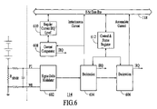
- FIG. 6 is a block diagram of an embodiment of a CC-ADC 114 .
- the CC-ADC 114 includes a sigma-delta modulator 602 , decimation filters 604 and 606 , a current comparator 608 , a regular current IRQ level 610 , a control and status register 612 and an 8-bit data bus 118 .
- the sigma-delta modulator 602 provides data to a decimation filter 604 .
- Decimation filter 604 provides data to decimation filter 606 , the current comparator 608 and the 8-bit databus 118 .
- the regular current IRQ level 610 receives data from the 8-bit databus 118 and provides data to the 8-bit databus 118 and the current comparator 608 .
- a control and status register 612 receives data from the 8-bit databus 118 , and provides data to decimation filters 604 and 606 .
- Decimation filter 606 receives data from the control and status register 612 and from decimation filter 604 , and provides data to the 8-bit databus 118 .
- Two different output values are provided: instantaneous current and accumulate current.
- the instantaneous current output has a short conversion time at the cost of lower resolution.
- the accumulate current output provides a highly accurate current measurement for Coulomb counting.
- the accumulate current output is a high-resolution, high accuracy output with programmable conversion time.
- the converted value is an accurate measurement of the average current flow during one conversion period.
- the CC-ADC 114 generates an interrupt each time a new accumulate current conversion has finished if the interrupt is enabled.
- the CPU 116 can enter sleep mode and wait for an interrupt from the accumulate current conversion. After adding the new accumulate current value for Coulomb Counting, the CPU 116 can go back to sleep again. This reduces the CPU workload, and allows more time spent in low power modes, reducing power consumption.
- the CC-ADC 114 can generate an interrupt if the result of an instantaneous current conversion is greater than a programmable threshold. This allows the detection of a regular current condition. This allows an ultra-low power operation, where the CC-ADC 114 can be configured to enter a regular current detection mode with a programmable current sampling interval. The CC-ADC 114 will repeatedly perform one instantaneous current conversion, before it is turned off for a timing interval specified by the user software. This allows operating the regular current detection while keeping the CC-ADC 114 off most of the time.
- FIG. 7 illustrates an embodiment of a low power band-gap voltage reference 112 in accordance with the present invention.
- the low power band-gap voltage reference 112 provides the microcontroller with an accurate on-chip reference voltage (V REF ) of 1.100V.
- V REF is used as reference for the on-chip voltage regulator 102 , the V-ADC 110 and the CC-ADC 114 ( FIG. 1 ).
- the reference to the two ADCs 110 and 114 uses a buffer 704 with external decoupling capacitor 706 to enable excellent noise performance with minimum power consumption.
- the reference voltage V REF — P /V REF — N to the CC-ADC 114 is scaled to match the full scale requirements at the current sense input pins. This configuration also enables concurrent operation of both V-ADC 110 and CC-ADC 114 .
- the microcontroller 100 includes a two-step calibration algorithm. This algorithm is described, for example, in the before-mentioned U.S. application Ser. No. 10/795,027.
- the first predetermined temperature such as 85°
- the second step is performed at a second predetermined temperature such as room temperature.
- the factory calibration is 85°
- the result is stored in the Flash memory.
- the second calibration step can be implemented by a user as an instruction in their test flow.
- the step requires an accurate input voltage and a stable room temperature.
- the calibration register can also be altered runtime to implement temperature compensation in software. Accuracy for any temperature inside the temperature range can be achieved.
- the microcontroller 100 includes an on-chip temperature sensor (not shown) for monitoring the die temperature.
- a voltage proportional-to-absolute temperature, V PTAT is generated in the voltage reference circuit and connected to the multiplexer at the V-ADC input.
- the temperature sensor can be used for runtime compensation of temperature drift in both the voltage reference and the on-chip oscillator 120 .
- FIG. 8 illustrates an embodiment of the battery protection CPU interface in accordance with the present invention.
- the battery protection CPU interface comprises current battery protection circuitry (CBPC) 804 and voltage battery protection circuitry (VBPC) 802 , and a plurality of battery protection parameter lockable registers 806 , 808 , 810 , 812 and 814 .
- the interface is coupled to the FET control 104 and the 8-bit data bus 118 .
- Each protection has an interrupt flag.
- Each flag can be read and cleared by the CPU 116 , and each flag has an individual interrupt enable. All enabled flags are combined into a single battery protection interrupt request to the CPU 116 . This interrupt can wake up the CPU 116 from any operation mode, except power-off. The interrupt flags are cleared by writing a logic ‘1’ to their bit locations from the CPU 116 .
- the over-current and short-circuit protection parameters are reprogrammable to adapt to different types of batteries.
- the parameters are set by writing to I/O registers.
- the parameter registers can be locked after the initial configuration, prohibiting any further updates until the next hardware reset.
- the battery protection parameters set in the battery protection parameter registers and the disable function set in the battery protection disable register can be locked from any further software updates. Once locked, these registers cannot be accessed until the next hardware reset. This provides a safe method for protecting these registers from unintentional modification by software runaway. It is recommended that software sets these registers shortly after reset, and then protects these registers from any further updates.
- the current battery protection circuitry (CBPC) 804 monitors the charge and discharge current and disables C-FET, PC-FET, and D-FET if an over-current or short-circuit condition is detected.
- CBPC current battery protection circuitry
- the external filter at the PI/NI input pins will cause too large delay for short-circuit detection. Therefore the separate PPI/NNI inputs are used for current battery protection.
- the application software After current battery protection has been activated, the application software must re-enable the FETs.
- the battery protection circuitry 106 provides a hold-off time of, for example, one second before software can re-enable the discharge FET. This provides safety in case the application software should unintentionally re-enable the discharge FET too
- the activation of a protection also issues an interrupt to the CPU 116 .
- the battery protection interrupts can be individually enabled and disabled by the CPU 116 .
- both short-circuit and discharge over-current protection are automatically deactivated when the D-FET is disabled.
- the charge over-current protection is disabled when both the C-FET and the PC-FET are disabled. Note however that charge over-current protection is never automatically disabled when any of the C-FET or PC-FETs are controlled by PWM.
- the deep under-voltage protection ensures that the battery cells will not be discharged deeper than the programmable deep under-voltage detection level. If the voltage at the VFET pin is below this level for a time longer than the programmable delay time, the FETs are automatically switched off and the microcontroller enters power-off mode.
- a deep under-voltage early warning interrupt flag (DUVIF) within the battery protection interrupt register will be set 250 ms before the microcontroller enters power-off. This will give the CPU 116 a chance to take necessary actions before the power is switched off.
- DVIF deep under-voltage early warning interrupt flag
- the microcontroller 100 will remain in the power-off mode until a charger is connected. When a charger is detected, a normal power-up sequence is started and the microcontroller 100 initializes to default state.
- the deep under-voltage delay time and deep under-voltage detection level are set in the battery protection deep under-voltage register (BPDUV) which is part of the battery protection level register.
- the parameter registers can be locked after the initial configuration, prohibiting any further updates until the next hardware reset.
- the current battery protection current monitors the cell current by sampling the voltage at the PPI/NNI input pins.
- a differential operational amplifier amplifies the voltage with a suitable gain.
- the output from the operational amplifier is compared to an accurate, programmable on-chip voltage reference by an analog comparator. If the shunt resistor voltage is above the discharge over-current detection level for a time longer than over-current protection reaction time, the microcontroller 100 activates discharge over-current protection.
- a sampled system clocked by an internal ULP oscillator is used for over-current and short-circuit protection. This ensures a reliable clock source, off-set cancellation and low power consumption.
- the external D-FET, PC-FET, and C-FET are disabled and a current protection timer is started. This timer ensures that the FETs are disabled for a predetermined period of time (i.e., one second).
- the application software must then set the DFE and CFE bits in the FET control and status register to re-enable normal operation when this is considered safe. If the D-FET is re-enabled while the loading of the battery still is too large, the discharge over-current protection will be activated again.
- the microcontroller 100 activates charge over-current protection.
- the external D-FET, PC-FET, and C-FET are disabled and a current protection timer is started. This timer ensures that the FETs are disabled for at least one second.
- the DFE and CFE bits in the FET control and status register 302 ( FIG. 3 ) are set to re-enable normal operation when this is considered safe. If the C-FET is re-enabled and the charger continues to supply too high of a current, the charge over-current protection will be activated again.
- a second level of high current detection is provided to enable a faster response time to very large discharge currents. If a discharge current larger than the short-circuit detection level is present for a period longer than short-circuit reaction time, the short-circuit protection is activated.
- the D-FET, PC-FET, and C-FET are disabled and a current protection timer is started. This timer ensures that the D-FET, PC-FET, and C-FET are disabled for at least one second.
- the application software must then set the DFE and CFE bits in the FET control and status register 302 ( FIG. 3 ) to re-enable normal operation when this is considered safe. If the D-FET is re-enabled before the cause of the short-circuit condition is removed, the short-circuit protection will be activated again.
- the microcontroller 100 features various low-power modes called sleep modes. Sleep modes enable the application to shut down unused modules in the microcontroller 100 , thereby saving power.
- the microcontroller 100 provides four sleep modes allowing the user to tailor the power consumption to the application's requirement:
- Idle mode in which the CPU 116 is stopped but all peripheral functions continue operating.
- ADC noise reduction mode which improves the noise environment for the ADC while saving power. If the V-ADC 110 ( FIG. 1 ) is enabled, a conversion starts automatically once this mode is entered.
- Power-off mode enables the voltage regulator 102 ( FIG. 1 ) to shut off power to the CPU 116 , leaving only the voltage regulator 102 and the charger detect circuitry 128 to be operational. In this mode the microcontroller 100 ensures that the battery cells are not damaged if the voltage is too low.
- a system and method in accordance with the present invention provides for a microcontroller which includes battery management and protection.
- the microcontroller provides for a single chip device which includes battery protection and management. This one-chip solution saves design cost and PCB space in addition to broadening the functionality of the smart battery application. With the accuracy of the microcontroller, the charge status of the battery can be predicted more accurately and therefore effectively increases actual battery capacity.
Abstract
Description
-
- Input to voltage regulator. This input provides power to the device drawn directly from the battery, in the range of 4-25 volts.
- Input to voltage ADC for individual cell voltage measurements.
- Input to detect the presence of a battery charger.
-
- Outputs to charge, discharge, and pre-charge FETs.
-
- Simple but powerful and flexible communication interface, only two bus lines needed
- Both master and slave operation supported
- Device can operate as transmitter or receiver
- 7-bit address space allows up to 128 different slave addresses
- Multi-master arbitration support
- Operates on 4 MHz clock, achieving up to 100 kHz data transfer speed
- Slew-rate limited output drivers
- Noise suppression circuitry rejects spikes on bus lines
- Fully programmable slave address with general call support
- Address recognition causes wake-up when the CPU is in sleep mode
| TABLE 1 |
| Effect of Battery Protection Types |
| Battery | Cell | |||||
| Protection | Interrupt | Balancing | ||||
| Type | Requests | C-FET | D-FET | PC-FET | FETs | MCU |
| Deep under- | CPU Reset on exit | Disabled | Disabled | Disabled | Disabled | Power-off |
| voltage detected | ||||||
| Discharge over- | Entry and exit | Disabled | Disabled | Disabled | Operational | Operational |
| current protection | ||||||
| Charge over- | Entry and exit | Disabled | Disabled | Disabled | Operational | Operational |
| current protection | ||||||
| Short-circuit protection | Entry and exit | Disabled | Disabled | Disabled | Operational | Operational |
| Condition | Current Draw | ||
| Active 1 MHz | 1.2 | mA | ||
| Idle 1 MHz | 0.6 | mA | ||
| Power-save | 90 | μA | ||
| Power-down | 20 | μA | ||
| Power-off | 2 | μA | ||
Claims (21)
Priority Applications (8)
| Application Number | Priority Date | Filing Date | Title |
|---|---|---|---|
| US11/335,057 US7759902B2 (en) | 2005-01-19 | 2006-01-18 | Single chip microcontroller including battery management and protection |
| CN200680002538XA CN101233663B (en) | 2005-01-19 | 2006-01-19 | Single chip microcontroller including battery management and protection |
| EP06718949.8A EP1842273A4 (en) | 2005-01-19 | 2006-01-19 | Single chip microcontroller including battery management and protection |
| TW095102016A TWI345707B (en) | 2005-01-19 | 2006-01-19 | Single chip microcontroller including battery management and protection |
| PCT/US2006/001951 WO2006078850A2 (en) | 2005-01-19 | 2006-01-19 | Single chip microcontroller including battery management and protection |
| NO20074247A NO20074247L (en) | 2005-01-19 | 2007-08-20 | Single chip microcontroller including battery management and protection |
| HK08112888.2A HK1119840A1 (en) | 2005-01-19 | 2008-11-25 | Single chip microcontroller including battery management and protection |
| US12/839,249 US8143860B2 (en) | 2005-01-19 | 2010-07-19 | Single chip microcontroller including battery management and protection |
Applications Claiming Priority (2)
| Application Number | Priority Date | Filing Date | Title |
|---|---|---|---|
| US64546005P | 2005-01-19 | 2005-01-19 | |
| US11/335,057 US7759902B2 (en) | 2005-01-19 | 2006-01-18 | Single chip microcontroller including battery management and protection |
Related Child Applications (1)
| Application Number | Title | Priority Date | Filing Date |
|---|---|---|---|
| US12/839,249 Continuation US8143860B2 (en) | 2005-01-19 | 2010-07-19 | Single chip microcontroller including battery management and protection |
Publications (2)
| Publication Number | Publication Date |
|---|---|
| US20060170398A1 US20060170398A1 (en) | 2006-08-03 |
| US7759902B2 true US7759902B2 (en) | 2010-07-20 |
Family
ID=36692882
Family Applications (2)
| Application Number | Title | Priority Date | Filing Date |
|---|---|---|---|
| US11/335,057 Active 2026-02-14 US7759902B2 (en) | 2005-01-19 | 2006-01-18 | Single chip microcontroller including battery management and protection |
| US12/839,249 Active US8143860B2 (en) | 2005-01-19 | 2010-07-19 | Single chip microcontroller including battery management and protection |
Family Applications After (1)
| Application Number | Title | Priority Date | Filing Date |
|---|---|---|---|
| US12/839,249 Active US8143860B2 (en) | 2005-01-19 | 2010-07-19 | Single chip microcontroller including battery management and protection |
Country Status (6)
| Country | Link |
|---|---|
| US (2) | US7759902B2 (en) |
| EP (1) | EP1842273A4 (en) |
| HK (1) | HK1119840A1 (en) |
| NO (1) | NO20074247L (en) |
| TW (1) | TWI345707B (en) |
| WO (1) | WO2006078850A2 (en) |
Cited By (14)
| Publication number | Priority date | Publication date | Assignee | Title |
|---|---|---|---|---|
| US20090021222A1 (en) * | 2007-07-19 | 2009-01-22 | Hitachi Vehicle Energy, Ltd. | Cell controller |
| US20100176787A1 (en) * | 2009-01-13 | 2010-07-15 | Nuvoton Technology Corporation | Power converter |
| US8143860B2 (en) | 2005-01-19 | 2012-03-27 | Atmel Corporation | Single chip microcontroller including battery management and protection |
| US20120246504A1 (en) * | 2011-03-24 | 2012-09-27 | Hon Hai Precision Industry Co., Ltd. | Electronic device for detecting a type of a charger device during a sleep mode |
| US20120256540A1 (en) * | 2009-12-22 | 2012-10-11 | Ritelite (Systems) Limited | Led lighting apparatus with a battery monitoring device |
| US20130265059A1 (en) * | 2010-10-08 | 2013-10-10 | A123 Systems, Inc. | System and Method for Verifying a Reference Voltage for Battery Cell Monitoring |
| US20140055082A1 (en) * | 2012-08-23 | 2014-02-27 | Qualcomm Incorporated | Charging current calibration |
| US20140281277A1 (en) * | 2013-03-15 | 2014-09-18 | Seagate Technology Llc | Integrated system and storage media controlller |
| CN104659852A (en) * | 2013-11-21 | 2015-05-27 | 联创汽车电子有限公司 | Battery management system of electromobile |
| US9564761B2 (en) * | 2014-11-21 | 2017-02-07 | Palladium Energy, Inc. | Conformable wearable battery with removable command module |
| US20170207642A1 (en) * | 2016-01-15 | 2017-07-20 | Renesas Electronics America Inc. | E-fuse/switch by back end of line (beol) process |
| US20180205239A1 (en) * | 2017-01-17 | 2018-07-19 | Taiyo Yuden Co., Ltd. | Power supply module with lithium ion capacitor |
| US11604229B2 (en) | 2020-12-28 | 2023-03-14 | Analog Devices International Unlimited Company | Techniques for determining energy storage device state of health |
| US11835584B2 (en) | 2020-08-19 | 2023-12-05 | Analog Devices International Unlimited Company | Battery SOH determination circuit |
Families Citing this family (44)
| Publication number | Priority date | Publication date | Assignee | Title |
|---|---|---|---|---|
| TW200627784A (en) * | 2005-01-17 | 2006-08-01 | Holtek Semiconductor Inc | Temperature compensation circuit and method |
| US7629769B2 (en) * | 2006-03-10 | 2009-12-08 | Atmel Corporation | Power surge filtering in over-current and short circuit protection |
| US7561901B2 (en) * | 2006-05-15 | 2009-07-14 | Telefonaktiebolaget Lm Ericsson (Publ) | Adaptation of push mail filters to save UE battery power |
| TWI397807B (en) * | 2009-02-23 | 2013-06-01 | Novatek Microelectronics Corp | Energy-efficient touch panel device and related method |
| US9001071B2 (en) | 2009-02-23 | 2015-04-07 | Novatek Microelectronics Corp. | Energy-efficient touch panel device and related method |
| US20120109248A1 (en) * | 2009-07-10 | 2012-05-03 | Therese Danielsson | Battery discharge measurement device and method |
| US8604754B2 (en) | 2009-09-10 | 2013-12-10 | Ivus Industries, Llc | Universal power interface bus |
| TW201112577A (en) * | 2009-09-29 | 2011-04-01 | jin-cheng Gao | Power supply device capable of detecting load rated voltage automatically and its method |
| EP2488926B1 (en) * | 2009-10-14 | 2013-08-07 | Energy Micro AS | Low power reference |
| TWI394972B (en) * | 2009-11-25 | 2013-05-01 | Htc Corp | Method and system for estimating battery percentage |
| KR101057542B1 (en) | 2010-01-26 | 2011-08-17 | 에스비리모티브 주식회사 | Battery Management System and Its Driving Method |
| US9136717B2 (en) * | 2010-03-26 | 2015-09-15 | Semiconductor Components Industries, Llc | Semiconductor integrated circuit |
| US8015452B2 (en) * | 2010-08-31 | 2011-09-06 | O2Micro International, Ltd. | Flexible bus architecture for monitoring and control of battery pack |
| DE102010040721A1 (en) * | 2010-09-14 | 2012-03-15 | Sb Limotive Company Ltd. | Battery system with cell voltage detection units |
| US20120166918A1 (en) * | 2010-12-22 | 2012-06-28 | Atmel Corporation | Verification of Configuration Parameters |
| US9054528B2 (en) | 2010-12-22 | 2015-06-09 | Atmel Corporation | Event system and timekeeping for battery management and protection system |
| US8843538B2 (en) | 2010-12-22 | 2014-09-23 | Atmel Corporation | Measuring sum of squared current |
| US8943335B2 (en) * | 2010-12-22 | 2015-01-27 | Atmel Corporation | Battery management and protection system using a module in a sleepwalking mode to monitor operational characteristics of a battery |
| JP2012208922A (en) * | 2011-03-17 | 2012-10-25 | Ricoh Co Ltd | Information processor, power-saving control method, program, and recording medium |
| JP5659967B2 (en) | 2011-06-24 | 2015-01-28 | ソニー株式会社 | Monitoring device |
| DE102011085787A1 (en) * | 2011-11-04 | 2013-05-08 | Sb Limotive Company Ltd. | Battery management unit with a variety of monitoring IC chips |
| WO2013079982A1 (en) * | 2011-12-02 | 2013-06-06 | Rimac Automobil D.O.O. | Battery management system for starter 12/24v battery cells, particularly cells from new generation of lithium-ionic or lithium-ferrous-phosphate batteries |
| JP5870763B2 (en) * | 2012-03-02 | 2016-03-01 | ミツミ電機株式会社 | Secondary battery monitoring device and battery pack |
| US9007067B2 (en) * | 2012-08-28 | 2015-04-14 | Energy Pass Incorporation | Apparatus and method for estimating battery condition of battery pack by solely monitoring one selected battery cell |
| US9236752B2 (en) * | 2012-09-07 | 2016-01-12 | Qualcomm Incorporated | Method and system for voltage collapse protection |
| US20140333287A1 (en) * | 2013-05-10 | 2014-11-13 | Sunny GUPTA | System for measuring power consumption of integrated circuit |
| WO2014204649A1 (en) * | 2013-06-18 | 2014-12-24 | Rocketship, Inc. | Battery management system |
| US20150029398A1 (en) * | 2013-07-24 | 2015-01-29 | Kabushiki Kaisha Toshiba | Information processing apparatus and information processing method for outputting a charging status |
| WO2015113466A1 (en) | 2014-01-28 | 2015-08-06 | 广东欧珀移动通信有限公司 | Power adapter, terminal, and method for processing exception of charging loop |
| CN103762691B (en) | 2014-01-28 | 2015-12-23 | 广东欧珀移动通信有限公司 | Battery charger and cell charge protection control method |
| TWI545863B (en) | 2014-05-21 | 2016-08-11 | 廣達電腦股份有限公司 | Battery protection system and battery protection method |
| JP5888387B1 (en) * | 2014-10-22 | 2016-03-22 | ミツミ電機株式会社 | Battery protection circuit, battery protection device, and battery pack |
| TWI576596B (en) * | 2014-11-20 | 2017-04-01 | 力智電子股份有限公司 | Electric capacity measurement apparatus with temperature compensation and temperature compensation method thereof |
| US10141754B2 (en) | 2015-05-21 | 2018-11-27 | Robert Bosch Gmbh | Integration of battery management system and battery charger |
| CN106058963A (en) * | 2016-06-01 | 2016-10-26 | 佛山华平勇创能源科技有限公司 | Lithium cell capacity tracking monitor system |
| TWI583096B (en) * | 2016-06-16 | 2017-05-11 | 盧昭正 | Cell charge protection device |
| US10367234B2 (en) | 2016-08-22 | 2019-07-30 | Microsoft Technology Licensing, Llc | Battery having integrated safety controller and power management controller |
| TWI646802B (en) * | 2017-12-26 | 2019-01-01 | 國家中山科學研究院 | Battery system control network and reset method thereof |
| CN207801530U (en) * | 2018-01-17 | 2018-08-31 | 创科(澳门离岸商业服务)有限公司 | Battery management system |
| DE102018221856A1 (en) * | 2018-12-17 | 2020-06-18 | Robert Bosch Gmbh | Battery module for a motor vehicle |
| US11070068B2 (en) | 2019-02-06 | 2021-07-20 | International Business Machines Corporation | Battery pack and method for discharging the same after a fault event |
| US10742242B1 (en) | 2019-06-05 | 2020-08-11 | Silicon Laboratories Inc. | Apparatus for improving the effective performance of a power source and associated methods |
| CN112397799A (en) * | 2020-12-08 | 2021-02-23 | 北京绿能芯创电子科技有限公司 | Battery management metering method and system |
| CN112713858A (en) * | 2020-12-22 | 2021-04-27 | 上海东软载波微电子有限公司 | Oscillator |
Citations (26)
| Publication number | Priority date | Publication date | Assignee | Title |
|---|---|---|---|---|
| US4553081A (en) * | 1982-06-07 | 1985-11-12 | Norand Corporation | Portable battery powered system |
| US5278487A (en) | 1988-03-15 | 1994-01-11 | Norand Corporation | Battery conditioning system having communication with battery parameter memory means in conjunction with battery conditioning |
| US5357203A (en) * | 1992-07-08 | 1994-10-18 | Benchmarq Microelectronics, Inc. | Battery monitoring circuit for operating with high battery discharge rates |
| US5408235A (en) | 1994-03-07 | 1995-04-18 | Intel Corporation | Second order Sigma-Delta based analog to digital converter having superior analog components and having a programmable comb filter coupled to the digital signal processor |
| US5479085A (en) * | 1992-11-27 | 1995-12-26 | Honda Giken Kogyo Kabushiki Kaisha | Method and apparatus for measuring residual capacity of an electric-vehicle battery |
| US5619430A (en) * | 1995-10-10 | 1997-04-08 | Microchip Technology Inc. | Microcontroller with on-chip linear temperature sensor |
| US5909188A (en) | 1997-02-24 | 1999-06-01 | Rosemont Inc. | Process control transmitter with adaptive analog-to-digital converter |
| US5955869A (en) * | 1996-07-17 | 1999-09-21 | Rathmann; Roland | Battery pack and a method for monitoring remaining capacity of a battery pack |
| US6081216A (en) | 1998-06-11 | 2000-06-27 | Motorola, Inc. | Low-power decimator for an oversampled analog-to-digital converter and method therefor |
| US6218809B1 (en) | 1998-03-20 | 2001-04-17 | Dallas Semiconductor Corporation | Method for monitoring operating parameters of a rechargeable power supply |
| US6456219B1 (en) | 2000-02-22 | 2002-09-24 | Texas Instruments Incorporated | Analog-to-digital converter including two-wire interface circuit |
| US6489749B1 (en) * | 1999-08-05 | 2002-12-03 | Seiko Instruments Inc. | Battery state monitoring circuit having differentiating circuit |
| US6507171B2 (en) | 2000-12-29 | 2003-01-14 | Nokia Corporation | Method and apparatus for measuring battery charge and discharge current using a direct analog-to-digital conversion of a charge/discharge replica current |
| US6580250B1 (en) * | 2002-02-28 | 2003-06-17 | Dialog Semiconductor Gmbh | Monolithic battery protection circuit |
| US6614374B1 (en) | 1999-06-15 | 2003-09-02 | Globespanvirata, Inc. | High performance switched-capacitor filter for oversampling Sigma-Delta digital to analog converters |
| US6646845B1 (en) * | 2000-09-21 | 2003-11-11 | Delphi Technologies, Inc. | Battery protection system and method |
| US20050062457A1 (en) | 2003-09-18 | 2005-03-24 | Texas Instruments Incorporated | Battery charger interface architecture suitable for digital process |
| US6898534B2 (en) | 2003-05-05 | 2005-05-24 | Texas Instruments Incorporated | DC measurement method and system using sigma-delta modulation pattern |
| US20050127879A1 (en) * | 2003-11-14 | 2005-06-16 | Hideyuki Sato | Battery pack, battery protection processing apparatus, and startup control method of the battery protection processing apparatus |
| US20050197795A1 (en) | 2004-03-04 | 2005-09-08 | Arne Aas | Method and apparatus of temperature compensation for integrated circuit chip using on-chip sensor and computation means |
| US20050212489A1 (en) * | 2004-03-25 | 2005-09-29 | Denning Bruce S | Over voltage transient controller |
| US20050242779A1 (en) * | 2003-11-21 | 2005-11-03 | Katsura Yoshio | Battery protection circuit |
| US20050269992A1 (en) * | 2004-06-03 | 2005-12-08 | Zheren Lai | Over voltage and over current protection integrated circuit |
| US20060071643A1 (en) * | 2004-10-04 | 2006-04-06 | Carrier David A | Method and device for monitoring battery cells of a battery pack and method and arrangement for balancing battery cell voltages during charge |
| WO2006078850A2 (en) | 2005-01-19 | 2006-07-27 | Atmel Corporation | Single chip microcontroller including battery management and protection |
| US7113122B2 (en) | 2005-01-19 | 2006-09-26 | Atmel Corporation | Current sensing analog to digital converter and method of use |
Family Cites Families (16)
| Publication number | Priority date | Publication date | Assignee | Title |
|---|---|---|---|---|
| US689534A (en) * | 1901-08-22 | 1901-12-24 | John J Bloom | Garment-supporter. |
| US5539298A (en) * | 1993-03-19 | 1996-07-23 | Compaq Computer Corporation | Pulse charge technique to trickle charge a rechargeable battery |
| US5355869A (en) * | 1994-02-15 | 1994-10-18 | The United States Of America As Represented By The Secretary Of The Army | Self-heating group meal assembly and method of using same |
| TW231373B (en) | 1994-02-17 | 1994-10-01 | United Microelectronics Corp | Fabricating method for EEPROM IC with MONOS/MNOS structrue |
| FI945943A (en) | 1994-12-16 | 1996-06-17 | Abb Industry Oy | Input circuit for both analog and digital signals |
| JP2865026B2 (en) | 1995-06-30 | 1999-03-08 | 日本電気株式会社 | Comparator |
| US5774733A (en) * | 1995-10-03 | 1998-06-30 | Microchip Technology Incorporated | Microcontroller with analog front-end for providing intelligent battery management |
| US5903764A (en) | 1997-05-02 | 1999-05-11 | Micro International, Ltd. | Smart battery selector offering power conversion internally within a portable device |
| US6252511B1 (en) | 1997-06-20 | 2001-06-26 | Compaq Computer Corporation | Real-time battery gauge display |
| JP3105862B2 (en) | 1998-02-27 | 2000-11-06 | 日本電気株式会社 | Voltage comparison circuit |
| US6065122A (en) | 1998-03-13 | 2000-05-16 | Compaq Computer Corporation | Smart battery power management in a computer system |
| US6215337B1 (en) | 1999-01-12 | 2001-04-10 | Qualcomm Incorporated | Linear sampling switch |
| US6898537B1 (en) * | 2001-04-27 | 2005-05-24 | Nanometrics Incorporated | Measurement of diffracting structures using one-half of the non-zero diffracted orders |
| JP3497495B2 (en) | 2001-11-21 | 2004-02-16 | 株式会社半導体理工学研究センター | Sample hold circuit |
| TW530429B (en) | 2001-12-24 | 2003-05-01 | Avid Electronics Corp | Intelligent secondary battery management method and device |
| US7167029B2 (en) | 2005-01-19 | 2007-01-23 | Atmel Corporation | Sampling and level shifting circuit |
-
2006
- 2006-01-18 US US11/335,057 patent/US7759902B2/en active Active
- 2006-01-19 WO PCT/US2006/001951 patent/WO2006078850A2/en active Application Filing
- 2006-01-19 TW TW095102016A patent/TWI345707B/en active
- 2006-01-19 EP EP06718949.8A patent/EP1842273A4/en not_active Withdrawn
-
2007
- 2007-08-20 NO NO20074247A patent/NO20074247L/en not_active Application Discontinuation
-
2008
- 2008-11-25 HK HK08112888.2A patent/HK1119840A1/en not_active IP Right Cessation
-
2010
- 2010-07-19 US US12/839,249 patent/US8143860B2/en active Active
Patent Citations (27)
| Publication number | Priority date | Publication date | Assignee | Title |
|---|---|---|---|---|
| US4553081A (en) * | 1982-06-07 | 1985-11-12 | Norand Corporation | Portable battery powered system |
| US5278487A (en) | 1988-03-15 | 1994-01-11 | Norand Corporation | Battery conditioning system having communication with battery parameter memory means in conjunction with battery conditioning |
| US5357203A (en) * | 1992-07-08 | 1994-10-18 | Benchmarq Microelectronics, Inc. | Battery monitoring circuit for operating with high battery discharge rates |
| US5479085A (en) * | 1992-11-27 | 1995-12-26 | Honda Giken Kogyo Kabushiki Kaisha | Method and apparatus for measuring residual capacity of an electric-vehicle battery |
| US5408235A (en) | 1994-03-07 | 1995-04-18 | Intel Corporation | Second order Sigma-Delta based analog to digital converter having superior analog components and having a programmable comb filter coupled to the digital signal processor |
| US5619430A (en) * | 1995-10-10 | 1997-04-08 | Microchip Technology Inc. | Microcontroller with on-chip linear temperature sensor |
| US5955869A (en) * | 1996-07-17 | 1999-09-21 | Rathmann; Roland | Battery pack and a method for monitoring remaining capacity of a battery pack |
| US5909188A (en) | 1997-02-24 | 1999-06-01 | Rosemont Inc. | Process control transmitter with adaptive analog-to-digital converter |
| US6218809B1 (en) | 1998-03-20 | 2001-04-17 | Dallas Semiconductor Corporation | Method for monitoring operating parameters of a rechargeable power supply |
| US6081216A (en) | 1998-06-11 | 2000-06-27 | Motorola, Inc. | Low-power decimator for an oversampled analog-to-digital converter and method therefor |
| US6614374B1 (en) | 1999-06-15 | 2003-09-02 | Globespanvirata, Inc. | High performance switched-capacitor filter for oversampling Sigma-Delta digital to analog converters |
| US6489749B1 (en) * | 1999-08-05 | 2002-12-03 | Seiko Instruments Inc. | Battery state monitoring circuit having differentiating circuit |
| US6456219B1 (en) | 2000-02-22 | 2002-09-24 | Texas Instruments Incorporated | Analog-to-digital converter including two-wire interface circuit |
| US6646845B1 (en) * | 2000-09-21 | 2003-11-11 | Delphi Technologies, Inc. | Battery protection system and method |
| US6507171B2 (en) | 2000-12-29 | 2003-01-14 | Nokia Corporation | Method and apparatus for measuring battery charge and discharge current using a direct analog-to-digital conversion of a charge/discharge replica current |
| US6580250B1 (en) * | 2002-02-28 | 2003-06-17 | Dialog Semiconductor Gmbh | Monolithic battery protection circuit |
| US6898534B2 (en) | 2003-05-05 | 2005-05-24 | Texas Instruments Incorporated | DC measurement method and system using sigma-delta modulation pattern |
| US20050062457A1 (en) | 2003-09-18 | 2005-03-24 | Texas Instruments Incorporated | Battery charger interface architecture suitable for digital process |
| US20050127879A1 (en) * | 2003-11-14 | 2005-06-16 | Hideyuki Sato | Battery pack, battery protection processing apparatus, and startup control method of the battery protection processing apparatus |
| US20050242779A1 (en) * | 2003-11-21 | 2005-11-03 | Katsura Yoshio | Battery protection circuit |
| US20050197795A1 (en) | 2004-03-04 | 2005-09-08 | Arne Aas | Method and apparatus of temperature compensation for integrated circuit chip using on-chip sensor and computation means |
| US20050212489A1 (en) * | 2004-03-25 | 2005-09-29 | Denning Bruce S | Over voltage transient controller |
| US20050269992A1 (en) * | 2004-06-03 | 2005-12-08 | Zheren Lai | Over voltage and over current protection integrated circuit |
| US20060071643A1 (en) * | 2004-10-04 | 2006-04-06 | Carrier David A | Method and device for monitoring battery cells of a battery pack and method and arrangement for balancing battery cell voltages during charge |
| WO2006078850A2 (en) | 2005-01-19 | 2006-07-27 | Atmel Corporation | Single chip microcontroller including battery management and protection |
| US7113122B2 (en) | 2005-01-19 | 2006-09-26 | Atmel Corporation | Current sensing analog to digital converter and method of use |
| US7292174B2 (en) | 2005-01-19 | 2007-11-06 | Atmel Corporation | Current sensing analog to digital converter and method of use |
Non-Patent Citations (6)
| Title |
|---|
| "International Application Serial No. PCT/US2006/001951, Search Report mailed Aug. 17, 2007". |
| Barsukov, et al., "Fuel Gauge Technology Predicts Run Time in Multi-Cell Portable Applications", http://www.ednasia.com/print.asp?id=108, 5 pgs. |
| Barsukov, Yevgen et al.; email; RE: Fuel Gauge Technology Predicts Run Time in Multi-Cell Portable Applications, Texas Instruments; available @ www.ednasia.com/article.asp?id=108; last accessed Jan. 13, 2005; 5 pgs. |
| Davis, J., "TI Improves Battery Gauge", http://www.reed-electronics.com/electronicnews, (Sep. 13, 2004), 1 pg. |
| Davis, Jessica; email; RE: TI Improves Battery Gauge; Electronic News; available @ www.reed-electronics.com/electronicnews/index.asp?layout=articlePrint&articleID=CA452 . . . ; last accessed Jan. 17, 2005, 1 pg. |
| Gangsto, Gunnar et al., "Current Sensing Analog to Digital Converter and Method of Use," U.S. Appl. No. 11/043,669, filed Jan. 25, 2005, 50 pgs. |
Cited By (21)
| Publication number | Priority date | Publication date | Assignee | Title |
|---|---|---|---|---|
| US8143860B2 (en) | 2005-01-19 | 2012-03-27 | Atmel Corporation | Single chip microcontroller including battery management and protection |
| US8487590B2 (en) * | 2007-07-19 | 2013-07-16 | Hitachi Vehicle Energy, Ltd | Cell controller having a unit cell voltage detecting section |
| US20090021222A1 (en) * | 2007-07-19 | 2009-01-22 | Hitachi Vehicle Energy, Ltd. | Cell controller |
| US20100176787A1 (en) * | 2009-01-13 | 2010-07-15 | Nuvoton Technology Corporation | Power converter |
| US7932708B2 (en) * | 2009-01-13 | 2011-04-26 | Nuvoton Technology Corporation | Power converter |
| US20120256540A1 (en) * | 2009-12-22 | 2012-10-11 | Ritelite (Systems) Limited | Led lighting apparatus with a battery monitoring device |
| US9618544B2 (en) * | 2010-10-08 | 2017-04-11 | A123 Systems Llc | System and method for verifying a reference voltage for battery cell monitoring |
| US20130265059A1 (en) * | 2010-10-08 | 2013-10-10 | A123 Systems, Inc. | System and Method for Verifying a Reference Voltage for Battery Cell Monitoring |
| US20120246504A1 (en) * | 2011-03-24 | 2012-09-27 | Hon Hai Precision Industry Co., Ltd. | Electronic device for detecting a type of a charger device during a sleep mode |
| US8539273B2 (en) * | 2011-03-24 | 2013-09-17 | Hon Hai Precision Industry Co., Ltd. | Electronic device for detecting a type of a charger device during a sleep mode |
| US20140055082A1 (en) * | 2012-08-23 | 2014-02-27 | Qualcomm Incorporated | Charging current calibration |
| US9190862B2 (en) * | 2012-08-23 | 2015-11-17 | Qualcomm Incorporated | Charging current calibration |
| US20140281277A1 (en) * | 2013-03-15 | 2014-09-18 | Seagate Technology Llc | Integrated system and storage media controlller |
| US10031864B2 (en) * | 2013-03-15 | 2018-07-24 | Seagate Technology Llc | Integrated circuit |
| CN104659852B (en) * | 2013-11-21 | 2017-02-01 | 联创汽车电子有限公司 | Battery management system of electromobile |
| CN104659852A (en) * | 2013-11-21 | 2015-05-27 | 联创汽车电子有限公司 | Battery management system of electromobile |
| US9564761B2 (en) * | 2014-11-21 | 2017-02-07 | Palladium Energy, Inc. | Conformable wearable battery with removable command module |
| US20170207642A1 (en) * | 2016-01-15 | 2017-07-20 | Renesas Electronics America Inc. | E-fuse/switch by back end of line (beol) process |
| US20180205239A1 (en) * | 2017-01-17 | 2018-07-19 | Taiyo Yuden Co., Ltd. | Power supply module with lithium ion capacitor |
| US11835584B2 (en) | 2020-08-19 | 2023-12-05 | Analog Devices International Unlimited Company | Battery SOH determination circuit |
| US11604229B2 (en) | 2020-12-28 | 2023-03-14 | Analog Devices International Unlimited Company | Techniques for determining energy storage device state of health |
Also Published As
| Publication number | Publication date |
|---|---|
| EP1842273A4 (en) | 2015-03-25 |
| US20100287389A1 (en) | 2010-11-11 |
| WO2006078850A2 (en) | 2006-07-27 |
| US20060170398A1 (en) | 2006-08-03 |
| WO2006078850A3 (en) | 2007-10-18 |
| TW200634526A (en) | 2006-10-01 |
| TWI345707B (en) | 2011-07-21 |
| US8143860B2 (en) | 2012-03-27 |
| EP1842273A2 (en) | 2007-10-10 |
| HK1119840A1 (en) | 2009-03-13 |
| NO20074247L (en) | 2007-08-20 |
Similar Documents
| Publication | Publication Date | Title |
|---|---|---|
| US7759902B2 (en) | Single chip microcontroller including battery management and protection | |
| CN101233663B (en) | Single chip microcontroller including battery management and protection | |
| US8943335B2 (en) | Battery management and protection system using a module in a sleepwalking mode to monitor operational characteristics of a battery | |
| US10431976B2 (en) | Mechanism to extend the peak power capability of a mobile platform | |
| US5136231A (en) | Ni-cad battery charge rate controller | |
| US7629769B2 (en) | Power surge filtering in over-current and short circuit protection | |
| US6897635B2 (en) | Method for predicting remaining charge of portable electronics battery | |
| US8957639B2 (en) | Event system and timekeeping for battery management and protection system | |
| US7293188B2 (en) | Low voltage detection system | |
| JP3718769B2 (en) | Intelligent battery | |
| JP2002222031A (en) | Information processor and power consumption control method for the same processor | |
| US20120032645A1 (en) | Battery pack for practical low-power mode current detection and method of detecting excessive current | |
| JP2001054242A (en) | Battery condition monitoring circuit and battery apparatus | |
| US20060132093A1 (en) | Battery pack leakage cut-off | |
| EP4016789A1 (en) | Battery management apparatus | |
| US20120161746A1 (en) | Low-power operation for devices with circuitry for providing reference or regulated voltages | |
| JP5279762B2 (en) | Electronic device capable of reducing power consumption in power-off state and method for reducing power consumption | |
| US20210311540A1 (en) | Power-saving power architecture for integrated circuits such as microcontrollers | |
| US8030896B2 (en) | Multi-output voltage battery module and electronic device using the same | |
| JP6759200B2 (en) | Battery pack and secondary battery discharge control method | |
| TWI836705B (en) | Power system | |
| CN112868158A (en) | Charging device and charging method |
Legal Events
| Date | Code | Title | Description |
|---|---|---|---|
| AS | Assignment |
Owner name: ATMEL CORPORATION, CALIFORNIA Free format text: ASSIGNMENT OF ASSIGNORS INTEREST;ASSIGNORS:GANGSTO, GUNNAR;AAS, ARNE;SORASEN, RUNAR;REEL/FRAME:017770/0400 Effective date: 20060310 |
|
| FEPP | Fee payment procedure |
Free format text: PAYOR NUMBER ASSIGNED (ORIGINAL EVENT CODE: ASPN); ENTITY STATUS OF PATENT OWNER: LARGE ENTITY |
|
| STCF | Information on status: patent grant |
Free format text: PATENTED CASE |
|
| CC | Certificate of correction | ||
| FPAY | Fee payment |
Year of fee payment: 4 |
|
| AS | Assignment |
Owner name: MORGAN STANLEY SENIOR FUNDING, INC. AS ADMINISTRATIVE AGENT, NEW YORK Free format text: PATENT SECURITY AGREEMENT;ASSIGNOR:ATMEL CORPORATION;REEL/FRAME:031912/0173 Effective date: 20131206 Owner name: MORGAN STANLEY SENIOR FUNDING, INC. AS ADMINISTRAT Free format text: PATENT SECURITY AGREEMENT;ASSIGNOR:ATMEL CORPORATION;REEL/FRAME:031912/0173 Effective date: 20131206 |
|
| AS | Assignment |
Owner name: ATMEL CORPORATION, CALIFORNIA Free format text: TERMINATION AND RELEASE OF SECURITY INTEREST IN PATENT COLLATERAL;ASSIGNOR:MORGAN STANLEY SENIOR FUNDING, INC.;REEL/FRAME:038376/0001 Effective date: 20160404 |
|
| AS | Assignment |
Owner name: JPMORGAN CHASE BANK, N.A., AS ADMINISTRATIVE AGENT, ILLINOIS Free format text: SECURITY INTEREST;ASSIGNOR:ATMEL CORPORATION;REEL/FRAME:041715/0747 Effective date: 20170208 Owner name: JPMORGAN CHASE BANK, N.A., AS ADMINISTRATIVE AGENT Free format text: SECURITY INTEREST;ASSIGNOR:ATMEL CORPORATION;REEL/FRAME:041715/0747 Effective date: 20170208 |
|
| MAFP | Maintenance fee payment |
Free format text: PAYMENT OF MAINTENANCE FEE, 8TH YEAR, LARGE ENTITY (ORIGINAL EVENT CODE: M1552) Year of fee payment: 8 |
|
| AS | Assignment |
Owner name: JPMORGAN CHASE BANK, N.A., AS ADMINISTRATIVE AGENT, ILLINOIS Free format text: SECURITY INTEREST;ASSIGNORS:MICROCHIP TECHNOLOGY INCORPORATED;SILICON STORAGE TECHNOLOGY, INC.;ATMEL CORPORATION;AND OTHERS;REEL/FRAME:046426/0001 Effective date: 20180529 Owner name: JPMORGAN CHASE BANK, N.A., AS ADMINISTRATIVE AGENT Free format text: SECURITY INTEREST;ASSIGNORS:MICROCHIP TECHNOLOGY INCORPORATED;SILICON STORAGE TECHNOLOGY, INC.;ATMEL CORPORATION;AND OTHERS;REEL/FRAME:046426/0001 Effective date: 20180529 |
|
| AS | Assignment |
Owner name: WELLS FARGO BANK, NATIONAL ASSOCIATION, AS NOTES COLLATERAL AGENT, CALIFORNIA Free format text: SECURITY INTEREST;ASSIGNORS:MICROCHIP TECHNOLOGY INCORPORATED;SILICON STORAGE TECHNOLOGY, INC.;ATMEL CORPORATION;AND OTHERS;REEL/FRAME:047103/0206 Effective date: 20180914 Owner name: WELLS FARGO BANK, NATIONAL ASSOCIATION, AS NOTES C Free format text: SECURITY INTEREST;ASSIGNORS:MICROCHIP TECHNOLOGY INCORPORATED;SILICON STORAGE TECHNOLOGY, INC.;ATMEL CORPORATION;AND OTHERS;REEL/FRAME:047103/0206 Effective date: 20180914 |
|
| AS | Assignment |
Owner name: JPMORGAN CHASE BANK, N.A., AS ADMINISTRATIVE AGENT, DELAWARE Free format text: SECURITY INTEREST;ASSIGNORS:MICROCHIP TECHNOLOGY INC.;SILICON STORAGE TECHNOLOGY, INC.;ATMEL CORPORATION;AND OTHERS;REEL/FRAME:053311/0305 Effective date: 20200327 |
|
| AS | Assignment |
Owner name: SILICON STORAGE TECHNOLOGY, INC., ARIZONA Free format text: RELEASE BY SECURED PARTY;ASSIGNOR:JPMORGAN CHASE BANK, N.A, AS ADMINISTRATIVE AGENT;REEL/FRAME:053466/0011 Effective date: 20200529 Owner name: MICROSEMI STORAGE SOLUTIONS, INC., ARIZONA Free format text: RELEASE BY SECURED PARTY;ASSIGNOR:JPMORGAN CHASE BANK, N.A, AS ADMINISTRATIVE AGENT;REEL/FRAME:053466/0011 Effective date: 20200529 Owner name: ATMEL CORPORATION, ARIZONA Free format text: RELEASE BY SECURED PARTY;ASSIGNOR:JPMORGAN CHASE BANK, N.A, AS ADMINISTRATIVE AGENT;REEL/FRAME:053466/0011 Effective date: 20200529 Owner name: MICROCHIP TECHNOLOGY INC., ARIZONA Free format text: RELEASE BY SECURED PARTY;ASSIGNOR:JPMORGAN CHASE BANK, N.A, AS ADMINISTRATIVE AGENT;REEL/FRAME:053466/0011 Effective date: 20200529 Owner name: MICROSEMI CORPORATION, CALIFORNIA Free format text: RELEASE BY SECURED PARTY;ASSIGNOR:JPMORGAN CHASE BANK, N.A, AS ADMINISTRATIVE AGENT;REEL/FRAME:053466/0011 Effective date: 20200529 |
|
| AS | Assignment |
Owner name: WELLS FARGO BANK, NATIONAL ASSOCIATION, MINNESOTA Free format text: SECURITY INTEREST;ASSIGNORS:MICROCHIP TECHNOLOGY INC.;SILICON STORAGE TECHNOLOGY, INC.;ATMEL CORPORATION;AND OTHERS;REEL/FRAME:053468/0705 Effective date: 20200529 |
|
| AS | Assignment |
Owner name: WELLS FARGO BANK, NATIONAL ASSOCIATION, AS COLLATERAL AGENT, MINNESOTA Free format text: SECURITY INTEREST;ASSIGNORS:MICROCHIP TECHNOLOGY INCORPORATED;SILICON STORAGE TECHNOLOGY, INC.;ATMEL CORPORATION;AND OTHERS;REEL/FRAME:055671/0612 Effective date: 20201217 |
|
| AS | Assignment |
Owner name: WELLS FARGO BANK, NATIONAL ASSOCIATION, AS NOTES COLLATERAL AGENT, MINNESOTA Free format text: SECURITY INTEREST;ASSIGNORS:MICROCHIP TECHNOLOGY INCORPORATED;SILICON STORAGE TECHNOLOGY, INC.;ATMEL CORPORATION;AND OTHERS;REEL/FRAME:057935/0474 Effective date: 20210528 |
|
| MAFP | Maintenance fee payment |
Free format text: PAYMENT OF MAINTENANCE FEE, 12TH YEAR, LARGE ENTITY (ORIGINAL EVENT CODE: M1553); ENTITY STATUS OF PATENT OWNER: LARGE ENTITY Year of fee payment: 12 |
|
| AS | Assignment |
Owner name: MICROSEMI STORAGE SOLUTIONS, INC., ARIZONA Free format text: RELEASE BY SECURED PARTY;ASSIGNOR:JPMORGAN CHASE BANK, N.A., AS ADMINISTRATIVE AGENT;REEL/FRAME:059333/0222 Effective date: 20220218 Owner name: MICROSEMI CORPORATION, ARIZONA Free format text: RELEASE BY SECURED PARTY;ASSIGNOR:JPMORGAN CHASE BANK, N.A., AS ADMINISTRATIVE AGENT;REEL/FRAME:059333/0222 Effective date: 20220218 Owner name: ATMEL CORPORATION, ARIZONA Free format text: RELEASE BY SECURED PARTY;ASSIGNOR:JPMORGAN CHASE BANK, N.A., AS ADMINISTRATIVE AGENT;REEL/FRAME:059333/0222 Effective date: 20220218 Owner name: SILICON STORAGE TECHNOLOGY, INC., ARIZONA Free format text: RELEASE BY SECURED PARTY;ASSIGNOR:JPMORGAN CHASE BANK, N.A., AS ADMINISTRATIVE AGENT;REEL/FRAME:059333/0222 Effective date: 20220218 Owner name: MICROCHIP TECHNOLOGY INCORPORATED, ARIZONA Free format text: RELEASE BY SECURED PARTY;ASSIGNOR:JPMORGAN CHASE BANK, N.A., AS ADMINISTRATIVE AGENT;REEL/FRAME:059333/0222 Effective date: 20220218 |
|
| AS | Assignment |
Owner name: ATMEL CORPORATION, ARIZONA Free format text: RELEASE BY SECURED PARTY;ASSIGNOR:JPMORGAN CHASE BANK, N.A., AS ADMINISTRATIVE AGENT;REEL/FRAME:059262/0105 Effective date: 20220218 |
|
| AS | Assignment |
Owner name: MICROSEMI STORAGE SOLUTIONS, INC., ARIZONA Free format text: RELEASE BY SECURED PARTY;ASSIGNOR:WELLS FARGO BANK, NATIONAL ASSOCIATION, AS NOTES COLLATERAL AGENT;REEL/FRAME:059358/0001 Effective date: 20220228 Owner name: MICROSEMI CORPORATION, ARIZONA Free format text: RELEASE BY SECURED PARTY;ASSIGNOR:WELLS FARGO BANK, NATIONAL ASSOCIATION, AS NOTES COLLATERAL AGENT;REEL/FRAME:059358/0001 Effective date: 20220228 Owner name: ATMEL CORPORATION, ARIZONA Free format text: RELEASE BY SECURED PARTY;ASSIGNOR:WELLS FARGO BANK, NATIONAL ASSOCIATION, AS NOTES COLLATERAL AGENT;REEL/FRAME:059358/0001 Effective date: 20220228 Owner name: SILICON STORAGE TECHNOLOGY, INC., ARIZONA Free format text: RELEASE BY SECURED PARTY;ASSIGNOR:WELLS FARGO BANK, NATIONAL ASSOCIATION, AS NOTES COLLATERAL AGENT;REEL/FRAME:059358/0001 Effective date: 20220228 Owner name: MICROCHIP TECHNOLOGY INCORPORATED, ARIZONA Free format text: RELEASE BY SECURED PARTY;ASSIGNOR:WELLS FARGO BANK, NATIONAL ASSOCIATION, AS NOTES COLLATERAL AGENT;REEL/FRAME:059358/0001 Effective date: 20220228 |
|
| AS | Assignment |
Owner name: MICROSEMI STORAGE SOLUTIONS, INC., ARIZONA Free format text: RELEASE BY SECURED PARTY;ASSIGNOR:WELLS FARGO BANK, NATIONAL ASSOCIATION, AS NOTES COLLATERAL AGENT;REEL/FRAME:059863/0400 Effective date: 20220228 Owner name: MICROSEMI CORPORATION, ARIZONA Free format text: RELEASE BY SECURED PARTY;ASSIGNOR:WELLS FARGO BANK, NATIONAL ASSOCIATION, AS NOTES COLLATERAL AGENT;REEL/FRAME:059863/0400 Effective date: 20220228 Owner name: ATMEL CORPORATION, ARIZONA Free format text: RELEASE BY SECURED PARTY;ASSIGNOR:WELLS FARGO BANK, NATIONAL ASSOCIATION, AS NOTES COLLATERAL AGENT;REEL/FRAME:059863/0400 Effective date: 20220228 Owner name: SILICON STORAGE TECHNOLOGY, INC., ARIZONA Free format text: RELEASE BY SECURED PARTY;ASSIGNOR:WELLS FARGO BANK, NATIONAL ASSOCIATION, AS NOTES COLLATERAL AGENT;REEL/FRAME:059863/0400 Effective date: 20220228 Owner name: MICROCHIP TECHNOLOGY INCORPORATED, ARIZONA Free format text: RELEASE BY SECURED PARTY;ASSIGNOR:WELLS FARGO BANK, NATIONAL ASSOCIATION, AS NOTES COLLATERAL AGENT;REEL/FRAME:059863/0400 Effective date: 20220228 |
|
| AS | Assignment |
Owner name: MICROSEMI STORAGE SOLUTIONS, INC., ARIZONA Free format text: RELEASE BY SECURED PARTY;ASSIGNOR:WELLS FARGO BANK, NATIONAL ASSOCIATION, AS NOTES COLLATERAL AGENT;REEL/FRAME:059363/0001 Effective date: 20220228 Owner name: MICROSEMI CORPORATION, ARIZONA Free format text: RELEASE BY SECURED PARTY;ASSIGNOR:WELLS FARGO BANK, NATIONAL ASSOCIATION, AS NOTES COLLATERAL AGENT;REEL/FRAME:059363/0001 Effective date: 20220228 Owner name: ATMEL CORPORATION, ARIZONA Free format text: RELEASE BY SECURED PARTY;ASSIGNOR:WELLS FARGO BANK, NATIONAL ASSOCIATION, AS NOTES COLLATERAL AGENT;REEL/FRAME:059363/0001 Effective date: 20220228 Owner name: SILICON STORAGE TECHNOLOGY, INC., ARIZONA Free format text: RELEASE BY SECURED PARTY;ASSIGNOR:WELLS FARGO BANK, NATIONAL ASSOCIATION, AS NOTES COLLATERAL AGENT;REEL/FRAME:059363/0001 Effective date: 20220228 Owner name: MICROCHIP TECHNOLOGY INCORPORATED, ARIZONA Free format text: RELEASE BY SECURED PARTY;ASSIGNOR:WELLS FARGO BANK, NATIONAL ASSOCIATION, AS NOTES COLLATERAL AGENT;REEL/FRAME:059363/0001 Effective date: 20220228 |
|
| AS | Assignment |
Owner name: MICROSEMI STORAGE SOLUTIONS, INC., ARIZONA Free format text: RELEASE BY SECURED PARTY;ASSIGNOR:WELLS FARGO BANK, NATIONAL ASSOCIATION, AS NOTES COLLATERAL AGENT;REEL/FRAME:060894/0437 Effective date: 20220228 Owner name: MICROSEMI CORPORATION, ARIZONA Free format text: RELEASE BY SECURED PARTY;ASSIGNOR:WELLS FARGO BANK, NATIONAL ASSOCIATION, AS NOTES COLLATERAL AGENT;REEL/FRAME:060894/0437 Effective date: 20220228 Owner name: ATMEL CORPORATION, ARIZONA Free format text: RELEASE BY SECURED PARTY;ASSIGNOR:WELLS FARGO BANK, NATIONAL ASSOCIATION, AS NOTES COLLATERAL AGENT;REEL/FRAME:060894/0437 Effective date: 20220228 Owner name: SILICON STORAGE TECHNOLOGY, INC., ARIZONA Free format text: RELEASE BY SECURED PARTY;ASSIGNOR:WELLS FARGO BANK, NATIONAL ASSOCIATION, AS NOTES COLLATERAL AGENT;REEL/FRAME:060894/0437 Effective date: 20220228 Owner name: MICROCHIP TECHNOLOGY INCORPORATED, ARIZONA Free format text: RELEASE BY SECURED PARTY;ASSIGNOR:WELLS FARGO BANK, NATIONAL ASSOCIATION, AS NOTES COLLATERAL AGENT;REEL/FRAME:060894/0437 Effective date: 20220228 |