US7767502B2 - Method for manufacturing electronic device using thin film transistor with protective cap over flexible substrate - Google Patents
Method for manufacturing electronic device using thin film transistor with protective cap over flexible substrate Download PDFInfo
- Publication number
- US7767502B2 US7767502B2 US11/702,057 US70205707A US7767502B2 US 7767502 B2 US7767502 B2 US 7767502B2 US 70205707 A US70205707 A US 70205707A US 7767502 B2 US7767502 B2 US 7767502B2
- Authority
- US
- United States
- Prior art keywords
- protective cap
- semiconductor device
- curing resin
- ultraviolet curing
- thin film
- Prior art date
- Legal status (The legal status is an assumption and is not a legal conclusion. Google has not performed a legal analysis and makes no representation as to the accuracy of the status listed.)
- Active, expires
Links
- 230000001681 protective effect Effects 0.000 title claims abstract description 108
- 239000000758 substrate Substances 0.000 title claims abstract description 80
- 239000010409 thin film Substances 0.000 title claims abstract description 43
- 238000004519 manufacturing process Methods 0.000 title claims abstract description 25
- 238000000034 method Methods 0.000 title claims description 58
- 239000004065 semiconductor Substances 0.000 claims abstract description 91
- 239000011347 resin Substances 0.000 claims description 44
- 229920005989 resin Polymers 0.000 claims description 44
- 239000000463 material Substances 0.000 claims description 22
- XKRFYHLGVUSROY-UHFFFAOYSA-N Argon Chemical compound [Ar] XKRFYHLGVUSROY-UHFFFAOYSA-N 0.000 claims description 20
- 229910052751 metal Inorganic materials 0.000 claims description 20
- 239000002184 metal Substances 0.000 claims description 20
- 239000011248 coating agent Substances 0.000 claims description 12
- 238000000576 coating method Methods 0.000 claims description 12
- 238000004528 spin coating Methods 0.000 claims description 12
- 229910052786 argon Inorganic materials 0.000 claims description 10
- 238000000151 deposition Methods 0.000 claims description 9
- 238000010438 heat treatment Methods 0.000 claims description 9
- 239000011521 glass Substances 0.000 claims description 7
- 238000010884 ion-beam technique Methods 0.000 claims description 7
- 239000010408 film Substances 0.000 claims description 6
- 229920003023 plastic Polymers 0.000 claims description 6
- 239000004033 plastic Substances 0.000 claims description 6
- 239000012212 insulator Substances 0.000 claims description 5
- 238000000059 patterning Methods 0.000 claims description 4
- 238000005452 bending Methods 0.000 abstract description 6
- 238000001723 curing Methods 0.000 description 50
- -1 poly(2,3-dichloro-1-propyl methacrylate) Polymers 0.000 description 25
- 229920002120 photoresistant polymer Polymers 0.000 description 14
- 229910021417 amorphous silicon Inorganic materials 0.000 description 12
- 238000000206 photolithography Methods 0.000 description 10
- 239000004973 liquid crystal related substance Substances 0.000 description 9
- 238000005229 chemical vapour deposition Methods 0.000 description 6
- 229920001577 copolymer Polymers 0.000 description 6
- VOZRXNHHFUQHIL-UHFFFAOYSA-N glycidyl methacrylate Chemical compound CC(=C)C(=O)OCC1CO1 VOZRXNHHFUQHIL-UHFFFAOYSA-N 0.000 description 5
- 238000007789 sealing Methods 0.000 description 5
- VYPSYNLAJGMNEJ-UHFFFAOYSA-N Silicium dioxide Chemical compound O=[Si]=O VYPSYNLAJGMNEJ-UHFFFAOYSA-N 0.000 description 4
- 239000011368 organic material Substances 0.000 description 4
- 229920003229 poly(methyl methacrylate) Polymers 0.000 description 4
- 239000004926 polymethyl methacrylate Substances 0.000 description 4
- 229920002223 polystyrene Polymers 0.000 description 4
- 229910052814 silicon oxide Inorganic materials 0.000 description 4
- KTZVZZJJVJQZHV-UHFFFAOYSA-N 1-chloro-4-ethenylbenzene Chemical compound ClC1=CC=C(C=C)C=C1 KTZVZZJJVJQZHV-UHFFFAOYSA-N 0.000 description 3
- 239000004642 Polyimide Substances 0.000 description 3
- XUIMIQQOPSSXEZ-UHFFFAOYSA-N Silicon Chemical compound [Si] XUIMIQQOPSSXEZ-UHFFFAOYSA-N 0.000 description 3
- 150000002500 ions Chemical class 0.000 description 3
- 229920001721 polyimide Polymers 0.000 description 3
- 229920000915 polyvinyl chloride Polymers 0.000 description 3
- 239000004800 polyvinyl chloride Substances 0.000 description 3
- LFULEKSKNZEWOE-UHFFFAOYSA-N propanil Chemical compound CCC(=O)NC1=CC=C(Cl)C(Cl)=C1 LFULEKSKNZEWOE-UHFFFAOYSA-N 0.000 description 3
- 229910052710 silicon Inorganic materials 0.000 description 3
- 239000010703 silicon Substances 0.000 description 3
- 238000004544 sputter deposition Methods 0.000 description 3
- 230000035882 stress Effects 0.000 description 3
- SLBOQBILGNEPEB-UHFFFAOYSA-N 1-chloroprop-2-enylbenzene Chemical compound C=CC(Cl)C1=CC=CC=C1 SLBOQBILGNEPEB-UHFFFAOYSA-N 0.000 description 2
- HIDBROSJWZYGSZ-UHFFFAOYSA-N 1-phenylpyrrole-2,5-dione Chemical compound O=C1C=CC(=O)N1C1=CC=CC=C1 HIDBROSJWZYGSZ-UHFFFAOYSA-N 0.000 description 2
- NIXOWILDQLNWCW-UHFFFAOYSA-M Acrylate Chemical compound [O-]C(=O)C=C NIXOWILDQLNWCW-UHFFFAOYSA-M 0.000 description 2
- 239000004925 Acrylic resin Substances 0.000 description 2
- 229920000178 Acrylic resin Polymers 0.000 description 2
- 239000004793 Polystyrene Substances 0.000 description 2
- 229910052581 Si3N4 Inorganic materials 0.000 description 2
- 238000000231 atomic layer deposition Methods 0.000 description 2
- 239000003989 dielectric material Substances 0.000 description 2
- 239000003822 epoxy resin Substances 0.000 description 2
- 238000005530 etching Methods 0.000 description 2
- 230000006355 external stress Effects 0.000 description 2
- 125000003055 glycidyl group Chemical group C(C1CO1)* 0.000 description 2
- 239000000178 monomer Substances 0.000 description 2
- KKFHAJHLJHVUDM-UHFFFAOYSA-N n-vinylcarbazole Chemical compound C1=CC=C2N(C=C)C3=CC=CC=C3C2=C1 KKFHAJHLJHVUDM-UHFFFAOYSA-N 0.000 description 2
- 238000005240 physical vapour deposition Methods 0.000 description 2
- 238000000623 plasma-assisted chemical vapour deposition Methods 0.000 description 2
- 229920000058 polyacrylate Polymers 0.000 description 2
- 229920000647 polyepoxide Polymers 0.000 description 2
- 238000001552 radio frequency sputter deposition Methods 0.000 description 2
- HQVNEWCFYHHQES-UHFFFAOYSA-N silicon nitride Chemical compound N12[Si]34N5[Si]62N3[Si]51N64 HQVNEWCFYHHQES-UHFFFAOYSA-N 0.000 description 2
- 230000009466 transformation Effects 0.000 description 2
- 125000000391 vinyl group Chemical group [H]C([*])=C([H])[H] 0.000 description 2
- 229920002554 vinyl polymer Polymers 0.000 description 2
- BOVQCIDBZXNFEJ-UHFFFAOYSA-N 1-chloro-3-ethenylbenzene Chemical compound ClC1=CC=CC(C=C)=C1 BOVQCIDBZXNFEJ-UHFFFAOYSA-N 0.000 description 1
- SBYMUDUGTIKLCR-UHFFFAOYSA-N 2-chloroethenylbenzene Chemical compound ClC=CC1=CC=CC=C1 SBYMUDUGTIKLCR-UHFFFAOYSA-N 0.000 description 1
- 125000003903 2-propenyl group Chemical group [H]C([*])([H])C([H])=C([H])[H] 0.000 description 1
- 239000004215 Carbon black (E152) Substances 0.000 description 1
- 229910005867 GeSe2 Inorganic materials 0.000 description 1
- CERQOIWHTDAKMF-UHFFFAOYSA-M Methacrylate Chemical compound CC(=C)C([O-])=O CERQOIWHTDAKMF-UHFFFAOYSA-M 0.000 description 1
- 229920012266 Poly(ether sulfone) PES Polymers 0.000 description 1
- 229920001665 Poly-4-vinylphenol Polymers 0.000 description 1
- 239000005062 Polybutadiene Substances 0.000 description 1
- 239000004695 Polyether sulfone Substances 0.000 description 1
- 229910000831 Steel Inorganic materials 0.000 description 1
- NIXOWILDQLNWCW-UHFFFAOYSA-N acrylic acid group Chemical group C(C=C)(=O)O NIXOWILDQLNWCW-UHFFFAOYSA-N 0.000 description 1
- 239000000853 adhesive Substances 0.000 description 1
- 230000001070 adhesive effect Effects 0.000 description 1
- 125000000746 allylic group Chemical group 0.000 description 1
- XYLMUPLGERFSHI-UHFFFAOYSA-N alpha-Methylstyrene Chemical compound CC(=C)C1=CC=CC=C1 XYLMUPLGERFSHI-UHFFFAOYSA-N 0.000 description 1
- 229910052782 aluminium Inorganic materials 0.000 description 1
- XAGFODPZIPBFFR-UHFFFAOYSA-N aluminium Chemical compound [Al] XAGFODPZIPBFFR-UHFFFAOYSA-N 0.000 description 1
- 229910021419 crystalline silicon Inorganic materials 0.000 description 1
- 239000006185 dispersion Substances 0.000 description 1
- 229920001971 elastomer Polymers 0.000 description 1
- WGXGKXTZIQFQFO-CMDGGOBGSA-N ethenyl (e)-3-phenylprop-2-enoate Chemical class C=COC(=O)\C=C\C1=CC=CC=C1 WGXGKXTZIQFQFO-CMDGGOBGSA-N 0.000 description 1
- 230000008020 evaporation Effects 0.000 description 1
- 238000001704 evaporation Methods 0.000 description 1
- PYGSKMBEVAICCR-UHFFFAOYSA-N hexa-1,5-diene Chemical group C=CCCC=C PYGSKMBEVAICCR-UHFFFAOYSA-N 0.000 description 1
- 229930195733 hydrocarbon Natural products 0.000 description 1
- 150000002430 hydrocarbons Chemical class 0.000 description 1
- AMGQUBHHOARCQH-UHFFFAOYSA-N indium;oxotin Chemical compound [In].[Sn]=O AMGQUBHHOARCQH-UHFFFAOYSA-N 0.000 description 1
- 229910010272 inorganic material Inorganic materials 0.000 description 1
- 239000011147 inorganic material Substances 0.000 description 1
- 150000002739 metals Chemical class 0.000 description 1
- 239000000203 mixture Substances 0.000 description 1
- 229920003986 novolac Polymers 0.000 description 1
- 229920001599 poly(2-chlorostyrene) Polymers 0.000 description 1
- 229920005735 poly(methyl vinyl ketone) Polymers 0.000 description 1
- 229920002857 polybutadiene Polymers 0.000 description 1
- 239000004417 polycarbonate Substances 0.000 description 1
- 229920000515 polycarbonate Polymers 0.000 description 1
- 229920006393 polyether sulfone Polymers 0.000 description 1
- 229920001195 polyisoprene Polymers 0.000 description 1
- 229920000642 polymer Polymers 0.000 description 1
- 229920002689 polyvinyl acetate Polymers 0.000 description 1
- 239000011118 polyvinyl acetate Substances 0.000 description 1
- 229920002102 polyvinyl toluene Polymers 0.000 description 1
- 229920000036 polyvinylpyrrolidone Polymers 0.000 description 1
- 235000013855 polyvinylpyrrolidone Nutrition 0.000 description 1
- 239000001267 polyvinylpyrrolidone Substances 0.000 description 1
- 239000002243 precursor Substances 0.000 description 1
- 230000005855 radiation Effects 0.000 description 1
- 239000005060 rubber Substances 0.000 description 1
- ADZWSOLPGZMUMY-UHFFFAOYSA-M silver bromide Chemical compound [Ag]Br ADZWSOLPGZMUMY-UHFFFAOYSA-M 0.000 description 1
- 239000010959 steel Substances 0.000 description 1
- 239000013589 supplement Substances 0.000 description 1
Images


Classifications
-
- H—ELECTRICITY
- H01—ELECTRIC ELEMENTS
- H01L—SEMICONDUCTOR DEVICES NOT COVERED BY CLASS H10
- H01L29/00—Semiconductor devices adapted for rectifying, amplifying, oscillating or switching, or capacitors or resistors with at least one potential-jump barrier or surface barrier, e.g. PN junction depletion layer or carrier concentration layer; Details of semiconductor bodies or of electrodes thereof ; Multistep manufacturing processes therefor
- H01L29/66—Types of semiconductor device ; Multistep manufacturing processes therefor
- H01L29/68—Types of semiconductor device ; Multistep manufacturing processes therefor controllable by only the electric current supplied, or only the electric potential applied, to an electrode which does not carry the current to be rectified, amplified or switched
- H01L29/76—Unipolar devices, e.g. field effect transistors
- H01L29/772—Field effect transistors
- H01L29/78—Field effect transistors with field effect produced by an insulated gate
- H01L29/786—Thin film transistors, i.e. transistors with a channel being at least partly a thin film
- H01L29/78603—Thin film transistors, i.e. transistors with a channel being at least partly a thin film characterised by the insulating substrate or support
-
- H—ELECTRICITY
- H01—ELECTRIC ELEMENTS
- H01L—SEMICONDUCTOR DEVICES NOT COVERED BY CLASS H10
- H01L29/00—Semiconductor devices adapted for rectifying, amplifying, oscillating or switching, or capacitors or resistors with at least one potential-jump barrier or surface barrier, e.g. PN junction depletion layer or carrier concentration layer; Details of semiconductor bodies or of electrodes thereof ; Multistep manufacturing processes therefor
- H01L29/66—Types of semiconductor device ; Multistep manufacturing processes therefor
- H01L29/68—Types of semiconductor device ; Multistep manufacturing processes therefor controllable by only the electric current supplied, or only the electric potential applied, to an electrode which does not carry the current to be rectified, amplified or switched
- H01L29/76—Unipolar devices, e.g. field effect transistors
- H01L29/772—Field effect transistors
- H01L29/78—Field effect transistors with field effect produced by an insulated gate
- H01L29/786—Thin film transistors, i.e. transistors with a channel being at least partly a thin film
-
- G—PHYSICS
- G02—OPTICS
- G02F—OPTICAL DEVICES OR ARRANGEMENTS FOR THE CONTROL OF LIGHT BY MODIFICATION OF THE OPTICAL PROPERTIES OF THE MEDIA OF THE ELEMENTS INVOLVED THEREIN; NON-LINEAR OPTICS; FREQUENCY-CHANGING OF LIGHT; OPTICAL LOGIC ELEMENTS; OPTICAL ANALOGUE/DIGITAL CONVERTERS
- G02F1/00—Devices or arrangements for the control of the intensity, colour, phase, polarisation or direction of light arriving from an independent light source, e.g. switching, gating or modulating; Non-linear optics
- G02F1/01—Devices or arrangements for the control of the intensity, colour, phase, polarisation or direction of light arriving from an independent light source, e.g. switching, gating or modulating; Non-linear optics for the control of the intensity, phase, polarisation or colour
- G02F1/13—Devices or arrangements for the control of the intensity, colour, phase, polarisation or direction of light arriving from an independent light source, e.g. switching, gating or modulating; Non-linear optics for the control of the intensity, phase, polarisation or colour based on liquid crystals, e.g. single liquid crystal display cells
- G02F1/133—Constructional arrangements; Operation of liquid crystal cells; Circuit arrangements
- G02F1/136—Liquid crystal cells structurally associated with a semi-conducting layer or substrate, e.g. cells forming part of an integrated circuit
- G02F1/1362—Active matrix addressed cells
- G02F1/136227—Through-hole connection of the pixel electrode to the active element through an insulation layer
-
- H—ELECTRICITY
- H01—ELECTRIC ELEMENTS
- H01L—SEMICONDUCTOR DEVICES NOT COVERED BY CLASS H10
- H01L23/00—Details of semiconductor or other solid state devices
- H01L23/28—Encapsulations, e.g. encapsulating layers, coatings, e.g. for protection
- H01L23/31—Encapsulations, e.g. encapsulating layers, coatings, e.g. for protection characterised by the arrangement or shape
- H01L23/3157—Partial encapsulation or coating
- H01L23/3192—Multilayer coating
-
- H—ELECTRICITY
- H01—ELECTRIC ELEMENTS
- H01L—SEMICONDUCTOR DEVICES NOT COVERED BY CLASS H10
- H01L24/00—Arrangements for connecting or disconnecting semiconductor or solid-state bodies; Methods or apparatus related thereto
- H01L24/01—Means for bonding being attached to, or being formed on, the surface to be connected, e.g. chip-to-package, die-attach, "first-level" interconnects; Manufacturing methods related thereto
- H01L24/18—High density interconnect [HDI] connectors; Manufacturing methods related thereto
- H01L24/23—Structure, shape, material or disposition of the high density interconnect connectors after the connecting process
- H01L24/24—Structure, shape, material or disposition of the high density interconnect connectors after the connecting process of an individual high density interconnect connector
-
- H—ELECTRICITY
- H01—ELECTRIC ELEMENTS
- H01L—SEMICONDUCTOR DEVICES NOT COVERED BY CLASS H10
- H01L24/00—Arrangements for connecting or disconnecting semiconductor or solid-state bodies; Methods or apparatus related thereto
- H01L24/80—Methods for connecting semiconductor or other solid state bodies using means for bonding being attached to, or being formed on, the surface to be connected
- H01L24/82—Methods for connecting semiconductor or other solid state bodies using means for bonding being attached to, or being formed on, the surface to be connected by forming build-up interconnects at chip-level, e.g. for high density interconnects [HDI]
-
- H—ELECTRICITY
- H01—ELECTRIC ELEMENTS
- H01L—SEMICONDUCTOR DEVICES NOT COVERED BY CLASS H10
- H01L29/00—Semiconductor devices adapted for rectifying, amplifying, oscillating or switching, or capacitors or resistors with at least one potential-jump barrier or surface barrier, e.g. PN junction depletion layer or carrier concentration layer; Details of semiconductor bodies or of electrodes thereof ; Multistep manufacturing processes therefor
- H01L29/66—Types of semiconductor device ; Multistep manufacturing processes therefor
- H01L29/66007—Multistep manufacturing processes
- H01L29/66075—Multistep manufacturing processes of devices having semiconductor bodies comprising group 14 or group 13/15 materials
- H01L29/66227—Multistep manufacturing processes of devices having semiconductor bodies comprising group 14 or group 13/15 materials the devices being controllable only by the electric current supplied or the electric potential applied, to an electrode which does not carry the current to be rectified, amplified or switched, e.g. three-terminal devices
- H01L29/66409—Unipolar field-effect transistors
- H01L29/66477—Unipolar field-effect transistors with an insulated gate, i.e. MISFET
- H01L29/66742—Thin film unipolar transistors
- H01L29/6675—Amorphous silicon or polysilicon transistors
- H01L29/66757—Lateral single gate single channel transistors with non-inverted structure, i.e. the channel layer is formed before the gate
-
- H—ELECTRICITY
- H10—SEMICONDUCTOR DEVICES; ELECTRIC SOLID-STATE DEVICES NOT OTHERWISE PROVIDED FOR
- H10K—ORGANIC ELECTRIC SOLID-STATE DEVICES
- H10K59/00—Integrated devices, or assemblies of multiple devices, comprising at least one organic light-emitting element covered by group H10K50/00
- H10K59/10—OLED displays
- H10K59/12—Active-matrix OLED [AMOLED] displays
- H10K59/123—Connection of the pixel electrodes to the thin film transistors [TFT]
-
- H—ELECTRICITY
- H10—SEMICONDUCTOR DEVICES; ELECTRIC SOLID-STATE DEVICES NOT OTHERWISE PROVIDED FOR
- H10K—ORGANIC ELECTRIC SOLID-STATE DEVICES
- H10K59/00—Integrated devices, or assemblies of multiple devices, comprising at least one organic light-emitting element covered by group H10K50/00
- H10K59/10—OLED displays
- H10K59/12—Active-matrix OLED [AMOLED] displays
- H10K59/124—Insulating layers formed between TFT elements and OLED elements
-
- G—PHYSICS
- G02—OPTICS
- G02F—OPTICAL DEVICES OR ARRANGEMENTS FOR THE CONTROL OF LIGHT BY MODIFICATION OF THE OPTICAL PROPERTIES OF THE MEDIA OF THE ELEMENTS INVOLVED THEREIN; NON-LINEAR OPTICS; FREQUENCY-CHANGING OF LIGHT; OPTICAL LOGIC ELEMENTS; OPTICAL ANALOGUE/DIGITAL CONVERTERS
- G02F1/00—Devices or arrangements for the control of the intensity, colour, phase, polarisation or direction of light arriving from an independent light source, e.g. switching, gating or modulating; Non-linear optics
- G02F1/01—Devices or arrangements for the control of the intensity, colour, phase, polarisation or direction of light arriving from an independent light source, e.g. switching, gating or modulating; Non-linear optics for the control of the intensity, phase, polarisation or colour
- G02F1/13—Devices or arrangements for the control of the intensity, colour, phase, polarisation or direction of light arriving from an independent light source, e.g. switching, gating or modulating; Non-linear optics for the control of the intensity, phase, polarisation or colour based on liquid crystals, e.g. single liquid crystal display cells
- G02F1/133—Constructional arrangements; Operation of liquid crystal cells; Circuit arrangements
- G02F1/1333—Constructional arrangements; Manufacturing methods
- G02F1/133305—Flexible substrates, e.g. plastics, organic film
-
- G—PHYSICS
- G02—OPTICS
- G02F—OPTICAL DEVICES OR ARRANGEMENTS FOR THE CONTROL OF LIGHT BY MODIFICATION OF THE OPTICAL PROPERTIES OF THE MEDIA OF THE ELEMENTS INVOLVED THEREIN; NON-LINEAR OPTICS; FREQUENCY-CHANGING OF LIGHT; OPTICAL LOGIC ELEMENTS; OPTICAL ANALOGUE/DIGITAL CONVERTERS
- G02F2201/00—Constructional arrangements not provided for in groups G02F1/00 - G02F7/00
- G02F2201/50—Protective arrangements
-
- H—ELECTRICITY
- H01—ELECTRIC ELEMENTS
- H01L—SEMICONDUCTOR DEVICES NOT COVERED BY CLASS H10
- H01L2224/00—Indexing scheme for arrangements for connecting or disconnecting semiconductor or solid-state bodies and methods related thereto as covered by H01L24/00
- H01L2224/01—Means for bonding being attached to, or being formed on, the surface to be connected, e.g. chip-to-package, die-attach, "first-level" interconnects; Manufacturing methods related thereto
- H01L2224/18—High density interconnect [HDI] connectors; Manufacturing methods related thereto
-
- H—ELECTRICITY
- H01—ELECTRIC ELEMENTS
- H01L—SEMICONDUCTOR DEVICES NOT COVERED BY CLASS H10
- H01L2224/00—Indexing scheme for arrangements for connecting or disconnecting semiconductor or solid-state bodies and methods related thereto as covered by H01L24/00
- H01L2224/01—Means for bonding being attached to, or being formed on, the surface to be connected, e.g. chip-to-package, die-attach, "first-level" interconnects; Manufacturing methods related thereto
- H01L2224/26—Layer connectors, e.g. plate connectors, solder or adhesive layers; Manufacturing methods related thereto
- H01L2224/31—Structure, shape, material or disposition of the layer connectors after the connecting process
- H01L2224/32—Structure, shape, material or disposition of the layer connectors after the connecting process of an individual layer connector
- H01L2224/321—Disposition
- H01L2224/32151—Disposition the layer connector connecting between a semiconductor or solid-state body and an item not being a semiconductor or solid-state body, e.g. chip-to-substrate, chip-to-passive
- H01L2224/32221—Disposition the layer connector connecting between a semiconductor or solid-state body and an item not being a semiconductor or solid-state body, e.g. chip-to-substrate, chip-to-passive the body and the item being stacked
- H01L2224/32225—Disposition the layer connector connecting between a semiconductor or solid-state body and an item not being a semiconductor or solid-state body, e.g. chip-to-substrate, chip-to-passive the body and the item being stacked the item being non-metallic, e.g. insulating substrate with or without metallisation
-
- H—ELECTRICITY
- H01—ELECTRIC ELEMENTS
- H01L—SEMICONDUCTOR DEVICES NOT COVERED BY CLASS H10
- H01L2224/00—Indexing scheme for arrangements for connecting or disconnecting semiconductor or solid-state bodies and methods related thereto as covered by H01L24/00
- H01L2224/73—Means for bonding being of different types provided for in two or more of groups H01L2224/10, H01L2224/18, H01L2224/26, H01L2224/34, H01L2224/42, H01L2224/50, H01L2224/63, H01L2224/71
- H01L2224/732—Location after the connecting process
- H01L2224/73251—Location after the connecting process on different surfaces
- H01L2224/73267—Layer and HDI connectors
-
- H—ELECTRICITY
- H01—ELECTRIC ELEMENTS
- H01L—SEMICONDUCTOR DEVICES NOT COVERED BY CLASS H10
- H01L2224/00—Indexing scheme for arrangements for connecting or disconnecting semiconductor or solid-state bodies and methods related thereto as covered by H01L24/00
- H01L2224/91—Methods for connecting semiconductor or solid state bodies including different methods provided for in two or more of groups H01L2224/80 - H01L2224/90
- H01L2224/92—Specific sequence of method steps
- H01L2224/922—Connecting different surfaces of the semiconductor or solid-state body with connectors of different types
- H01L2224/9222—Sequential connecting processes
- H01L2224/92242—Sequential connecting processes the first connecting process involving a layer connector
- H01L2224/92244—Sequential connecting processes the first connecting process involving a layer connector the second connecting process involving a build-up interconnect
-
- H—ELECTRICITY
- H01—ELECTRIC ELEMENTS
- H01L—SEMICONDUCTOR DEVICES NOT COVERED BY CLASS H10
- H01L27/00—Devices consisting of a plurality of semiconductor or other solid-state components formed in or on a common substrate
- H01L27/02—Devices consisting of a plurality of semiconductor or other solid-state components formed in or on a common substrate including semiconductor components specially adapted for rectifying, oscillating, amplifying or switching and having at least one potential-jump barrier or surface barrier; including integrated passive circuit elements with at least one potential-jump barrier or surface barrier
- H01L27/12—Devices consisting of a plurality of semiconductor or other solid-state components formed in or on a common substrate including semiconductor components specially adapted for rectifying, oscillating, amplifying or switching and having at least one potential-jump barrier or surface barrier; including integrated passive circuit elements with at least one potential-jump barrier or surface barrier the substrate being other than a semiconductor body, e.g. an insulating body
- H01L27/1214—Devices consisting of a plurality of semiconductor or other solid-state components formed in or on a common substrate including semiconductor components specially adapted for rectifying, oscillating, amplifying or switching and having at least one potential-jump barrier or surface barrier; including integrated passive circuit elements with at least one potential-jump barrier or surface barrier the substrate being other than a semiconductor body, e.g. an insulating body comprising a plurality of TFTs formed on a non-semiconducting substrate, e.g. driving circuits for AMLCDs
-
- H—ELECTRICITY
- H01—ELECTRIC ELEMENTS
- H01L—SEMICONDUCTOR DEVICES NOT COVERED BY CLASS H10
- H01L2924/00—Indexing scheme for arrangements or methods for connecting or disconnecting semiconductor or solid-state bodies as covered by H01L24/00
- H01L2924/01—Chemical elements
- H01L2924/01004—Beryllium [Be]
-
- H—ELECTRICITY
- H01—ELECTRIC ELEMENTS
- H01L—SEMICONDUCTOR DEVICES NOT COVERED BY CLASS H10
- H01L2924/00—Indexing scheme for arrangements or methods for connecting or disconnecting semiconductor or solid-state bodies as covered by H01L24/00
- H01L2924/01—Chemical elements
- H01L2924/01005—Boron [B]
-
- H—ELECTRICITY
- H01—ELECTRIC ELEMENTS
- H01L—SEMICONDUCTOR DEVICES NOT COVERED BY CLASS H10
- H01L2924/00—Indexing scheme for arrangements or methods for connecting or disconnecting semiconductor or solid-state bodies as covered by H01L24/00
- H01L2924/01—Chemical elements
- H01L2924/01006—Carbon [C]
-
- H—ELECTRICITY
- H01—ELECTRIC ELEMENTS
- H01L—SEMICONDUCTOR DEVICES NOT COVERED BY CLASS H10
- H01L2924/00—Indexing scheme for arrangements or methods for connecting or disconnecting semiconductor or solid-state bodies as covered by H01L24/00
- H01L2924/01—Chemical elements
- H01L2924/01009—Fluorine [F]
-
- H—ELECTRICITY
- H01—ELECTRIC ELEMENTS
- H01L—SEMICONDUCTOR DEVICES NOT COVERED BY CLASS H10
- H01L2924/00—Indexing scheme for arrangements or methods for connecting or disconnecting semiconductor or solid-state bodies as covered by H01L24/00
- H01L2924/01—Chemical elements
- H01L2924/01013—Aluminum [Al]
-
- H—ELECTRICITY
- H01—ELECTRIC ELEMENTS
- H01L—SEMICONDUCTOR DEVICES NOT COVERED BY CLASS H10
- H01L2924/00—Indexing scheme for arrangements or methods for connecting or disconnecting semiconductor or solid-state bodies as covered by H01L24/00
- H01L2924/01—Chemical elements
- H01L2924/01015—Phosphorus [P]
-
- H—ELECTRICITY
- H01—ELECTRIC ELEMENTS
- H01L—SEMICONDUCTOR DEVICES NOT COVERED BY CLASS H10
- H01L2924/00—Indexing scheme for arrangements or methods for connecting or disconnecting semiconductor or solid-state bodies as covered by H01L24/00
- H01L2924/01—Chemical elements
- H01L2924/01018—Argon [Ar]
-
- H—ELECTRICITY
- H01—ELECTRIC ELEMENTS
- H01L—SEMICONDUCTOR DEVICES NOT COVERED BY CLASS H10
- H01L2924/00—Indexing scheme for arrangements or methods for connecting or disconnecting semiconductor or solid-state bodies as covered by H01L24/00
- H01L2924/01—Chemical elements
- H01L2924/01019—Potassium [K]
-
- H—ELECTRICITY
- H01—ELECTRIC ELEMENTS
- H01L—SEMICONDUCTOR DEVICES NOT COVERED BY CLASS H10
- H01L2924/00—Indexing scheme for arrangements or methods for connecting or disconnecting semiconductor or solid-state bodies as covered by H01L24/00
- H01L2924/01—Chemical elements
- H01L2924/01027—Cobalt [Co]
-
- H—ELECTRICITY
- H01—ELECTRIC ELEMENTS
- H01L—SEMICONDUCTOR DEVICES NOT COVERED BY CLASS H10
- H01L2924/00—Indexing scheme for arrangements or methods for connecting or disconnecting semiconductor or solid-state bodies as covered by H01L24/00
- H01L2924/01—Chemical elements
- H01L2924/01033—Arsenic [As]
-
- H—ELECTRICITY
- H01—ELECTRIC ELEMENTS
- H01L—SEMICONDUCTOR DEVICES NOT COVERED BY CLASS H10
- H01L2924/00—Indexing scheme for arrangements or methods for connecting or disconnecting semiconductor or solid-state bodies as covered by H01L24/00
- H01L2924/01—Chemical elements
- H01L2924/01047—Silver [Ag]
-
- H—ELECTRICITY
- H01—ELECTRIC ELEMENTS
- H01L—SEMICONDUCTOR DEVICES NOT COVERED BY CLASS H10
- H01L2924/00—Indexing scheme for arrangements or methods for connecting or disconnecting semiconductor or solid-state bodies as covered by H01L24/00
- H01L2924/01—Chemical elements
- H01L2924/01049—Indium [In]
-
- H—ELECTRICITY
- H01—ELECTRIC ELEMENTS
- H01L—SEMICONDUCTOR DEVICES NOT COVERED BY CLASS H10
- H01L2924/00—Indexing scheme for arrangements or methods for connecting or disconnecting semiconductor or solid-state bodies as covered by H01L24/00
- H01L2924/01—Chemical elements
- H01L2924/01058—Cerium [Ce]
-
- H—ELECTRICITY
- H01—ELECTRIC ELEMENTS
- H01L—SEMICONDUCTOR DEVICES NOT COVERED BY CLASS H10
- H01L2924/00—Indexing scheme for arrangements or methods for connecting or disconnecting semiconductor or solid-state bodies as covered by H01L24/00
- H01L2924/01—Chemical elements
- H01L2924/01078—Platinum [Pt]
-
- H—ELECTRICITY
- H01—ELECTRIC ELEMENTS
- H01L—SEMICONDUCTOR DEVICES NOT COVERED BY CLASS H10
- H01L2924/00—Indexing scheme for arrangements or methods for connecting or disconnecting semiconductor or solid-state bodies as covered by H01L24/00
- H01L2924/01—Chemical elements
- H01L2924/01082—Lead [Pb]
-
- H—ELECTRICITY
- H01—ELECTRIC ELEMENTS
- H01L—SEMICONDUCTOR DEVICES NOT COVERED BY CLASS H10
- H01L2924/00—Indexing scheme for arrangements or methods for connecting or disconnecting semiconductor or solid-state bodies as covered by H01L24/00
- H01L2924/10—Details of semiconductor or other solid state devices to be connected
- H01L2924/11—Device type
- H01L2924/12—Passive devices, e.g. 2 terminal devices
- H01L2924/1204—Optical Diode
- H01L2924/12041—LED
-
- H—ELECTRICITY
- H01—ELECTRIC ELEMENTS
- H01L—SEMICONDUCTOR DEVICES NOT COVERED BY CLASS H10
- H01L2924/00—Indexing scheme for arrangements or methods for connecting or disconnecting semiconductor or solid-state bodies as covered by H01L24/00
- H01L2924/10—Details of semiconductor or other solid state devices to be connected
- H01L2924/11—Device type
- H01L2924/12—Passive devices, e.g. 2 terminal devices
- H01L2924/1204—Optical Diode
- H01L2924/12042—LASER
-
- H—ELECTRICITY
- H01—ELECTRIC ELEMENTS
- H01L—SEMICONDUCTOR DEVICES NOT COVERED BY CLASS H10
- H01L2924/00—Indexing scheme for arrangements or methods for connecting or disconnecting semiconductor or solid-state bodies as covered by H01L24/00
- H01L2924/10—Details of semiconductor or other solid state devices to be connected
- H01L2924/11—Device type
- H01L2924/12—Passive devices, e.g. 2 terminal devices
- H01L2924/1204—Optical Diode
- H01L2924/12044—OLED
-
- H—ELECTRICITY
- H10—SEMICONDUCTOR DEVICES; ELECTRIC SOLID-STATE DEVICES NOT OTHERWISE PROVIDED FOR
- H10K—ORGANIC ELECTRIC SOLID-STATE DEVICES
- H10K2102/00—Constructional details relating to the organic devices covered by this subclass
- H10K2102/301—Details of OLEDs
- H10K2102/311—Flexible OLED
-
- H—ELECTRICITY
- H10—SEMICONDUCTOR DEVICES; ELECTRIC SOLID-STATE DEVICES NOT OTHERWISE PROVIDED FOR
- H10K—ORGANIC ELECTRIC SOLID-STATE DEVICES
- H10K50/00—Organic light-emitting devices
- H10K50/80—Constructional details
- H10K50/84—Passivation; Containers; Encapsulations
- H10K50/844—Encapsulations
Definitions
- the present invention relates to a thin film semiconductor device, an electronic device using the same, and a manufacturing method thereof. More particularly, the present invention relates to a thin film semiconductor device with improved durability to be mounted on a flexible substrate, an electronic device using the same, and a manufacturing method thereof.
- a flat panel display device such as a thin film transistor-liquid crystal display (TFT-LCD) and a thin film transistor-organic light emitting diode (TFT-OLED), generally form thin film semiconductor devices of amorphous silicon-TFT or polysilicon-TFT on glass substrates.
- TFT-LCD thin film transistor-liquid crystal display
- TFT-OLED thin film transistor-organic light emitting diode
- flexible substrates such as plastic substrates
- a conventional TFT-LCD includes a polysilicon-TFT formed of an inorganic thin film.
- the TFT-LCD since the elastic coefficient of a TFT portion is large, the TFT-LCD may be easily broken when the TFT is slightly transformed due to bending of the flexible substrate.
- the TFT occupies about 1% of the entire area of a unit pixel, transformation of the TFT should be prevented in order to prevent breakage of the semiconductor device due to transformation of the TFT by the bending of the flexible substrate.
- FIG. 1 illustrates a sectional view of a conventional TFT-LCD for preventing deformation of a TFT.
- a structure is formed in a substrate of a flexible acrylate copolymer film 1 , and a gate electrode 5 is formed on a lower portion of a cradle.
- An active layer 10 which is formed of an amorphous silicon, is formed on a portion of the insulating layer 6 on the gate electrode 5 .
- silicon layers 12 and 13 that are doped of n-type or p-type ions are formed on corners of the active layer 10 and the insulating layer 6 on the gate electrode 5 in order to expose the active layer 10 .
- a drain electrode 14 and a source electrode 15 are formed on the doped silicon layers 12 and 13 , respectively.
- a first metal 16 is connected to the drain electrode 14 to extend the drain electrode 14 .
- a second metal 17 is connected to the source electrode 15 to connect the source electrode 15 to a wall of the structure.
- a dielectric material 18 that planarizes the substrate 1 is formed on the entire structure.
- the conventional TFT includes the cradle structure to disperse stress due to bending of the substrate 1 .
- external stress is concentrated on the thin film due to the high elastic coefficient of the thin film that forms the TFT, so the dispersion of the stress due to the cradle structure is slight.
- the conventional TFT cannot supplement the material property of the TFT, so the durability of the electronic device including the TFT cannot be improved.
- the present invention provides a thin film semiconductor device having a structure capable of preventing breakage of the thin film semiconductor when a flexible substrate is bent, an electronic device using the same, and a manufacturing method thereof.
- a thin film semiconductor device including a flexible substrate, a semiconductor chip, which is formed on the flexible substrate, and a protective cap, which seals the semiconductor chip.
- the tensile strength of the protective cap is preferably greater than about 30 GPa.
- the hardness of the protective cap is preferably greater than about 200 Brinell.
- the protective cap is preferably formed on an upper surface of the semiconductor device. Alternately, the protective cap may be formed on an upper surface of the semiconductor chip and between the semiconductor chip and the flexible substrate.
- the semiconductor chip is preferably one selected from the group consisting of a thin film transistor (TFT), a thin film diode (TFD), and a metal insulator metal (MIM).
- TFT thin film transistor
- TFD thin film diode
- MIM metal insulator metal
- the protective cap is preferably formed of one selected from the group consisting of an ultraviolet curing resin, an X-ray curing material, an electronic beam curing material, and an ion beam curing material.
- the flexible substrate is preferably formed of one selected from the group consisting of plastic and a thin metal film.
- the flexible substrate may, however, be a glass substrate having a thickness less than about 100 ⁇ m.
- an electronic device including a flexible substrate and a semiconductor chip formed on the flexible substrate, the electronic device including a protective cap that seals the semiconductor chip.
- the tensile strength of the protective cap is preferably greater than about 30 GPa.
- the hardness of the protective cap is preferably greater than about 200 Brinell.
- the protective cap may be formed on an upper surface of the semiconductor chip or on an upper surface of the semiconductor chip and between the semiconductor chip and the flexible substrate.
- the semiconductor chip is preferably one selected from the group consisting of a thin film transistor (TFT), a thin film diode (TFD), and a metal insulator metal (MIM).
- TFT thin film transistor
- TFD thin film diode
- MIM metal insulator metal
- the protective cap is preferably formed of one selected from the group consisting of an ultraviolet curing resin, an X-ray curing material, an electronic beam curing material, and an ion beam curing material.
- the flexible substrate is preferably formed of one selected from the group consisting of plastic and a thin metal film.
- the flexible substrate may, however, be a glass substrate having a thickness less than about 100 ⁇ m.
- the electronic device may further include a liquid crystal display (LCD) or an organic light emitting diode (OLED) connected to the semiconductor chip.
- LCD liquid crystal display
- OLED organic light emitting diode
- a manufacturing method of an electronic device including (a) manufacturing a thin film semiconductor chip on a flexible substrate, (b) coating a protective cap to seal the semiconductor chip, (c) depositing an insulating layer on the substrate to cover the protective cap, (d) forming a contact hole that penetrates the insulating layer and the protective cap, and (e) forming an electrode to be electrically connected to the semiconductor chip through the contact hole, and forming a driving unit on the electrode, the driving unit being driven by the semiconductor chip.
- (b) preferably includes spin coating the ultraviolet curing resin onto the semiconductor chip, baking the ultraviolet curing resin at a low temperature and radiating ultraviolet rays to a predetermined portion of the ultraviolet curing resin to cure a portion of the ultraviolet curing resin, and performing a development process to remove the remaining ultraviolet curing resin, and performing a heating process at a high temperature to form the protective cap.
- (c) preferably includes depositing an insulating layer on the substrate after performing an argon plasma process on the protective cap.
- a manufacturing method of an electronic device including (a) manufacturing a thin film semiconductor chip on a flexible substrate, (b) coating a protective cap to seal the semiconductor chip, (c) forming a contact hole that penetrates the protective cap in the upper surface of the semiconductor chip, and (d) forming an electrode to be electrically connected to the semiconductor chip through the contact hole, and forming a driving unit on the electrode, the driving unit being driven by the semiconductor chip.
- (b) preferably includes spin coating the ultraviolet curing resin on the semiconductor chip, baking the ultraviolet curing resin at a low temperature and radiating ultraviolet rays to a predetermined portion of the semiconductor chip to cure a portion of the ultraviolet curing resin, and performing a development process to remove the remaining ultraviolet curing resin, and performing a heating process at a high temperature to form the protective cap.
- a manufacturing method of an electronic device including (a) coating a first protective cap on a flexible substrate and patterning the first protective cap into a predetermined pattern, (b) manufacturing a thin film semiconductor chip on the first protective cap, (c) coating a second protective cap on the substrate to seal the semiconductor chip, (d) depositing an insulating layer on the second protective cap and the substrate, (e) forming a contact hole that penetrates the insulating layer and the second protective cap, and (f) forming an electrode to be electrically connected to the semiconductor chip through the contact hole, and forming a driving unit on the electrode, the driving unit being driven by the semiconductor chip.
- the ultraviolet curing resin is preferably one selected from the group consisting of an acrylic resin and an epoxy resin.
- (a) preferably includes spin coating an ultraviolet curing resin on the substrate, baking the ultraviolet curing resin at a low temperature and radiating ultraviolet rays to a predetermined portion of the substrate to cure a portion of the ultraviolet curing resin, and performing a development process to remove the remaining ultraviolet curing resin, and performing a heating process at a high temperature to pattern the first protective cap.
- (b) preferably includes manufacturing the thin film semiconductor chip after performing an argon plasma process on the first protective cap.
- (c) preferably includes spin coating an ultraviolet curing resin on the semiconductor chip, baking the ultraviolet curing resin at a low temperature and radiating ultraviolet rays to a predetermined portion of the semiconductor chip to cure a portion of the ultraviolet curing resin, and performing a development process to remove the remaining ultraviolet curing resin, and performing a heating process at a high temperature to form the second protective cap.
- (d) includes depositing the insulating layer after performing an argon plasma process on the second protective cap.
- a manufacturing method of an electronic device including (a) coating a first protective cap on a flexible substrate and patterning the first protective cap into a predetermined pattern, (b) manufacturing a thin film semiconductor chip on the first protective cap, (c) coating a second protective cap on the substrate to seal the semiconductor chip, (d) forming a contact hole that penetrates the second protective cap, and (e) forming an electrode to be electrically connected to the semiconductor chip through the contact hole, and forming a driving unit on the electrode, the driving unit being driven by the semiconductor chip.
- (a) preferably includes spin coating an ultraviolet curing resin on the substrate, baking the ultraviolet curing resin at a low temperature and radiating ultraviolet rays to a predetermined portion of the substrate to cure a portion of the ultraviolet curing resin, and performing a development process to remove the remaining ultraviolet curing resin, and performing a heating process at a high temperature to pattern the first protective cap.
- (b) preferably includes manufacturing the thin film semiconductor chip after performing an argon plasma process on the first protective cap.
- (c) preferably includes spin coating the ultraviolet curing resin on the semiconductor chip, baking the ultraviolet curing resin at a low temperature and radiating ultraviolet rays to a predetermined portion of the semiconductor chip to cure a portion of the ultraviolet curing resin, and performing a development process to remove the remaining ultraviolet curing resin, and performing a heating process at a high temperature to form the second protective cap.
- the tensile strength of the protective cap or caps is preferably greater than about 30 GPa and the hardness of the protective cap or caps is preferably greater than about 200 Brinell.
- the flexible substrate is preferably formed of one selected from the group consisting of plastic and a thin metal film. Alternately, the flexible substrate may be a glass substrate having a thickness less than about 100 ⁇ m.
- the semiconductor chip is preferably one selected from the group consisting of a thin film transistor (TFT), a thin film diode (TFD), and a metal insulator metal (MIM).
- the driving unit may be a pixel unit of an LCD or a pixel unit of an OLED.
- the protective cap or caps is preferably formed of one selected from the group consisting of an ultraviolet curing resin, an X-ray curing material, an electronic beam curing material, and an ion beam curing material.
- the present invention seals the semiconductor chip using an inorganic thin film by using the protective cap to improve the durability of the thin film semiconductor device and the electronic device using the same.
- FIG. 1 illustrates a sectional view of a conventional thin film transistor-liquid crystal display (TFT-LCD);
- FIG. 2 illustrates a sectional view of a TFT-LCD as an example of a semiconductor device and an electronic device using the same according to a first embodiment of the present invention
- FIGS. 3A through 3P illustrate sectional views for showing stages in a manufacturing method of a TFT-LCD of FIG. 2 ;
- FIG. 4 illustrates a sectional view of a TFT-LCD as an example of a semiconductor device and an electronic device using the same according to a second embodiment of the present invention
- FIGS. 5A through 5S illustrate sectional views for showing stages in a manufacturing method of a TFT-LCD of FIG. 4 ;
- FIG. 6 illustrates a sectional view of a TFT-LCD as another example of a semiconductor device and an electronic device using the same according to the first embodiment of the present invention.
- FIG. 7 illustrates a sectional view showing a TFT-LCD as another example of a semiconductor device and an electronic device using the same according to the second embodiment of the present invention.
- FIG. 2 illustrates a sectional view of a thin film transistor-liquid crystal display (TFT-LCD) as an example of a semiconductor device and an electronic device using the same according to a first embodiment of the present invention.
- TFT-LCD thin film transistor-liquid crystal display
- an LCD is used as a pixel unit including a first electrode 67 , a second electrode 71 , and a liquid crystal layer 69 interposed between the first and the second electrodes 67 and 71 .
- an organic light emitting diode (OLED) may be substituted for the LCD.
- the driving unit includes a flexible substrate 51 , an active layer 53 formed on an upper surface of the substrate 51 and having a source region S and a drain region D, a first insulating layer 55 and a gate electrode 57 deposited on an upper surface of the active layer 53 , a second insulating layer 59 covering the surface of the gate electrode 57 and portions of the active layer 53 , a source electrode 61 a and a drain electrode 61 b formed on the second insulating layer 59 to connect the source and the drain regions S and D of the active layer 53 and to transfer electrons and holes, and a protective cap 63 coated on surfaces of the substrate 51 , the active layer 53 , the second insulating layer 59 , and the source and the drain electrodes 61 a and 61 b in order to protect the entire structure.
- a third insulating layer 65 interposed between the pixel unit and the driving unit is formed on the surfaces of the substrate 51 and the protective cap 63 to protect the TFT semiconductor device from the outside while insulating the pixel unit from the driving unit.
- a contact hole 73 formed through the third insulating layer 65 and the protective cap 63 to the surface of the drain electrode 61 b is filled with a same material as that of the first electrode 67 .
- the pixel unit and the driving unit are sealed using a sealing cap 79 and are connected to a backlight (not shown) to complete the TFT-LCD 70 .
- a thin film diode (TFD) may be substituted for the TFT.
- the protective cap 63 is formed of a material having a tensile strength higher than about 30 GPa and a hardness higher than about 200 Brinell.
- materials that may be used as the protective cap include an ultraviolet curing material, an X-ray curing material, an ion beam curing material, and an electronic beam curing material according to a curing method.
- poly(vinylcinnamate) derivatives In a case in which an ultraviolet curing method is used, poly(vinylcinnamate) derivatives, allyl esterprepolymer, cyclized polyisoprene, 2,3-dichloro-1-prophyacrylate, polyvinylphenol, and an allylic-based material or an acrylic-based material as a polyimide precursor may be used.
- poly(dially-orthophthalate) PDOP
- poly(glycidyl methacrylate-co-ethyl acrylate) COP
- poly(2,3-dichloro-1-propylacrylate) DCPA
- DCPA+COP DCPA+N-vinyl carbazole
- poly(2,3-dibromo-1-propylacrylate-co-glycidylacrylate) poly(chloroethylvinylether-co-vinyloxyethylacrylate)
- AgBr emuls Brominated tetrathia-fulvalene-fuctionalized polystyrene, hydrocarbon resist, metal acrylate, poly(glycidyl methacrylate-EA) (PGMA-EA), SEL-N, OEBR, CER, DCPA-Monomer mixtures, DCPA-BABTDS, DCPA-DPDVS,
- cyclized rubber with N-phenylmaleimide, Novolac, poly(vinyl chloride) (PVC), poly(vinyl formal) (PVF), poly(methyl methacrylate) (PMMA), SiO 2 , Ag 2 Se/GeSe 2 , poly(2,3-dibromo-1-propylacrylate-co-2,3-dichloro-propylacrylate), and poly(vinyl carbazole)-trinitro fluorenone complex may be used.
- poly(styrene) PS
- poly(glycidil methacrylate-co-ethylate) COP
- poly(glycidil methacrylate) PGMA
- poly(diallyl orthophthalate) PDOP
- poly 4-chlorostyrene P(4Cl-Sty)), poly(2-chlorostyrene) (P(2Cl-Sty)), poly(2,4-chlorostyrene) (P(2&4-ClSty)), poly(vinylacetate), poly(methylvinylketone), poly(vinylcinnamate), poly vinyl chloride (P(VC)), poly vinyl pyrrolidone, poly vinyl toluene (P(VT)), poly vinylbenzylchloride (P(VBCl)), poly(vinylbenzene sulfonic acid) (P(VBSA)), poly(4-iso-propolystyrene),
- PS poly(styrene)
- Examples of a method of forming a protective cap according to an embodiment of the present invention are as follows. First, a predetermined organic material is coated using a spin coating or a printing method and the organic material is cured using ultraviolet rays, X-rays, ion beams, or electronic beams. Second, a physical vapor deposition (PVD) method including a sputtering process or an evaporation process is used to deposit, an inorganic material.
- PVD physical vapor deposition
- a predetermined organic material is deposited using a chemical vapor deposition (CVD) method using a plasma enhanced chemical vapor deposition (PECVD), a high density plasma chemical vapor deposition (HDP-CVD), an atomic layer deposition (ALD), or a metal organic chemical vapor deposition (MOCVD), and the predetermined organic material is patterned using a conventional photolithographic process.
- CVD chemical vapor deposition
- PECVD plasma enhanced chemical vapor deposition
- HDP-CVD high density plasma chemical vapor deposition
- ALD atomic layer deposition
- MOCVD metal organic chemical vapor deposition
- FIGS. 3A through 3P illustrate sectional views for showing stages in a manufacturing method of a semiconductor device according to the first embodiment of the present invention.
- a protective cap is formed using the ultraviolet curing method.
- an amorphous silicon layer 53 a having a thickness of about 50 nm is deposited on a flexible substrate 51 using an RF sputtering process, and photolithography is performed on the amorphous silicon layer 53 a .
- the photolithography is performed by coating a photoresist 44 on an upper surface of the amorphous silicon layer 53 a , positioning a mask 42 a above the photoresist 44 , and exposing, developing, and etching the photoresist 44 and the amorphous silicon layer 53 a .
- the flexible substrate 51 examples include a plastic substrate, such as polyethersulfone (PES), polyacrylate (PAR), polyethylenenaphthelate (PEN), poly methyl methacrylate (PMMA), polyimide (PI), polycarbonate (PC), or polyethylenetherephehalate (PET), a thin metal film, such as aluminum (Al) or steel use stainless (SUS), or a thin glass substrate having a thickness less than about 100 ⁇ m. It is preferable that PES is used as the substrate 51 when a process temperature is higher than about 200° C.
- PES polyethersulfone
- PAR polyacrylate
- PEN polyethylenenaphthelate
- PMMA poly methyl methacrylate
- PI polyimide
- PC polycarbonate
- PET polyethylenetherephehalate
- a thin metal film such as aluminum (Al) or steel use stainless (SUS)
- a thin glass substrate having a thickness less than about 100 ⁇ m. It is preferable that PES is used as
- the amorphous silicon layer 53 a is patterned according to the shape of the mask 42 a on the substrate 51 , as shown in FIG. 3B . Thereafter, an excimer laser of 308 nm with an overlapping ratio of 95% is radiated onto the amorphous silicon layer 53 a to change the amorphous silicon layer 53 a into a crystalline silicon layer and to form an active layer 53 , as shown in FIG. 3C .
- a first insulating layer 55 formed of SiO 2 is deposited on the resultant structure of FIG. 3C using a CVD method.
- a gate electrode 57 formed of Al is deposited on the first insulating layer 55 using a DC sputtering process.
- the photoresist 44 is continuously coated on an upper surface of the gate electrode 57 .
- a mask 42 b is positioned above the photoresist 44 and photolithography including exposure, development, and etching is performed to pattern the gate electrode 57 and the first insulating layer 55 , as shown in FIG. 3E .
- ions are implanted into the active layer 53 so that a source region S and a drain region D are formed in the active layer 53 , as shown in FIG. 3F . Thereafter, the source and the drain regions S and D are activated using the excimer laser.
- a second insulating layer 59 as an interlevel dielectric (ILD) layer is deposited on the resultant structure of FIG. 3F , and the photoresist 44 is coated on the second insulating layer 59 .
- a mask 42 c having a predetermined shape is positioned above the photoresist 44 and photolithography is performed. Accordingly, the second insulating layer 59 is patterned to expose portions of the source and the drain regions S and D of the active layer 53 , as shown in FIG. 3H .
- an electrode layer 61 of Al is deposited on the resultant structure of FIG. 3H to electrically connect the source and the drain regions S and D.
- the photoresist 44 is deposited on the electrode layer 61 , and a photolithography is performed after positioning a mask 42 d having a predetermined shape above the photoresist 44 . Accordingly, the central portion of the electrode layer 61 is etched and the electrode layer 61 is divided into a source electrode 61 a and a drain electrode 61 b , as shown in FIG. 3J .
- the source and drain electrodes 61 a and 61 b electrically connect the source and the drain regions S and D, respectively.
- a protective cap 63 is spin coated on the resultant structure of FIG. 3J , as shown in FIG. 3K .
- the protective cap 63 is formed of an ultraviolet curing resin, such as an acrylic resin or an epoxy resin.
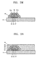
- the protective cap 63 is soft baked at a temperature of about 90° C. for about three minutes. Thereafter, a mask 42 e having a predetermined shape is positioned above the protective cap 63 and ultraviolet rays are radiated as shown in FIG. 3L . By developing the protective cap 63 after radiating the ultraviolet rays, the protective cap 63 is patterned as shown in FIG. 3M . The patterned protective cap 63 is hard baked at a temperature of about 150° C. for about ten minutes, and is argon plasma processed. Thereafter, an inorganic third insulating layer 65 is deposited on the substrate 51 and the protective cap 63 , as shown in FIG. 3N . Here, the argon plasma process is performed to prevent an adhesive force from being weakened when depositing the inorganic third insulating layer 65 on the organic protective cap 63 .
- a contact hole 73 is formed to penetrate the third insulating layer 65 and the protective cap 63 .
- ITO indium tin oxide
- a liquid crystal layer 69 and a second electrode 71 are sequentially formed on the first electrode 67 to construct the pixel unit, and a sealing cap 79 for sealing the pixel unit and the driving unit is coated so that a TFT-LCD 70 is completed.
- FIG. 4 illustrates a sectional view showing a TFT-LCD as an example of a semiconductor device and an electronic device using the same according to a second embodiment of the present invention.
- the structure of a TFT-LCD 100 of FIG. 4 is similar to that of the TFT-LCD 70 of FIG. 2 .
- the semiconductor device according to the second embodiment of the present invention further includes a first protective cap 93 a between a substrate 81 and an active layer 83 in addition to a second protective cap 93 b formed under a third insulating layer 95 .
- Reference numerals 85 , 87 , 89 , 91 a , 91 b , 95 , 97 , 99 , and 101 denote a first insulating layer, a gate electrode, a second insulating layer, a source electrode, a drain electrode, a third insulating layer, a first electrode, a liquid crystal layer, and a second electrode, respectively. Since the semiconductor device and the electronic device using the same according to the second embodiment of the present invention further includes the first protective cap 93 a between the substrate 81 and the active layer 93 along with the second protective cap 93 b , durability against stress due to bending of the substrate 81 may be enhanced.
- FIGS. 5A through 5S illustrate sectional views for showing stages in a manufacturing method of a semiconductor device according to the second embodiment of the present invention.
- an ultraviolet curing resin is coated on a flexible substrate 81 using a spin coating method so that a first protective cap 93 a is formed.
- the first protective cap 93 a is soft baked at a temperature of about 90° C. for about three minutes.
- a mask 72 a is positioned above the first protective cap 93 a , and ultraviolet rays are radiated onto selected portions thereof for about 10 seconds, as shown in FIG. 5B .
- the first protective cap 93 a is dipped into a development solution to remove unexposed portions of the first protective cap 93 a .
- the patterned first protective cap 93 a is hard baked at a temperature of about 150° C. for about ten minutes and argon plasma is processed.
- an amorphous silicon layer 83 a having a thickness of about 50 nm is deposited on the first protective cap 93 a using an RF sputtering process, and photolithography is performed on the amorphous silicon layer 83 a . Accordingly, the patterned amorphous silicon layer 83 a is formed as shown in FIG. 5E .
- reference numeral 72 b denotes a mask and reference numeral 84 denotes a photoresist.
- the amorphous silicon layer 83 a is crystallized by radiating an excimer laser having a wavelength of 308 nm with an overlapping ratio of 95%.
- a second insulating layer 85 is deposited on the active layer 83 , the first protective cap 93 a , and the exposed portions of the substrate 81 using a CVD method, as shown in FIG. 5G .
- a gate electrode 87 is deposited on the second insulating layer 85 using a DC sputtering process.
- a photoresist 84 is coated on the gate electrode 87 , and photolithography is performed on the photoresist 84 . Accordingly, the second insulating layer 85 and the gate electrode 87 are patterned so that a channel region is formed, as shown in FIG. 5H .
- reference numeral 72 c of FIG. 5G denotes a mask.
- a source region S and a drain region D are formed in the active layer 83 by implanting ions to the active layer 83 . Thereafter, the excimer laser is radiated to activate the source and the drain regions S and D.
- a second insulating layer 89 as an ILD layer is deposited on the resultant structure of FIG. 5I , and photolithography is performed using a photoresist 84 and a mask 72 d . Accordingly, portions of the second insulating layer 89 contacting the source and drain regions S and D are removed, as shown in FIG. 5K .
- a source electrode 91 a and a drain electrode 91 b will be formed in the portions at which the second insulating layer 89 is removed in order to electrically connect the source and the drain regions S and D.
- a metal gate electrode layer 91 is deposited on the resultant structure of FIG. 5K and photolithography is performed on the gate electrode layer 91 using a photoresist 84 and a mask 72 e .
- the gate electrode layer 91 is patterned to form a source electrode 91 a and a drain electrode 91 b .
- a second protective cap 93 b is deposited on the resultant structure of FIG. 5M using a spin coating method, and soft baked. Referring to FIG.
- a mask 72 f having a predetermined shape is positioned above the second protective cap 93 b to radiate ultraviolet rays to selected portions of the second protective cap 93 b .
- the second protective cap 93 b is patterned, as shown in FIG. 5P .
- the patterned second protective cap 93 b is hard baked and argon plasma is processed.
- the conditions of the patterning process of the second protective cap 93 b are the same as those of the first protective cap 93 a.
- a third insulating layer 95 is deposited on the substrate 81 and the second protective cap 93 b , as shown in FIG. 5Q .
- a contact hole 103 is formed through the third insulating layer 95 and the second protective cap 93 b to the surface of the drain electrode 91 b.
- a first electrode 97 as a display electrode formed of ITO, is formed on the third insulating layer 95 , and a liquid crystal layer 99 and an ITO second electrode 101 are sequentially formed on the first electrode 97 to form a pixel unit.
- a sealing cap 109 is formed on the pixel unit and a driving unit to complete a TFT-LCD.
- TFTs are examples of semiconductor devices according to the first and the second embodiments of the present invention.
- TFDs thin film diodes
- MIMs metal insulator metals
- the durability of a semiconductor device as disclosed in the first and second embodiments and an electronic device using the same may be improved by forming a protective cap to protect the semiconductor device.
- FIG. 6 illustrates a sectional view showing a TFT-LCD as another example of a semiconductor device and an electronic device using the same according to the first embodiment of the present invention.
- FIG. 7 illustrates a sectional view showing a TFT-LCD as another example of a semiconductor device and an electronic device using the same according to the second embodiment of the present invention.
- first electrodes 127 and 157 as display electrodes are filled in contact holes 133 and 163 that penetrate a protective cap 123 and a second protective cap 153 b , respectively, to connect respective drain electrodes 121 b and 151 b while not including third insulating layers.
- reference numerals 111 and 141 denote flexible substrates
- reference numerals 113 and 143 denote active layers
- reference numerals 115 and 145 denote first insulating layers
- reference numerals 117 and 147 denote gate electrodes
- reference numerals 119 and 149 denote second insulating layers
- reference numerals 121 a and 151 a denote source electrodes
- reference numerals 129 and 159 denote liquid crystal layers
- reference numerals 131 and 161 denote second electrodes
- reference numerals 139 and 169 denote sealing caps.
- the thin film semiconductor device and the electronic device using the same, manufactured as described above, provide the advantage of improved durability against external stress by using the protective cap that seals the thin film semiconductor device.
Abstract
Description
Claims (17)
Priority Applications (1)
| Application Number | Priority Date | Filing Date | Title |
|---|---|---|---|
| US11/702,057 US7767502B2 (en) | 2002-12-31 | 2007-02-05 | Method for manufacturing electronic device using thin film transistor with protective cap over flexible substrate |
Applications Claiming Priority (4)
| Application Number | Priority Date | Filing Date | Title |
|---|---|---|---|
| KR2002-87940 | 2002-12-31 | ||
| KR10-2002-0087940A KR100528326B1 (en) | 2002-12-31 | 2002-12-31 | Thin film semiconductor device with protective cap over flexible substrate and electronic device using the same and manufacturing method thereof |
| US10/748,271 US7176488B2 (en) | 2002-12-31 | 2003-12-31 | Thin film transistor with protective cap over flexible substrate, electronic device using the same, and manufacturing method thereof |
| US11/702,057 US7767502B2 (en) | 2002-12-31 | 2007-02-05 | Method for manufacturing electronic device using thin film transistor with protective cap over flexible substrate |
Related Parent Applications (1)
| Application Number | Title | Priority Date | Filing Date |
|---|---|---|---|
| US10/748,271 Division US7176488B2 (en) | 2002-12-31 | 2003-12-31 | Thin film transistor with protective cap over flexible substrate, electronic device using the same, and manufacturing method thereof |
Publications (2)
| Publication Number | Publication Date |
|---|---|
| US20070172999A1 US20070172999A1 (en) | 2007-07-26 |
| US7767502B2 true US7767502B2 (en) | 2010-08-03 |
Family
ID=32501463
Family Applications (2)
| Application Number | Title | Priority Date | Filing Date |
|---|---|---|---|
| US10/748,271 Expired - Lifetime US7176488B2 (en) | 2002-12-31 | 2003-12-31 | Thin film transistor with protective cap over flexible substrate, electronic device using the same, and manufacturing method thereof |
| US11/702,057 Active 2025-11-18 US7767502B2 (en) | 2002-12-31 | 2007-02-05 | Method for manufacturing electronic device using thin film transistor with protective cap over flexible substrate |
Family Applications Before (1)
| Application Number | Title | Priority Date | Filing Date |
|---|---|---|---|
| US10/748,271 Expired - Lifetime US7176488B2 (en) | 2002-12-31 | 2003-12-31 | Thin film transistor with protective cap over flexible substrate, electronic device using the same, and manufacturing method thereof |
Country Status (5)
| Country | Link |
|---|---|
| US (2) | US7176488B2 (en) |
| EP (1) | EP1435661B1 (en) |
| JP (1) | JP4991092B2 (en) |
| KR (1) | KR100528326B1 (en) |
| CN (1) | CN100462823C (en) |
Cited By (7)
| Publication number | Priority date | Publication date | Assignee | Title |
|---|---|---|---|---|
| US20090262290A1 (en) * | 2007-12-18 | 2009-10-22 | Rockwell Collins, Inc. | Alkali silicate glass for displays |
| US8703365B2 (en) | 2012-03-06 | 2014-04-22 | Apple Inc. | UV mask with anti-reflection coating and UV absorption material |
| US8823003B2 (en) | 2012-08-10 | 2014-09-02 | Apple Inc. | Gate insulator loss free etch-stop oxide thin film transistor |
| US9435915B1 (en) | 2012-09-28 | 2016-09-06 | Rockwell Collins, Inc. | Antiglare treatment for glass |
| US9601557B2 (en) | 2012-11-16 | 2017-03-21 | Apple Inc. | Flexible display |
| US9600112B2 (en) | 2014-10-10 | 2017-03-21 | Apple Inc. | Signal trace patterns for flexible substrates |
| US10411084B2 (en) | 2016-12-26 | 2019-09-10 | Lg Display Co., Ltd. | Flexible display device providing structures to minimize failure generated in bent portion |
Families Citing this family (37)
| Publication number | Priority date | Publication date | Assignee | Title |
|---|---|---|---|---|
| US20050205999A1 (en) * | 2003-08-30 | 2005-09-22 | Visible Tech-Knowledgy, Inc. | Method for pattern metalization of substrates |
| US20050263903A1 (en) * | 2003-08-30 | 2005-12-01 | Visible Tech-Knowledgy, Inc. | Method for pattern metalization of substrates |
| JP2007511786A (en) * | 2003-10-27 | 2007-05-10 | イー インク コーポレイション | Electro-optic display |
| US7098544B2 (en) * | 2004-01-06 | 2006-08-29 | International Business Machines Corporation | Edge seal for integrated circuit chips |
| JP2006041135A (en) * | 2004-07-26 | 2006-02-09 | Sumitomo Bakelite Co Ltd | Electronic device and manufacturing method thereof |
| KR100683766B1 (en) * | 2005-03-30 | 2007-02-15 | 삼성에스디아이 주식회사 | Flat panel display and method for fabricating the same |
| KR20070016772A (en) * | 2005-08-05 | 2007-02-08 | 삼성전자주식회사 | Adhesive tape for flexible display device and method of manufacturing flexible display device using the same0 |
| KR100751453B1 (en) * | 2006-06-14 | 2007-08-23 | 삼성전자주식회사 | Display device and manufacturing method thereof |
| KR101446226B1 (en) * | 2006-11-27 | 2014-10-01 | 엘지디스플레이 주식회사 | Flexible display device and manufacturing method thereof |
| US7629206B2 (en) * | 2007-02-26 | 2009-12-08 | 3M Innovative Properties Company | Patterning self-aligned transistors using back surface illumination |
| US8047442B2 (en) * | 2007-12-03 | 2011-11-01 | Semiconductor Energy Laboratory Co., Ltd. | Semiconductor device |
| TW201001624A (en) * | 2008-01-24 | 2010-01-01 | Soligie Inc | Silicon thin film transistors, systems, and methods of making same |
| US20110068332A1 (en) * | 2008-08-04 | 2011-03-24 | The Trustees Of Princeton University | Hybrid Dielectric Material for Thin Film Transistors |
| KR101928402B1 (en) * | 2009-10-30 | 2018-12-12 | 가부시키가이샤 한도오따이 에네루기 켄큐쇼 | Semiconductor device and method for manufacturing the same |
| US8288857B2 (en) * | 2010-09-17 | 2012-10-16 | Endicott Interconnect Technologies, Inc. | Anti-tamper microchip package based on thermal nanofluids or fluids |
| KR101788317B1 (en) * | 2010-10-28 | 2017-11-15 | 엘지디스플레이 주식회사 | Thin Film Transistor and Method of fabricating Plate Display Device having the same |
| TWI570809B (en) | 2011-01-12 | 2017-02-11 | 半導體能源研究所股份有限公司 | Semiconductor device and manufacturing method thereof |
| US8492874B2 (en) | 2011-02-04 | 2013-07-23 | Qualcomm Incorporated | High density metal-insulator-metal trench capacitor |
| KR101922603B1 (en) * | 2011-03-04 | 2018-11-27 | 가부시키가이샤 한도오따이 에네루기 켄큐쇼 | Light-emitting device, lighting device, substrate, and manufacturing method of substrate |
| KR101942515B1 (en) * | 2012-05-03 | 2019-01-28 | 삼성디스플레이 주식회사 | Organic light emitting display apparatus and method of manufacturing the same |
| US8932945B2 (en) * | 2012-07-09 | 2015-01-13 | Taiwan Semiconductor Manufacturing Company, Ltd. | Wafer alignment system and method |
| JP2014138179A (en) * | 2013-01-18 | 2014-07-28 | Nippon Hoso Kyokai <Nhk> | Thin film transistor array substrate and display device |
| TWI613709B (en) | 2013-02-20 | 2018-02-01 | 財團法人工業技術研究院 | Semiconductor device structure, method for manufacturing the same and pixel structure using the same |
| KR102034253B1 (en) * | 2013-04-12 | 2019-10-21 | 삼성디스플레이 주식회사 | Organic light emitting display apparatus and the manufacturing method thereof |
| KR102089246B1 (en) * | 2013-07-19 | 2020-03-16 | 엘지디스플레이 주식회사 | Flexible Display Device and Method of Fabricating Flexible Display Device |
| CN103545320B (en) * | 2013-11-11 | 2015-11-25 | 京东方科技集团股份有限公司 | Display base plate and the flexible display apparatus containing this display base plate |
| TWI555150B (en) | 2014-05-27 | 2016-10-21 | 財團法人工業技術研究院 | Electronic component and manufacturing method thereof |
| US9391208B2 (en) * | 2014-10-17 | 2016-07-12 | Industrial Technology Research Institute | Electronic device and method of manufacturing the same |
| CN104895885B (en) * | 2015-05-19 | 2017-11-03 | 浙江水晶光电科技股份有限公司 | The curing and device of a kind of group of vertical part |
| US10083989B2 (en) | 2015-12-10 | 2018-09-25 | Industrial Technology Research Institute | Semiconductor device |
| US10429892B1 (en) * | 2016-01-12 | 2019-10-01 | Apple Inc. | Electronic devices with thin display housings |
| CN107134496B (en) * | 2016-02-29 | 2019-05-31 | 昆山工研院新型平板显示技术中心有限公司 | Thin film transistor (TFT) and its manufacturing method, display panel and display device |
| KR102559838B1 (en) * | 2016-04-08 | 2023-07-27 | 삼성디스플레이 주식회사 | Display apparatus |
| CN106129096B (en) * | 2016-08-29 | 2019-08-20 | 武汉华星光电技术有限公司 | A kind of flexible back plate and preparation method thereof, flexible display apparatus |
| CN108122927B (en) * | 2016-11-29 | 2021-01-29 | 昆山工研院新型平板显示技术中心有限公司 | Thin film transistor, manufacturing method thereof, display panel and display device |
| CN109427911B (en) * | 2017-08-31 | 2021-12-14 | 昆山国显光电有限公司 | Flexible thin film transistor and preparation method thereof |
| KR102620972B1 (en) * | 2018-10-23 | 2024-01-05 | 삼성디스플레이 주식회사 | Display apparatus |
Citations (15)
| Publication number | Priority date | Publication date | Assignee | Title |
|---|---|---|---|---|
| JP2000101091A (en) | 1998-09-28 | 2000-04-07 | Sharp Corp | Thin film transistor |
| US20010017372A1 (en) | 2000-02-29 | 2001-08-30 | Semiconductor Energy Laboratory Co., Ltd. | Display device and method for fabricating the same |
| KR20010084247A (en) | 2000-02-24 | 2001-09-06 | 구자홍 | thin film transistor and method for fabricating the same |
| US6329226B1 (en) | 2000-06-01 | 2001-12-11 | Agere Systems Guardian Corp. | Method for fabricating a thin-film transistor |
| US20010050532A1 (en) | 2000-01-31 | 2001-12-13 | Mitsuru Eida | Organic electroluminescence display device and method of manufacturing same |
| US20020036267A1 (en) | 2000-03-28 | 2002-03-28 | Mitsushi Ikeda | Planar X-ray detector |
| US20020057055A1 (en) | 2000-10-26 | 2002-05-16 | Shunpei Yamazaki | Light emitting device and manufacturing method thereof |
| US20020097362A1 (en) | 1996-12-20 | 2002-07-25 | Sharp Kabushiki Kaishi | Liquid crystal display device and method for producing the same |
| US20020155729A1 (en) | 2001-02-21 | 2002-10-24 | Lucent Technologies, Inc. | Semiconductor device encapsulation |
| US20030107688A1 (en) | 2000-12-25 | 2003-06-12 | Machio Yamagishi | Image display |
| KR100390457B1 (en) | 2001-06-01 | 2003-07-07 | 엘지.필립스 엘시디 주식회사 | A structure of thin film transistor and a method for manufacturing the same |
| JP2003255857A (en) | 2002-02-28 | 2003-09-10 | Nippon Hoso Kyokai <Nhk> | Organic el display |
| US6916681B2 (en) | 2001-04-13 | 2005-07-12 | Sony Corporation | Method for manufacturing thin film device and semiconductor device using a third substrate |
| US20050205868A1 (en) | 1998-11-02 | 2005-09-22 | Semiconductor Energy Laboratory Co., Ltd | Semiconductor device and manufacturing method therefor |
| US6992439B2 (en) * | 2001-02-22 | 2006-01-31 | Semiconductor Energy Laboratory Co., Ltd. | Display device with sealing structure for protecting organic light emitting element |
Family Cites Families (4)
| Publication number | Priority date | Publication date | Assignee | Title |
|---|---|---|---|---|
| JPH06125087A (en) * | 1992-10-12 | 1994-05-06 | Ricoh Co Ltd | Semiconductor device |
| JP2001284342A (en) * | 2000-01-25 | 2001-10-12 | Semiconductor Energy Lab Co Ltd | Method of manufacturing optoelectronic device |
| JP2002203682A (en) * | 2000-10-26 | 2002-07-19 | Semiconductor Energy Lab Co Ltd | Light-emitting device and its manufacturing method |
| JP2002182587A (en) * | 2000-12-15 | 2002-06-26 | Sharp Corp | Active matrix substrate and method for manufacturing the same |
-
2002
- 2002-12-31 KR KR10-2002-0087940A patent/KR100528326B1/en active IP Right Grant
-
2003
- 2003-12-24 EP EP03258178A patent/EP1435661B1/en not_active Expired - Lifetime
- 2003-12-31 US US10/748,271 patent/US7176488B2/en not_active Expired - Lifetime
- 2003-12-31 CN CNB2003101249028A patent/CN100462823C/en not_active Expired - Lifetime
-
2004
- 2004-01-05 JP JP2004000067A patent/JP4991092B2/en not_active Expired - Lifetime
-
2007
- 2007-02-05 US US11/702,057 patent/US7767502B2/en active Active
Patent Citations (18)
| Publication number | Priority date | Publication date | Assignee | Title |
|---|---|---|---|---|
| US20020097362A1 (en) | 1996-12-20 | 2002-07-25 | Sharp Kabushiki Kaishi | Liquid crystal display device and method for producing the same |
| JP2000101091A (en) | 1998-09-28 | 2000-04-07 | Sharp Corp | Thin film transistor |
| US20050205868A1 (en) | 1998-11-02 | 2005-09-22 | Semiconductor Energy Laboratory Co., Ltd | Semiconductor device and manufacturing method therefor |
| US6633121B2 (en) | 2000-01-31 | 2003-10-14 | Idemitsu Kosan Co., Ltd. | Organic electroluminescence display device and method of manufacturing same |
| US20010050532A1 (en) | 2000-01-31 | 2001-12-13 | Mitsuru Eida | Organic electroluminescence display device and method of manufacturing same |
| CN1358404A (en) | 2000-01-31 | 2002-07-10 | 出光兴产株式会社 | Organic electroluminescent display device and method of manufacturing the same |
| KR20010084247A (en) | 2000-02-24 | 2001-09-06 | 구자홍 | thin film transistor and method for fabricating the same |
| US20010017372A1 (en) | 2000-02-29 | 2001-08-30 | Semiconductor Energy Laboratory Co., Ltd. | Display device and method for fabricating the same |
| CN1311522A (en) | 2000-02-29 | 2001-09-05 | 株式会社半导体能源研究所 | Displaying device and its mfg. method |
| US20020036267A1 (en) | 2000-03-28 | 2002-03-28 | Mitsushi Ikeda | Planar X-ray detector |
| US6329226B1 (en) | 2000-06-01 | 2001-12-11 | Agere Systems Guardian Corp. | Method for fabricating a thin-film transistor |
| US20020057055A1 (en) | 2000-10-26 | 2002-05-16 | Shunpei Yamazaki | Light emitting device and manufacturing method thereof |
| US20030107688A1 (en) | 2000-12-25 | 2003-06-12 | Machio Yamagishi | Image display |
| US20020155729A1 (en) | 2001-02-21 | 2002-10-24 | Lucent Technologies, Inc. | Semiconductor device encapsulation |
| US6992439B2 (en) * | 2001-02-22 | 2006-01-31 | Semiconductor Energy Laboratory Co., Ltd. | Display device with sealing structure for protecting organic light emitting element |
| US6916681B2 (en) | 2001-04-13 | 2005-07-12 | Sony Corporation | Method for manufacturing thin film device and semiconductor device using a third substrate |
| KR100390457B1 (en) | 2001-06-01 | 2003-07-07 | 엘지.필립스 엘시디 주식회사 | A structure of thin film transistor and a method for manufacturing the same |
| JP2003255857A (en) | 2002-02-28 | 2003-09-10 | Nippon Hoso Kyokai <Nhk> | Organic el display |
Non-Patent Citations (4)
| Title |
|---|
| Hur, Ji Ho, et al., "Late-News Paper: A 2 inch A-Si:H TFT-LCD on Plastic", 2002 SID International Symposium Digest of Technical Papers, Boston, MA (US), May 21-23, 2002 [SID 02 Digest] vol. 33, No. 2, pp. 802-805 (May 2002). |
| Patent Abstracts of Japan, vol. 2003, No. 12, (Dec. 5, 2003) & JP 2003 255857 Nippon Hoso Kyokai . |
| Patent Abstracts of Japan, vol. 2003, No. 12, (Dec. 5, 2003) & JP 2003 255857 Nippon Hoso Kyokai <NHK>. |
| Suo, Z., et al., "Mechanics of rollable and foldable fillm-on-foil electronics" Applied Physics Letters, vol. 74, No. 8, pp. 1177-1179, (Feb. 22, 1999). |
Cited By (8)
| Publication number | Priority date | Publication date | Assignee | Title |
|---|---|---|---|---|
| US20090262290A1 (en) * | 2007-12-18 | 2009-10-22 | Rockwell Collins, Inc. | Alkali silicate glass for displays |
| US8703365B2 (en) | 2012-03-06 | 2014-04-22 | Apple Inc. | UV mask with anti-reflection coating and UV absorption material |
| US8823003B2 (en) | 2012-08-10 | 2014-09-02 | Apple Inc. | Gate insulator loss free etch-stop oxide thin film transistor |
| US8987049B2 (en) | 2012-08-10 | 2015-03-24 | Apple Inc. | Gate insulator loss free etch-stop oxide thin film transistor |
| US9435915B1 (en) | 2012-09-28 | 2016-09-06 | Rockwell Collins, Inc. | Antiglare treatment for glass |
| US9601557B2 (en) | 2012-11-16 | 2017-03-21 | Apple Inc. | Flexible display |
| US9600112B2 (en) | 2014-10-10 | 2017-03-21 | Apple Inc. | Signal trace patterns for flexible substrates |
| US10411084B2 (en) | 2016-12-26 | 2019-09-10 | Lg Display Co., Ltd. | Flexible display device providing structures to minimize failure generated in bent portion |
Also Published As
| Publication number | Publication date |
|---|---|
| EP1435661A3 (en) | 2006-01-18 |
| EP1435661A2 (en) | 2004-07-07 |
| KR20040061656A (en) | 2004-07-07 |
| US20040149987A1 (en) | 2004-08-05 |
| JP2004214683A (en) | 2004-07-29 |
| CN1527115A (en) | 2004-09-08 |
| US20070172999A1 (en) | 2007-07-26 |
| KR100528326B1 (en) | 2005-11-15 |
| CN100462823C (en) | 2009-02-18 |
| JP4991092B2 (en) | 2012-08-01 |
| EP1435661B1 (en) | 2012-05-02 |
| US7176488B2 (en) | 2007-02-13 |
Similar Documents
| Publication | Publication Date | Title |
|---|---|---|
| US7767502B2 (en) | Method for manufacturing electronic device using thin film transistor with protective cap over flexible substrate | |
| US8081266B2 (en) | Thin film transistor device, liquid crystal display device using the same, and method of fabricating the same | |
| US8324033B2 (en) | TFT array substrate and manufacturing method thereof | |
| US7511300B2 (en) | Array substrate, display device having the same and method of manufacturing the same | |
| US8551825B2 (en) | Method for fabricating a thin film transistor with an organic passivation layer | |
| US8053295B2 (en) | Liquid crystal display device and method of fabricating the same | |
| GB2418065A (en) | Organic thin film transistor formed by rear exposure method | |
| KR20020092039A (en) | Method for Processing Surface of Organic Isolation Film and Method of Fabricating Thin Film Transistor Substate using the same | |
| US7157315B2 (en) | Active matrix substrate and method of fabricating the same | |
| US7605889B2 (en) | Pixel structure and fabrication method thereof | |
| CN213304143U (en) | Display panel | |
| KR20150063841A (en) | Method of fabricating flexible organic light emitting diode display device | |
| US10714504B2 (en) | Low temperature poly-silicon thin film transistor array substrate and method of producing the same | |
| CN107342298A (en) | Display device, array base palte and its manufacture method | |
| TWI330502B (en) | Method of manufacturing an amoled | |
| KR100936889B1 (en) | A array substrate and the fabrication method for LCD | |
| KR20020002655A (en) | Method of manufacturing tft-lcd | |
| KR100776753B1 (en) | Method of manufacturing polycrystalline thin film transistor for liquid crystal device | |
| KR100878230B1 (en) | a method for manufacturing a thin film transistor substrate | |
| KR20070120766A (en) | Organic thin film transistor liquid crystal display device and the method for fabricating thereof | |
| KR20020095543A (en) | a method for manufacturing a thin film transistor substrate |
Legal Events
| Date | Code | Title | Description |
|---|---|---|---|
| STCF | Information on status: patent grant |
Free format text: PATENTED CASE |
|
| FEPP | Fee payment procedure |
Free format text: PAYOR NUMBER ASSIGNED (ORIGINAL EVENT CODE: ASPN); ENTITY STATUS OF PATENT OWNER: LARGE ENTITY |
|
| FEPP | Fee payment procedure |
Free format text: PAYER NUMBER DE-ASSIGNED (ORIGINAL EVENT CODE: RMPN); ENTITY STATUS OF PATENT OWNER: LARGE ENTITY Free format text: PAYOR NUMBER ASSIGNED (ORIGINAL EVENT CODE: ASPN); ENTITY STATUS OF PATENT OWNER: LARGE ENTITY |
|
| FPAY | Fee payment |
Year of fee payment: 4 |
|
| MAFP | Maintenance fee payment |
Free format text: PAYMENT OF MAINTENANCE FEE, 8TH YEAR, LARGE ENTITY (ORIGINAL EVENT CODE: M1552) Year of fee payment: 8 |
|
| MAFP | Maintenance fee payment |
Free format text: PAYMENT OF MAINTENANCE FEE, 12TH YEAR, LARGE ENTITY (ORIGINAL EVENT CODE: M1553); ENTITY STATUS OF PATENT OWNER: LARGE ENTITY Year of fee payment: 12 |