US7772082B2 - Capacitor of semiconductor device and method of fabricating the same - Google Patents
Capacitor of semiconductor device and method of fabricating the same Download PDFInfo
- Publication number
- US7772082B2 US7772082B2 US11/987,989 US98798907A US7772082B2 US 7772082 B2 US7772082 B2 US 7772082B2 US 98798907 A US98798907 A US 98798907A US 7772082 B2 US7772082 B2 US 7772082B2
- Authority
- US
- United States
- Prior art keywords
- storage node
- film
- insulating film
- buffer insulating
- pattern
- Prior art date
- Legal status (The legal status is an assumption and is not a legal conclusion. Google has not performed a legal analysis and makes no representation as to the accuracy of the status listed.)
- Expired - Fee Related, expires
Links
Images


Classifications
-
- H—ELECTRICITY
- H10—SEMICONDUCTOR DEVICES; ELECTRIC SOLID-STATE DEVICES NOT OTHERWISE PROVIDED FOR
- H10B—ELECTRONIC MEMORY DEVICES
- H10B12/00—Dynamic random access memory [DRAM] devices
-
- H—ELECTRICITY
- H01—ELECTRIC ELEMENTS
- H01L—SEMICONDUCTOR DEVICES NOT COVERED BY CLASS H10
- H01L28/00—Passive two-terminal components without a potential-jump or surface barrier for integrated circuits; Details thereof; Multistep manufacturing processes therefor
- H01L28/40—Capacitors
- H01L28/60—Electrodes
- H01L28/82—Electrodes with an enlarged surface, e.g. formed by texturisation
- H01L28/90—Electrodes with an enlarged surface, e.g. formed by texturisation having vertical extensions
- H01L28/91—Electrodes with an enlarged surface, e.g. formed by texturisation having vertical extensions made by depositing layers, e.g. by depositing alternating conductive and insulating layers
Definitions
- the invention generally relates to a semiconductor device. More particularly, the invention relates to a method of fabricating a semiconductor device including a capacitor.
- the memory capability is increased.
- the high integration of the device increases a chip area but decreases a cell area.
- the reduction of the cell area decreases an area of a cell capacitor.
- the read-out capability of the cell is reduced, the durability is degraded by soft errors of alpha particles, and a sensing margin of a sense amplifier is decreased. Therefore, a method for securing a sufficient capacitance in a limited cell region is required.
- the capacitance refers to a capacity of charges stored in a capacitor. As a capacitance becomes larger, more information can be stored.
- the capacitance is represented by Equation 1.
- ⁇ is a dielectric constant determined by kinds of dielectric films disposed between two electrodes, d is a distance between the two electrodes, and A is an effective surface of the two electrodes. Referring to Equation 1, as ⁇ is larger, d is shorter between the two electrodes and A of the two electrodes is increased, the capacitance of the capacitor can be increased.
- the electrode structure of the capacitor is changed to have a three-dimensional type such as a concave structure and a cylinder structure, thereby increasing the effective area of the electrodes.
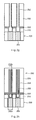
- FIGS. 1 a to 1 e are cross-sectional views illustrating a conventional method of fabricating a semiconductor device.
- a buffer oxide film 110 , an etch stop film 115 , an interlayer insulating film 120 and a hard mask layer 130 are sequentially formed over a semiconductor substrate 100 including a storage node contact plug 105 .
- a silicon oxynitride (SiON) film and a photoresist pattern (not shown) defining a storage node region are formed over hard mask layer 130 .
- Buffer oxide film 110 plays a role of compensating non-uniformity of semiconductor substrate 100 .
- Etch stop film 115 includes a nitride film having the etching selectivity over interlayer insulating film 120 to stop an etching process.
- a silicon oxide nitride film (not shown) and hard mask layer 130 are sequentially etched using photoresist pattern as a mask.
- the oxynitride film and the photoresist pattern are removed.
- Interlayer insulating film 120 is etched using hard mask layer 130 as an etching mask to form a storage node region 117 that exposes etch stop film 115 .
- Exposed etch stop film 115 at the bottom of storage node region 117 and underlying buffer oxide film 110 are sequentially etched to expose storage node contact plug 105 .
- a first conductive layer 150 is formed over semiconductor substrate 100 including storage node region 117 .
- first conductive layer 150 is planarized until interlayer insulating film 120 is exposed.
- a full dip-out process is performed to remove interlayer insulating film 120 , thereby forming a cylinder-type lower storage node 152 .
- a space margin is insufficient to cause a leaning phenomenon of lower storage node 152 .
- a thickness of the interlayer insulating film is increased.
- an etch depth is deepened when the interlayer insulating film is etched so that it is difficult to secure a lower line-width of the storage node region.
- the buffer oxide film and the etch stop film prevent a leaning phenomenon of the cylinder-type lower storage node, a sufficient depth is not secured to prevent the leaning of the capacitor.
- Embodiments of the invention are directed to a semiconductor device.
- the semiconductor device includes a buffer insulating pattern to define a region wider than a storage node region with a storage node mask.
- the semiconductor device includes a capacitor that secures a line-width of a lower part of a lower storage node to prevent a leaning phenomenon of the capacitor, thereby improving reliability of the device. Also, an aspect ratio of the capacitor is increased to secure capacitance of the capacitor, thereby improving characteristics of the device.
- a method of fabricating a semiconductor device includes forming a buffer insulating film over a semiconductor substrate including a conductive pattern.
- the buffer insulating film is etched using a storage node mask to form a buffer insulating pattern exposing the conductive pattern.
- the buffer insulating pattern defines a region wider than a storage node region.
- An etch stop film is formed over the conductive pattern and the buffer insulating pattern.
- An interlayer insulating film is formed over the etch stop film.
- the interlayer insulating film is etched using the storage node mask to expose the etch stop film.
- the exposed etch stop film is removed to expose the conductive pattern on the bottom and both sidewalls of the buffer insulating pattern, thereby forming a storage node region.
- a lining lower storage node is formed over the storage node region.
- FIGS. 1 a to 1 e are cross-sectional views illustrating a conventional method of fabricating a semiconductor device.
- FIGS. 2 a to 2 h are cross-sectional views illustrating a method of fabricating a semiconductor device according to an embodiment of the invention.
- the invention relates to a method of fabricating a semiconductor device.
- a buffer insulating pattern defining a region wider than a storage node region is formed using a storage node mask so as to obtain a capacitor.
- FIGS. 2 a to 2 h are cross-sectional views illustrating a method of fabricating a semiconductor device according to an embodiment of the invention.
- a buffer insulating film 206 is formed over a semiconductor substrate 200 including a storage node contact plug 205 .
- Buffer insulating film 206 includes an oxide film.
- Buffer insulating film 206 has a thickness in a range of about 1,000 ⁇ to about 2,000 ⁇ .
- a photoresist film (not shown) is formed over buffer oxide film 206 .
- the photoresist film is exposed and developed using a storage node mask to form a first photoresist pattern 208 .
- First photoresist pattern 207 is over-exposed to define a region wider than a storage node region defined in the exposure mask.
- Buffer insulating film 206 is etched using first photoresist pattern 208 as a mask to form a buffer insulating pattern 210 that exposes storage node contact plug 205 .
- First photoresist pattern 208 is removed.
- an etch stop film 220 is formed over storage node contact plug 205 and buffer insulating film 210 .
- Etch stop film 220 has the etching selectivity over a subsequent interlayer insulating film.
- etch stop film 220 includes a nitride film.
- Interlayer insulating film 230 and hard mask layer 240 are formed over etch stop film 220 .
- Interlayer insulating film 230 is selected from the group consisting of a phosphorous-silicate-glass (“PSG”) oxide film, a plasma enhanced tetra-ethyl-ortho-silicate glass (“PE-TEOS”) oxide film and a combination thereof.
- a thickness of interlayer insulating film 230 is adjusted depending on a height of the lower storage node.
- Hard mask layer 240 includes a carbon layer.
- a silicon oxynitride (SiON) film 244 is formed over hard mask layer 240 .
- a photoresist film is formed over silicon oxynitride film 244 .
- the photoresist film is exposed and developed using the storage node mask to form a second photoresist pattern 246 that defines a storage node region.
- the storage node mask is the same as the mask used when buffer insulating pattern 210 is formed.
- Silicon oxynitride film 244 and hard mask layer 240 are etched using second photoresist pattern 246 as an etching mask to form a hard mask pattern 242 .
- Interlayer insulating film 230 is etched using hard mask pattern 242 as a mask to expose etch stop film 220 . Second photoresist pattern 246 is removed.
- exposed etch stop film 220 is removed to form a storage node region 248 that exposes the storage node contact plug 205 .
- a selective etching method is performed with an etching selectivity difference between interlayer insulating film 230 and etch stop film 220 to remove etch stop film 220 .
- etch stop film 220 formed over a sidewall of buffer insulating film 210 is removed.
- a line-width 248 a of the lower part of storage node region 248 is wider than a line-width 248 b of an upper part of storage node region 248 .
- a subsequent lower storage node is substantially supported from the lower part of storage node region 248 .
- a conductive layer 250 is formed over storage node contact plug 205 including storage node region 248 , buffer insulating pattern 210 , interlayer insulating film 230 , hard mask pattern 242 and silicon oxynitride film 244 .
- Conductive layer 250 is selected from the group consisting of a titanium layer, a titanium nitride film and a combination thereof.
- a planarization process is performed on conductive layer 250 to expose interlayer insulating film 230 , thereby isolating lower storage node 252 .
- a full dip-out process is performed to remove interlayer insulating film 230 , thereby exposing cylinder-type lower storage node 252 .
- a bottom of lower storage node 252 is supported by buffer insulating pattern 210 .
- Line-width 252 a of a lower part of lower storage node 252 is wider than line-width 252 b of an upper part of lower storage node 252 , which prevents a leaning phenomenon of lower storage node 252 during the dip-out process.
- a dielectric layer 254 and a plate electrode 256 are formed over lower storage node 252 to obtain a capacitor 260 .
- a sufficient lower line-width of a lower storage node region is secured to obtain a solid lower storage node, thereby preventing a leaning phenomenon of the lower storage node.
Abstract
A method of fabricating a semiconductor device includes forming a buffer insulating film over a semiconductor substrate including a conductive pattern. The buffer insulating film is etched using a storage node mask to form a buffer insulating pattern exposing the conductive pattern. The buffer insulating pattern defines a region wider than a storage node region. An etch stop film is formed over the conductive pattern and the buffer insulating pattern. An interlayer insulating film is formed over the etch stop film. The interlayer insulating film is etched using the storage node mask to expose the etch stop film. The exposed etch stop film is etched to form the storage node region exposing conductive pattern. A lower storage node is formed over the storage node region.
Description
This application is based upon and claims the benefit of priority to Korean Patent Application No. 10-2007-0038907, filed on Apr. 20, 2007, the entire contents of which are incorporated herein by reference.
The invention generally relates to a semiconductor device. More particularly, the invention relates to a method of fabricating a semiconductor device including a capacitor.
As a semiconductor device becomes smaller and more highly integrated, the memory capability is increased. However, the high integration of the device increases a chip area but decreases a cell area. The reduction of the cell area decreases an area of a cell capacitor. As a result, the read-out capability of the cell is reduced, the durability is degraded by soft errors of alpha particles, and a sensing margin of a sense amplifier is decreased. Therefore, a method for securing a sufficient capacitance in a limited cell region is required.
The capacitance refers to a capacity of charges stored in a capacitor. As a capacitance becomes larger, more information can be stored. The capacitance is represented by Equation 1.
∈ is a dielectric constant determined by kinds of dielectric films disposed between two electrodes, d is a distance between the two electrodes, and A is an effective surface of the two electrodes. Referring to Equation 1, as ∈ is larger, d is shorter between the two electrodes and A of the two electrodes is increased, the capacitance of the capacitor can be increased. The electrode structure of the capacitor is changed to have a three-dimensional type such as a concave structure and a cylinder structure, thereby increasing the effective area of the electrodes.
Referring to FIGS. 1 b to 1 d, a silicon oxide nitride film (not shown) and hard mask layer 130 are sequentially etched using photoresist pattern as a mask. The oxynitride film and the photoresist pattern are removed. Interlayer insulating film 120 is etched using hard mask layer 130 as an etching mask to form a storage node region 117 that exposes etch stop film 115. Exposed etch stop film 115 at the bottom of storage node region 117 and underlying buffer oxide film 110 are sequentially etched to expose storage node contact plug 105. A first conductive layer 150 is formed over semiconductor substrate 100 including storage node region 117.
Referring to FIG. 1 e, first conductive layer 150 is planarized until interlayer insulating film 120 is exposed. A full dip-out process is performed to remove interlayer insulating film 120, thereby forming a cylinder-type lower storage node 152. In the dip-out process, a space margin is insufficient to cause a leaning phenomenon of lower storage node 152.
However, as a height of a capacitor electrode is increased, a thickness of the interlayer insulating film is increased. As a result, an etch depth is deepened when the interlayer insulating film is etched so that it is difficult to secure a lower line-width of the storage node region. Although the buffer oxide film and the etch stop film prevent a leaning phenomenon of the cylinder-type lower storage node, a sufficient depth is not secured to prevent the leaning of the capacitor.
Embodiments of the invention are directed to a semiconductor device. According to one embodiment of the invention, the semiconductor device includes a buffer insulating pattern to define a region wider than a storage node region with a storage node mask. The semiconductor device includes a capacitor that secures a line-width of a lower part of a lower storage node to prevent a leaning phenomenon of the capacitor, thereby improving reliability of the device. Also, an aspect ratio of the capacitor is increased to secure capacitance of the capacitor, thereby improving characteristics of the device.
According to another embodiment of the invention, a method of fabricating a semiconductor device includes forming a buffer insulating film over a semiconductor substrate including a conductive pattern. The buffer insulating film is etched using a storage node mask to form a buffer insulating pattern exposing the conductive pattern. The buffer insulating pattern defines a region wider than a storage node region. An etch stop film is formed over the conductive pattern and the buffer insulating pattern. An interlayer insulating film is formed over the etch stop film. The interlayer insulating film is etched using the storage node mask to expose the etch stop film. The exposed etch stop film is removed to expose the conductive pattern on the bottom and both sidewalls of the buffer insulating pattern, thereby forming a storage node region. A lining lower storage node is formed over the storage node region.
The invention relates to a method of fabricating a semiconductor device. In one embodiment of the invention, a buffer insulating pattern defining a region wider than a storage node region is formed using a storage node mask so as to obtain a capacitor.
A photoresist film (not shown) is formed over buffer oxide film 206. The photoresist film is exposed and developed using a storage node mask to form a first photoresist pattern 208. First photoresist pattern 207 is over-exposed to define a region wider than a storage node region defined in the exposure mask. Buffer insulating film 206 is etched using first photoresist pattern 208 as a mask to form a buffer insulating pattern 210 that exposes storage node contact plug 205. First photoresist pattern 208 is removed.
Referring to FIG. 2 c, an etch stop film 220 is formed over storage node contact plug 205 and buffer insulating film 210. Etch stop film 220 has the etching selectivity over a subsequent interlayer insulating film. For example, etch stop film 220 includes a nitride film.
Referring to FIG. 2 d, a photoresist film is formed over silicon oxynitride film 244. The photoresist film is exposed and developed using the storage node mask to form a second photoresist pattern 246 that defines a storage node region. The storage node mask is the same as the mask used when buffer insulating pattern 210 is formed. Silicon oxynitride film 244 and hard mask layer 240 are etched using second photoresist pattern 246 as an etching mask to form a hard mask pattern 242. Interlayer insulating film 230 is etched using hard mask pattern 242 as a mask to expose etch stop film 220. Second photoresist pattern 246 is removed.
Referring to FIGS. 2 e to 2 g, exposed etch stop film 220 is removed to form a storage node region 248 that exposes the storage node contact plug 205. A selective etching method is performed with an etching selectivity difference between interlayer insulating film 230 and etch stop film 220 to remove etch stop film 220. In a lower part of the storage node region 248, etch stop film 220 formed over a sidewall of buffer insulating film 210 is removed. A line-width 248 a of the lower part of storage node region 248 is wider than a line-width 248 b of an upper part of storage node region 248. As a result, a subsequent lower storage node is substantially supported from the lower part of storage node region 248.
A conductive layer 250 is formed over storage node contact plug 205 including storage node region 248, buffer insulating pattern 210, interlayer insulating film 230, hard mask pattern 242 and silicon oxynitride film 244. Conductive layer 250 is selected from the group consisting of a titanium layer, a titanium nitride film and a combination thereof. A planarization process is performed on conductive layer 250 to expose interlayer insulating film 230, thereby isolating lower storage node 252.
Referring to FIG. 2 h, a full dip-out process is performed to remove interlayer insulating film 230, thereby exposing cylinder-type lower storage node 252. A bottom of lower storage node 252 is supported by buffer insulating pattern 210. Line-width 252 a of a lower part of lower storage node 252 is wider than line-width 252 b of an upper part of lower storage node 252, which prevents a leaning phenomenon of lower storage node 252 during the dip-out process. A dielectric layer 254 and a plate electrode 256 are formed over lower storage node 252 to obtain a capacitor 260.
As described above, according to an embodiment of the invention, a sufficient lower line-width of a lower storage node region is secured to obtain a solid lower storage node, thereby preventing a leaning phenomenon of the lower storage node.
Although a number of illustrative embodiments consistent with the invention have been described, it should be understood that numerous other modifications and embodiments can be devised by those skilled in the art that will fall within the spirit and scope of the principles of this disclosure. More particularly, a number of variations and modifications are possible in the component parts and/or arrangements of the subject combination arrangement within the scope of the disclosure, the drawings and the appended claims. In addition to variations and modifications in the component parts and/or arrangements, alternative uses will also be apparent to those skilled in the art.
Claims (8)
1. A method of fabricating a capacitor of a semiconductor device, the method comprising:
forming a buffer insulating film over a semiconductor substrate including conductive patterns;
etching the buffer insulating film using a storage node mask to form a buffer insulating pattern exposing one of the conductive patterns, the buffer insulating pattern defining a first storage node region wider than a second storage node region;
forming an etch stop film over the conductive patterns and the buffer insulating pattern;
forming an interlayer insulating film over the etch stop film;
etching the interlayer insulating film using the storage node mask to expose the etch stop film thereby forming the second storage node region;
removing the exposed etch stop film to expose the conductive patterns on the bottom and both sidewalls of the buffer insulating pattern, thereby forming the first storage node region; and
forming a lining lower storage node over the first and second storage node regions.
2. The method of claim 1 , wherein the process of forming the buffer insulating pattern comprises:
forming a photoresist film over the buffer insulating film;
exposing and developing the photoresist film using the storage node mask to form a photoresist pattern;
etching the buffer insulating film using the photoresist pattern to form the buffer insulating pattern; and
removing the photoresist pattern.
3. The method of claim 2 , wherein the exposing process is performed using an over-exposing method to form the photoresist pattern defining a wider width than that of the second storage node region.
4. The method of claim 1 , wherein the interlayer insulating film is selected from the group consisting of a phosphorous-silicate-glass (PSG) oxide film, a plasma enhanced tetra-ethyl-ortho-silicate glass (PE-TEOS) oxide film, and a combination thereof.
5. The method of claim 1 , further comprising forming a hard mask carbon layer and a silicon oxynitride film over the interlayer insulating film.
6. The method of claim 1 , wherein the buffer insulating film is formed to have a thickness in a range of about 1,000 to 2,000 Å.
7. The method of claim 1 , wherein conductive patterns are storage node contact plugs.
8. The method of claim 1 , wherein a line-width of the first storage node region is wider than a line-width of the second storage node region.
Priority Applications (1)
| Application Number | Priority Date | Filing Date | Title |
|---|---|---|---|
| US12/821,093 US20100258906A1 (en) | 2007-04-20 | 2010-06-22 | Capacitor of semiconductor device and method of fabricating the same |
Applications Claiming Priority (2)
| Application Number | Priority Date | Filing Date | Title |
|---|---|---|---|
| KR1020070038907A KR100924207B1 (en) | 2007-04-20 | 2007-04-20 | Method for manufacturing semiconductor device |
| KR10-2007-0038907 | 2007-04-20 |
Related Child Applications (1)
| Application Number | Title | Priority Date | Filing Date |
|---|---|---|---|
| US12/821,093 Division US20100258906A1 (en) | 2007-04-20 | 2010-06-22 | Capacitor of semiconductor device and method of fabricating the same |
Publications (2)
| Publication Number | Publication Date |
|---|---|
| US20080261373A1 US20080261373A1 (en) | 2008-10-23 |
| US7772082B2 true US7772082B2 (en) | 2010-08-10 |
Family
ID=39872627
Family Applications (2)
| Application Number | Title | Priority Date | Filing Date |
|---|---|---|---|
| US11/987,989 Expired - Fee Related US7772082B2 (en) | 2007-04-20 | 2007-12-06 | Capacitor of semiconductor device and method of fabricating the same |
| US12/821,093 Abandoned US20100258906A1 (en) | 2007-04-20 | 2010-06-22 | Capacitor of semiconductor device and method of fabricating the same |
Family Applications After (1)
| Application Number | Title | Priority Date | Filing Date |
|---|---|---|---|
| US12/821,093 Abandoned US20100258906A1 (en) | 2007-04-20 | 2010-06-22 | Capacitor of semiconductor device and method of fabricating the same |
Country Status (2)
| Country | Link |
|---|---|
| US (2) | US7772082B2 (en) |
| KR (1) | KR100924207B1 (en) |
Citations (7)
| Publication number | Priority date | Publication date | Assignee | Title |
|---|---|---|---|---|
| US6573030B1 (en) * | 2000-02-17 | 2003-06-03 | Applied Materials, Inc. | Method for depositing an amorphous carbon layer |
| US20040048475A1 (en) | 2002-09-07 | 2004-03-11 | Samsung Electronics Co., Ltd. | Method for forming a storage node of a capacitor |
| KR20050090831A (en) | 2004-03-10 | 2005-09-14 | 삼성전자주식회사 | Semiconductor memory device and fabrication method thereof |
| KR20050117879A (en) | 2004-06-11 | 2005-12-15 | 삼성전자주식회사 | Method of fabricating cylindrical capacitor of semiconductor device |
| KR20060030820A (en) | 2004-10-06 | 2006-04-11 | 삼성전자주식회사 | Fabrication method of a semiconductor device having a storage node electrode and semiconductor device fabricated thereby |
| KR20060071548A (en) * | 2004-12-22 | 2006-06-27 | 한성석 | An apparatus for supplying oil |
| US7262453B2 (en) * | 2004-02-04 | 2007-08-28 | Samsung Electronics Co., Ltd. | Multiple stacked capacitors formed within an opening with thick capacitor dielectric |
Family Cites Families (3)
| Publication number | Priority date | Publication date | Assignee | Title |
|---|---|---|---|---|
| US6452858B1 (en) * | 1999-11-05 | 2002-09-17 | Hitachi, Ltd. | Semiconductor device |
| KR100388682B1 (en) * | 2001-03-03 | 2003-06-25 | 삼성전자주식회사 | Storage electric terminal layer and method for forming thereof |
| US7067385B2 (en) * | 2003-09-04 | 2006-06-27 | Micron Technology, Inc. | Support for vertically oriented capacitors during the formation of a semiconductor device |
-
2007
- 2007-04-20 KR KR1020070038907A patent/KR100924207B1/en not_active IP Right Cessation
- 2007-12-06 US US11/987,989 patent/US7772082B2/en not_active Expired - Fee Related
-
2010
- 2010-06-22 US US12/821,093 patent/US20100258906A1/en not_active Abandoned
Patent Citations (7)
| Publication number | Priority date | Publication date | Assignee | Title |
|---|---|---|---|---|
| US6573030B1 (en) * | 2000-02-17 | 2003-06-03 | Applied Materials, Inc. | Method for depositing an amorphous carbon layer |
| US20040048475A1 (en) | 2002-09-07 | 2004-03-11 | Samsung Electronics Co., Ltd. | Method for forming a storage node of a capacitor |
| US7262453B2 (en) * | 2004-02-04 | 2007-08-28 | Samsung Electronics Co., Ltd. | Multiple stacked capacitors formed within an opening with thick capacitor dielectric |
| KR20050090831A (en) | 2004-03-10 | 2005-09-14 | 삼성전자주식회사 | Semiconductor memory device and fabrication method thereof |
| KR20050117879A (en) | 2004-06-11 | 2005-12-15 | 삼성전자주식회사 | Method of fabricating cylindrical capacitor of semiconductor device |
| KR20060030820A (en) | 2004-10-06 | 2006-04-11 | 삼성전자주식회사 | Fabrication method of a semiconductor device having a storage node electrode and semiconductor device fabricated thereby |
| KR20060071548A (en) * | 2004-12-22 | 2006-06-27 | 한성석 | An apparatus for supplying oil |
Non-Patent Citations (1)
| Title |
|---|
| Notice of Allowance issued from Korean Intellectual Property Office on Sep. 30, 2009 with an English Translation. |
Also Published As
| Publication number | Publication date |
|---|---|
| KR20080094450A (en) | 2008-10-23 |
| KR100924207B1 (en) | 2009-10-29 |
| US20100258906A1 (en) | 2010-10-14 |
| US20080261373A1 (en) | 2008-10-23 |
Similar Documents
| Publication | Publication Date | Title |
|---|---|---|
| KR102076060B1 (en) | Semiconductor device including capacitors and method for manufacturing the same | |
| US5677222A (en) | Method for forming a DRAM capacitor | |
| US20110165756A1 (en) | Method for manufacturing semiconductor device | |
| US20210013211A1 (en) | Dram semiconductor device having reduced parasitic capacitance between capacitor contacts and bit line structures and method for manufacturing the same | |
| US5902126A (en) | Methods for forming integrated circuit capacitor electrodes including surrounding insulating sidewalls and spacers | |
| JP2006157002A (en) | Manufacturing method of capacitor, and manufacturing method of semiconductor device | |
| US6156608A (en) | Method of manufacturing cylindrical shaped capacitor | |
| US7713832B2 (en) | Semiconductor device and method of fabricating the same | |
| US6709915B2 (en) | Methods of fabricating integrated circuit memory devices | |
| US5913129A (en) | Method of fabricating a capacitor structure for a dynamic random access memory | |
| US20080164566A1 (en) | Method for forming a buried digit line with self aligning spacing layer and contact plugs during the formation of a semiconductor device, semiconductor devices, and systems including same | |
| US7585780B2 (en) | Method for manufacturing semiconductor device | |
| US6413832B1 (en) | Method for forming inner-cylindrical capacitor without top electrode mask | |
| KR20080087304A (en) | Method for fabricating capacitor of semiconductor device | |
| US8129251B2 (en) | Metal-insulator-metal-structured capacitor formed with polysilicon | |
| US20020111006A1 (en) | Method for forming landing pad | |
| US20060148168A1 (en) | Process for fabricating dynamic random access memory | |
| US7772082B2 (en) | Capacitor of semiconductor device and method of fabricating the same | |
| US8105913B2 (en) | Method of fabricating a capacitor of a semiconductor device | |
| KR100476399B1 (en) | Method for making capacitor in semiconductor device | |
| KR100772703B1 (en) | Method of forming capacitor of memory device | |
| US6107132A (en) | Method of manufacturing a DRAM capacitor | |
| US7736971B2 (en) | Semiconductor device and method of fabricating the same | |
| KR20060107130A (en) | Semiconductor device having a storage node electrode and fabrication method thereof | |
| KR100762869B1 (en) | A method for fabricating capacitor |
Legal Events
| Date | Code | Title | Description |
|---|---|---|---|
| AS | Assignment |
Owner name: HYNIX SEMICONDUCTOR INC., KOREA, REPUBLIC OF Free format text: ASSIGNMENT OF ASSIGNORS INTEREST;ASSIGNOR:CHOI, JOONG II;REEL/FRAME:020247/0927 Effective date: 20071126 |
|
| FEPP | Fee payment procedure |
Free format text: PAYOR NUMBER ASSIGNED (ORIGINAL EVENT CODE: ASPN); ENTITY STATUS OF PATENT OWNER: LARGE ENTITY |
|
| REMI | Maintenance fee reminder mailed | ||
| LAPS | Lapse for failure to pay maintenance fees | ||
| STCH | Information on status: patent discontinuation |
Free format text: PATENT EXPIRED DUE TO NONPAYMENT OF MAINTENANCE FEES UNDER 37 CFR 1.362 |
|
| FP | Lapsed due to failure to pay maintenance fee |
Effective date: 20140810 |