US7778359B2 - Method and device for clock synchronisation with a vestigial-sideband-modulated transmitted signal - Google Patents
Method and device for clock synchronisation with a vestigial-sideband-modulated transmitted signal Download PDFInfo
- Publication number
- US7778359B2 US7778359B2 US11/302,320 US30232005A US7778359B2 US 7778359 B2 US7778359 B2 US 7778359B2 US 30232005 A US30232005 A US 30232005A US 7778359 B2 US7778359 B2 US 7778359B2
- Authority
- US
- United States
- Prior art keywords
- signal
- sideband
- vestigial
- modulated signal
- averaging
- Prior art date
- Legal status (The legal status is an assumption and is not a legal conclusion. Google has not performed a legal analysis and makes no representation as to the accuracy of the status listed.)
- Expired - Fee Related, expires
Links
Images
Classifications
-
- H—ELECTRICITY
- H04—ELECTRIC COMMUNICATION TECHNIQUE
- H04L—TRANSMISSION OF DIGITAL INFORMATION, e.g. TELEGRAPHIC COMMUNICATION
- H04L7/00—Arrangements for synchronising receiver with transmitter
- H04L7/02—Speed or phase control by the received code signals, the signals containing no special synchronisation information
- H04L7/027—Speed or phase control by the received code signals, the signals containing no special synchronisation information extracting the synchronising or clock signal from the received signal spectrum, e.g. by using a resonant or bandpass circuit
-
- H—ELECTRICITY
- H04—ELECTRIC COMMUNICATION TECHNIQUE
- H04L—TRANSMISSION OF DIGITAL INFORMATION, e.g. TELEGRAPHIC COMMUNICATION
- H04L7/00—Arrangements for synchronising receiver with transmitter
- H04L7/0054—Detection of the synchronisation error by features other than the received signal transition
- H04L7/007—Detection of the synchronisation error by features other than the received signal transition detection of error based on maximum signal power, e.g. peak value, maximizing autocorrelation
Definitions
- the invention relates to a method and a device for clock synchronisation with a vestigial-sideband-modulated transmitted signal (VSB).
- VSB vestigial-sideband-modulated transmitted signal
- a transmitter-end and receiver-end adaptation of the clock signal and the carrier signal is implemented respectively with regard to the phase position and frequency.
- the clock synchronisation considered in the following paragraphs requires a clock recovery in the receiver, which can be realised with or without feedback.
- the clock phase and clock frequency is estimated on the basis of the received signal, and a frequency oscillator is re-tuned for phase-synchronous and frequency-synchronous sampling of the received signal at the correct inter-symbol, interference-free decision timings.
- the clock phase and clock frequency are estimated on the basis of the received signal sampled at a fixed sampling frequency, and the symbol value of the received signal, which is correct at the respective decision timing, is determined via an interpolator from the sampled values, which are adjacent at the respective inter-symbol-interference-free decision timings.
- the maximum-likelihood estimation in this context is based on maximising the likelihood function, which minimises the square of the modulus error between a measured, noise-laden received signal and a modelled, ideally noise-free transmitted signal containing the sought timing offset over an observation period via an inverse exponential function.
- the sought timing offset is derived, when the modelled, transmitted signal approximates the measured, received signal with minimum modulus error squared.
- the likelihood function is obtained from the received signal convoluted with the impulse response of a signal-adapted pre-filter, which is subjected, after pre-filtering, to a nonlinear function and then averaged over a limited number of symbols.
- the nonlinear function can also be approximated by a modulus squaring. If the timing offset is determined in the time domain, the sought timing offset is derived from a maximum detection of the pre-filtered, modulus-squared and averaged received signal according to the maximum-likelihood function.
- the disadvantage of an inaccurate and/or ambiguous maximum detection in the time domain, which results from inadequate removal of interference in the useful signal, can be avoided by an observation in the frequency domain.
- the pre-filtered, modulus-squared received signal averaged over a limited number of symbols provides a basic periodicity over the symbol length and, respectively, with multiples of the symbol length, provides a maximum. Accordingly, after a discrete Fourier transformation of the pre-filtered, modulus-squared received signal averaged over a given number of symbols, the timing offset can be determined from the phase of the spectral line at the basic spectral frequency determined by the symbol frequency.
- the frequency-domain-orientated determination of the timing offset outlined above fails with a vestigial-sideband-modulated received signal, because the VSB received signal provides no periodicity and no corresponding spectral lines, which are necessary for determining the timing offset in the frequency domain.
- the invention is therefore based on the object of providing a method and a device for determining the timing offset in the frequency domain for the clock synchronisation of a vestigial-sideband-modulated (VSB) signal.
- VSB vestigial-sideband-modulated
- the object of the invention is achieved by a method for clock synchronisation with a vestigial-sideband-modulated (VSB) signal with the features of claim 1 and by a device for clock synchronisation with a vestigial-sideband-modulated (VSB) signal with the features according to claim 16 .
- VSB vestigial-sideband-modulated
- the symbol duration of the VSB signal is designed with one half of the symbol duration of a PAM, QPSK or ⁇ /4-QPSK signal.
- the invention also provides a down mixing of a VSB baseband received signal of this kind in order to form a modified VSB baseband received signal, which has identical signal behaviour to an offset QPSK signal.
- a squaring without modulus formation is implemented according to the invention as a nonlinear signal-processing function.
- the alternating components of the in-phase and the quadrature components of the pre-filtered, vestigial-sideband-modulated (VSB) baseband received signal are therefore constructively superimposed and lead to spectral lines, which can be identified by the subsequent, discrete Fourier transformation and supplied for subsequent spectral processing in order to determine the timing offset.
- VSB vestigial-sideband-modulated
- the discrete Fourier transformation of the pre-filtered, squared VSB baseband received signal which has been averaged over a given number of symbols, is evaluated only at the positive and negative symbol frequency. Spectral lines of a higher value occurring periodically at the symbol frequency need not be taken into consideration, because no other harmonics are present in a Nyquist system with nonlinearity.
- the carrier-frequency synchronisation which is to be implemented on the received signal alongside the clock synchronisation, can be provided in cascade before or after the clock synchronisation. If the carrier frequency synchronisation according to the invention is carried out after the clock synchronisation, the pre-filtered, squared received signal, averaged over a given number of symbols, must be compensated by comparison with any carrier frequency offset and carrier phase offset, which may occur in the received signal, in order to achieve a correct determination of the timing offset of the clock pulse. With a positive symbol frequency, the Fourier transform of the received signal is therefore conjugated and then multiplied by the Fourier transform of the negative symbol frequency.
- the averaging filtering In an operational case affected by a carrier-frequency offset, since the spectral lines for a received signal free from a carrier-frequency offset coming to be disposed at the positive and negative symbol frequency are frequency-displaced at the positive or respectively negative symbol frequency by the carrier-frequency offset, the averaging filtering must be divided into a first averaging filtering with a second averaging filtering following the first averaging filtering.
- the throughput range of the first averaging filtering in this context should be designed so that the spectral line, frequency-displaced by the carrier-frequency offset relative to the positive or respectively negative symbol frequency, is registered by the first averaging filtering.
- the mid-frequencies of the first averaging filtering realised as a Dirac comb in the time domain and correspondingly in the frequency domain as periodically-repeated Si functions, are therefore disposed respectively at multiples of the symbol frequency and provide a bandwidth, which corresponds to the maximum carrier-frequency offset to be anticipated.
- the large averaging length required for an optimum averaging of the pre-filtered and squared VSB baseband received signal, which accordingly determines a narrow-band averaging filtering and is therefore opposed to the bandwidth-expanded, first averaging filtering, is realised by the second averaging filtering, of which the averaging length is a multiple of the averaging length of the first averaging filtering and is therefore designed to have a substantially narrower band than the first averaging filtering.
- the first averaging filtering is implemented after the squaring, while the second averaging filtering takes place after the discrete Fourier transformation and conjugation or respectively multiplication of the Fourier transforms localised at the positive and negative symbol frequency, which follow the first averaging filtering.
- the first averaging filtering is implemented in each case following the discrete Fourier transformation or respectively conjugation and the second averaging filtering, after the multiplication of the two Fourier transforms averaged respectively with the first averaging filtering and localised at the positive or respectively negative symbol frequency.
- the estimation filtering achieves a minimising of the data-dependent jitter in the VSB baseband received signal.
- the down mixing of the VSB baseband received signal is preceded by a mirroring of the sideband of the VSB baseband received signal from its inverted position into its normal position.
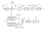
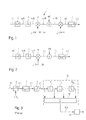
- FIG. 1 shows an expanded block circuit diagram of the transmission system
- FIG. 2 shows a reduced block circuit diagram of the transmission system
- FIG. 3 shows a circuit diagram of the device for clock synchronisation according to the prior art
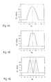
- FIGS. 4A , 4 B show a frequency response of the transmission filter for a PAM, QPSK or ⁇ /4-QPSK signal with a roll-off factor of 1 and 0.5;
- FIGS. 4C , 4 D show a frequency response of the overall transmission path with a roll-off factor of 1 and 0.5;
- FIG. 5 shows a frequency response of the transmission filter for a VSB signal
- FIG. 6 shows a block circuit diagram of a first embodiment of the device according to the invention for clock synchronisation with a VSB signal
- FIG. 7 shows a flow chart of a first embodiment of the method according to the invention for clock synchronisation with a VSB signal
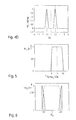
- FIG. 8 shows a frequency response of the estimation filter consisting of receiver filter and pre-filter
- FIG. 9 shows a block circuit diagram of a second embodiment of the device according to the invention for clock synchronisation with a VSB signal.
- FIG. 10 shows a flow chart of a second embodiment of the method according to the invention for clock synchronisation with a VSB signal.
- clock synchronisation with a QPSK signal using maximum-likelihood estimation is described as the prior art, so that the knowledge obtained can be transferred as an inventive step to clock synchronisation with a VSB signal.
- the starting point is a complex baseband model of a transmission system for time-continuous complex signals, of which the expanded block circuit diagram is shown in FIG. 1 .
- the complex symbol sequence s(t) of a PAM, QPSK or ⁇ /4 QPSK signal to be transmitted as shown in equation (1) is connected to the input of the transmission system 1 :
- a R (n) and a I (n) represent symbol values for the in-phase and quadrature components of the PAM, QPSK or ⁇ /4 QPSK transmitted signal to be generated, which can assume, for example, the real values ⁇ s i ⁇ of the symbol alphabet.
- the symbol sequences of the in-phase and quadrature components respectively are periodic with regard to the symbol length T s .
- the symbol sequence s(t) to be transmitted is convoluted in the transmitter filter 2 with its impulse response h s (t) and supplies the filtered symbol sequence s F (t) at the output of the transmitter filter 2 according to equation (2):
- the subsequent lag element 3 models the timing offset ⁇ T occurring as a result of absent or inadequate synchronisation between the transmitter and receiver, which is derived from a timing offset ⁇ to be determined by the method according to the invention or the device according to the invention.
- the timing offset ⁇ in this context can assume positive and negative values, typically between ⁇ 0.5.
- the filtered symbol sequence s ⁇ (t) is therefore derived according to equation (3):
- the lag-laden, filtered symbol sequence s ⁇ (t) is mixed with a complex carrier signal e j(2 ⁇ (f T + ⁇ f)t+ ⁇ ) to form a PAM, QPSK or ⁇ /4 QPSK modulated transmitted signal s HF (t).
- the carrier signal e j(2 ⁇ (f T + ⁇ f)t+ ⁇ ) has a carrier frequency f T , which provides a frequency offset ⁇ f and phase offset ⁇ as a result of defective carrier-frequency synchronisation.
- AWGN additive white Gaussian noise
- the PAM, QPSK or ⁇ /4 QPSK modulated received signal r HF (t) with superimposed noise n(t) is mixed down into the baseband with the carrier signal e ⁇ j2 ⁇ f T t in a demodulator, which is modelled as the multiplier 5 in FIG. 1 .
- the de-modulated received signal r(t) at the output of the demodulator 5 which contains an in-phase and quadrature symbol sequence distorted with the frequency offset and phase offset of the carrier signal, is therefore derived according to equation (7):
- the transmitted signal s(t) with the additively superimposed, additive white Gaussian noise n(t) according to the reduced block circuit diagram in FIG. 2 is received in the receiver as a received signal r(t), which corresponds to the received signal according to equation (7) of the expanded block circuit diagram according to FIG. 1 .
- the received signal r(t) is convoluted in an estimation filter 8 according to equation (9) with its impulse response h EST (t) and leads to the signal v(t) at the output of the estimation filter 8 , which represents a filtered in-phase and quadrature symbol sequence distorted with regard to signal error, frequency offset and phase offset:
- v ( t ) r ( t )* h EST ( t ) (9)
- u _ ⁇ v ⁇ ⁇ ⁇ u v transmitted in the observation period, is described as a modulus-error-squared, integrated over the observation period T 0 between the registered, noise-laden received signal r(t) and the ideal, noise-free, modelled transmitted signal s (t) subject to the sought timing offset ⁇ .
- u ) In order to neutralise the likelihood functioning L( ⁇ ) from the symbol values u transmitted in the time interval T 0 , the conditional likelihood function L( ⁇
- the maximum-likelihood estimation can, in principle, be implemented within the framework of a simplified model for clock recovery over a limited number of symbols with an infinitely long observation time T 0 or within the framework of a more realistic model for clock recovery over an unlimited number of symbols with a limited observation time T 0 .
- the simplified model is presented here.
- an integration of the modiouss-error squared over an infinite integration period is derived according to equation (12) for the mathematical relationship of the conditional likelihood function L( ⁇
- Equation (13) With a limited symbol number N, the modelled transmitted signal s (t, u , ⁇ ) according to equation (13) is described, by way of deviation from equation (3), as a multiplicatively linked Dirac comb with the symbol duration T s , and the symbol values u V , which is convoluted with the impulse response h s (t) of the transmitter filter 3 .
- equation (15) Taking into consideration the scaling of the transmitter filter 3 presented in equation (14), the mathematical context described in equation (15) is derived for the integral of the squared, modelled transmitted signal s 2 (t, u , ⁇ ):
- Equation (16) The mathematical context shown in equation (16) is derived for the integral of the product of the received signal and the modelled transmitted signal r(t) ⁇ s (t, u , ⁇ ):
- equation (18) applies for the interconnected distribution density function p a ( u ):
- the log likelihood function l( ⁇ ) can be interpreted from a filtering of the received signal r(t) with an estimation filter—signal e(nT s + ⁇ T s )—, a nonlinear signal processing—inverted exponential function, integration, logarithm function—and an averaging—summation—.
- the nonlinear signal-processing function can be approximated by a modulus squaring, as shown in [1].
- FIG. 3 The block circuit diagram presented in FIG. 3 of a device for determining the timing offset ⁇ for the clock synchronisation of a PAM, QPSK and/or ⁇ /4 QPSK signal on the basis of a maximum-likelihood estimation, which represents the prior art, is obtained in the above manner.
- the received signal r(t) is sampled in a sampling and holding element 8 at a sampling rate f A , which is increased by comparison with the symbol frequency f s , of the received signal r(t) by the oversampling factor os.
- the transmitter filter 2 according to equation (21) has a frequency spectrum H s (f), which corresponds to a cosine filter with a roll-off factor r
- the combined frequency spectrum H EST (f) of the estimation filter 7 according to equation (22) must be designed dependent upon the frequency spectrum H s (f) of the transmitter filter 2 , in order to minimise data-dependent jitter in the received signal r(t).
- H s ⁇ ( f ) ⁇ 1 für ⁇ ⁇ ⁇ f ⁇ ⁇ f S 2 cos ⁇ [ ⁇ ⁇ ⁇ f ⁇ 2 ⁇ rf S - ⁇ ⁇ ( 1 - r ) 4 ⁇ r ] für ⁇ ⁇ ( 1 - r ) ⁇ f S 2 ⁇ ⁇ f ⁇ ⁇ ( 1 + r ) ⁇ f S 2 0 für ⁇ ⁇ ( 1 + r ) ⁇ f S 2 ⁇ ⁇ f ⁇ ( 21 )
- H EST ⁇ ( f ) ⁇ H S ⁇ ( f - f S ) + H S ⁇ ( f + f S ) für ⁇ ⁇ ⁇ f ⁇ ⁇ f S 2 ⁇ ( 1 + r ) d ⁇ ⁇ f S 0 fürf S ⁇
- the signal v(t) at the output of the estimation filter 7 can therefore be obtained in that the impulse response h s (t) of the transmitter filter 2 in the transmitter signal s NF (t) in the baseband according to equation (8) is replaced by the impulse response h GES (t) of the transmission system as a whole:
- h GES ⁇ ( t - ⁇ ⁇ ⁇ T S - nT S ) h GES ⁇ ⁇ 0 ⁇ ( t - ⁇ ⁇ ⁇ T S - nT S ) ⁇ ( - 1 ) n ⁇ cos ⁇ ( 2 ⁇ ⁇ ⁇ ⁇ f S 2 ⁇ ( t - ⁇ ⁇ ⁇ T S ) ) ( 26 )
- the signal q(t) is then averaged in an averaging filter 10 consisting of altogether N ⁇ 1 series-connected timing steps 11 1 , 11 2 , . . . , 11 N-1 , of which the outputs are supplied together with the input of the first timing step 11 1 to an adder 12 for summation of the signals q m (t) time-delayed respectively by a different number m of symbol lengths T s .
- the output signal m(t) of the averaging filter 10 can be obtained according to equation (32) by convolution of the signal q(t) with the impulse response h M (t) of the averaging filter 10 as presented in equation (31).
- the maximum of the averaged, modulus-squared, filtered received signal e(t), which corresponds, according to equation (20), to the maximum of the log likelihood function l( ⁇ ) and therefore to the sought timing offset ⁇ of the clock synchronisation, is determined.
- the values q(v) in a 2VSB signal represent the symbol sequence with the symbol alphabet ⁇ +1, ⁇ 1 ⁇ and the symbol duration T VSB , to which an additional pilot carrier is added.
- the transmitter filter for a VSB signal is also a cosine filter.
- the transmitter filter for a VSB signal is also a cosine filter.
- it is symmetrical to the frequency
- H SVSB ⁇ ( f ) H S ⁇ ( f - 1 4 ⁇ f Symbo ⁇ l_ ⁇ VSB ) ( 34 )
- h SVSB ⁇ ( t ) h S ⁇ ( t ) ⁇ e j ⁇ 2 ⁇ ⁇ 4 ⁇ T VSB ⁇ t ( 35 )
- the VSB signal s FVSB (t) disposed at the output of the transmitter filter 2 is therefore derived, by analogy with the case of a PAM, QPSK or ⁇ /4 QPSK-modulated signal in equation (2), from a convolution of the VSB signal according to equation (33) with the impulse response h SVSB (t) of the transmitter filter according to equation (35), and is described mathematically by equation (36), which is mathematically converted in several further stages:
- Equation (42) if the symbol duration T VSB according to equation (42) is set to be equal to half of the symbol duration T s of a PAM, QPSK or ⁇ /4 QPSK modulated signal, and if the cosine filter T s of a PAM, QPSK or ⁇ /4 QPSK modulated signal, frequency-displaced according to equation (34), is used as the transmitter filter of the VSB signal, a mathematical relationship for the modified baseband received signal r VSB ′(t) is derived, starting from equation (41), as shown in equation (43)
- ⁇ T VSB 1 2 ⁇ T S ( 42 )
- the mathematical term for the modified VSB baseband received signal r VSB ′(t) provides a quadrature component, which is phase-displaced by half a symbol length T s relative to the in-phase component, and therefore corresponds to an offset QPSK signal.
- the output signal v VSB ′(t) of the estimation filter 7 can be derived from the mathematical relationship in equation (25) for the output signal v(t) of the estimation filter 7 in the case of a PAM, QPSK or ⁇ /4 QPSK signal s(t) and is presented in equation (45):
- equation (46) By analogy with the impulse response h GES (t ⁇ T S ⁇ nT S ) in equation (26), the mathematical relationship in equation (46) can be determined for the impulse response
- h GES ⁇ ( t - ⁇ ⁇ ⁇ T S - T S 2 - nT S ) ⁇ h GES ⁇ ( t - ⁇ ⁇ ⁇ T S - T S 2 - nT S ) h GES ⁇ ⁇ 0 ⁇ ( t - ⁇ ⁇ ⁇ T S - T S 2 - nT S ) ⁇ ( - 1 ) n ⁇ sin ⁇ ( 2 ⁇ ⁇ ⁇ ⁇ f S 2 ⁇ ( t - ⁇ ⁇ ⁇ T S ⁇ ) ) ( 46 )
- equations (47) and (48) can be formulated on the basis of the mathematical terms in equations (26) and (46), and accordingly, in the presence of a modified VSB baseband received signal r VSB ′(t), the mathematical context for the output signal v VSB ′(t) of the estimation filter 7 can be transferred from equation (46) to equation (49).
- q VSB ′ ⁇ ( t ) R VSB 2 ⁇ ( t ) ⁇ cos 2 ⁇ ( 2 ⁇ ⁇ ⁇ ⁇ f S 2 ⁇ ( t - ⁇ ⁇ ⁇ T S ) ) + I VSB 2 ⁇ ( t ) ⁇ sin 2 ⁇ ( 2 ⁇ ⁇ ⁇ ⁇ f S 2 ⁇ ( t - ⁇ ⁇ ⁇ T S ) ) ( 50 )
- w ⁇ ( t - T S 2 - nT s ) is a function, which is limited to the range n ⁇ T s ⁇ t ⁇ T S ⁇ 2 ⁇ n ⁇ T s and which is even at the time
- equation (54) is obtained, in a first embodiment of the device for clock synchronisation of a VSB signal according to FIG. 5 , starting from equation (49) for the output signal q VSB ′′(t) after a pure squarer 16 :
- the signal q VSB ′′(t) represents a superimposition of three periodic signal components rotating respectively at the frequency f S + ⁇ f, ⁇ f S + ⁇ f and ⁇ f, each of which can be sampled with the Dirac pulses of the additively and multiplicatively linked combined terms R VSB (t) and I VSB (t)
- the signal q VSB ′′(t) therefore represents a periodic signal, which contains a discrete spectral pair ⁇ f s , of which the maximum can be determined with a maximum detector 13 and which supplies the sought timing offset ⁇ for the clock synchronisation of a VSB signal.
- the associated modulus of the spectrum which corresponds respectively to the convolution
- of a low pass filter symmetrical to the frequency f 0 relative to itself, is used by way of approximation, for the spectrum of the respective anticipated values E ⁇ R 0QPSK 2 (t) ⁇ and E ⁇ I 0QPSK 2 (t) ⁇ . Because of the band limitation of the low pass filter at the level of
- the convolutions are band-limited to
- ⁇ f s because of the squaring, so that the spectra of the anticipated values E ⁇ (R VSB (t)+I VSB (t)) 2 ⁇ and E ⁇ (R VSB (t) ⁇ I VSB (t)) 2 ⁇ are zero at the frequencies ⁇ i ⁇ f S with the exception of the equal component (i 0).
- the corresponding anticipated values E ⁇ (R VSB (t)+I VSB (t)) 2 ⁇ and E ⁇ (R VSB (t) ⁇ I VSB (t)) 2 ⁇ are therefore derived as constant values c 0 ′ and c 0 ′′.
- equation (56) the mathematical relationship in equation (56) is derived for the anticipated value E ⁇ q VSB ′′(t) ⁇ of the signal q VSB ′′(t):
- ⁇ 1 - 2 ⁇ ⁇ + 2 ⁇ ⁇ ⁇ ⁇ ⁇ ( 57 )
- ⁇ 2 2 ⁇ ⁇ + 2 ⁇ ⁇ ⁇ ⁇ ⁇ ( 58 )
- the first embodiment of the device according to the invention for clock synchronisation with a VSB signal implements a mirroring of the sideband on the VSB received signal r VSB (t) into the normal position at the carrier frequency f T in a unit for sideband mirroring 14 .
- a down mixer 15 the VSB received signal r VSB (t) is mixed down by means of a mixer signal
- the modified VSB received signal r VSB ′(t) is sampled in a downstream sampling and holding element 8 with an oversampling factor os.
- the sampled, modified VSB baseband received signal e VSB ′(t) is supplied to an estimation filter 7 to remove data-dependent jitter in the useful signal.
- the output signal v VSB (t) of the estimation filter 7 is then squared with a squarer 16 without a formation of the modulus.
- the squared and filtered VSB baseband received signal q VSB ′′(t) is then averaged, also by analogy with the averaging filter 12 of the prior art in FIG. 3 .
- the averaging according to the invention is subdivided into a first averaging filter 17 with the impulse response h MIT1 (t) and a second averaging filter 18 following later in the signal path with the impulse response h MIT2 (t).
- the separation of the averaging into two averaging steps is based on the fact that the two spectral lines of the squared, filtered received signal q VSB ′′(t), as shown in equation (56), are frequency-displaced relative to the two symbol frequencies ⁇ f s by the frequency offset 2 ⁇ f of the carrier signal.
- the bandwidth of the first averaging filter 17 must be designed to be appropriately broad.
- the impulse response h MIT1 (t) of the first averaging filter 17 is derived, by an analogy with the impulse response h M (t) of the averaging filter of the prior art, as shown in equation (34), from an averaging of a total of N symbols.
- the bandwidth of the first averaging filter 17 expanded in view of the above consideration, brings about a shortened averaging length.
- a second averaging filter 18 is introduced, which filters via a multiple of the averaging length of the first averaging filter 17 —altogether I ⁇ N symbol lengths.
- a first discrete Fourier transformer 19 following the first averaging filter 17 , the Fourier transform of the pre-filtered, squared and averaged received signal is determined at the frequency f s .
- the Fourier transform of the pre-filtered, squared and averaged received signal is calculated in a similar manner at the frequency ⁇ f s , in a second discrete Fourier transformer 20 .
- the Fourier transforms of the pre-filtered, squared and averaged received signal at the frequency f s is conjugated with regard to its phase in a downstream conjugator 21 .
- the conjugated Fourier transform of the pre-filtered, squared and averaged received signal at the frequency f s is multiplied in a multiplier 22 by the Fourier transform of the pre-filtered, squared and averaged received signal at the frequency ⁇ f s .
- the multiplier 22 is followed by the second averaging filter 18 mentioned above with the impulse response h MIT2 (t) according to equation (60).
- the second averaging filter 18 is used to remove further interference.
- the timing offset ⁇ is determined by argument formation—determination of the phase of the two Fourier transforms of the pre-filtered, squared and averaged received signal q VSB ′′(t) multiplied together—at the two frequencies ⁇ f s and scaled by the factor 1 ⁇ 4 ⁇ .
- the associated first embodiment of the method according to the invention for clock synchronisation with a VSB signal implements a mirroring of the sideband of the VSB baseband received signal r VSB (t) by the carrier frequency f T from an inverted position into a normal position, if the sideband is disposed in the inverted position.
- the VSB baseband received signal r VSB (t) is mixed down according to the invention with a mixer signal
- the modified VSB baseband received signal r VSB ′(t) is oversampled in a sampling and holding element 8 with an oversampling factor os of 8, in order to satisfy the Nyquist condition by frequency doubling on the basis of squaring and multiplication.
- an estimation filtering of the sampled, modified VSB baseband received signal e VSB ′(t) takes place in an estimation filter 7 according to equation (45) or respectively (49).
- the transmission function H EST (f) of the estimation filter 7 according to equation (22) is presented in FIG. 8 .
- the filtered, sampled and squared received signal q VSB ′′(t) is averaged in the subsequent procedural stage S 60 in a first averaging filter 17 according to equation (31) over a total of N symbol lengths.
- the next procedural stage S 70 comprises the determination of the discrete Fourier transform Q VSB ′′(f) respectively at the frequencies ⁇ f s in the first and second discrete Fourier transformer 19 and 20 .
- the conjugated Fourier transform Q VSB ′′*(fs) at the frequency f S is multiplied by the Fourier transform Q VSB ′′( ⁇ f S ) in a multiplier 22 at the frequency ⁇ f s in the subsequent procedural stage S 80 .
- the argument of the two Fourier transforms Q VSB ′′*(f S ) and Q VSB ′′( ⁇ f S ) multiplied with one another and averaged is determined, and a scaling with a scaling factor 1 ⁇ 4 ⁇ is carried out to determine the timing offset ⁇ .
- FIG. 9 shows a second embodiment of the device according to the invention for clock synchronisation with a VSB signal. Identical functional units to those in the first embodiment shown in FIG. 6 have been indicated with the same reference numbers.
- the second embodiment of the device according to the invention for clock synchronisation with a VSB signal shown in FIG. 9 is identical, in its functional structure along the signal path as far as the squarer 16 , to the first embodiment shown in FIG. 6 .
- the averaging in the first averaging filter and the discrete Fourier transformation in the first and second discrete Fourier transformer including the conjugation in the conjugator are exchanged with one another in the second embodiment.
- the squarer is followed by the conjugator 21 for the conjugation of the filtered, sampled and squared received signal q VSB ′′(t), with a first discrete Fourier transformer 19 for the implementation of the discrete Fourier transformation of the filtered, sampled, squared and conjugated received signal q VSB ′′(t) at the frequency f S and parallel to this, a second discrete Fourier transformer 20 for the implementation of the discrete Fourier transformation of the filtered, sampled and squared received signal q VSB ′′(t) at the frequency ⁇ f S
- the first averaging filter 17 of the first embodiment is connected as a first averaging filter 17 A and 17 B respectively downstream of the first and second discrete Fourier transformer 19 and 24 for the implementation of the first averaging of the two discrete Fourier transforms Q VSB ′′*(f S ) and Q VSB ′′( ⁇ f S ).
- the further functional structure in the signal path of the second embodiment corresponds to the functional structure of the first embodiment.
- FIG. 10 The flow chart for the associated method according to the invention for clock synchronisation with a VSB signal is presented in FIG. 10 .
- the procedural stages S 115 to S 150 and S 190 to S 210 of the second embodiment are identical to the corresponding procedural stages S 10 to S 50 and S 90 to S 110 of the first embodiment shown in FIG. 7 and will not be explained in any further detail below.
- the filtered, sampled and squared received signal q VSB ′′(t) is conjugated in a conjugator 21 .
- the Fourier transforms Q VSB ′′*(f S ) at the frequency f S and Q VSB ′′( ⁇ f S ) at the frequency ⁇ f S are calculated respectively in a first and second discrete Fourier transformer 19 and 20 from the conjugated, filtered, sampled and squared received signal q VSB ′′(t) and the un-conjugated, filtered, sampled and squared received signal q VSB ′′(t).
- the first averaging of the two discrete Fourier transforms Q VSB ′′*(f S ) at the frequency f s and Q VSB ′′( ⁇ f S ) at the frequency ⁇ f s takes place according to equation (31) in a first averaging filter 17 A and 17 B respectively.
- VSB signals with higher-value symbol alphabet for example, 8VSB signals and 16VSB signals—are also covered by the invention.
- the invention also covers VSB signals without a pilot carrier.
Abstract
Description
n(t)=n R(t)+j·n I(t) (5)
r HF(t)=s HF(t)+n(t) (6)
v(t)=r(t)*h EST(t) (9)
transmitted in the observation period, is described as a modulus-error-squared, integrated over the observation period T0 between the registered, noise-laden received signal r(t) and the ideal, noise-free, modelled transmitted signal
[beliebig=random; für=for]
which is frequency-displaced respectively by
wherein f is the symbol frequency fsVSB of the VSB signal inverse to the symbol period. Its transmission function HsVSB(f) is therefore derived from a displacement of the transmission function Hs(f) of a PAM, QPSK or π/4 QPSK modulated signal according to equation (21) by the frequency
in the sense of equation (34) and
in equation (36),
in equation (36) can be subdivided according to equation (40) into a partial sum for even-numbered v=2n and respectively odd numbered v=2n+1:
if the symbol duration TVSB according to equation (42) is set to be equal to half of the symbol duration Ts of a PAM, QPSK or π/4 QPSK modulated signal, and if the cosine filter Ts of a PAM, QPSK or π/4 QPSK modulated signal, frequency-displaced according to equation (34), is used as the transmitter filter of the VSB signal, a mathematical relationship for the modified baseband received signal rVSB′(t) is derived, starting from equation (41), as shown in equation (43)
and the fact that the symbol alphabet of a modified 2VSB signal contains only the values {±1}, which do not correlate with one another over the individual sampling times nTs. As a result of the absence of a correlation, the individual products aR(iTs)·aR(jTs) and respectively aj(iTs)·aI(jTs) cancel each other out at different sampling times iTs and jTs respectively, while the products aR 2(iTs) and aI 2(iTs) each have the value +1 at the same sampling time iTs.
the equation (51) can be converted to the equation (52) for the signal E{qVSB′(t)}:
and which is even at the time t−εTS=n·Ts; and at the same time, for all n, the respective auxiliary function
is a function, which is limited to the range n·Ts≦t−εTS≦2·n·Ts and which is even at the time
a constant function is derived by superimposing all auxiliary functions w(t−nTs) and
for the anticipated value E{qVSB′(t)} of the signal qVSB′(t) according to equation (53), and the determination of the timing offset ε of the clock synchronisation of a VSB modulated signal via a detection of a maximum according to the prior art is dispensed with.
E{q VSB′(t)}=const. (53)
and
the mathematical relationship for the signal qVSB″(t) in equation (54) can be transformed according to equation (55).
the result of the convolution is band-limited to |f|≦fs, so that the spectrum of the respective anticipated values E{RVSB 2(t)} and E{IVSB 2(t)} is zero at all relevant frequencies ±i·fS (i: integer factor) with the exception of the equal component (i=0). The corresponding anticipated values E{RVSB 2(t)} of the combined term RVSB 2(t) and E{IVSB 2(t) of the combined term IVSB 2(t) are therefore derived taking into consideration equation (50) and (51) respectively as a constant factor c0, which corresponds to the modulus of the result of the convolution |HGES0(f=0)|*|HGES0(f=0)| at the
by the
by the
Claims (26)
Applications Claiming Priority (4)
| Application Number | Priority Date | Filing Date | Title |
|---|---|---|---|
| DE102004059956 | 2004-12-13 | ||
| DEGER102004059956.4 | 2004-12-13 | ||
| DE102004059956.4 | 2004-12-13 | ||
| DE102004059956A DE102004059956B4 (en) | 2004-12-13 | 2004-12-13 | Method and apparatus for clock synchronization in a vestigial sideband modulated transmission signal |
Publications (3)
| Publication Number | Publication Date |
|---|---|
| US20060208786A1 US20060208786A1 (en) | 2006-09-21 |
| US20070222495A2 US20070222495A2 (en) | 2007-09-27 |
| US7778359B2 true US7778359B2 (en) | 2010-08-17 |
Family
ID=36500250
Family Applications (1)
| Application Number | Title | Priority Date | Filing Date |
|---|---|---|---|
| US11/302,320 Expired - Fee Related US7778359B2 (en) | 2004-12-13 | 2005-12-13 | Method and device for clock synchronisation with a vestigial-sideband-modulated transmitted signal |
Country Status (2)
| Country | Link |
|---|---|
| US (1) | US7778359B2 (en) |
| DE (1) | DE102004059956B4 (en) |
Families Citing this family (5)
| Publication number | Priority date | Publication date | Assignee | Title |
|---|---|---|---|---|
| DE102004061899A1 (en) * | 2004-09-28 | 2006-03-30 | Rohde & Schwarz Gmbh & Co. Kg | Method and apparatus for clock synchronization in an offset QPSK-modulated transmission signal |
| DE102005015835B4 (en) * | 2004-12-13 | 2008-04-24 | Rohde & Schwarz Gmbh & Co. Kg | Method and apparatus for carrier frequency synchronization of a vestigial sideband modulated signal |
| JP5126204B2 (en) * | 2009-11-05 | 2013-01-23 | セイコーエプソン株式会社 | Frequency conversion circuit |
| WO2018035763A1 (en) * | 2016-08-24 | 2018-03-01 | 深圳天珑无线科技有限公司 | Symbol rate estimation method and device |
| US10200071B1 (en) * | 2017-08-07 | 2019-02-05 | Kratos Integral Holdings, Llc | System and method for interference reduction in radio communications |
Citations (10)
| Publication number | Priority date | Publication date | Assignee | Title |
|---|---|---|---|---|
| US4338579A (en) * | 1980-07-30 | 1982-07-06 | Communications Satelite Corp. | Frequency shift offset quadrature modulation and demodulation |
| US5832046A (en) | 1996-01-25 | 1998-11-03 | Northern Telecom Limited | Timing tracking in communications systems |
| US5870443A (en) * | 1997-03-19 | 1999-02-09 | Hughes Electronics Corporation | Symbol timing recovery and tracking method for burst-mode digital communications |
| US5894334A (en) * | 1994-03-21 | 1999-04-13 | Rca Thomson Licensing Corporation | Carrier recovery system for a vestigial sideband signal |
| WO1999021323A2 (en) | 1997-10-20 | 1999-04-29 | Wireless Facilities Inc. | Wireless multimedia carrier system |
| WO1999060746A1 (en) | 1998-05-18 | 1999-11-25 | Sarnoff Corporation | Method and apparatus for performing phase detection and timing recovery for a vestigial sideband receiver |
| US20010031022A1 (en) * | 1996-10-11 | 2001-10-18 | Paul Petrus | Method for reference signal generation in the presence of frequency offsets in a communications station with spatial processing |
| US6411659B1 (en) * | 1998-11-03 | 2002-06-25 | Broadcom Corporation | Timing recovery using the pilot signal in high definition TV |
| US6842495B1 (en) * | 1998-11-03 | 2005-01-11 | Broadcom Corporation | Dual mode QAM/VSB receiver |
| US20070263742A1 (en) * | 2004-09-28 | 2007-11-15 | Rohde & Schwarz Gmbh & Co. Kg | Method and Apparatus for Clock-Pulse Synchronization with an Offset Qpsk-Modulated Transmission Signal |
-
2004
- 2004-12-13 DE DE102004059956A patent/DE102004059956B4/en not_active Expired - Fee Related
-
2005
- 2005-12-13 US US11/302,320 patent/US7778359B2/en not_active Expired - Fee Related
Patent Citations (10)
| Publication number | Priority date | Publication date | Assignee | Title |
|---|---|---|---|---|
| US4338579A (en) * | 1980-07-30 | 1982-07-06 | Communications Satelite Corp. | Frequency shift offset quadrature modulation and demodulation |
| US5894334A (en) * | 1994-03-21 | 1999-04-13 | Rca Thomson Licensing Corporation | Carrier recovery system for a vestigial sideband signal |
| US5832046A (en) | 1996-01-25 | 1998-11-03 | Northern Telecom Limited | Timing tracking in communications systems |
| US20010031022A1 (en) * | 1996-10-11 | 2001-10-18 | Paul Petrus | Method for reference signal generation in the presence of frequency offsets in a communications station with spatial processing |
| US5870443A (en) * | 1997-03-19 | 1999-02-09 | Hughes Electronics Corporation | Symbol timing recovery and tracking method for burst-mode digital communications |
| WO1999021323A2 (en) | 1997-10-20 | 1999-04-29 | Wireless Facilities Inc. | Wireless multimedia carrier system |
| WO1999060746A1 (en) | 1998-05-18 | 1999-11-25 | Sarnoff Corporation | Method and apparatus for performing phase detection and timing recovery for a vestigial sideband receiver |
| US6411659B1 (en) * | 1998-11-03 | 2002-06-25 | Broadcom Corporation | Timing recovery using the pilot signal in high definition TV |
| US6842495B1 (en) * | 1998-11-03 | 2005-01-11 | Broadcom Corporation | Dual mode QAM/VSB receiver |
| US20070263742A1 (en) * | 2004-09-28 | 2007-11-15 | Rohde & Schwarz Gmbh & Co. Kg | Method and Apparatus for Clock-Pulse Synchronization with an Offset Qpsk-Modulated Transmission Signal |
Also Published As
| Publication number | Publication date |
|---|---|
| DE102004059956B4 (en) | 2008-09-11 |
| US20070222495A2 (en) | 2007-09-27 |
| DE102004059956A1 (en) | 2006-06-14 |
| US20060208786A1 (en) | 2006-09-21 |
Similar Documents
| Publication | Publication Date | Title |
|---|---|---|
| US8090320B2 (en) | Strong signal tolerant OFDM receiver and receiving methods | |
| EP1269706B1 (en) | Method to compensate for phase errors in multi-carrier signals | |
| JP3017041B2 (en) | Automatic frequency control method and device | |
| US8055234B2 (en) | Methods and apparatus for suppressing strong-signal interference in low-IF receivers | |
| US7620124B2 (en) | Direct conversion receiver and receiving method | |
| EP0616745A1 (en) | Timing and automatic frequency control of digital receiver using the cyclic properties of a non-linear operation | |
| JPH03188738A (en) | System and apparatus for psk signal demodulation | |
| US7778359B2 (en) | Method and device for clock synchronisation with a vestigial-sideband-modulated transmitted signal | |
| US7970071B2 (en) | Method and device for synchronizing the carrier frequency of an offset quadrature phase-modulated signal | |
| US7869534B2 (en) | Method and apparatus for clock-pulse synchronization with an offset QPSK-modulated transmission signal | |
| US7433415B2 (en) | System and method for transmission and reception of QAM signals at low signal to noise ratio | |
| US7587003B2 (en) | Method and device for carrier-frequency synchronization of a vestigial-sideband-modulated signal | |
| US11962443B2 (en) | Frequency offset estimation | |
| US7277501B2 (en) | Data receiving device | |
| US6859507B2 (en) | Method and apparatus for correcting a signal | |
| JP3873078B2 (en) | Timing extracting apparatus and method, and demodulating apparatus including the timing extracting apparatus | |
| JP3643109B2 (en) | Data receiving device | |
| JPH0583314A (en) | Demodulation circuit | |
| Gunnam et al. | New optimizations for carrier synchronization in single carrier systems | |
| Jankovic et al. | Extraction of in-phase and quadrature components by IF-sampling | |
| JP2943803B1 (en) | Receiver | |
| JPH09326838A (en) | Automatic frequency control circuit | |
| Chi et al. | A fully digital feedforward demodulator for vector signal analyzers | |
| JPH0787056A (en) | Digital demodulator | |
| JPH03101344A (en) | Frequency discriminator |
Legal Events
| Date | Code | Title | Description |
|---|---|---|---|
| AS | Assignment |
Owner name: ROHDE & SCHWARTZ GMBH & CO. KG, GERMANY Free format text: ASSIGNMENT OF ASSIGNORS INTEREST;ASSIGNORS:PLIQUETT, JOCHEN;REICHERT, THOMAS;REEL/FRAME:017535/0988 Effective date: 20050812 |
|
| STCF | Information on status: patent grant |
Free format text: PATENTED CASE |
|
| FEPP | Fee payment procedure |
Free format text: PAYOR NUMBER ASSIGNED (ORIGINAL EVENT CODE: ASPN); ENTITY STATUS OF PATENT OWNER: LARGE ENTITY |
|
| FPAY | Fee payment |
Year of fee payment: 4 |
|
| MAFP | Maintenance fee payment |
Free format text: PAYMENT OF MAINTENANCE FEE, 8TH YEAR, LARGE ENTITY (ORIGINAL EVENT CODE: M1552) Year of fee payment: 8 |
|
| FEPP | Fee payment procedure |
Free format text: MAINTENANCE FEE REMINDER MAILED (ORIGINAL EVENT CODE: REM.); ENTITY STATUS OF PATENT OWNER: LARGE ENTITY |
|
| LAPS | Lapse for failure to pay maintenance fees |
Free format text: PATENT EXPIRED FOR FAILURE TO PAY MAINTENANCE FEES (ORIGINAL EVENT CODE: EXP.); ENTITY STATUS OF PATENT OWNER: LARGE ENTITY |
|
| STCH | Information on status: patent discontinuation |
Free format text: PATENT EXPIRED DUE TO NONPAYMENT OF MAINTENANCE FEES UNDER 37 CFR 1.362 |
|
| FP | Lapsed due to failure to pay maintenance fee |
Effective date: 20220817 |