US7790504B2 - Integrated circuit package system - Google Patents
Integrated circuit package system Download PDFInfo
- Publication number
- US7790504B2 US7790504B2 US11/276,727 US27672706A US7790504B2 US 7790504 B2 US7790504 B2 US 7790504B2 US 27672706 A US27672706 A US 27672706A US 7790504 B2 US7790504 B2 US 7790504B2
- Authority
- US
- United States
- Prior art keywords
- stud bump
- forming
- integrated circuit
- providing
- compression via
- Prior art date
- Legal status (The legal status is an assumption and is not a legal conclusion. Google has not performed a legal analysis and makes no representation as to the accuracy of the status listed.)
- Active, expires
Links
Images


Classifications
-
- H—ELECTRICITY
- H01—ELECTRIC ELEMENTS
- H01L—SEMICONDUCTOR DEVICES NOT COVERED BY CLASS H10
- H01L23/00—Details of semiconductor or other solid state devices
- H01L23/48—Arrangements for conducting electric current to or from the solid state body in operation, e.g. leads, terminal arrangements ; Selection of materials therefor
- H01L23/488—Arrangements for conducting electric current to or from the solid state body in operation, e.g. leads, terminal arrangements ; Selection of materials therefor consisting of soldered or bonded constructions
- H01L23/498—Leads, i.e. metallisations or lead-frames on insulating substrates, e.g. chip carriers
- H01L23/49811—Additional leads joined to the metallisation on the insulating substrate, e.g. pins, bumps, wires, flat leads
-
- H—ELECTRICITY
- H01—ELECTRIC ELEMENTS
- H01L—SEMICONDUCTOR DEVICES NOT COVERED BY CLASS H10
- H01L23/00—Details of semiconductor or other solid state devices
- H01L23/12—Mountings, e.g. non-detachable insulating substrates
- H01L23/13—Mountings, e.g. non-detachable insulating substrates characterised by the shape
-
- H—ELECTRICITY
- H01—ELECTRIC ELEMENTS
- H01L—SEMICONDUCTOR DEVICES NOT COVERED BY CLASS H10
- H01L23/00—Details of semiconductor or other solid state devices
- H01L23/48—Arrangements for conducting electric current to or from the solid state body in operation, e.g. leads, terminal arrangements ; Selection of materials therefor
- H01L23/488—Arrangements for conducting electric current to or from the solid state body in operation, e.g. leads, terminal arrangements ; Selection of materials therefor consisting of soldered or bonded constructions
- H01L23/498—Leads, i.e. metallisations or lead-frames on insulating substrates, e.g. chip carriers
- H01L23/49833—Leads, i.e. metallisations or lead-frames on insulating substrates, e.g. chip carriers the chip support structure consisting of a plurality of insulating substrates
-
- H—ELECTRICITY
- H01—ELECTRIC ELEMENTS
- H01L—SEMICONDUCTOR DEVICES NOT COVERED BY CLASS H10
- H01L24/00—Arrangements for connecting or disconnecting semiconductor or solid-state bodies; Methods or apparatus related thereto
- H01L24/01—Means for bonding being attached to, or being formed on, the surface to be connected, e.g. chip-to-package, die-attach, "first-level" interconnects; Manufacturing methods related thereto
- H01L24/10—Bump connectors ; Manufacturing methods related thereto
- H01L24/11—Manufacturing methods
-
- H—ELECTRICITY
- H01—ELECTRIC ELEMENTS
- H01L—SEMICONDUCTOR DEVICES NOT COVERED BY CLASS H10
- H01L24/00—Arrangements for connecting or disconnecting semiconductor or solid-state bodies; Methods or apparatus related thereto
- H01L24/01—Means for bonding being attached to, or being formed on, the surface to be connected, e.g. chip-to-package, die-attach, "first-level" interconnects; Manufacturing methods related thereto
- H01L24/10—Bump connectors ; Manufacturing methods related thereto
- H01L24/12—Structure, shape, material or disposition of the bump connectors prior to the connecting process
- H01L24/13—Structure, shape, material or disposition of the bump connectors prior to the connecting process of an individual bump connector
-
- H—ELECTRICITY
- H01—ELECTRIC ELEMENTS
- H01L—SEMICONDUCTOR DEVICES NOT COVERED BY CLASS H10
- H01L24/00—Arrangements for connecting or disconnecting semiconductor or solid-state bodies; Methods or apparatus related thereto
- H01L24/01—Means for bonding being attached to, or being formed on, the surface to be connected, e.g. chip-to-package, die-attach, "first-level" interconnects; Manufacturing methods related thereto
- H01L24/26—Layer connectors, e.g. plate connectors, solder or adhesive layers; Manufacturing methods related thereto
- H01L24/31—Structure, shape, material or disposition of the layer connectors after the connecting process
- H01L24/32—Structure, shape, material or disposition of the layer connectors after the connecting process of an individual layer connector
-
- H—ELECTRICITY
- H01—ELECTRIC ELEMENTS
- H01L—SEMICONDUCTOR DEVICES NOT COVERED BY CLASS H10
- H01L24/00—Arrangements for connecting or disconnecting semiconductor or solid-state bodies; Methods or apparatus related thereto
- H01L24/71—Means for bonding not being attached to, or not being formed on, the surface to be connected
- H01L24/72—Detachable connecting means consisting of mechanical auxiliary parts connecting the device, e.g. pressure contacts using springs or clips
-
- H—ELECTRICITY
- H01—ELECTRIC ELEMENTS
- H01L—SEMICONDUCTOR DEVICES NOT COVERED BY CLASS H10
- H01L24/00—Arrangements for connecting or disconnecting semiconductor or solid-state bodies; Methods or apparatus related thereto
- H01L24/80—Methods for connecting semiconductor or other solid state bodies using means for bonding being attached to, or being formed on, the surface to be connected
- H01L24/81—Methods for connecting semiconductor or other solid state bodies using means for bonding being attached to, or being formed on, the surface to be connected using a bump connector
-
- H—ELECTRICITY
- H01—ELECTRIC ELEMENTS
- H01L—SEMICONDUCTOR DEVICES NOT COVERED BY CLASS H10
- H01L24/00—Arrangements for connecting or disconnecting semiconductor or solid-state bodies; Methods or apparatus related thereto
- H01L24/90—Methods for connecting semiconductor or solid state bodies using means for bonding not being attached to, or not being formed on, the body surface to be connected, e.g. pressure contacts using springs or clips
-
- H—ELECTRICITY
- H01—ELECTRIC ELEMENTS
- H01L—SEMICONDUCTOR DEVICES NOT COVERED BY CLASS H10
- H01L25/00—Assemblies consisting of a plurality of individual semiconductor or other solid state devices ; Multistep manufacturing processes thereof
- H01L25/03—Assemblies consisting of a plurality of individual semiconductor or other solid state devices ; Multistep manufacturing processes thereof all the devices being of a type provided for in the same subgroup of groups H01L27/00 - H01L33/00, or in a single subclass of H10K, H10N, e.g. assemblies of rectifier diodes
- H01L25/04—Assemblies consisting of a plurality of individual semiconductor or other solid state devices ; Multistep manufacturing processes thereof all the devices being of a type provided for in the same subgroup of groups H01L27/00 - H01L33/00, or in a single subclass of H10K, H10N, e.g. assemblies of rectifier diodes the devices not having separate containers
- H01L25/065—Assemblies consisting of a plurality of individual semiconductor or other solid state devices ; Multistep manufacturing processes thereof all the devices being of a type provided for in the same subgroup of groups H01L27/00 - H01L33/00, or in a single subclass of H10K, H10N, e.g. assemblies of rectifier diodes the devices not having separate containers the devices being of a type provided for in group H01L27/00
- H01L25/0657—Stacked arrangements of devices
-
- H—ELECTRICITY
- H01—ELECTRIC ELEMENTS
- H01L—SEMICONDUCTOR DEVICES NOT COVERED BY CLASS H10
- H01L2224/00—Indexing scheme for arrangements for connecting or disconnecting semiconductor or solid-state bodies and methods related thereto as covered by H01L24/00
- H01L2224/01—Means for bonding being attached to, or being formed on, the surface to be connected, e.g. chip-to-package, die-attach, "first-level" interconnects; Manufacturing methods related thereto
- H01L2224/02—Bonding areas; Manufacturing methods related thereto
- H01L2224/04—Structure, shape, material or disposition of the bonding areas prior to the connecting process
- H01L2224/0401—Bonding areas specifically adapted for bump connectors, e.g. under bump metallisation [UBM]
-
- H—ELECTRICITY
- H01—ELECTRIC ELEMENTS
- H01L—SEMICONDUCTOR DEVICES NOT COVERED BY CLASS H10
- H01L2224/00—Indexing scheme for arrangements for connecting or disconnecting semiconductor or solid-state bodies and methods related thereto as covered by H01L24/00
- H01L2224/01—Means for bonding being attached to, or being formed on, the surface to be connected, e.g. chip-to-package, die-attach, "first-level" interconnects; Manufacturing methods related thereto
- H01L2224/02—Bonding areas; Manufacturing methods related thereto
- H01L2224/04—Structure, shape, material or disposition of the bonding areas prior to the connecting process
- H01L2224/05—Structure, shape, material or disposition of the bonding areas prior to the connecting process of an individual bonding area
- H01L2224/0554—External layer
- H01L2224/0555—Shape
- H01L2224/05552—Shape in top view
- H01L2224/05555—Shape in top view being circular or elliptic
-
- H—ELECTRICITY
- H01—ELECTRIC ELEMENTS
- H01L—SEMICONDUCTOR DEVICES NOT COVERED BY CLASS H10
- H01L2224/00—Indexing scheme for arrangements for connecting or disconnecting semiconductor or solid-state bodies and methods related thereto as covered by H01L24/00
- H01L2224/01—Means for bonding being attached to, or being formed on, the surface to be connected, e.g. chip-to-package, die-attach, "first-level" interconnects; Manufacturing methods related thereto
- H01L2224/02—Bonding areas; Manufacturing methods related thereto
- H01L2224/04—Structure, shape, material or disposition of the bonding areas prior to the connecting process
- H01L2224/05—Structure, shape, material or disposition of the bonding areas prior to the connecting process of an individual bonding area
- H01L2224/0554—External layer
- H01L2224/0556—Disposition
- H01L2224/05571—Disposition the external layer being disposed in a recess of the surface
-
- H—ELECTRICITY
- H01—ELECTRIC ELEMENTS
- H01L—SEMICONDUCTOR DEVICES NOT COVERED BY CLASS H10
- H01L2224/00—Indexing scheme for arrangements for connecting or disconnecting semiconductor or solid-state bodies and methods related thereto as covered by H01L24/00
- H01L2224/01—Means for bonding being attached to, or being formed on, the surface to be connected, e.g. chip-to-package, die-attach, "first-level" interconnects; Manufacturing methods related thereto
- H01L2224/10—Bump connectors; Manufacturing methods related thereto
- H01L2224/11—Manufacturing methods
- H01L2224/113—Manufacturing methods by local deposition of the material of the bump connector
- H01L2224/1133—Manufacturing methods by local deposition of the material of the bump connector in solid form
- H01L2224/1134—Stud bumping, i.e. using a wire-bonding apparatus
-
- H—ELECTRICITY
- H01—ELECTRIC ELEMENTS
- H01L—SEMICONDUCTOR DEVICES NOT COVERED BY CLASS H10
- H01L2224/00—Indexing scheme for arrangements for connecting or disconnecting semiconductor or solid-state bodies and methods related thereto as covered by H01L24/00
- H01L2224/01—Means for bonding being attached to, or being formed on, the surface to be connected, e.g. chip-to-package, die-attach, "first-level" interconnects; Manufacturing methods related thereto
- H01L2224/10—Bump connectors; Manufacturing methods related thereto
- H01L2224/12—Structure, shape, material or disposition of the bump connectors prior to the connecting process
- H01L2224/13—Structure, shape, material or disposition of the bump connectors prior to the connecting process of an individual bump connector
- H01L2224/13001—Core members of the bump connector
- H01L2224/1301—Shape
- H01L2224/13012—Shape in top view
-
- H—ELECTRICITY
- H01—ELECTRIC ELEMENTS
- H01L—SEMICONDUCTOR DEVICES NOT COVERED BY CLASS H10
- H01L2224/00—Indexing scheme for arrangements for connecting or disconnecting semiconductor or solid-state bodies and methods related thereto as covered by H01L24/00
- H01L2224/01—Means for bonding being attached to, or being formed on, the surface to be connected, e.g. chip-to-package, die-attach, "first-level" interconnects; Manufacturing methods related thereto
- H01L2224/10—Bump connectors; Manufacturing methods related thereto
- H01L2224/12—Structure, shape, material or disposition of the bump connectors prior to the connecting process
- H01L2224/13—Structure, shape, material or disposition of the bump connectors prior to the connecting process of an individual bump connector
- H01L2224/13001—Core members of the bump connector
- H01L2224/1301—Shape
- H01L2224/13016—Shape in side view
- H01L2224/13018—Shape in side view comprising protrusions or indentations
- H01L2224/13019—Shape in side view comprising protrusions or indentations at the bonding interface of the bump connector, i.e. on the surface of the bump connector
-
- H—ELECTRICITY
- H01—ELECTRIC ELEMENTS
- H01L—SEMICONDUCTOR DEVICES NOT COVERED BY CLASS H10
- H01L2224/00—Indexing scheme for arrangements for connecting or disconnecting semiconductor or solid-state bodies and methods related thereto as covered by H01L24/00
- H01L2224/01—Means for bonding being attached to, or being formed on, the surface to be connected, e.g. chip-to-package, die-attach, "first-level" interconnects; Manufacturing methods related thereto
- H01L2224/10—Bump connectors; Manufacturing methods related thereto
- H01L2224/12—Structure, shape, material or disposition of the bump connectors prior to the connecting process
- H01L2224/13—Structure, shape, material or disposition of the bump connectors prior to the connecting process of an individual bump connector
- H01L2224/13001—Core members of the bump connector
- H01L2224/13099—Material
- H01L2224/131—Material with a principal constituent of the material being a metal or a metalloid, e.g. boron [B], silicon [Si], germanium [Ge], arsenic [As], antimony [Sb], tellurium [Te] and polonium [Po], and alloys thereof
- H01L2224/13138—Material with a principal constituent of the material being a metal or a metalloid, e.g. boron [B], silicon [Si], germanium [Ge], arsenic [As], antimony [Sb], tellurium [Te] and polonium [Po], and alloys thereof the principal constituent melting at a temperature of greater than or equal to 950°C and less than 1550°C
- H01L2224/13144—Gold [Au] as principal constituent
-
- H—ELECTRICITY
- H01—ELECTRIC ELEMENTS
- H01L—SEMICONDUCTOR DEVICES NOT COVERED BY CLASS H10
- H01L2224/00—Indexing scheme for arrangements for connecting or disconnecting semiconductor or solid-state bodies and methods related thereto as covered by H01L24/00
- H01L2224/01—Means for bonding being attached to, or being formed on, the surface to be connected, e.g. chip-to-package, die-attach, "first-level" interconnects; Manufacturing methods related thereto
- H01L2224/10—Bump connectors; Manufacturing methods related thereto
- H01L2224/15—Structure, shape, material or disposition of the bump connectors after the connecting process
- H01L2224/16—Structure, shape, material or disposition of the bump connectors after the connecting process of an individual bump connector
- H01L2224/161—Disposition
- H01L2224/16151—Disposition the bump connector connecting between a semiconductor or solid-state body and an item not being a semiconductor or solid-state body, e.g. chip-to-substrate, chip-to-passive
- H01L2224/16221—Disposition the bump connector connecting between a semiconductor or solid-state body and an item not being a semiconductor or solid-state body, e.g. chip-to-substrate, chip-to-passive the body and the item being stacked
- H01L2224/16225—Disposition the bump connector connecting between a semiconductor or solid-state body and an item not being a semiconductor or solid-state body, e.g. chip-to-substrate, chip-to-passive the body and the item being stacked the item being non-metallic, e.g. insulating substrate with or without metallisation
- H01L2224/16237—Disposition the bump connector connecting between a semiconductor or solid-state body and an item not being a semiconductor or solid-state body, e.g. chip-to-substrate, chip-to-passive the body and the item being stacked the item being non-metallic, e.g. insulating substrate with or without metallisation the bump connector connecting to a bonding area disposed in a recess of the surface of the item
-
- H—ELECTRICITY
- H01—ELECTRIC ELEMENTS
- H01L—SEMICONDUCTOR DEVICES NOT COVERED BY CLASS H10
- H01L2224/00—Indexing scheme for arrangements for connecting or disconnecting semiconductor or solid-state bodies and methods related thereto as covered by H01L24/00
- H01L2224/01—Means for bonding being attached to, or being formed on, the surface to be connected, e.g. chip-to-package, die-attach, "first-level" interconnects; Manufacturing methods related thereto
- H01L2224/10—Bump connectors; Manufacturing methods related thereto
- H01L2224/15—Structure, shape, material or disposition of the bump connectors after the connecting process
- H01L2224/16—Structure, shape, material or disposition of the bump connectors after the connecting process of an individual bump connector
- H01L2224/161—Disposition
- H01L2224/16151—Disposition the bump connector connecting between a semiconductor or solid-state body and an item not being a semiconductor or solid-state body, e.g. chip-to-substrate, chip-to-passive
- H01L2224/16221—Disposition the bump connector connecting between a semiconductor or solid-state body and an item not being a semiconductor or solid-state body, e.g. chip-to-substrate, chip-to-passive the body and the item being stacked
- H01L2224/16225—Disposition the bump connector connecting between a semiconductor or solid-state body and an item not being a semiconductor or solid-state body, e.g. chip-to-substrate, chip-to-passive the body and the item being stacked the item being non-metallic, e.g. insulating substrate with or without metallisation
- H01L2224/16238—Disposition the bump connector connecting between a semiconductor or solid-state body and an item not being a semiconductor or solid-state body, e.g. chip-to-substrate, chip-to-passive the body and the item being stacked the item being non-metallic, e.g. insulating substrate with or without metallisation the bump connector connecting to a bonding area protruding from the surface of the item
-
- H—ELECTRICITY
- H01—ELECTRIC ELEMENTS
- H01L—SEMICONDUCTOR DEVICES NOT COVERED BY CLASS H10
- H01L2224/00—Indexing scheme for arrangements for connecting or disconnecting semiconductor or solid-state bodies and methods related thereto as covered by H01L24/00
- H01L2224/01—Means for bonding being attached to, or being formed on, the surface to be connected, e.g. chip-to-package, die-attach, "first-level" interconnects; Manufacturing methods related thereto
- H01L2224/10—Bump connectors; Manufacturing methods related thereto
- H01L2224/15—Structure, shape, material or disposition of the bump connectors after the connecting process
- H01L2224/16—Structure, shape, material or disposition of the bump connectors after the connecting process of an individual bump connector
- H01L2224/161—Disposition
- H01L2224/16151—Disposition the bump connector connecting between a semiconductor or solid-state body and an item not being a semiconductor or solid-state body, e.g. chip-to-substrate, chip-to-passive
- H01L2224/16221—Disposition the bump connector connecting between a semiconductor or solid-state body and an item not being a semiconductor or solid-state body, e.g. chip-to-substrate, chip-to-passive the body and the item being stacked
- H01L2224/16245—Disposition the bump connector connecting between a semiconductor or solid-state body and an item not being a semiconductor or solid-state body, e.g. chip-to-substrate, chip-to-passive the body and the item being stacked the item being metallic
-
- H—ELECTRICITY
- H01—ELECTRIC ELEMENTS
- H01L—SEMICONDUCTOR DEVICES NOT COVERED BY CLASS H10
- H01L2224/00—Indexing scheme for arrangements for connecting or disconnecting semiconductor or solid-state bodies and methods related thereto as covered by H01L24/00
- H01L2224/01—Means for bonding being attached to, or being formed on, the surface to be connected, e.g. chip-to-package, die-attach, "first-level" interconnects; Manufacturing methods related thereto
- H01L2224/26—Layer connectors, e.g. plate connectors, solder or adhesive layers; Manufacturing methods related thereto
- H01L2224/31—Structure, shape, material or disposition of the layer connectors after the connecting process
- H01L2224/32—Structure, shape, material or disposition of the layer connectors after the connecting process of an individual layer connector
- H01L2224/321—Disposition
- H01L2224/32151—Disposition the layer connector connecting between a semiconductor or solid-state body and an item not being a semiconductor or solid-state body, e.g. chip-to-substrate, chip-to-passive
- H01L2224/32221—Disposition the layer connector connecting between a semiconductor or solid-state body and an item not being a semiconductor or solid-state body, e.g. chip-to-substrate, chip-to-passive the body and the item being stacked
- H01L2224/32225—Disposition the layer connector connecting between a semiconductor or solid-state body and an item not being a semiconductor or solid-state body, e.g. chip-to-substrate, chip-to-passive the body and the item being stacked the item being non-metallic, e.g. insulating substrate with or without metallisation
-
- H—ELECTRICITY
- H01—ELECTRIC ELEMENTS
- H01L—SEMICONDUCTOR DEVICES NOT COVERED BY CLASS H10
- H01L2224/00—Indexing scheme for arrangements for connecting or disconnecting semiconductor or solid-state bodies and methods related thereto as covered by H01L24/00
- H01L2224/01—Means for bonding being attached to, or being formed on, the surface to be connected, e.g. chip-to-package, die-attach, "first-level" interconnects; Manufacturing methods related thereto
- H01L2224/42—Wire connectors; Manufacturing methods related thereto
- H01L2224/44—Structure, shape, material or disposition of the wire connectors prior to the connecting process
- H01L2224/45—Structure, shape, material or disposition of the wire connectors prior to the connecting process of an individual wire connector
- H01L2224/45001—Core members of the connector
- H01L2224/4501—Shape
- H01L2224/45012—Cross-sectional shape
- H01L2224/45015—Cross-sectional shape being circular
-
- H—ELECTRICITY
- H01—ELECTRIC ELEMENTS
- H01L—SEMICONDUCTOR DEVICES NOT COVERED BY CLASS H10
- H01L2224/00—Indexing scheme for arrangements for connecting or disconnecting semiconductor or solid-state bodies and methods related thereto as covered by H01L24/00
- H01L2224/01—Means for bonding being attached to, or being formed on, the surface to be connected, e.g. chip-to-package, die-attach, "first-level" interconnects; Manufacturing methods related thereto
- H01L2224/42—Wire connectors; Manufacturing methods related thereto
- H01L2224/44—Structure, shape, material or disposition of the wire connectors prior to the connecting process
- H01L2224/45—Structure, shape, material or disposition of the wire connectors prior to the connecting process of an individual wire connector
- H01L2224/45001—Core members of the connector
- H01L2224/45099—Material
- H01L2224/451—Material with a principal constituent of the material being a metal or a metalloid, e.g. boron (B), silicon (Si), germanium (Ge), arsenic (As), antimony (Sb), tellurium (Te) and polonium (Po), and alloys thereof
- H01L2224/45138—Material with a principal constituent of the material being a metal or a metalloid, e.g. boron (B), silicon (Si), germanium (Ge), arsenic (As), antimony (Sb), tellurium (Te) and polonium (Po), and alloys thereof the principal constituent melting at a temperature of greater than or equal to 950°C and less than 1550°C
- H01L2224/45144—Gold (Au) as principal constituent
-
- H—ELECTRICITY
- H01—ELECTRIC ELEMENTS
- H01L—SEMICONDUCTOR DEVICES NOT COVERED BY CLASS H10
- H01L2224/00—Indexing scheme for arrangements for connecting or disconnecting semiconductor or solid-state bodies and methods related thereto as covered by H01L24/00
- H01L2224/01—Means for bonding being attached to, or being formed on, the surface to be connected, e.g. chip-to-package, die-attach, "first-level" interconnects; Manufacturing methods related thereto
- H01L2224/42—Wire connectors; Manufacturing methods related thereto
- H01L2224/47—Structure, shape, material or disposition of the wire connectors after the connecting process
- H01L2224/48—Structure, shape, material or disposition of the wire connectors after the connecting process of an individual wire connector
- H01L2224/4805—Shape
- H01L2224/4809—Loop shape
- H01L2224/48091—Arched
-
- H—ELECTRICITY
- H01—ELECTRIC ELEMENTS
- H01L—SEMICONDUCTOR DEVICES NOT COVERED BY CLASS H10
- H01L2224/00—Indexing scheme for arrangements for connecting or disconnecting semiconductor or solid-state bodies and methods related thereto as covered by H01L24/00
- H01L2224/01—Means for bonding being attached to, or being formed on, the surface to be connected, e.g. chip-to-package, die-attach, "first-level" interconnects; Manufacturing methods related thereto
- H01L2224/42—Wire connectors; Manufacturing methods related thereto
- H01L2224/47—Structure, shape, material or disposition of the wire connectors after the connecting process
- H01L2224/48—Structure, shape, material or disposition of the wire connectors after the connecting process of an individual wire connector
- H01L2224/481—Disposition
- H01L2224/48151—Connecting between a semiconductor or solid-state body and an item not being a semiconductor or solid-state body, e.g. chip-to-substrate, chip-to-passive
- H01L2224/48221—Connecting between a semiconductor or solid-state body and an item not being a semiconductor or solid-state body, e.g. chip-to-substrate, chip-to-passive the body and the item being stacked
- H01L2224/48225—Connecting between a semiconductor or solid-state body and an item not being a semiconductor or solid-state body, e.g. chip-to-substrate, chip-to-passive the body and the item being stacked the item being non-metallic, e.g. insulating substrate with or without metallisation
- H01L2224/48227—Connecting between a semiconductor or solid-state body and an item not being a semiconductor or solid-state body, e.g. chip-to-substrate, chip-to-passive the body and the item being stacked the item being non-metallic, e.g. insulating substrate with or without metallisation connecting the wire to a bond pad of the item
-
- H—ELECTRICITY
- H01—ELECTRIC ELEMENTS
- H01L—SEMICONDUCTOR DEVICES NOT COVERED BY CLASS H10
- H01L2224/00—Indexing scheme for arrangements for connecting or disconnecting semiconductor or solid-state bodies and methods related thereto as covered by H01L24/00
- H01L2224/01—Means for bonding being attached to, or being formed on, the surface to be connected, e.g. chip-to-package, die-attach, "first-level" interconnects; Manufacturing methods related thereto
- H01L2224/42—Wire connectors; Manufacturing methods related thereto
- H01L2224/47—Structure, shape, material or disposition of the wire connectors after the connecting process
- H01L2224/48—Structure, shape, material or disposition of the wire connectors after the connecting process of an individual wire connector
- H01L2224/485—Material
- H01L2224/48505—Material at the bonding interface
- H01L2224/48599—Principal constituent of the connecting portion of the wire connector being Gold (Au)
-
- H—ELECTRICITY
- H01—ELECTRIC ELEMENTS
- H01L—SEMICONDUCTOR DEVICES NOT COVERED BY CLASS H10
- H01L2224/00—Indexing scheme for arrangements for connecting or disconnecting semiconductor or solid-state bodies and methods related thereto as covered by H01L24/00
- H01L2224/73—Means for bonding being of different types provided for in two or more of groups H01L2224/10, H01L2224/18, H01L2224/26, H01L2224/34, H01L2224/42, H01L2224/50, H01L2224/63, H01L2224/71
- H01L2224/732—Location after the connecting process
- H01L2224/73251—Location after the connecting process on different surfaces
- H01L2224/73265—Layer and wire connectors
-
- H—ELECTRICITY
- H01—ELECTRIC ELEMENTS
- H01L—SEMICONDUCTOR DEVICES NOT COVERED BY CLASS H10
- H01L2224/00—Indexing scheme for arrangements for connecting or disconnecting semiconductor or solid-state bodies and methods related thereto as covered by H01L24/00
- H01L2224/80—Methods for connecting semiconductor or other solid state bodies using means for bonding being attached to, or being formed on, the surface to be connected
- H01L2224/81—Methods for connecting semiconductor or other solid state bodies using means for bonding being attached to, or being formed on, the surface to be connected using a bump connector
- H01L2224/8112—Aligning
- H01L2224/81136—Aligning involving guiding structures, e.g. spacers or supporting members
- H01L2224/81138—Aligning involving guiding structures, e.g. spacers or supporting members the guiding structures being at least partially left in the finished device
- H01L2224/81141—Guiding structures both on and outside the body
-
- H—ELECTRICITY
- H01—ELECTRIC ELEMENTS
- H01L—SEMICONDUCTOR DEVICES NOT COVERED BY CLASS H10
- H01L2224/00—Indexing scheme for arrangements for connecting or disconnecting semiconductor or solid-state bodies and methods related thereto as covered by H01L24/00
- H01L2224/80—Methods for connecting semiconductor or other solid state bodies using means for bonding being attached to, or being formed on, the surface to be connected
- H01L2224/81—Methods for connecting semiconductor or other solid state bodies using means for bonding being attached to, or being formed on, the surface to be connected using a bump connector
- H01L2224/812—Applying energy for connecting
- H01L2224/81201—Compression bonding
- H01L2224/81203—Thermocompression bonding, e.g. diffusion bonding, pressure joining, thermocompression welding or solid-state welding
-
- H—ELECTRICITY
- H01—ELECTRIC ELEMENTS
- H01L—SEMICONDUCTOR DEVICES NOT COVERED BY CLASS H10
- H01L2224/00—Indexing scheme for arrangements for connecting or disconnecting semiconductor or solid-state bodies and methods related thereto as covered by H01L24/00
- H01L2224/80—Methods for connecting semiconductor or other solid state bodies using means for bonding being attached to, or being formed on, the surface to be connected
- H01L2224/81—Methods for connecting semiconductor or other solid state bodies using means for bonding being attached to, or being formed on, the surface to be connected using a bump connector
- H01L2224/818—Bonding techniques
- H01L2224/81801—Soldering or alloying
-
- H—ELECTRICITY
- H01—ELECTRIC ELEMENTS
- H01L—SEMICONDUCTOR DEVICES NOT COVERED BY CLASS H10
- H01L2225/00—Details relating to assemblies covered by the group H01L25/00 but not provided for in its subgroups
- H01L2225/03—All the devices being of a type provided for in the same subgroup of groups H01L27/00 - H01L33/648 and H10K99/00
- H01L2225/04—All the devices being of a type provided for in the same subgroup of groups H01L27/00 - H01L33/648 and H10K99/00 the devices not having separate containers
- H01L2225/065—All the devices being of a type provided for in the same subgroup of groups H01L27/00 - H01L33/648 and H10K99/00 the devices not having separate containers the devices being of a type provided for in group H01L27/00
- H01L2225/06503—Stacked arrangements of devices
- H01L2225/0651—Wire or wire-like electrical connections from device to substrate
-
- H—ELECTRICITY
- H01—ELECTRIC ELEMENTS
- H01L—SEMICONDUCTOR DEVICES NOT COVERED BY CLASS H10
- H01L2225/00—Details relating to assemblies covered by the group H01L25/00 but not provided for in its subgroups
- H01L2225/03—All the devices being of a type provided for in the same subgroup of groups H01L27/00 - H01L33/648 and H10K99/00
- H01L2225/04—All the devices being of a type provided for in the same subgroup of groups H01L27/00 - H01L33/648 and H10K99/00 the devices not having separate containers
- H01L2225/065—All the devices being of a type provided for in the same subgroup of groups H01L27/00 - H01L33/648 and H10K99/00 the devices not having separate containers the devices being of a type provided for in group H01L27/00
- H01L2225/06503—Stacked arrangements of devices
- H01L2225/06517—Bump or bump-like direct electrical connections from device to substrate
-
- H—ELECTRICITY
- H01—ELECTRIC ELEMENTS
- H01L—SEMICONDUCTOR DEVICES NOT COVERED BY CLASS H10
- H01L2225/00—Details relating to assemblies covered by the group H01L25/00 but not provided for in its subgroups
- H01L2225/03—All the devices being of a type provided for in the same subgroup of groups H01L27/00 - H01L33/648 and H10K99/00
- H01L2225/04—All the devices being of a type provided for in the same subgroup of groups H01L27/00 - H01L33/648 and H10K99/00 the devices not having separate containers
- H01L2225/065—All the devices being of a type provided for in the same subgroup of groups H01L27/00 - H01L33/648 and H10K99/00 the devices not having separate containers the devices being of a type provided for in group H01L27/00
- H01L2225/06503—Stacked arrangements of devices
- H01L2225/06572—Auxiliary carrier between devices, the carrier having an electrical connection structure
-
- H—ELECTRICITY
- H01—ELECTRIC ELEMENTS
- H01L—SEMICONDUCTOR DEVICES NOT COVERED BY CLASS H10
- H01L23/00—Details of semiconductor or other solid state devices
- H01L23/48—Arrangements for conducting electric current to or from the solid state body in operation, e.g. leads, terminal arrangements ; Selection of materials therefor
- H01L23/488—Arrangements for conducting electric current to or from the solid state body in operation, e.g. leads, terminal arrangements ; Selection of materials therefor consisting of soldered or bonded constructions
- H01L23/498—Leads, i.e. metallisations or lead-frames on insulating substrates, e.g. chip carriers
- H01L23/4985—Flexible insulating substrates
-
- H—ELECTRICITY
- H01—ELECTRIC ELEMENTS
- H01L—SEMICONDUCTOR DEVICES NOT COVERED BY CLASS H10
- H01L24/00—Arrangements for connecting or disconnecting semiconductor or solid-state bodies; Methods or apparatus related thereto
- H01L24/01—Means for bonding being attached to, or being formed on, the surface to be connected, e.g. chip-to-package, die-attach, "first-level" interconnects; Manufacturing methods related thereto
- H01L24/02—Bonding areas ; Manufacturing methods related thereto
- H01L24/04—Structure, shape, material or disposition of the bonding areas prior to the connecting process
- H01L24/05—Structure, shape, material or disposition of the bonding areas prior to the connecting process of an individual bonding area
-
- H—ELECTRICITY
- H01—ELECTRIC ELEMENTS
- H01L—SEMICONDUCTOR DEVICES NOT COVERED BY CLASS H10
- H01L24/00—Arrangements for connecting or disconnecting semiconductor or solid-state bodies; Methods or apparatus related thereto
- H01L24/01—Means for bonding being attached to, or being formed on, the surface to be connected, e.g. chip-to-package, die-attach, "first-level" interconnects; Manufacturing methods related thereto
- H01L24/42—Wire connectors; Manufacturing methods related thereto
- H01L24/44—Structure, shape, material or disposition of the wire connectors prior to the connecting process
- H01L24/45—Structure, shape, material or disposition of the wire connectors prior to the connecting process of an individual wire connector
-
- H—ELECTRICITY
- H01—ELECTRIC ELEMENTS
- H01L—SEMICONDUCTOR DEVICES NOT COVERED BY CLASS H10
- H01L24/00—Arrangements for connecting or disconnecting semiconductor or solid-state bodies; Methods or apparatus related thereto
- H01L24/01—Means for bonding being attached to, or being formed on, the surface to be connected, e.g. chip-to-package, die-attach, "first-level" interconnects; Manufacturing methods related thereto
- H01L24/42—Wire connectors; Manufacturing methods related thereto
- H01L24/47—Structure, shape, material or disposition of the wire connectors after the connecting process
- H01L24/48—Structure, shape, material or disposition of the wire connectors after the connecting process of an individual wire connector
-
- H—ELECTRICITY
- H01—ELECTRIC ELEMENTS
- H01L—SEMICONDUCTOR DEVICES NOT COVERED BY CLASS H10
- H01L24/00—Arrangements for connecting or disconnecting semiconductor or solid-state bodies; Methods or apparatus related thereto
- H01L24/73—Means for bonding being of different types provided for in two or more of groups H01L24/10, H01L24/18, H01L24/26, H01L24/34, H01L24/42, H01L24/50, H01L24/63, H01L24/71
-
- H—ELECTRICITY
- H01—ELECTRIC ELEMENTS
- H01L—SEMICONDUCTOR DEVICES NOT COVERED BY CLASS H10
- H01L2924/00—Indexing scheme for arrangements or methods for connecting or disconnecting semiconductor or solid-state bodies as covered by H01L24/00
- H01L2924/0001—Technical content checked by a classifier
- H01L2924/00014—Technical content checked by a classifier the subject-matter covered by the group, the symbol of which is combined with the symbol of this group, being disclosed without further technical details
-
- H—ELECTRICITY
- H01—ELECTRIC ELEMENTS
- H01L—SEMICONDUCTOR DEVICES NOT COVERED BY CLASS H10
- H01L2924/00—Indexing scheme for arrangements or methods for connecting or disconnecting semiconductor or solid-state bodies as covered by H01L24/00
- H01L2924/01—Chemical elements
- H01L2924/01029—Copper [Cu]
-
- H—ELECTRICITY
- H01—ELECTRIC ELEMENTS
- H01L—SEMICONDUCTOR DEVICES NOT COVERED BY CLASS H10
- H01L2924/00—Indexing scheme for arrangements or methods for connecting or disconnecting semiconductor or solid-state bodies as covered by H01L24/00
- H01L2924/01—Chemical elements
- H01L2924/01078—Platinum [Pt]
-
- H—ELECTRICITY
- H01—ELECTRIC ELEMENTS
- H01L—SEMICONDUCTOR DEVICES NOT COVERED BY CLASS H10
- H01L2924/00—Indexing scheme for arrangements or methods for connecting or disconnecting semiconductor or solid-state bodies as covered by H01L24/00
- H01L2924/01—Chemical elements
- H01L2924/01079—Gold [Au]
-
- H—ELECTRICITY
- H01—ELECTRIC ELEMENTS
- H01L—SEMICONDUCTOR DEVICES NOT COVERED BY CLASS H10
- H01L2924/00—Indexing scheme for arrangements or methods for connecting or disconnecting semiconductor or solid-state bodies as covered by H01L24/00
- H01L2924/01—Chemical elements
- H01L2924/01082—Lead [Pb]
-
- H—ELECTRICITY
- H01—ELECTRIC ELEMENTS
- H01L—SEMICONDUCTOR DEVICES NOT COVERED BY CLASS H10
- H01L2924/00—Indexing scheme for arrangements or methods for connecting or disconnecting semiconductor or solid-state bodies as covered by H01L24/00
- H01L2924/013—Alloys
- H01L2924/014—Solder alloys
-
- H—ELECTRICITY
- H01—ELECTRIC ELEMENTS
- H01L—SEMICONDUCTOR DEVICES NOT COVERED BY CLASS H10
- H01L2924/00—Indexing scheme for arrangements or methods for connecting or disconnecting semiconductor or solid-state bodies as covered by H01L24/00
- H01L2924/10—Details of semiconductor or other solid state devices to be connected
- H01L2924/102—Material of the semiconductor or solid state bodies
- H01L2924/1025—Semiconducting materials
- H01L2924/10251—Elemental semiconductors, i.e. Group IV
- H01L2924/10253—Silicon [Si]
-
- H—ELECTRICITY
- H01—ELECTRIC ELEMENTS
- H01L—SEMICONDUCTOR DEVICES NOT COVERED BY CLASS H10
- H01L2924/00—Indexing scheme for arrangements or methods for connecting or disconnecting semiconductor or solid-state bodies as covered by H01L24/00
- H01L2924/10—Details of semiconductor or other solid state devices to be connected
- H01L2924/11—Device type
- H01L2924/14—Integrated circuits
-
- H—ELECTRICITY
- H01—ELECTRIC ELEMENTS
- H01L—SEMICONDUCTOR DEVICES NOT COVERED BY CLASS H10
- H01L2924/00—Indexing scheme for arrangements or methods for connecting or disconnecting semiconductor or solid-state bodies as covered by H01L24/00
- H01L2924/15—Details of package parts other than the semiconductor or other solid state devices to be connected
- H01L2924/151—Die mounting substrate
- H01L2924/153—Connection portion
- H01L2924/1531—Connection portion the connection portion being formed only on the surface of the substrate opposite to the die mounting surface
- H01L2924/15311—Connection portion the connection portion being formed only on the surface of the substrate opposite to the die mounting surface being a ball array, e.g. BGA
-
- H—ELECTRICITY
- H01—ELECTRIC ELEMENTS
- H01L—SEMICONDUCTOR DEVICES NOT COVERED BY CLASS H10
- H01L2924/00—Indexing scheme for arrangements or methods for connecting or disconnecting semiconductor or solid-state bodies as covered by H01L24/00
- H01L2924/15—Details of package parts other than the semiconductor or other solid state devices to be connected
- H01L2924/181—Encapsulation
-
- H—ELECTRICITY
- H01—ELECTRIC ELEMENTS
- H01L—SEMICONDUCTOR DEVICES NOT COVERED BY CLASS H10
- H01L2924/00—Indexing scheme for arrangements or methods for connecting or disconnecting semiconductor or solid-state bodies as covered by H01L24/00
- H01L2924/30—Technical effects
- H01L2924/301—Electrical effects
- H01L2924/30105—Capacitance
-
- H—ELECTRICITY
- H01—ELECTRIC ELEMENTS
- H01L—SEMICONDUCTOR DEVICES NOT COVERED BY CLASS H10
- H01L2924/00—Indexing scheme for arrangements or methods for connecting or disconnecting semiconductor or solid-state bodies as covered by H01L24/00
- H01L2924/30—Technical effects
- H01L2924/301—Electrical effects
- H01L2924/30107—Inductance
Definitions
- the present invention relates generally to integrated circuit package systems, and more particularly to a system for flipchip integrated circuit packages.
- semiconductor chips commonly referred to as “integrated circuits” are an essential component of electronic devices, such as cell phones, personal computers and personal entertainment devices. These chips are usually mounted on a platform which is also equipped with terminals for the electrical connectivity with the external world.
- the platform could be either a single layer metal leadframe or a multi-layer printed wire board or a structure of similar function. Besides providing means for external electrical connectivity, these platforms also provide mechanical support to the chips. Encapsulation ensures protection of the chip from harsh physical and environmental factors.
- the interconnection between the chip and its supporting platform is commonly referred to as “first level” assembly.
- the approach for the first level connection between the chip and the platform has strong ramifications on the overall package size, performance and reliability.
- several packages are interconnected using a common printed circuit board.
- a large package size increases the distance between chips or between each chip and other elements of the circuit. These larger distances result in longer delays in the transmission of electrical signals between chips. Consequently, the entire electronic device is slowed down.
- the approach used for the first level assembly of the chip to the platform also influences the capacitances and inductances associated with the chip-to-platform connections. Interconnections which result in large values of capacitances and inductances may result in large signal transmission delays, large switching noise and therefore performance degradation. Thus, lowering the capacitive and inductive parasitics associated with first level assembly is highly desirable.
- Wire-bonding ordinarily can only be employed when the chip I/O pads are distributed along the periphery of the chip and the substrate connection pads surround the chip in a ring-like configuration.
- high inductances of the wire bonds lead to a large switching noise.
- Wire bonds usually fan out from the chip to the platform. Therefore, overall package size increases considerably relative to the chip size. Therefore, from the electrical noise and compactness standpoint, wire-bonding does not provide an optimal first level assembly process.
- Tape automated bonding requires a flexible tape with metal leads mounted on a polymer film. Usually, the tape leads fan out from the chip pads to the platform connection pads. Therefore, the package is considerably larger than the chip.
- the flexible tape represents a new layer for interconnection and considerably adds to the cost of the package. This is an additional process step and requires processes similar to those used for IC fabrication such as lithography and etching.
- the chips are bonded to a flexible tape which contains metal traces for external connectivity. Usually all the leads are bonded simultaneously to the chip pads in what is referred as “Gang Bonding” process. This requires very tight control of the planarity of the tape leads and the chip pads connection sites. From a mechanical stress standpoint, flexible tape represents a good solution because the tape can deform and absorb the stress thereby increasing the reliability of the joints.
- the I/O pads are distributed on the entire surface of the chip. This enables placement of a larger number of I/O pads at an increased pitch without increasing the size of the silicon chip.
- the I/O pads are deposited with metal bumps of materials which can melt at bonding temperatures and fuse with the substrate pad materials.
- the chip is bonded face-down such that the active face of the chip with the connection pads faces the top surface of the substrate.
- the metal bumps on the chip pads provide a separation between the chip and the substrate. Therefore, inductances associated with these bumps are considerably lower than a wire-bond or a TAB lead.
- An epoxy resin material is dispensed in the region between the chip and the substrate.
- underfill material encapsulates the exposed regions of the metallic joints and acts as a stress buffer thereby significantly improving the reliability.
- this underfilling step is an additional process and adds to the assembly cost by increasing the process cycle time as well as the number of constituent layers.
- the present invention provides an integrated circuit package system including providing a first structure, forming a compression via on the first structure, forming a stud bump on an second structure and pressing the stud bump into the compression via forming a mechanical bond.
- FIG. 1 is a cross-sectional view of an integrated circuit package system, in an embodiment of the present invention
- FIG. 2 is a cross-sectional view of a stud bump, in an embodiment of the present invention.
- FIG. 3 is a top view of the stud bump of FIG. 2 ;
- FIG. 4 is a top view of a stud bump in an alternative embodiment of the stud bump of FIG. 1 ;
- FIG. 5 is a top view of a stud bump in another alternative embodiment of the stud bump of FIG. 1 ;
- FIG. 6 is a cross-sectional view of a segment of the first structure of FIG. 1 ;
- FIG. 7 is a top view of the segment of the first structure of FIG. 6 ;
- FIG. 8 is a cross-sectional view of a leadframe lead in an alternative embodiment of the first structure of FIG. 1 ;
- FIG. 9 is a top view of a via construction on a leadframe lead, in an alternative embodiment of the present invention.
- FIG. 10 is a top view of a via construction on a leadframe lead, in another alternative embodiment of the present invention.
- FIG. 11 is a top view of a via construction on a leadframe lead, in yet another alternative embodiment of the present invention.
- FIG. 12 is a more detailed cross-sectional view of the interface of the stud bump to the first structure, in an embodiment of the present invention.
- FIG. 13 is a further detailed cross-sectional view of the interface of the stud bump to the first structure of FIG. 1 ;
- FIG. 14 is a cross-sectional view of the integrated circuit package system, in an alternative embodiment of the present invention.
- FIG. 15 is a more detailed cross-sectional view of an interface of the stud bump to a tape substrate, in another alternative embodiment of the present invention.
- FIG. 16 is a cross-sectional view of the integrated circuit package system, in yet another alternative embodiment of the present invention.
- FIG. 17 is a more detailed cross-sectional view of an interface between the stud bump and the laminate substrate, in an embodiment of the present invention.
- FIG. 18 is a cross-sectional view of a multi-chip package, in an alternative embodiment of the present invention.
- FIG. 19 is a flow chart of an integrated circuit package system for the manufacture of the integrated circuit package system, in an embodiment of the present invention.
- horizontal as used herein is defined as a plane parallel to the conventional plane or surface of the integrated circuit die regardless of its orientation.
- vertical refers to a direction perpendicular to the horizontal as just defined. Terms, such as “above”, “below”, “bottom”, “top”, “side” (as in “sidewall”), “higher”, “lower”, “upper”, “over”, and “under”, are defined with respect to the horizontal plane.
- on means there is direct contact among elements.
- processing as used herein includes deposition of material or photoresist, patterning, exposure, development, etching, cleaning, and/or removal of the material or photoresist as required in forming a described structure.
- the cross-sectional view of the integrated circuit package system 100 includes a second structure 102 , such as an integrated circuit die, having a stud bump 104 .
- the stud bump 104 may be a wire based stud bump of gold.
- the cross-sectional view also includes a first structure 106 , such a leadframe lead having half etched inner leads or a tape substrate, and a compression via 108 .
- the compression via 108 may be in the shape of a cone, a cylinder, a rectangle, a hexagon or a similar geometric shape.
- the compression via 108 may have sloped side walls or vertical side walls.
- the second structure 102 and the first structure 106 are encapsulated by a molding compound 110 .
- the second structure 102 is aligned so that the stud bump 104 is aligned over the compression via 108 in the first structure 106 .
- a support block (not shown) is used to support the first structure 106 during the insertion process.
- the second structure 102 is forced down, such that the stud bump 104 is at least partially inserted into the compression via 108 and the stud bump 104 deforms slightly, to create an interference fit with the top of the compression via 108 .
- the interference fit forms a mechanical bond between the stud bump 104 and the first structure 106 . This mechanism establishes a very short electrical connection that has low inductance.
- FIG. 2 therein is shown a cross-sectional view of a stud bump 200 , in an embodiment of the present invention.
- the cross-sectional view of the stud bump 200 depicts the relative dimensions of the bump.
- a bump height 202 determines the ease of alignment, but must be balanced with the depth of the via into which it extends.
- a narrow diameter 204 is smaller than the widest opening of the via into which it extends, while a wide diameter 206 is larger than the widest opening of the via.
- the cross-sectional view depicts the stud bump 200 as a trapezoidal shape with a base flange 208 and a wire tail 210 .
- the trapezoidal shape is achieved by using a bottleneck capillary (not shown).
- the base flange 208 is used to attach the stud bump 200 to the second structure 102 (shown in section).
- the wire tail 210 is an artifact of the construction of the stud bump 200 and is optional.
- FIG. 3 therein is shown a top view of the stud bump 200 , of FIG. 2 .
- the top view of the stud bump 200 depicts a series of concentric circles representing the base flange 208 , the wide diameter 206 , the narrow diameter 204 and the wire tail 210 .
- the conical shape of the stud bump 200 is one of the possible embodiments.
- FIG. 4 therein is shown a top view of a stud bump 400 in an alternative embodiment of the stud bump 200 , of FIG. 2 .
- the top view of the alternative embodiment of the stud bump 400 depicts the base flange 208 , a wide rectangle 402 , such as a square shape, an narrow rectangle 404 and the wire tail 210 .
- the wide rectangle 402 and the narrow rectangle 404 represent a trapezoidal solid (not shown).
- FIG. 5 therein is shown a top view of a stud bump 500 in another alternative embodiment of the stud bump 200 , of FIG. 2 .
- the top view of the stud bump 500 depicts the base flange 208 in combination with the wide rectangle 402 , the narrow diameter 204 and the wire tail 210 .
- the stud bump 500 has a rectangular contour that culminates in a conical top. Other geometric shapes, such as hexagons or triangles, are also possible. The resulting contour makes an interference fit when installed in the compression via 108 , of FIG. 1 , of the first structure 106 , of FIG. 1 .
- FIG. 6 therein is shown a cross-sectional view of a segment 600 of the first structure 106 , of FIG. 1 .
- the cross-sectional view depicts the segment 600 of the first structure 106 having the compression via 108 .
- the compression via 108 is etched into an inner lead 602 of the first structure 106 that has been half etched.
- the half etch process removes the lower section of material by etching. This allows the manufacture of the compression via 108 , as a thru hole via, by an etching and plating process.
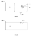
- FIG. 7 therein is shown a top view of the segment 600 of the first structure 106 , of FIG. 6 .
- the top view depicts the segment 600 of the first structure 106 having the compression via 108 .
- the compression via 108 is etched into the inner lead 602 of the first structure 106 that has been half etched.
- a sloped edge of the compression via 108 terminates at a smaller diameter 702 .
- FIG. 8 therein is shown a cross-sectional view of a leadframe lead 800 in an alternative embodiment of the first structure 106 , of FIG. 1 .
- the cross-sectional view of the leadframe lead 800 depicts a lead 802 having a blind via 804 .
- the blind via 804 would become a pressure chamber if an interference fit was made by a stud bump (not shown).
- the blind via 804 can have shapes, such as hexagons or triangles.
- FIG. 9 therein is shown a top view of a via construction on a leadframe lead 900 , in an alternative embodiment of the present invention.
- the top view depicts an alternative via 902 , such as a rectangular via, formed in the leadframe lead 900 .
- the alternative via 902 is formed by a process, such as punching, stamping or laser cutting.
- the alternative via 902 may have additional plating as required to meet the dimensional specifications.
- the rectangular shape of the alternative via 902 is for example and the shape may also be hexagonal, triangle or some other geometric shape.
- FIG. 10 therein is shown a top view of a via construction on a leadframe lead 1000 , in another alternative embodiment of the present invention.
- the top view depicts a longitudinally elongated via 1002 on the leadframe lead 1000 .
- the longitudinally elongated via 1002 is a preferred embodiment that allows for manufacturing tolerance in the position of a mating stud bump (not shown).
- the longitudinally elongated via 1002 is formed by a process, such as punching, stamping or laser cutting.
- the longitudinally elongated via 1002 may have additional plating as required to meet the dimensional specifications.
- FIG. 11 therein is shown a top view of a via construction on a leadframe lead 1100 , in yet another alternative embodiment of the present invention.
- the top view depicts a transverse elongated via 1102 on the leadframe lead 1100 .
- the transverse elongated via 1102 is a preferred embodiment that allows for manufacturing tolerance in the position of a mating stud bump (not shown).
- the transverse elongated via 1102 is formed by a process, such as punching, stamping or laser cutting.
- the transverse elongated via 1102 may have additional plating as required to meet the dimensional specifications.
- FIG. 12 therein is shown a more detailed cross-sectional view of the interface of the stud bump 104 to the first structure 106 , in an embodiment of the present invention.
- the more detailed cross-sectional view depicts the second structure 102 having the stud bump 104 attached thereon.
- the stud bump 104 is positioned within the compression via 108 of the first structure 106 , in preparation for the downward pressure that will form a mechanical bond between the compression via 108 and the stud bump 104 .
- FIG. 13 therein is shown a further detailed cross-sectional view of the interface of the stud bump 104 to the first structure 106 of FIG. 1 .
- the further detailed cross-sectional view of the interface depicts the second structure 102 having the stud bump 104 attached thereon.
- a metal deformation region 1302 is depicted at the surface of the first structure 106 where the diameter of the stud bump 104 exceeds the diameter of the compression via 108 .
- the design of the stud bump 104 relative to the opening of the compression via 108 determines a stand-off height 1304 .
- the height can be precisely placed based on the position where the diameter of the stud bump 104 exceeds the diameter of the compression via 108 . This aspect is important in the encapsulation phase of manufacture, as it allows molding compound to flow between the second structure 102 and the first structure 106 . In some applications the stand-off height 1304 may be set to zero.
- the use of the compression via 108 is for example, as the shape of the via may be different.
- a curved via may have sidewalls that are parabolic in curvature or a cylindrical via may have vertical side walls that have an outward flair at the top.
- Each of these shapes meet the criteria for an interference fit and will form the metal deformation region 1302 when the stud bump 104 is pressured into the opening of the selected via.
- FIG. 14 therein is shown a cross-section of an integrated circuit package system 1400 , in an alternative embodiment of the current invention.
- the cross-sectional view depicts an integrated circuit die 1402 having a stud bump 1404 , such as gold wire based stud bumps, pressure mounted in a via 1406 .
- the via 1406 is formed in a conductive layer 1408 , such as a copper layer, of a tape substrate 1410 .
- the tape substrate 1410 is formed of the conductive layer 1408 adhered to a support layer 1412 , such as polyimide.
- the via 1406 is formed in the conductive layer 1408 , system interconnects 1414 , such as solder balls are adhered to the bottom of the conductive layer 1408 .
- the top of the conductive layer 1408 and the integrated circuit die 1402 are encapsulated in a molding compound 1416 .
- FIG. 15 therein is shown a more detailed cross-sectional view of an interface 1500 of the stud bump 1404 to the tape substrate 1410 , in another alternative embodiment of the present invention.
- the more detailed cross-sectional view depicts a magnified section of the interface 1500 of the stud bump 1404 to the tape substrate 1410 .
- the support layer 1412 must be removed in a pressure support gap 1502 .
- a support beam (not shown) is inserted in the pressure support gap 1502 for the pressure bonding of the stud bump 1404 to the via 1406 in the conductive layer 1408 .
- the pressure bonding occurs when the stud bump 1404 is forced into the smaller opening in the via 1406 , creating a metal deformation region 1504 .
- the pressure bonding process is equivalent to thermo-compression bonding or thermo-sonic bonding, but requires less apparatus.
- the pressure support gap 1502 is filled in with a section of the support layer 1412 .
- FIG. 16 therein is shown a cross-sectional view of an integrated circuit package system 1600 , in yet another alternative embodiment of the present invention.
- the cross-sectional view depicts an integrated circuit die 1602 , having a stud bump 1604 , aligned and pressed into a via 1606 , such as a compression via, on a laminate substrate 1608 .
- the top of the laminate substrate 1608 and the integrated circuit die 1602 are encapsulated in a molding compound 1610 .
- System interconnects 1612 such as solder balls, are attached to the bottom of the laminate substrate 1608 for attachment to the next level system (not shown).
- FIG. 17 therein is shown a more detailed cross-sectional view of an interface 1700 between the stud bump 1604 and the laminate substrate 1608 , in an embodiment of the present invention.
- the more detailed cross-sectional view depicts a magnified section of the interface 1700 of the stud bump 1604 to the laminate substrate 1608 .
- the integrated circuit die 1602 has the stud bump 1604 attached to the active side.
- the stud bump 1604 is aligned with and pressed into the via 1606 that is formed in a signal layer 1702 of the laminate substrate 1608 .
- the pressure used in forcing a larger diameter of the stud bump 1604 into the smaller diameter of the via 1606 causes a mechanical bond in a metal deformation region 1704 .
- the position of the metal deformation region 1704 is determined by the slope of the stud bump 1604 and the slope of the via 1606 .
- the area of the metal deformation region 1704 is also determined by the contact surfaces that form the edges of the via 1606 .
- FIG. 18 therein is shown a cross-sectional view of a multi-chip package 1800 , in an alternative embodiment of the present invention.
- the cross-sectional view depicts a third structure 1802 , such as a laminate substrate, having a further compression via 1804 in a top signal layer 1806 and a bottom signal layer 1808 .
- the figure depicts only two signal layers for simplicity though it is understood that any number of signal layers is possible.
- a bottom first structure 1810 such as a tape substrate, is mounted to the bottom signal layer 1808 by pressure mounting of second stud bumps 1812 into the compression via 1804 forming a mechanical bond.
- the mechanical bond between the bottom signal layer 1808 and the bottom first structure 1810 also forms an electrical connection.
- a bottom second structure 1814 such as an integrated circuit die, is mounted on the bottom first structure 1810 .
- the bottom second structure 1814 has the stud bumps 1815 that are pressure mounted into the via 1406 on the bottom first structure 1810 forming a mechanical bond.
- the mechanical bond between the bottom second structure 1814 and the bottom first structure 1810 also forms an electrical connection.
- a top first structure 1816 such as the tape substrate, is mounted to the top signal layer 1806 by pressure mounting of the second stud bumps 1812 into the further compression via 1804 forming a mechanical bond.
- the mechanical bond between the top signal layer 1806 and the top first structure 1816 also forms an electrical connection.
- a top second structure 1818 such as the integrated circuit die, is mounted on the top first structure 1816 .
- the top second structure 1818 has the stud bumps 1815 that are pressure mounted into the via 1406 on the top first structure 1816 forming a mechanical bond.
- the mechanical bond between the top second structure 1818 and the top first structure 1816 also forms an electrical connection.
- a first wire bond integrated circuit die 1820 is attached to the bottom of the top first structure 1816 by a die attach material 1822 .
- the first wire bond integrated circuit die 1820 is electrically connected to the top signal layer 1806 by bond wires 1824 .
- the top of the third structure 1802 , the first wire bond integrated circuit die 1820 , the bottom of the top first structure 1816 and the bond wires 1824 are encapsulated by a molding compound 1826 .
- System interconnects 1828 are attached to the bottom signal layer 1808 , with a dielectric layer 1830 adhered around the system interconnects 1828 .
- a vent opening 1832 is optionally cut in the bottom first structure 1810 .
- FIG. 19 therein is shown a flow chart of an integrated circuit package system 1900 for manufacturing the integrated circuit package system 100 , in an embodiment of the present invention.
- the system 1900 includes providing a first structure in a block 1902 ; forming a compression via in the first structure in a block 1904 ; forming a stud bump on a second structure in a block 1906 ; and pressing the stud bump into the compression via forming a mechanical bond in a block 1908 .
- a method to manufacture an integrated circuit package system in an embodiment of the present invention is performed as follows:
- An aspect of the present invention is that, the mechanical bonding process enables assembly of an integrated circuit package without the use of lead (Pb) or solder flux. This process can be compatible with no-flow fluxing underfill (NFU) if necessary.
- Pb lead
- NFU no-flow fluxing underfill
- An aspect of the present invention is that the wafers don't require plated or printed bumps during fabrication. Bump studs are added later, using well known technology.
- Another aspect of the present invention is that by using a mechanical bonding process, no reflow is necessary. This allows the integrated circuit die to go through the assembly process without being exposed to excessive heat. This is an aspect that is important to heat sensitive die, such as MEMs.
- a die can be attached to a leadframe or substrate without subjecting the die to high reflow temperatures.
- Yet another important aspect of the present invention is that it valuably supports and services the historical trend of reducing costs, simplifying systems, and increasing performance.
- the integrated circuit package system method and apparatus of the present invention furnish important and heretofore unknown and unavailable solutions, capabilities, and functional aspects for integrated circuit package assembly without the use of high temperatures or polluting chemicals.
- the resulting processes and configurations are straightforward, cost-effective, uncomplicated, highly versatile and effective, can be implemented by adapting known technologies, and are thus readily suited for efficiently and economically manufacturing integrated circuit devices fully compatible with conventional manufacturing processes and technologies.
Abstract
Description
-
- 1. Providing a first structure. (
FIG. 1 ) - 2. Forming a compression via in the first structure by etching a diameter of the compression via. (
FIG. 1 ) - 3. Forming a stud bump on a second structure further comprises forming a conical shape. (
FIG. 1 ) and - 4. Forming a mechanical bond by pressing the stud bump into the compression via comprises forming a metal deformation region in the stud bump. (
FIG. 13 )
- 1. Providing a first structure. (
Claims (20)
Priority Applications (1)
| Application Number | Priority Date | Filing Date | Title |
|---|---|---|---|
| US11/276,727 US7790504B2 (en) | 2006-03-10 | 2006-03-10 | Integrated circuit package system |
Applications Claiming Priority (1)
| Application Number | Priority Date | Filing Date | Title |
|---|---|---|---|
| US11/276,727 US7790504B2 (en) | 2006-03-10 | 2006-03-10 | Integrated circuit package system |
Publications (2)
| Publication Number | Publication Date |
|---|---|
| US20070210425A1 US20070210425A1 (en) | 2007-09-13 |
| US7790504B2 true US7790504B2 (en) | 2010-09-07 |
Family
ID=38478104
Family Applications (1)
| Application Number | Title | Priority Date | Filing Date |
|---|---|---|---|
| US11/276,727 Active 2027-03-16 US7790504B2 (en) | 2006-03-10 | 2006-03-10 | Integrated circuit package system |
Country Status (1)
| Country | Link |
|---|---|
| US (1) | US7790504B2 (en) |
Cited By (8)
| Publication number | Priority date | Publication date | Assignee | Title |
|---|---|---|---|---|
| US20090212444A1 (en) * | 2008-02-21 | 2009-08-27 | Industrial Technology Research Institute | Semiconductor package and method of manufacturing the same |
| US20100244243A1 (en) * | 2009-03-24 | 2010-09-30 | Kabushiki Kaisha Toshiba | Semiconductor device |
| US20110042798A1 (en) * | 2009-08-21 | 2011-02-24 | Stats Chippac, Ltd. | Semiconductor Device and Method of Stacking Die on Leadframe Electrically Connected by Conductive Pillars |
| US20130264705A1 (en) * | 2010-04-21 | 2013-10-10 | Stats Chippac, Ltd. | Semiconductor Device and Method of Forming Bump on Substrate to Prevent ELK ILD Delamination During Reflow Process |
| US8866285B2 (en) | 2012-09-05 | 2014-10-21 | Taiwan Semiconductor Manufacturing Company, Ltd. | Fan-out package comprising bulk metal |
| US8922005B2 (en) * | 2012-04-11 | 2014-12-30 | Taiwan Semiconductor Manufacturing Company, Ltd. | Methods and apparatus for package on package devices with reversed stud bump through via interconnections |
| US9240380B2 (en) | 2009-08-21 | 2016-01-19 | Stats Chippac, Ltd. | Semiconductor device and method of forming interposer frame over semiconductor die to provide vertical interconnect |
| USRE48111E1 (en) | 2009-08-21 | 2020-07-21 | JCET Semiconductor (Shaoxing) Co. Ltd. | Semiconductor device and method of forming interposer frame over semiconductor die to provide vertical interconnect |
Families Citing this family (9)
| Publication number | Priority date | Publication date | Assignee | Title |
|---|---|---|---|---|
| US7859122B2 (en) | 2008-04-14 | 2010-12-28 | International Business Machines Corporation | Final via structures for bond pad-solder ball interconnections |
| US8049110B2 (en) * | 2008-10-01 | 2011-11-01 | Hewlett-Packard Development Company, L.P. | Microelectronic device |
| EP2261965A1 (en) * | 2009-06-12 | 2010-12-15 | Nxp B.V. | Crimp bump interconnection |
| EP2273545B1 (en) * | 2009-07-08 | 2016-08-31 | Imec | Method for insertion bonding and kit of parts for use in said method |
| AU2010332782B2 (en) * | 2009-12-18 | 2015-04-16 | Aerocrine Ab | Method for plugging a hole and a plugged hole |
| US8304900B2 (en) * | 2010-08-11 | 2012-11-06 | Stats Chippac Ltd. | Integrated circuit packaging system with stacked lead and method of manufacture thereof |
| US8476772B2 (en) | 2010-09-09 | 2013-07-02 | Stats Chippac, Ltd. | Semiconductor device and method of forming base substrate with recesses for capturing bumped semiconductor die |
| US8304277B2 (en) | 2010-09-09 | 2012-11-06 | Stats Chippac, Ltd. | Semiconductor device and method of forming base substrate with cavities formed through etch-resistant conductive layer for bump locking |
| US20130234344A1 (en) * | 2012-03-06 | 2013-09-12 | Triquint Semiconductor, Inc. | Flip-chip packaging techniques and configurations |
Citations (14)
| Publication number | Priority date | Publication date | Assignee | Title |
|---|---|---|---|---|
| US5742100A (en) * | 1995-03-27 | 1998-04-21 | Motorola, Inc. | Structure having flip-chip connected substrates |
| US20020060366A1 (en) * | 2000-11-20 | 2002-05-23 | Atsushi Kikuchi | Multilayer wiring substrate having differential signal wires and a general signal wire in different planes |
| US20020093108A1 (en) * | 2001-01-15 | 2002-07-18 | Grigorov Ilya L. | Flip chip packaged semiconductor device having double stud bumps and method of forming same |
| US20020149091A1 (en) * | 2001-04-16 | 2002-10-17 | Palmteer William James | Leadframe-based chip scale package |
| US6815252B2 (en) | 2000-03-10 | 2004-11-09 | Chippac, Inc. | Method of forming flip chip interconnection structure |
| US6828220B2 (en) | 2000-03-10 | 2004-12-07 | Chippac, Inc. | Flip chip-in-leadframe package and process |
| US20040262774A1 (en) * | 2003-06-27 | 2004-12-30 | In-Ku Kang | Multi-chip packages having a plurality of flip chips and methods of manufacturing the same |
| US20050095835A1 (en) * | 2003-09-26 | 2005-05-05 | Tessera, Inc. | Structure and method of making capped chips having vertical interconnects |
| US20050151273A1 (en) * | 2003-12-30 | 2005-07-14 | Arnold Richard W. | Semiconductor chip package |
| US20050167812A1 (en) * | 2003-01-15 | 2005-08-04 | Fujitsu Limited | Semiconductor device, three-dimensional semiconductor device, and method of manufacturing semiconductor device |
| US20060186514A1 (en) * | 2005-02-22 | 2006-08-24 | Stats Chippac Ltd. | Package stacking lead frame system |
| US20060220206A1 (en) * | 2005-03-29 | 2006-10-05 | Texas Instruments Incorporated | Vertically integrated system-in-a-package |
| US20070001296A1 (en) * | 2005-05-31 | 2007-01-04 | Stats Chippac Ltd. | Bump for overhang device |
| US20070148822A1 (en) * | 2005-12-23 | 2007-06-28 | Tessera, Inc. | Microelectronic packages and methods therefor |
-
2006
- 2006-03-10 US US11/276,727 patent/US7790504B2/en active Active
Patent Citations (14)
| Publication number | Priority date | Publication date | Assignee | Title |
|---|---|---|---|---|
| US5742100A (en) * | 1995-03-27 | 1998-04-21 | Motorola, Inc. | Structure having flip-chip connected substrates |
| US6815252B2 (en) | 2000-03-10 | 2004-11-09 | Chippac, Inc. | Method of forming flip chip interconnection structure |
| US6828220B2 (en) | 2000-03-10 | 2004-12-07 | Chippac, Inc. | Flip chip-in-leadframe package and process |
| US20020060366A1 (en) * | 2000-11-20 | 2002-05-23 | Atsushi Kikuchi | Multilayer wiring substrate having differential signal wires and a general signal wire in different planes |
| US20020093108A1 (en) * | 2001-01-15 | 2002-07-18 | Grigorov Ilya L. | Flip chip packaged semiconductor device having double stud bumps and method of forming same |
| US20020149091A1 (en) * | 2001-04-16 | 2002-10-17 | Palmteer William James | Leadframe-based chip scale package |
| US20050167812A1 (en) * | 2003-01-15 | 2005-08-04 | Fujitsu Limited | Semiconductor device, three-dimensional semiconductor device, and method of manufacturing semiconductor device |
| US20040262774A1 (en) * | 2003-06-27 | 2004-12-30 | In-Ku Kang | Multi-chip packages having a plurality of flip chips and methods of manufacturing the same |
| US20050095835A1 (en) * | 2003-09-26 | 2005-05-05 | Tessera, Inc. | Structure and method of making capped chips having vertical interconnects |
| US20050151273A1 (en) * | 2003-12-30 | 2005-07-14 | Arnold Richard W. | Semiconductor chip package |
| US20060186514A1 (en) * | 2005-02-22 | 2006-08-24 | Stats Chippac Ltd. | Package stacking lead frame system |
| US20060220206A1 (en) * | 2005-03-29 | 2006-10-05 | Texas Instruments Incorporated | Vertically integrated system-in-a-package |
| US20070001296A1 (en) * | 2005-05-31 | 2007-01-04 | Stats Chippac Ltd. | Bump for overhang device |
| US20070148822A1 (en) * | 2005-12-23 | 2007-06-28 | Tessera, Inc. | Microelectronic packages and methods therefor |
Cited By (14)
| Publication number | Priority date | Publication date | Assignee | Title |
|---|---|---|---|---|
| US20090212444A1 (en) * | 2008-02-21 | 2009-08-27 | Industrial Technology Research Institute | Semiconductor package and method of manufacturing the same |
| US20100244243A1 (en) * | 2009-03-24 | 2010-09-30 | Kabushiki Kaisha Toshiba | Semiconductor device |
| US9240380B2 (en) | 2009-08-21 | 2016-01-19 | Stats Chippac, Ltd. | Semiconductor device and method of forming interposer frame over semiconductor die to provide vertical interconnect |
| US8169058B2 (en) * | 2009-08-21 | 2012-05-01 | Stats Chippac, Ltd. | Semiconductor device and method of stacking die on leadframe electrically connected by conductive pillars |
| US9177901B2 (en) | 2009-08-21 | 2015-11-03 | Stats Chippac, Ltd. | Semiconductor device and method of stacking die on leadframe electrically connected by conductive pillars |
| US20110042798A1 (en) * | 2009-08-21 | 2011-02-24 | Stats Chippac, Ltd. | Semiconductor Device and Method of Stacking Die on Leadframe Electrically Connected by Conductive Pillars |
| US9893045B2 (en) | 2009-08-21 | 2018-02-13 | STATS ChipPAC Pte. Ltd. | Semiconductor device and method of forming interposer frame over semiconductor die to provide vertical interconnect |
| USRE48111E1 (en) | 2009-08-21 | 2020-07-21 | JCET Semiconductor (Shaoxing) Co. Ltd. | Semiconductor device and method of forming interposer frame over semiconductor die to provide vertical interconnect |
| USRE48408E1 (en) | 2009-08-21 | 2021-01-26 | Jcet Semiconductor (Shaoxing) Co., Ltd. | Semiconductor device and method of forming interposer frame over semiconductor die to provide vertical interconnect |
| US20130264705A1 (en) * | 2010-04-21 | 2013-10-10 | Stats Chippac, Ltd. | Semiconductor Device and Method of Forming Bump on Substrate to Prevent ELK ILD Delamination During Reflow Process |
| US8884339B2 (en) * | 2010-04-21 | 2014-11-11 | Stats Chippac, Ltd. | Semiconductor device with bump formed on substrate to prevent ELK ILD delamination during reflow process |
| US8922005B2 (en) * | 2012-04-11 | 2014-12-30 | Taiwan Semiconductor Manufacturing Company, Ltd. | Methods and apparatus for package on package devices with reversed stud bump through via interconnections |
| US9293449B2 (en) | 2012-04-11 | 2016-03-22 | Taiwan Semiconductor Manufacturing Company, Ltd. | Methods and apparatus for package on package devices with reversed stud bump through via interconnections |
| US8866285B2 (en) | 2012-09-05 | 2014-10-21 | Taiwan Semiconductor Manufacturing Company, Ltd. | Fan-out package comprising bulk metal |
Also Published As
| Publication number | Publication date |
|---|---|
| US20070210425A1 (en) | 2007-09-13 |
Similar Documents
| Publication | Publication Date | Title |
|---|---|---|
| US7790504B2 (en) | Integrated circuit package system | |
| US7993979B2 (en) | Leadless package system having external contacts | |
| US8643163B2 (en) | Integrated circuit package-on-package stacking system and method of manufacture thereof | |
| US6414381B1 (en) | Interposer for separating stacked semiconductor chips mounted on a multi-layer printed circuit board | |
| US8174105B2 (en) | Stacked semiconductor package having discrete components | |
| US6781240B2 (en) | Semiconductor package with semiconductor chips stacked therein and method of making the package | |
| US20070108583A1 (en) | Integrated circuit package-on-package stacking system | |
| US7732901B2 (en) | Integrated circuit package system with isloated leads | |
| US8420452B2 (en) | Fabrication method of leadframe-based semiconductor package | |
| KR101563911B1 (en) | Semiconductor package | |
| KR20080020069A (en) | Semiconductor package and method for fabricating the same | |
| US20100148172A1 (en) | Semiconductor device | |
| US8699232B2 (en) | Integrated circuit packaging system with interposer and method of manufacture thereof | |
| US20060284298A1 (en) | Chip stack package having same length bonding leads | |
| US7002246B2 (en) | Chip package structure with dual heat sinks | |
| KR101227078B1 (en) | Semiconductor package and method of forming the same | |
| KR102561718B1 (en) | Integrated circuit packaging system with interposer support structure mechanism and method of manufacture thereof | |
| US7498666B2 (en) | Stacked integrated circuit | |
| US7521781B2 (en) | Integrated circuit package system with mold clamp line critical area having widened conductive traces | |
| US8159063B2 (en) | Substrate and package with micro BGA configuration | |
| US7656021B2 (en) | Integrated circuit package system with pedestal structure | |
| KR20090036948A (en) | Bga package and method for fabricating of the same | |
| US20240105569A1 (en) | Integrated package and method for making the same | |
| KR20070016399A (en) | chip on glass package using glass substrate | |
| KR101096440B1 (en) | Dual Die Package |
Legal Events
| Date | Code | Title | Description |
|---|---|---|---|
| AS | Assignment |
Owner name: STATS CHIPPAC LTD., SINGAPORE Free format text: ASSIGNMENT OF ASSIGNORS INTEREST;ASSIGNORS:RAMAKRISHNA, KAMBHAMPATI;HAN, BYUNG JOON;CHOW, SENG GUAN;REEL/FRAME:017308/0804;SIGNING DATES FROM 20060228 TO 20060301 Owner name: STATS CHIPPAC LTD., SINGAPORE Free format text: ASSIGNMENT OF ASSIGNORS INTEREST;ASSIGNORS:RAMAKRISHNA, KAMBHAMPATI;HAN, BYUNG JOON;CHOW, SENG GUAN;SIGNING DATES FROM 20060228 TO 20060301;REEL/FRAME:017308/0804 |
|
| STCF | Information on status: patent grant |
Free format text: PATENTED CASE |
|
| FPAY | Fee payment |
Year of fee payment: 4 |
|
| AS | Assignment |
Owner name: CITICORP INTERNATIONAL LIMITED, AS COMMON SECURITY AGENT, HONG KONG Free format text: SECURITY INTEREST;ASSIGNORS:STATS CHIPPAC, INC.;STATS CHIPPAC LTD.;REEL/FRAME:036288/0748 Effective date: 20150806 Owner name: CITICORP INTERNATIONAL LIMITED, AS COMMON SECURITY Free format text: SECURITY INTEREST;ASSIGNORS:STATS CHIPPAC, INC.;STATS CHIPPAC LTD.;REEL/FRAME:036288/0748 Effective date: 20150806 |
|
| AS | Assignment |
Owner name: STATS CHIPPAC PTE. LTE., SINGAPORE Free format text: CHANGE OF NAME;ASSIGNOR:STATS CHIPPAC LTD.;REEL/FRAME:038378/0309 Effective date: 20160329 |
|
| MAFP | Maintenance fee payment |
Free format text: PAYMENT OF MAINTENANCE FEE, 8TH YEAR, LARGE ENTITY (ORIGINAL EVENT CODE: M1552) Year of fee payment: 8 |
|
| AS | Assignment |
Owner name: STATS CHIPPAC, INC., CALIFORNIA Free format text: RELEASE BY SECURED PARTY;ASSIGNOR:CITICORP INTERNATIONAL LIMITED, AS COMMON SECURITY AGENT;REEL/FRAME:052924/0007 Effective date: 20190503 Owner name: STATS CHIPPAC PTE. LTD. FORMERLY KNOWN AS STATS CHIPPAC LTD., SINGAPORE Free format text: RELEASE BY SECURED PARTY;ASSIGNOR:CITICORP INTERNATIONAL LIMITED, AS COMMON SECURITY AGENT;REEL/FRAME:052924/0007 Effective date: 20190503 |
|
| MAFP | Maintenance fee payment |
Free format text: PAYMENT OF MAINTENANCE FEE, 12TH YEAR, LARGE ENTITY (ORIGINAL EVENT CODE: M1553); ENTITY STATUS OF PATENT OWNER: LARGE ENTITY Year of fee payment: 12 |
|
| AS | Assignment |
Owner name: STATS CHIPPAC PTE. LTD., SINGAPORE Free format text: CORRECTIVE ASSIGNMENT TO CORRECT THE THE ASSIGNEE'S NAME PREVIOUSLY RECORDED AT REEL: 038378 FRAME: 0309. ASSIGNOR(S) HEREBY CONFIRMS THE ASSIGNMENT;ASSIGNOR:STATS CHIPPAC LTD.;REEL/FRAME:065236/0767 Effective date: 20160329 |