US7807532B2 - Method and structure for self aligned formation of a gate polysilicon layer - Google Patents
Method and structure for self aligned formation of a gate polysilicon layer Download PDFInfo
- Publication number
- US7807532B2 US7807532B2 US11/623,048 US62304807A US7807532B2 US 7807532 B2 US7807532 B2 US 7807532B2 US 62304807 A US62304807 A US 62304807A US 7807532 B2 US7807532 B2 US 7807532B2
- Authority
- US
- United States
- Prior art keywords
- silicon nitride
- polishing process
- nitride layer
- isolation structure
- oxide
- Prior art date
- Legal status (The legal status is an assumption and is not a legal conclusion. Google has not performed a legal analysis and makes no representation as to the accuracy of the status listed.)
- Active, expires
Links
- 238000000034 method Methods 0.000 title claims abstract description 113
- 229910021420 polycrystalline silicon Inorganic materials 0.000 title claims abstract description 47
- 229920005591 polysilicon Polymers 0.000 title claims abstract description 47
- 230000015572 biosynthetic process Effects 0.000 title claims description 9
- 239000000463 material Substances 0.000 claims abstract description 47
- 238000002955 isolation Methods 0.000 claims abstract description 41
- 229910052581 Si3N4 Inorganic materials 0.000 claims abstract description 40
- HQVNEWCFYHHQES-UHFFFAOYSA-N silicon nitride Chemical compound N12[Si]34N5[Si]62N3[Si]51N64 HQVNEWCFYHHQES-UHFFFAOYSA-N 0.000 claims abstract description 39
- 239000004065 semiconductor Substances 0.000 claims abstract description 31
- 239000000758 substrate Substances 0.000 claims abstract description 26
- 239000000126 substance Substances 0.000 claims description 26
- 238000007517 polishing process Methods 0.000 claims description 25
- 238000004519 manufacturing process Methods 0.000 claims description 18
- 238000000151 deposition Methods 0.000 claims description 5
- 238000005137 deposition process Methods 0.000 claims description 5
- 238000012545 processing Methods 0.000 abstract description 5
- 238000007796 conventional method Methods 0.000 description 13
- XUIMIQQOPSSXEZ-UHFFFAOYSA-N Silicon Chemical compound [Si] XUIMIQQOPSSXEZ-UHFFFAOYSA-N 0.000 description 11
- 229910052710 silicon Inorganic materials 0.000 description 11
- 239000010703 silicon Substances 0.000 description 11
- VYPSYNLAJGMNEJ-UHFFFAOYSA-N Silicium dioxide Chemical compound O=[Si]=O VYPSYNLAJGMNEJ-UHFFFAOYSA-N 0.000 description 10
- 230000007547 defect Effects 0.000 description 10
- 229910052814 silicon oxide Inorganic materials 0.000 description 10
- 238000012986 modification Methods 0.000 description 9
- 230000004048 modification Effects 0.000 description 9
- 239000002243 precursor Substances 0.000 description 8
- 238000010586 diagram Methods 0.000 description 7
- 238000005530 etching Methods 0.000 description 7
- 235000012431 wafers Nutrition 0.000 description 7
- 230000003628 erosive effect Effects 0.000 description 6
- 238000000623 plasma-assisted chemical vapour deposition Methods 0.000 description 6
- 238000005498 polishing Methods 0.000 description 6
- MROCJMGDEKINLD-UHFFFAOYSA-N dichlorosilane Chemical compound Cl[SiH2]Cl MROCJMGDEKINLD-UHFFFAOYSA-N 0.000 description 5
- 238000002474 experimental method Methods 0.000 description 5
- 238000001020 plasma etching Methods 0.000 description 5
- KRHYYFGTRYWZRS-UHFFFAOYSA-N Fluorane Chemical compound F KRHYYFGTRYWZRS-UHFFFAOYSA-N 0.000 description 4
- QVGXLLKOCUKJST-UHFFFAOYSA-N atomic oxygen Chemical compound [O] QVGXLLKOCUKJST-UHFFFAOYSA-N 0.000 description 4
- 238000004518 low pressure chemical vapour deposition Methods 0.000 description 4
- 239000001301 oxygen Substances 0.000 description 4
- 229910052760 oxygen Inorganic materials 0.000 description 4
- BLRPTPMANUNPDV-UHFFFAOYSA-N Silane Chemical compound [SiH4] BLRPTPMANUNPDV-UHFFFAOYSA-N 0.000 description 3
- BOTDANWDWHJENH-UHFFFAOYSA-N Tetraethyl orthosilicate Chemical compound CCO[Si](OCC)(OCC)OCC BOTDANWDWHJENH-UHFFFAOYSA-N 0.000 description 3
- 238000005229 chemical vapour deposition Methods 0.000 description 3
- 239000007943 implant Substances 0.000 description 3
- 239000012212 insulator Substances 0.000 description 3
- 238000001459 lithography Methods 0.000 description 3
- 238000001878 scanning electron micrograph Methods 0.000 description 3
- 229910000077 silane Inorganic materials 0.000 description 3
- XKRFYHLGVUSROY-UHFFFAOYSA-N Argon Chemical compound [Ar] XKRFYHLGVUSROY-UHFFFAOYSA-N 0.000 description 2
- NBIIXXVUZAFLBC-UHFFFAOYSA-N Phosphoric acid Chemical compound OP(O)(O)=O NBIIXXVUZAFLBC-UHFFFAOYSA-N 0.000 description 2
- 238000005516 engineering process Methods 0.000 description 2
- 238000002513 implantation Methods 0.000 description 2
- 150000004767 nitrides Chemical class 0.000 description 2
- 230000002093 peripheral effect Effects 0.000 description 2
- 125000006850 spacer group Chemical group 0.000 description 2
- ZOXJGFHDIHLPTG-UHFFFAOYSA-N Boron Chemical compound [B] ZOXJGFHDIHLPTG-UHFFFAOYSA-N 0.000 description 1
- 229910000147 aluminium phosphate Inorganic materials 0.000 description 1
- 229910052786 argon Inorganic materials 0.000 description 1
- 229910052796 boron Inorganic materials 0.000 description 1
- 230000032798 delamination Effects 0.000 description 1
- 239000002019 doping agent Substances 0.000 description 1
- -1 e.g. Substances 0.000 description 1
- 238000007667 floating Methods 0.000 description 1
- 150000002500 ions Chemical class 0.000 description 1
- 230000000873 masking effect Effects 0.000 description 1
- 238000000059 patterning Methods 0.000 description 1
- 229920002120 photoresistant polymer Polymers 0.000 description 1
- 230000003068 static effect Effects 0.000 description 1
Images


Classifications
-
- H—ELECTRICITY
- H10—SEMICONDUCTOR DEVICES; ELECTRIC SOLID-STATE DEVICES NOT OTHERWISE PROVIDED FOR
- H10B—ELECTRONIC MEMORY DEVICES
- H10B69/00—Erasable-and-programmable ROM [EPROM] devices not provided for in groups H10B41/00 - H10B63/00, e.g. ultraviolet erasable-and-programmable ROM [UVEPROM] devices
-
- H—ELECTRICITY
- H01—ELECTRIC ELEMENTS
- H01L—SEMICONDUCTOR DEVICES NOT COVERED BY CLASS H10
- H01L21/00—Processes or apparatus adapted for the manufacture or treatment of semiconductor or solid state devices or of parts thereof
- H01L21/70—Manufacture or treatment of devices consisting of a plurality of solid state components formed in or on a common substrate or of parts thereof; Manufacture of integrated circuit devices or of parts thereof
- H01L21/71—Manufacture of specific parts of devices defined in group H01L21/70
- H01L21/76—Making of isolation regions between components
- H01L21/762—Dielectric regions, e.g. EPIC dielectric isolation, LOCOS; Trench refilling techniques, SOI technology, use of channel stoppers
- H01L21/76224—Dielectric regions, e.g. EPIC dielectric isolation, LOCOS; Trench refilling techniques, SOI technology, use of channel stoppers using trench refilling with dielectric materials
-
- H—ELECTRICITY
- H01—ELECTRIC ELEMENTS
- H01L—SEMICONDUCTOR DEVICES NOT COVERED BY CLASS H10
- H01L29/00—Semiconductor devices adapted for rectifying, amplifying, oscillating or switching, or capacitors or resistors with at least one potential-jump barrier or surface barrier, e.g. PN junction depletion layer or carrier concentration layer; Details of semiconductor bodies or of electrodes thereof ; Multistep manufacturing processes therefor
- H01L29/66—Types of semiconductor device ; Multistep manufacturing processes therefor
- H01L29/66007—Multistep manufacturing processes
- H01L29/66075—Multistep manufacturing processes of devices having semiconductor bodies comprising group 14 or group 13/15 materials
- H01L29/66227—Multistep manufacturing processes of devices having semiconductor bodies comprising group 14 or group 13/15 materials the devices being controllable only by the electric current supplied or the electric potential applied, to an electrode which does not carry the current to be rectified, amplified or switched, e.g. three-terminal devices
- H01L29/66409—Unipolar field-effect transistors
- H01L29/66477—Unipolar field-effect transistors with an insulated gate, i.e. MISFET
- H01L29/66545—Unipolar field-effect transistors with an insulated gate, i.e. MISFET using a dummy, i.e. replacement gate in a process wherein at least a part of the final gate is self aligned to the dummy gate
-
- H—ELECTRICITY
- H10—SEMICONDUCTOR DEVICES; ELECTRIC SOLID-STATE DEVICES NOT OTHERWISE PROVIDED FOR
- H10B—ELECTRONIC MEMORY DEVICES
- H10B41/00—Electrically erasable-and-programmable ROM [EEPROM] devices comprising floating gates
- H10B41/30—Electrically erasable-and-programmable ROM [EEPROM] devices comprising floating gates characterised by the memory core region
-
- H—ELECTRICITY
- H01—ELECTRIC ELEMENTS
- H01L—SEMICONDUCTOR DEVICES NOT COVERED BY CLASS H10
- H01L21/00—Processes or apparatus adapted for the manufacture or treatment of semiconductor or solid state devices or of parts thereof
- H01L21/02—Manufacture or treatment of semiconductor devices or of parts thereof
- H01L21/04—Manufacture or treatment of semiconductor devices or of parts thereof the devices having at least one potential-jump barrier or surface barrier, e.g. PN junction, depletion layer or carrier concentration layer
- H01L21/18—Manufacture or treatment of semiconductor devices or of parts thereof the devices having at least one potential-jump barrier or surface barrier, e.g. PN junction, depletion layer or carrier concentration layer the devices having semiconductor bodies comprising elements of Group IV of the Periodic System or AIIIBV compounds with or without impurities, e.g. doping materials
- H01L21/26—Bombardment with radiation
- H01L21/263—Bombardment with radiation with high-energy radiation
- H01L21/265—Bombardment with radiation with high-energy radiation producing ion implantation
- H01L21/26506—Bombardment with radiation with high-energy radiation producing ion implantation in group IV semiconductors
- H01L21/26513—Bombardment with radiation with high-energy radiation producing ion implantation in group IV semiconductors of electrically active species
- H01L21/2652—Through-implantation
-
- H—ELECTRICITY
- H01—ELECTRIC ELEMENTS
- H01L—SEMICONDUCTOR DEVICES NOT COVERED BY CLASS H10
- H01L29/00—Semiconductor devices adapted for rectifying, amplifying, oscillating or switching, or capacitors or resistors with at least one potential-jump barrier or surface barrier, e.g. PN junction depletion layer or carrier concentration layer; Details of semiconductor bodies or of electrodes thereof ; Multistep manufacturing processes therefor
- H01L29/66—Types of semiconductor device ; Multistep manufacturing processes therefor
- H01L29/66007—Multistep manufacturing processes
- H01L29/66075—Multistep manufacturing processes of devices having semiconductor bodies comprising group 14 or group 13/15 materials
- H01L29/66227—Multistep manufacturing processes of devices having semiconductor bodies comprising group 14 or group 13/15 materials the devices being controllable only by the electric current supplied or the electric potential applied, to an electrode which does not carry the current to be rectified, amplified or switched, e.g. three-terminal devices
- H01L29/66409—Unipolar field-effect transistors
- H01L29/66477—Unipolar field-effect transistors with an insulated gate, i.e. MISFET
- H01L29/66825—Unipolar field-effect transistors with an insulated gate, i.e. MISFET with a floating gate
Definitions
- the present invention is directed to integrated circuits and their processing for the manufacture of semiconductor devices. More particularly, the invention provides a method and structures for manufacturing gate structures for NOR flash memory integrated circuit devices, commonly called Flash devices. But it would be recognized that the invention has a much broader range of applicability.
- Integrated circuits have evolved from a handful of interconnected devices fabricated on a single chip of silicon to millions of devices.
- Conventional integrated circuits provide performance and complexity far beyond what was originally imagined.
- the size of the smallest device feature also known as the device “geometry”, has become smaller with each generation of integrated circuits.
- the invention provides a method and structures for manufacturing gate structures for NOR flash memory integrated circuit devices, commonly known as Flash devices. But it would be recognized that the invention has a much broader range of applicability. For example, the invention can be applied to a variety of devices such as dynamic random access memory devices, static random access memory devices, application specific integrated circuit devices, microprocessors, microcontrollers, and others.
- the invention provides a method for processing semiconductor devices.
- the method includes providing a semiconductor substrate, which comprises a surface region.
- the semiconductor substrate can be silicon, silicon on insulator, epitaxial silicon or the like.
- the method includes forming a pad oxide layer overlying the surface region.
- the pad oxide layer has a pad oxide surface region.
- the method includes forming a silicon nitride layer overlying the pad oxide layer.
- the method includes forming a trench region.
- the trench region extends through an entirety of a portion of the silicon nitride layer and extends into a depth of the semiconductor substrate.
- the method also includes filling the trench region with an oxide material using a plasma deposition process.
- the oxide material extends from a bottom portion of the trench region to a vicinity of an upper surface region of the silicon nitride layer.
- the method includes planarizing the oxide material and exposing a surface of the silicon nitride layer.
- the method includes selectively removing the silicon nitride layer to cause formation of an isolation structure.
- the isolation structure extends from the bottom portion of the trench region to a height above a the pad oxide surface region.
- the method includes stripping the pad oxide layer and forming a tunnel oxide structure overlying a portion of the semiconductor substrate.
- the method also includes depositing a conformal layer of polysilicon material overlying the isolation structure and the tunnel oxide structure.
- the method includes planarizing the polysilicon material to expose a top portion of the isolation structure and form a first electrode structure and a second electrode structure separated by a portion of the isolation structure
- the present technique provides an easy to use process that relies upon conventional technology.
- the method provides means to reduce process steps and higher device yields in dies per wafer.
- the method provides a process that is compatible with conventional equipment and processes.
- the method can be applied to a variety of applications such as memory, application specific integrated circuit, microprocessor, and others.
- the invention provides a method to fabricate gate structures for integrated circuit devices. Depending on the embodiment, one or more of these benefits may be achieved.
- FIG. 1( a ) through 1 ( p ) are simplified diagrams illustrating a conventional method of manufacturing an integrated circuit.
- FIG. 2( a ) through 2 ( k ) are simplified diagrams illustrating a method of manufacturing an integrated circuit according to an embodiment of the present invention.
- FIG. 3 is a simplified top view diagram of cell region according to an embodiment of the present invention.
- FIG. 4 is a simplified diagram of a gate structure according to a conventional method of manufacturing an integrated circuit.
- FIG. 5 is a scanning electron micrograph of a device structure according to a conventional method of manufacturing an integrated circuit.
- FIG. 6 is a profiler scan of a device structure according to a conventional method of manufacturing an integrated circuit.
- FIG. 7 is a profiler scan of a device structure using a preferred method according to an embodiment of the present embodiment.
- FIG. 8 shows a scanning electron micrograph of a gate structure according to a conventional method of manufacturing an integrated circuit.
- the invention provides a method for fabricating gate structures for memory devices. But it would be recognized that the invention has a much broader range of applicability. For example, the invention can be applied to application specific integrated circuit devices, logic devices, and others.
- FIG. 1( a ) to 1 ( q ) are simplified diagrams illustrating a conventional method of fabricating gate structures for integrated circuit devices.
- the conventional method includes providing a semiconductor substrate 100 having a surface.
- a dielectric stack is formed overlying the semiconductor substrate.
- the dielectric stack often comprises of silicon oxide 102 , silicon nitride 104 , and silicon oxynitride 106 .
- the dielectric stack and a portion of the semiconductor substrate is subjected to a first masking and etch process to form a trench region 108 as shown in FIG. 1( b ).
- An oxide material 110 is deposited overlying the dielectric stack and filling the trench region 108 as shown in FIG. 1( c ).
- the oxide material is usually silicon oxide formed using a high density plasma process.
- the dielectric stack and the oxide material is planarized using a chemical mechanical polishing process exposing a top surface of the isolation region.
- the top surface of the isolation region is even with silicon nitride layer 104 .
- a first selective etching process removes silicon nitride and shown in FIG. 1( f ), a second etching process removes silicon oxide, forming an isolation region 114 .
- the isolation region has a height of about 250 ⁇ from the surface of the semiconductor substrate.
- An implant process provides source/drain regions and a channel regions in the semiconductor substrate as shown in FIG. 1( g ).
- the conventional method includes forming a tunnel oxide 116 overlying the semiconductor substrate.
- a polysilicon material 118 is deposited overlying the tunnel oxide and isolation region 114 as shown in FIG. 1( i ).
- a silicon nitride layer 120 is formed overlying polysilicon material 118 as shown in FIG. 1( j ).
- a photoresist material is formed overlying the silicon nitride layer 120 as shown in FIG. 1( k ).
- a second pattern and selective etch process form an opening 122 in the silicon nitride layer as shown in FIG. 1( l ).
- the opening 122 is aligned to form above the isolation structure 114 .
- a third silicon nitride layer 124 is formed conformally overlying the second silicon nitride layer including the opening 122 .
- the third silicon nitride layer is subjected to a pattern and etch process to form spacer structure 126 as shown in FIG.
- the polysilicon material 116 is etched using the third silicon nitride layer and the second silicon nitride layer as a hard mask to form gate structures as shown in FIG. 1( o ).
- a selective etching process removes the spacer structure and the second silicon nitride layer forming gate structures 130 separated by the isolation structure 114 as shown in FIG. 1( p ).
- a semiconductor substrate e.g., silicon wafer, silicon on insulator, or epitaxial silicon.
- the above sequence of steps provides a method for fabricating gate structure for integrated circuit device according to an embodiment of the present invention. As shown, the method uses a combination of steps including a way of forming a gate structure using a self-align gate formation technique. Other alternatives can also be provided where steps are added, one or more steps are removed or one or more steps are provide in a different sequence without departing from the scope of the claims herein. Further details of the present invention can be found throughout the present specification and more particularly below.
- FIG. 2( a )- 2 ( k ) are a simplified diagrams illustrating a method for fabricating a gate structure according to an embodiment of the present invention.
- the diagrams are merely examples which should not unduly limit the scope of the claims herein.
- the present invention provides a method for forming a gate structure for integrated circuit devices.
- the method includes providing a semiconductor substrate 200 having a surface.
- the semiconductor substrate can be silicon wafer, silicon on insulator, epitaxial silicon, or the like.
- the method includes forming a pad oxide 202 overlying the semiconductor substrate.
- the pad oxide can be a thermal oxide.
- the pad oxide can also be deposited using a chemical vapor deposition process or other suitable processes.
- a silicon nitride layer 204 is formed overlying pad oxide layer 202 .
- the silicon nitride layer can be formed using a chemical vapor deposition process using dichlorosilane and NH 3 as precursors. Other suitable process such as a plasma enhanced chemical vapor deposition may also be used depending on the application.
- a trench region 206 is formed using a pattern and etch process.
- a reactive ion etching process can be used.
- Other etching techniques such as wet etch may also be used depending on the application.
- the trench region 206 extends through an entire thickness of silicon nitride layer and to a depth 208 in the semiconductor substrate.
- the depth 208 ranges from 2000 ⁇ to 4500 ⁇ in certain embodiments.
- the method includes depositing an oxide material 210 overlying the silicon nitride layer and filling the trench region 206 as shown in FIG. 2( c ).
- the oxide material comprises of silicon oxide deposited using a high density plasma (HDP) process using precursors such as silane and oxygen in an argon ambient. Other suitable precursors may also be used.
- HDP high density plasma
- Other suitable deposition process such as low pressure chemical vapor deposition, (LPCVD), plasma enhanced chemical vapor deposition (PECVD) may also be used.
- the method includes planarizing the oxide material, exposing a surface of the silicon nitride layer and a top surface of the oxide material in the trench region 211 using a planarizing process.
- the top surface of the oxide material is substantially level and even with the patterned nitride layer.
- a chemical mechanical polishing process can be used for the planarizing process.
- the chemical mechanical polishing process uses a high selectivity chemical mechanical polishing process and the nitride layer as a stop (e.g., a polish stop).
- Other suitable planarizing process may also be used. These other techniques can include etch back, reflow, and/or other combinations.
- the silicon nitride layer remains at a thickness ranges from 1500 to 2000 ⁇ in cell region. Of course, there can be other variations, modifications, and alternatives.
- FIG. 2( e ) illustrates the formation of an isolation structure 213 according to an embodiment of the present invention.
- a selective silicon nitride etch process removes the silicon nitride layer
- an oxide strip process removes the pad oxide layer and a portion of the oxide material, exposing the oxide material to a height of 212 above the surface of the semiconductor substrate as shown in FIG. 2( e ).
- a wet etch using phosphoric acid species is used for the selective silicon nitride etch process.
- Other selective silicon nitride etch process such as reactive ion etching (RIE) may also be used.
- the oxide strip process uses an aqueous hydrofluoric acid species.
- Other suitable oxide strip process such as reactive ion etching (RIE) may also be used.
- the height 212 ranges from 1000 to 2000 ⁇ in certain embodiment. Of course, one of ordinary skill in the art would recognize many other variations, modifications, and alternatives.
- the method includes forming source/drain regions 216 and a channel region 218 using an implantation process.
- the implantation process includes using boron as dopants at a dose of 1.4 ⁇ 10 13 to 1.6 ⁇ 10 13 atoms per cm 2 and at an energy of 75 keV to 85 keV. Other implant parameters may also be used depending on the application.
- the method includes forming a tunnel oxide 220 overlying the semiconductor substrate as shown in FIG. 2( g ).
- the tunnel oxide can be formed using a chemical vapor deposition process using tetraethyl orthosilicate as precursor. Other suitable silicon oxide deposition process may also be used. These other processes include low pressure chemical vapor deposition process using dichlorosilane (DCS) and oxygen as precursors, plasma enhanced chemical vapor deposition (PECVD), among others.
- the tunnel oxide can be formed using a oxide growth process.
- the method includes depositing a conformal layer of polysilicon material 222 overlying the isolation structure and the tunnel oxide s shown in FIG. 2( h ).
- the polysilicon material is formed using a chemical vapor depositing process and silane as precursor in a specific embodiment.
- a cap oxide layer 224 is formed overlying the conformal polysilicon material.
- the cap oxide layer is formed using a low pressure chemical vapor deposition process and dichlorosilane (DCS) and oxygen as precursors. Other precursors such as tetraethyl orthosilicate (TEOS) or silane and oxygen may also be used. Other deposition processes such as plasma enhanced chemical vapor deposition may also be used.
- the cap oxide layer protects the polysilicon material during chemical mechanical polishing by preventing delamination of the polysilicon material.
- the cap oxide layer also protects large polysilicon area and reduces polysilicon dishing.
- the method includes planarizing the polysilicon material and exposing a portion of the isolation structure using a planarizing process according to an embodiment of the present invention.
- the planarizing process includes a multi-step chemical mechanical polishing process in a preferred embodiment.
- the multi-step chemical mechanical polishing process includes a first chemical mechanical polishing step, a second chemical mechanical polishing step, and a third chemical mechanical polishing step.
- the first chemical mechanical polishing step planarizes the conformal polysilicon material and a leaves a thickness 226 on top of the isolating structure 213 as shown in FIG. 2( i ). Thickness 226 ranges from 200 ⁇ to 400 ⁇ in certain embodiments.
- the first chemical mechanical polishing step includes a low selectivity chemical mechanical polishing process using a hard pad operating at a medium down force, at a medium table speed, and at a low head rotating speed.
- the medium down force is between 2 pounds per square inch and 4 pounds per square inch
- the medium table speed is less than 70 revolutions per minute
- the low head rotating speed is less than 70 revolutions per minute.
- the second chemical mechanical polishing process uses a high selectivity chemical mechanical polishing process to expose a portion of the isolation structure.
- the high selectivity chemical mechanical polishing process uses the oxide material in the trench region as a stop.
- the high selectivity chemical mechanical polishing process includes using a low down force of less than 2.0 pounds per square inch, a low table speed of less than 35 revolutions per minute, and a low head rotary speed of less than 35 revolutions per minute in a specific embodiment.
- the third chemical mechanical polishing process uses an over polishing process to remove all the polysilicon material on the isolation structure as shown in FIG. 2( j ). As shown, a top surface of the oxide material is exposed and substantially even with the polysilicon material.
- the over polishing process includes using a hard pad, a low down force of less than 2.0 pounds per inch, a low table speed of less than 35 revolutions per minute, and a low head rotary speed of less than 35 revolutions per minute in a specific embodiment.
- a hard pad a low down force of less than 2.0 pounds per inch
- a low table speed of less than 35 revolutions per minute and a low head rotary speed of less than 35 revolutions per minute
- the multi-step polishing process eliminates polysilicon line dishing in cell area, improves within wafer polysilicon thickness uniformity and improves polysilicon thickness control.
- the multi-step polishing process eliminates polysilicon line dishing in cell area, improves within wafer polysilicon thickness uniformity and improves polysilicon thickness control.
- the method includes a selective oxide etching process to remove a portion of the isolation material, forming gate structures 228 and 230 .
- the gate structures are separated by the isolation structure as shown in FIG. 2( k ).
- the selective etching process includes a wet etch using a buffered hydrofluoric acid species.
- Other suitable selective oxide etching process such as a reactive ion etch may also be used depending on the application.
- the gate structures are floating gate structures for a Flash memory device.
- the method also includes forming a plurality of dummy structures in a peripheral area 301 as shown in FIG. 3 .
- the peripheral area surrounds memory cell region 302 .
- the dummy structures reduces erosion of oxide material in the isolation structure during multi-step chemical mechanical polishing process.
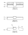
- FIG. 4 illustrates polysilicon line dishing defect in cell region when a conventional CMP process is used in polysilicon gate formation.
- a semiconductor substrate 400 is shown.
- Polysilicon dishing 401 can range from 200 ⁇ to 300 ⁇ in polysilicon gate structure 402 separated by an isolation structure 403 .
- Polysilicon dishing defect is even more severe in non-cell region or large polysilicon area 501 as shown in scanning electron microscope picture in FIG. 5 .
- Polysilicon dishing in large polysilicon area with area size of 100 ⁇ 100 ⁇ m 2 can be greater than 1500 ⁇ .
- FIG. 6 illustrates erosion 600 of the isolation structure.
- the defect shows a hump 602 of about 200-400 ⁇ in height and an erosion 604 of about 400-700 ⁇ in the isolation structure when a conventional polysilicon CMP is used.
- FIG. 7 shows profiler scans of an isolation structure using the preferred method according to the present invention.
- erosion in isolation region was reduced to about 80 ⁇ or less after multi-step polysilicon CMP process in preferred embodiment.
- FIG. 8 Scanning electron micrograph of a polysilicon gate structure fabricated using a conventional method is shown in FIG. 8 .
- a misalignment of photomask or hard mask in polysilicon gate formation resulted in misalignment in polysilicon etch 801 and device defect.
- such defects were eliminated as no photomask is needed for forming self-aligned polysilicon gate according to embodiments of present invention.
Abstract
Description
Claims (6)
Applications Claiming Priority (3)
| Application Number | Priority Date | Filing Date | Title |
|---|---|---|---|
| CNB2006100256460A CN100539080C (en) | 2006-04-12 | 2006-04-12 | Form the method for multi-crystal silicon floating bar structure by autoregistration |
| CN200610025646 | 2006-04-12 | ||
| CN200610025646.0 | 2006-04-12 |
Publications (2)
| Publication Number | Publication Date |
|---|---|
| US20070243685A1 US20070243685A1 (en) | 2007-10-18 |
| US7807532B2 true US7807532B2 (en) | 2010-10-05 |
Family
ID=38605319
Family Applications (1)
| Application Number | Title | Priority Date | Filing Date |
|---|---|---|---|
| US11/623,048 Active 2028-07-20 US7807532B2 (en) | 2006-04-12 | 2007-01-12 | Method and structure for self aligned formation of a gate polysilicon layer |
Country Status (2)
| Country | Link |
|---|---|
| US (1) | US7807532B2 (en) |
| CN (1) | CN100539080C (en) |
Families Citing this family (139)
| Publication number | Priority date | Publication date | Assignee | Title |
|---|---|---|---|---|
| US9324576B2 (en) | 2010-05-27 | 2016-04-26 | Applied Materials, Inc. | Selective etch for silicon films |
| US10283321B2 (en) | 2011-01-18 | 2019-05-07 | Applied Materials, Inc. | Semiconductor processing system and methods using capacitively coupled plasma |
| US9064815B2 (en) | 2011-03-14 | 2015-06-23 | Applied Materials, Inc. | Methods for etch of metal and metal-oxide films |
| US8999856B2 (en) | 2011-03-14 | 2015-04-07 | Applied Materials, Inc. | Methods for etch of sin films |
| US8771536B2 (en) | 2011-08-01 | 2014-07-08 | Applied Materials, Inc. | Dry-etch for silicon-and-carbon-containing films |
| US8808563B2 (en) | 2011-10-07 | 2014-08-19 | Applied Materials, Inc. | Selective etch of silicon by way of metastable hydrogen termination |
| US9267739B2 (en) | 2012-07-18 | 2016-02-23 | Applied Materials, Inc. | Pedestal with multi-zone temperature control and multiple purge capabilities |
| US9373517B2 (en) | 2012-08-02 | 2016-06-21 | Applied Materials, Inc. | Semiconductor processing with DC assisted RF power for improved control |
| US9034770B2 (en) * | 2012-09-17 | 2015-05-19 | Applied Materials, Inc. | Differential silicon oxide etch |
| US9023734B2 (en) | 2012-09-18 | 2015-05-05 | Applied Materials, Inc. | Radical-component oxide etch |
| US9390937B2 (en) | 2012-09-20 | 2016-07-12 | Applied Materials, Inc. | Silicon-carbon-nitride selective etch |
| US9132436B2 (en) | 2012-09-21 | 2015-09-15 | Applied Materials, Inc. | Chemical control features in wafer process equipment |
| US8969212B2 (en) | 2012-11-20 | 2015-03-03 | Applied Materials, Inc. | Dry-etch selectivity |
| US8980763B2 (en) | 2012-11-30 | 2015-03-17 | Applied Materials, Inc. | Dry-etch for selective tungsten removal |
| US9111877B2 (en) | 2012-12-18 | 2015-08-18 | Applied Materials, Inc. | Non-local plasma oxide etch |
| US8921234B2 (en) | 2012-12-21 | 2014-12-30 | Applied Materials, Inc. | Selective titanium nitride etching |
| US10256079B2 (en) | 2013-02-08 | 2019-04-09 | Applied Materials, Inc. | Semiconductor processing systems having multiple plasma configurations |
| US9362130B2 (en) | 2013-03-01 | 2016-06-07 | Applied Materials, Inc. | Enhanced etching processes using remote plasma sources |
| US9040422B2 (en) | 2013-03-05 | 2015-05-26 | Applied Materials, Inc. | Selective titanium nitride removal |
| US10170282B2 (en) | 2013-03-08 | 2019-01-01 | Applied Materials, Inc. | Insulated semiconductor faceplate designs |
| US20140271097A1 (en) | 2013-03-15 | 2014-09-18 | Applied Materials, Inc. | Processing systems and methods for halide scavenging |
| US9493879B2 (en) | 2013-07-12 | 2016-11-15 | Applied Materials, Inc. | Selective sputtering for pattern transfer |
| US9773648B2 (en) | 2013-08-30 | 2017-09-26 | Applied Materials, Inc. | Dual discharge modes operation for remote plasma |
| US8956980B1 (en) | 2013-09-16 | 2015-02-17 | Applied Materials, Inc. | Selective etch of silicon nitride |
| US9576809B2 (en) | 2013-11-04 | 2017-02-21 | Applied Materials, Inc. | Etch suppression with germanium |
| US9236265B2 (en) | 2013-11-04 | 2016-01-12 | Applied Materials, Inc. | Silicon germanium processing |
| US9520303B2 (en) | 2013-11-12 | 2016-12-13 | Applied Materials, Inc. | Aluminum selective etch |
| US9245762B2 (en) | 2013-12-02 | 2016-01-26 | Applied Materials, Inc. | Procedure for etch rate consistency |
| US9117855B2 (en) | 2013-12-04 | 2015-08-25 | Applied Materials, Inc. | Polarity control for remote plasma |
| US9263278B2 (en) | 2013-12-17 | 2016-02-16 | Applied Materials, Inc. | Dopant etch selectivity control |
| US9190293B2 (en) | 2013-12-18 | 2015-11-17 | Applied Materials, Inc. | Even tungsten etch for high aspect ratio trenches |
| US9287134B2 (en) | 2014-01-17 | 2016-03-15 | Applied Materials, Inc. | Titanium oxide etch |
| US9396989B2 (en) | 2014-01-27 | 2016-07-19 | Applied Materials, Inc. | Air gaps between copper lines |
| US9293568B2 (en) | 2014-01-27 | 2016-03-22 | Applied Materials, Inc. | Method of fin patterning |
| US9385028B2 (en) | 2014-02-03 | 2016-07-05 | Applied Materials, Inc. | Air gap process |
| US9499898B2 (en) | 2014-03-03 | 2016-11-22 | Applied Materials, Inc. | Layered thin film heater and method of fabrication |
| US9299575B2 (en) | 2014-03-17 | 2016-03-29 | Applied Materials, Inc. | Gas-phase tungsten etch |
| US9299537B2 (en) | 2014-03-20 | 2016-03-29 | Applied Materials, Inc. | Radial waveguide systems and methods for post-match control of microwaves |
| US9299538B2 (en) | 2014-03-20 | 2016-03-29 | Applied Materials, Inc. | Radial waveguide systems and methods for post-match control of microwaves |
| US9136273B1 (en) | 2014-03-21 | 2015-09-15 | Applied Materials, Inc. | Flash gate air gap |
| US9903020B2 (en) | 2014-03-31 | 2018-02-27 | Applied Materials, Inc. | Generation of compact alumina passivation layers on aluminum plasma equipment components |
| US9269590B2 (en) | 2014-04-07 | 2016-02-23 | Applied Materials, Inc. | Spacer formation |
| US9309598B2 (en) | 2014-05-28 | 2016-04-12 | Applied Materials, Inc. | Oxide and metal removal |
| US9847289B2 (en) | 2014-05-30 | 2017-12-19 | Applied Materials, Inc. | Protective via cap for improved interconnect performance |
| US9378969B2 (en) | 2014-06-19 | 2016-06-28 | Applied Materials, Inc. | Low temperature gas-phase carbon removal |
| US9406523B2 (en) | 2014-06-19 | 2016-08-02 | Applied Materials, Inc. | Highly selective doped oxide removal method |
| US9425058B2 (en) | 2014-07-24 | 2016-08-23 | Applied Materials, Inc. | Simplified litho-etch-litho-etch process |
| US9496167B2 (en) | 2014-07-31 | 2016-11-15 | Applied Materials, Inc. | Integrated bit-line airgap formation and gate stack post clean |
| US9159606B1 (en) | 2014-07-31 | 2015-10-13 | Applied Materials, Inc. | Metal air gap |
| US9378978B2 (en) | 2014-07-31 | 2016-06-28 | Applied Materials, Inc. | Integrated oxide recess and floating gate fin trimming |
| US9165786B1 (en) | 2014-08-05 | 2015-10-20 | Applied Materials, Inc. | Integrated oxide and nitride recess for better channel contact in 3D architectures |
| US9659753B2 (en) | 2014-08-07 | 2017-05-23 | Applied Materials, Inc. | Grooved insulator to reduce leakage current |
| US9553102B2 (en) | 2014-08-19 | 2017-01-24 | Applied Materials, Inc. | Tungsten separation |
| US9355856B2 (en) | 2014-09-12 | 2016-05-31 | Applied Materials, Inc. | V trench dry etch |
| US9368364B2 (en) | 2014-09-24 | 2016-06-14 | Applied Materials, Inc. | Silicon etch process with tunable selectivity to SiO2 and other materials |
| US9355862B2 (en) | 2014-09-24 | 2016-05-31 | Applied Materials, Inc. | Fluorine-based hardmask removal |
| US9613822B2 (en) | 2014-09-25 | 2017-04-04 | Applied Materials, Inc. | Oxide etch selectivity enhancement |
| US9966240B2 (en) | 2014-10-14 | 2018-05-08 | Applied Materials, Inc. | Systems and methods for internal surface conditioning assessment in plasma processing equipment |
| US9355922B2 (en) | 2014-10-14 | 2016-05-31 | Applied Materials, Inc. | Systems and methods for internal surface conditioning in plasma processing equipment |
| US11637002B2 (en) | 2014-11-26 | 2023-04-25 | Applied Materials, Inc. | Methods and systems to enhance process uniformity |
| US9299583B1 (en) | 2014-12-05 | 2016-03-29 | Applied Materials, Inc. | Aluminum oxide selective etch |
| US10224210B2 (en) | 2014-12-09 | 2019-03-05 | Applied Materials, Inc. | Plasma processing system with direct outlet toroidal plasma source |
| US10573496B2 (en) | 2014-12-09 | 2020-02-25 | Applied Materials, Inc. | Direct outlet toroidal plasma source |
| US9502258B2 (en) | 2014-12-23 | 2016-11-22 | Applied Materials, Inc. | Anisotropic gap etch |
| CN104599992B (en) * | 2014-12-26 | 2018-06-01 | 上海华虹宏力半导体制造有限公司 | Flash memory products self aligned photoresist process test method |
| US9343272B1 (en) | 2015-01-08 | 2016-05-17 | Applied Materials, Inc. | Self-aligned process |
| US11257693B2 (en) | 2015-01-09 | 2022-02-22 | Applied Materials, Inc. | Methods and systems to improve pedestal temperature control |
| US9373522B1 (en) | 2015-01-22 | 2016-06-21 | Applied Mateials, Inc. | Titanium nitride removal |
| US9449846B2 (en) | 2015-01-28 | 2016-09-20 | Applied Materials, Inc. | Vertical gate separation |
| US20160225652A1 (en) | 2015-02-03 | 2016-08-04 | Applied Materials, Inc. | Low temperature chuck for plasma processing systems |
| US9728437B2 (en) | 2015-02-03 | 2017-08-08 | Applied Materials, Inc. | High temperature chuck for plasma processing systems |
| US9881805B2 (en) | 2015-03-02 | 2018-01-30 | Applied Materials, Inc. | Silicon selective removal |
| US9691645B2 (en) | 2015-08-06 | 2017-06-27 | Applied Materials, Inc. | Bolted wafer chuck thermal management systems and methods for wafer processing systems |
| US9741593B2 (en) | 2015-08-06 | 2017-08-22 | Applied Materials, Inc. | Thermal management systems and methods for wafer processing systems |
| US9349605B1 (en) | 2015-08-07 | 2016-05-24 | Applied Materials, Inc. | Oxide etch selectivity systems and methods |
| US10504700B2 (en) | 2015-08-27 | 2019-12-10 | Applied Materials, Inc. | Plasma etching systems and methods with secondary plasma injection |
| US10504754B2 (en) | 2016-05-19 | 2019-12-10 | Applied Materials, Inc. | Systems and methods for improved semiconductor etching and component protection |
| US10522371B2 (en) | 2016-05-19 | 2019-12-31 | Applied Materials, Inc. | Systems and methods for improved semiconductor etching and component protection |
| US9865484B1 (en) | 2016-06-29 | 2018-01-09 | Applied Materials, Inc. | Selective etch using material modification and RF pulsing |
| US10062575B2 (en) | 2016-09-09 | 2018-08-28 | Applied Materials, Inc. | Poly directional etch by oxidation |
| US10629473B2 (en) | 2016-09-09 | 2020-04-21 | Applied Materials, Inc. | Footing removal for nitride spacer |
| US10062585B2 (en) | 2016-10-04 | 2018-08-28 | Applied Materials, Inc. | Oxygen compatible plasma source |
| US9721789B1 (en) | 2016-10-04 | 2017-08-01 | Applied Materials, Inc. | Saving ion-damaged spacers |
| US9934942B1 (en) | 2016-10-04 | 2018-04-03 | Applied Materials, Inc. | Chamber with flow-through source |
| US10546729B2 (en) | 2016-10-04 | 2020-01-28 | Applied Materials, Inc. | Dual-channel showerhead with improved profile |
| KR102476797B1 (en) * | 2016-10-05 | 2022-12-09 | 삼성전자주식회사 | Method for fabricating semiconductor device |
| US10062579B2 (en) | 2016-10-07 | 2018-08-28 | Applied Materials, Inc. | Selective SiN lateral recess |
| US9947549B1 (en) | 2016-10-10 | 2018-04-17 | Applied Materials, Inc. | Cobalt-containing material removal |
| US10163696B2 (en) | 2016-11-11 | 2018-12-25 | Applied Materials, Inc. | Selective cobalt removal for bottom up gapfill |
| US9768034B1 (en) | 2016-11-11 | 2017-09-19 | Applied Materials, Inc. | Removal methods for high aspect ratio structures |
| US10242908B2 (en) | 2016-11-14 | 2019-03-26 | Applied Materials, Inc. | Airgap formation with damage-free copper |
| US10026621B2 (en) | 2016-11-14 | 2018-07-17 | Applied Materials, Inc. | SiN spacer profile patterning |
| US10566206B2 (en) | 2016-12-27 | 2020-02-18 | Applied Materials, Inc. | Systems and methods for anisotropic material breakthrough |
| US10403507B2 (en) | 2017-02-03 | 2019-09-03 | Applied Materials, Inc. | Shaped etch profile with oxidation |
| US10431429B2 (en) | 2017-02-03 | 2019-10-01 | Applied Materials, Inc. | Systems and methods for radial and azimuthal control of plasma uniformity |
| US10043684B1 (en) | 2017-02-06 | 2018-08-07 | Applied Materials, Inc. | Self-limiting atomic thermal etching systems and methods |
| US10319739B2 (en) | 2017-02-08 | 2019-06-11 | Applied Materials, Inc. | Accommodating imperfectly aligned memory holes |
| US10943834B2 (en) | 2017-03-13 | 2021-03-09 | Applied Materials, Inc. | Replacement contact process |
| US10319649B2 (en) | 2017-04-11 | 2019-06-11 | Applied Materials, Inc. | Optical emission spectroscopy (OES) for remote plasma monitoring |
| US11276559B2 (en) | 2017-05-17 | 2022-03-15 | Applied Materials, Inc. | Semiconductor processing chamber for multiple precursor flow |
| US11276590B2 (en) | 2017-05-17 | 2022-03-15 | Applied Materials, Inc. | Multi-zone semiconductor substrate supports |
| US10049891B1 (en) | 2017-05-31 | 2018-08-14 | Applied Materials, Inc. | Selective in situ cobalt residue removal |
| US10497579B2 (en) | 2017-05-31 | 2019-12-03 | Applied Materials, Inc. | Water-free etching methods |
| US10920320B2 (en) | 2017-06-16 | 2021-02-16 | Applied Materials, Inc. | Plasma health determination in semiconductor substrate processing reactors |
| US10541246B2 (en) | 2017-06-26 | 2020-01-21 | Applied Materials, Inc. | 3D flash memory cells which discourage cross-cell electrical tunneling |
| US10727080B2 (en) | 2017-07-07 | 2020-07-28 | Applied Materials, Inc. | Tantalum-containing material removal |
| US10541184B2 (en) | 2017-07-11 | 2020-01-21 | Applied Materials, Inc. | Optical emission spectroscopic techniques for monitoring etching |
| US10354889B2 (en) | 2017-07-17 | 2019-07-16 | Applied Materials, Inc. | Non-halogen etching of silicon-containing materials |
| US10043674B1 (en) | 2017-08-04 | 2018-08-07 | Applied Materials, Inc. | Germanium etching systems and methods |
| US10170336B1 (en) | 2017-08-04 | 2019-01-01 | Applied Materials, Inc. | Methods for anisotropic control of selective silicon removal |
| US10297458B2 (en) | 2017-08-07 | 2019-05-21 | Applied Materials, Inc. | Process window widening using coated parts in plasma etch processes |
| US10128086B1 (en) | 2017-10-24 | 2018-11-13 | Applied Materials, Inc. | Silicon pretreatment for nitride removal |
| US10283324B1 (en) | 2017-10-24 | 2019-05-07 | Applied Materials, Inc. | Oxygen treatment for nitride etching |
| US10256112B1 (en) | 2017-12-08 | 2019-04-09 | Applied Materials, Inc. | Selective tungsten removal |
| US10903054B2 (en) | 2017-12-19 | 2021-01-26 | Applied Materials, Inc. | Multi-zone gas distribution systems and methods |
| US11328909B2 (en) | 2017-12-22 | 2022-05-10 | Applied Materials, Inc. | Chamber conditioning and removal processes |
| US10854426B2 (en) | 2018-01-08 | 2020-12-01 | Applied Materials, Inc. | Metal recess for semiconductor structures |
| US10964512B2 (en) | 2018-02-15 | 2021-03-30 | Applied Materials, Inc. | Semiconductor processing chamber multistage mixing apparatus and methods |
| US10679870B2 (en) | 2018-02-15 | 2020-06-09 | Applied Materials, Inc. | Semiconductor processing chamber multistage mixing apparatus |
| TWI716818B (en) | 2018-02-28 | 2021-01-21 | 美商應用材料股份有限公司 | Systems and methods to form airgaps |
| US10593560B2 (en) | 2018-03-01 | 2020-03-17 | Applied Materials, Inc. | Magnetic induction plasma source for semiconductor processes and equipment |
| US10319600B1 (en) | 2018-03-12 | 2019-06-11 | Applied Materials, Inc. | Thermal silicon etch |
| US10497573B2 (en) | 2018-03-13 | 2019-12-03 | Applied Materials, Inc. | Selective atomic layer etching of semiconductor materials |
| US10573527B2 (en) | 2018-04-06 | 2020-02-25 | Applied Materials, Inc. | Gas-phase selective etching systems and methods |
| US10490406B2 (en) | 2018-04-10 | 2019-11-26 | Appled Materials, Inc. | Systems and methods for material breakthrough |
| US10699879B2 (en) | 2018-04-17 | 2020-06-30 | Applied Materials, Inc. | Two piece electrode assembly with gap for plasma control |
| US10886137B2 (en) | 2018-04-30 | 2021-01-05 | Applied Materials, Inc. | Selective nitride removal |
| US10755941B2 (en) | 2018-07-06 | 2020-08-25 | Applied Materials, Inc. | Self-limiting selective etching systems and methods |
| US10872778B2 (en) | 2018-07-06 | 2020-12-22 | Applied Materials, Inc. | Systems and methods utilizing solid-phase etchants |
| US10672642B2 (en) | 2018-07-24 | 2020-06-02 | Applied Materials, Inc. | Systems and methods for pedestal configuration |
| US11049755B2 (en) | 2018-09-14 | 2021-06-29 | Applied Materials, Inc. | Semiconductor substrate supports with embedded RF shield |
| US10892198B2 (en) | 2018-09-14 | 2021-01-12 | Applied Materials, Inc. | Systems and methods for improved performance in semiconductor processing |
| US11062887B2 (en) | 2018-09-17 | 2021-07-13 | Applied Materials, Inc. | High temperature RF heater pedestals |
| US11417534B2 (en) | 2018-09-21 | 2022-08-16 | Applied Materials, Inc. | Selective material removal |
| US11682560B2 (en) | 2018-10-11 | 2023-06-20 | Applied Materials, Inc. | Systems and methods for hafnium-containing film removal |
| US11121002B2 (en) | 2018-10-24 | 2021-09-14 | Applied Materials, Inc. | Systems and methods for etching metals and metal derivatives |
| US11437242B2 (en) | 2018-11-27 | 2022-09-06 | Applied Materials, Inc. | Selective removal of silicon-containing materials |
| US11721527B2 (en) | 2019-01-07 | 2023-08-08 | Applied Materials, Inc. | Processing chamber mixing systems |
| US10920319B2 (en) | 2019-01-11 | 2021-02-16 | Applied Materials, Inc. | Ceramic showerheads with conductive electrodes |
Citations (8)
| Publication number | Priority date | Publication date | Assignee | Title |
|---|---|---|---|---|
| US5872055A (en) | 1996-10-23 | 1999-02-16 | United Microelectronics Corporation | Method for fabricating polysilicon conducting wires |
| US6008112A (en) * | 1998-01-08 | 1999-12-28 | International Business Machines Corporation | Method for planarized self-aligned floating gate to isolation |
| US20030153189A1 (en) | 2002-02-08 | 2003-08-14 | Applied Materials, Inc. | Low cost and low dishing slurry for polysilicon CMP |
| US20030216003A1 (en) | 2002-05-17 | 2003-11-20 | Lee Sang Ick | Method of forming flash memory device |
| US6700143B2 (en) | 2000-08-15 | 2004-03-02 | Mosel Vitelic, Inc. | Dummy structures that protect circuit elements during polishing |
| US6746918B2 (en) * | 2002-05-30 | 2004-06-08 | Silicon Based Technology Corp. | Methods of fabbricating a stack-gate non-volatile memory device and its contactless memory arrays |
| US20050106835A1 (en) | 2003-11-18 | 2005-05-19 | Agere Systems Inc. | Trench isolation structure and method of manufacture therefor |
| US6924220B1 (en) | 2001-08-03 | 2005-08-02 | Advanced Micro Devices, Inc. | Self-aligned gate formation using polysilicon polish with peripheral protective layer |
-
2006
- 2006-04-12 CN CNB2006100256460A patent/CN100539080C/en active Active
-
2007
- 2007-01-12 US US11/623,048 patent/US7807532B2/en active Active
Patent Citations (8)
| Publication number | Priority date | Publication date | Assignee | Title |
|---|---|---|---|---|
| US5872055A (en) | 1996-10-23 | 1999-02-16 | United Microelectronics Corporation | Method for fabricating polysilicon conducting wires |
| US6008112A (en) * | 1998-01-08 | 1999-12-28 | International Business Machines Corporation | Method for planarized self-aligned floating gate to isolation |
| US6700143B2 (en) | 2000-08-15 | 2004-03-02 | Mosel Vitelic, Inc. | Dummy structures that protect circuit elements during polishing |
| US6924220B1 (en) | 2001-08-03 | 2005-08-02 | Advanced Micro Devices, Inc. | Self-aligned gate formation using polysilicon polish with peripheral protective layer |
| US20030153189A1 (en) | 2002-02-08 | 2003-08-14 | Applied Materials, Inc. | Low cost and low dishing slurry for polysilicon CMP |
| US20030216003A1 (en) | 2002-05-17 | 2003-11-20 | Lee Sang Ick | Method of forming flash memory device |
| US6746918B2 (en) * | 2002-05-30 | 2004-06-08 | Silicon Based Technology Corp. | Methods of fabbricating a stack-gate non-volatile memory device and its contactless memory arrays |
| US20050106835A1 (en) | 2003-11-18 | 2005-05-19 | Agere Systems Inc. | Trench isolation structure and method of manufacture therefor |
Also Published As
| Publication number | Publication date |
|---|---|
| US20070243685A1 (en) | 2007-10-18 |
| CN101055852A (en) | 2007-10-17 |
| CN100539080C (en) | 2009-09-09 |
Similar Documents
| Publication | Publication Date | Title |
|---|---|---|
| US7807532B2 (en) | Method and structure for self aligned formation of a gate polysilicon layer | |
| TWI405298B (en) | Sti formation in semiconductor device including soi and bulk silicon regions | |
| US7365390B2 (en) | Method of fabricating recess transistor in integrated circuit device and recess transistor in integrated circuit device fabricated by the same | |
| US8101497B2 (en) | Self-aligned trench formation | |
| US8669152B2 (en) | Methods of manufacturing semiconductor devices | |
| US7307002B2 (en) | Non-critical complementary masking method for poly-1 definition in flash memory device fabrication | |
| US7892929B2 (en) | Shallow trench isolation corner rounding | |
| US20070293045A1 (en) | Semiconductor device and method for fabricating the same | |
| US6372606B1 (en) | Method of forming isolation trenches in a semiconductor device | |
| CN110911343A (en) | Shallow trench isolation structure and preparation method thereof | |
| US6627510B1 (en) | Method of making self-aligned shallow trench isolation | |
| US6524930B1 (en) | Method for forming a bottom corner rounded STI | |
| US7094653B2 (en) | Method for forming STI structures with controlled step height | |
| US6391739B1 (en) | Process of eliminating a shallow trench isolation divot | |
| US20060154439A1 (en) | Method of fabricating semiconductor device | |
| US6815353B2 (en) | Multi-layer film stack polish stop | |
| US7148117B2 (en) | Methods for forming shallow trench isolation structures in semiconductor devices | |
| KR100567070B1 (en) | Method for forming isolation layer in semiconductor device | |
| US8043932B2 (en) | Method of fabricating semiconductor device | |
| US20010053583A1 (en) | Shallow trench isolation formation process using a sacrificial layer | |
| KR20010008607A (en) | Method of forming isolation layer in semiconductor device | |
| US8097505B2 (en) | Method of forming isolation layer in semiconductor device | |
| KR100968305B1 (en) | Sti formation in semiconductor device including soi and bulk silicon regions | |
| KR100499409B1 (en) | Method for forming shallow trench isolation film in semiconductor device | |
| JP2008108813A (en) | Semiconductor device, and its manufacturing method |
Legal Events
| Date | Code | Title | Description |
|---|---|---|---|
| AS | Assignment |
Owner name: SEMICONDUCTOR MANUFACTURING INTERNATIONAL (SHANGHA Free format text: ASSIGNMENT OF ASSIGNORS INTEREST;ASSIGNORS:JIANG, LI;SHAO, YING;PENG, LIBBERT;AND OTHERS;REEL/FRAME:019026/0013;SIGNING DATES FROM 20060207 TO 20060417 Owner name: SEMICONDUCTOR MANUFACTURING INTERNATIONAL (SHANGHA Free format text: ASSIGNMENT OF ASSIGNORS INTEREST;ASSIGNORS:JIANG, LI;SHAO, YING;PENG, LIBBERT;AND OTHERS;SIGNING DATES FROM 20060207 TO 20060417;REEL/FRAME:019026/0013 |
|
| STCF | Information on status: patent grant |
Free format text: PATENTED CASE |
|
| FPAY | Fee payment |
Year of fee payment: 4 |
|
| MAFP | Maintenance fee payment |
Free format text: PAYMENT OF MAINTENANCE FEE, 8TH YEAR, LARGE ENTITY (ORIGINAL EVENT CODE: M1552) Year of fee payment: 8 |
|
| MAFP | Maintenance fee payment |
Free format text: PAYMENT OF MAINTENANCE FEE, 12TH YEAR, LARGE ENTITY (ORIGINAL EVENT CODE: M1553); ENTITY STATUS OF PATENT OWNER: LARGE ENTITY Year of fee payment: 12 |