US7808427B1 - Radar system having dual band polarization versatile active electronically scanned lens array - Google Patents
Radar system having dual band polarization versatile active electronically scanned lens array Download PDFInfo
- Publication number
- US7808427B1 US7808427B1 US12/473,433 US47343309A US7808427B1 US 7808427 B1 US7808427 B1 US 7808427B1 US 47343309 A US47343309 A US 47343309A US 7808427 B1 US7808427 B1 US 7808427B1
- Authority
- US
- United States
- Prior art keywords
- receive
- polarization
- transmit
- frequency band
- splitter
- Prior art date
- Legal status (The legal status is an assumption and is not a legal conclusion. Google has not performed a legal analysis and makes no representation as to the accuracy of the status listed.)
- Active
Links
Images


Classifications
-
- G—PHYSICS
- G01—MEASURING; TESTING
- G01S—RADIO DIRECTION-FINDING; RADIO NAVIGATION; DETERMINING DISTANCE OR VELOCITY BY USE OF RADIO WAVES; LOCATING OR PRESENCE-DETECTING BY USE OF THE REFLECTION OR RERADIATION OF RADIO WAVES; ANALOGOUS ARRANGEMENTS USING OTHER WAVES
- G01S7/00—Details of systems according to groups G01S13/00, G01S15/00, G01S17/00
- G01S7/02—Details of systems according to groups G01S13/00, G01S15/00, G01S17/00 of systems according to group G01S13/00
- G01S7/03—Details of HF subsystems specially adapted therefor, e.g. common to transmitter and receiver
- G01S7/034—Duplexers
-
- G—PHYSICS
- G01—MEASURING; TESTING
- G01S—RADIO DIRECTION-FINDING; RADIO NAVIGATION; DETERMINING DISTANCE OR VELOCITY BY USE OF RADIO WAVES; LOCATING OR PRESENCE-DETECTING BY USE OF THE REFLECTION OR RERADIATION OF RADIO WAVES; ANALOGOUS ARRANGEMENTS USING OTHER WAVES
- G01S7/00—Details of systems according to groups G01S13/00, G01S15/00, G01S17/00
- G01S7/02—Details of systems according to groups G01S13/00, G01S15/00, G01S17/00 of systems according to group G01S13/00
- G01S7/024—Details of systems according to groups G01S13/00, G01S15/00, G01S17/00 of systems according to group G01S13/00 using polarisation effects
- G01S7/025—Details of systems according to groups G01S13/00, G01S15/00, G01S17/00 of systems according to group G01S13/00 using polarisation effects involving the transmission of linearly polarised waves
-
- H—ELECTRICITY
- H01—ELECTRIC ELEMENTS
- H01Q—ANTENNAS, i.e. RADIO AERIALS
- H01Q3/00—Arrangements for changing or varying the orientation or the shape of the directional pattern of the waves radiated from an antenna or antenna system
- H01Q3/26—Arrangements for changing or varying the orientation or the shape of the directional pattern of the waves radiated from an antenna or antenna system varying the relative phase or relative amplitude of energisation between two or more active radiating elements; varying the distribution of energy across a radiating aperture
Definitions
- FFOV active electronically scanned arrays are typically architected with transmit and receive amplifiers and corresponding phase and amplitude control for every element of the phased array system.
- This functionality can be provided by a transmit/receive (T/R) module.
- T/R transmit/receive
- the element spacing is on the order of one-half the wavelength of the highest operating frequency. This leads to many thousands of elements for applications requiring large apertures.
- the cost of a phased array system is proportional to the number of active elements making up the AESA and the T/R modules typically represent a significant portion of the system cost. While dual band operation in a shared aperture would be highly desirable in many applications, the concomitant module count and array cost is impractical using conventional architectures.
- the present invention provides methods and apparatus for radar systems having polarization versatile Active Electronically Scanned Lens Array (AESLA) that reduce the number of active elements requiring RF power and low noise amplification as compared with conventional configurations. Since fewer active elements are required, the cost of the array is substantially decreased.
- dual band operation combined with the ability to synthesize arbitrary polarizations for one or both bands, provides great flexibility for multi-function radar missions.
- a shared antenna aperture reduces space required for the radar system and allows reuse of the back-end electronics which saves on overall system development cost.
- a radar system comprises a first transmit/receive module for a first frequency band and a first polarization, a second transmit/receive module for the first frequency band and a second polarization orthogonal to the first polarization, a third transmit/receive module for a second frequency band and the first polarization, a fourth transmit/receive module for the second frequency band and the second polarization orthogonal to the first polarization, a first plurality of splitter/combiners to receive outputs from the first and second transmit/receive modules, a second plurality of splitter/combiners to receive outputs from the third and fourth transmit/receive modules, a plurality of lens phase shifter pairs to receive outputs from the first plurality of splitter/combiners, a plurality of diplexers to receive signals from the plurality of lens phase shifter pairs and from the second plurality of splitter/combiners, and a radiator assembly including a series of radiator elements coupled to the plurality of di
- the radar system can include one or more of the following features: the first frequency band comprises X band and the second frequency band comprises S band, the system includes a reciprocal receive path, and the plurality of phase shifters provides a full field of view lens array scanning for the first frequency band.
- a method comprises providing a first transmit/receive module for a first frequency band and a first polarization, providing a second transmit/receive module for the first frequency band and a second polarization orthogonal to the first polarization, providing a third transmit/receive module for a second frequency band and the first polarization, providing a fourth transmit/receive module for the second frequency band and the second polarization orthogonal to the first polarization, providing a first plurality of splitter/combiners to receive outputs from the first and second transmit/receive modules, providing a second plurality of splitter/combiners to receive outputs from the third and fourth transmit/receive modules, providing a plurality of lens phase shifter pairs to receive outputs from the first plurality of splitter/combiners, providing a plurality of diplexers to receive signals from the plurality of lens phase shifter pairs and from the second plurality of splitter/combiners, and providing a radiator assembly including a series
- a radar system comprises a first transmit/receive module for a first frequency band and a first polarization, a second transmit/receive module for the first frequency band and a second polarization orthogonal to the first polarization, a third transmit/receive module for a second frequency band and the first polarization, a fourth transmit/receive module for the second frequency band and the second polarization orthogonal to the first polarization, a plurality of diplexers to receive signals from the first, second, third, and fourth transmit/receive modules, a plurality of splitter/combiners to receive outputs from the plurality of diplexers, a plurality of lens phase shifter pairs to receive outputs from the plurality of splitter/combiners, and a radiator assembly including a series of radiator elements to receive outputs from the plurality of lens phase shifters.
- a radar system comprises a first transmit/receive module for a first frequency band and a first polarization, a second transmit/receive module for the first frequency band and a second polarization orthogonal to the first polarization, a third transmit/receive module for a second frequency band and the first polarization, a fourth transmit/receive module for the second frequency band and the second polarization orthogonal to the first polarization, a plurality of splitter/combiners to receive outputs from the first and second transmit/receive modules, a plurality of lens phase shifter pairs to receive outputs from the plurality of splitter/combiners, and a radiator assembly including a series of radiator elements.
- FIG. 1 is a block diagram of a radar system having a multi-band polarization versatile active electronically scanned lens array (AESLA) according to exemplary embodiments of the present invention
- FIG. 2 is a block diagram of an alternate embodiment of a multi-band polarization versatile AESLA according to exemplary embodiments of the present invention
- FIG. 3 is a block diagram of a further alternative embodiment of a multi-band polarization versatile AESLA in accordance with exemplary embodiments of the invention.
- FIG. 4 is a graph showing low band phase shift using scan compensation
- FIG. 5 is a flow diagram showing an exemplary sequence of steps for providing dual band polarization versatile active electronically scanned lens array (AESLA) functionality in accordance with exemplary embodiments of the invention.
- AESLA active electronically scanned lens array
- FIG. 1 shows a block diagram of a radar system having a dual band polarization versatile active electronically scanned lens array (AESLA) 10 in accordance with an exemplary embodiment of the present invention, which is designed to provide full field of view (FFOV) electronic scanning for first and second frequency bands in a shared aperture.
- AESLA dual band polarization versatile active electronically scanned lens array
- FFOV full field of view
- four transmit/receive (T/R) modules 12 - 15 are provided, one for each of the two orthogonal polarizations (Horizontal (H) and Vertical (V)), and one for each of the two bands, e.g., high frequency X band and lower frequency S band.
- splitter/combiners 20 , 21 , 22 , 23 are fed to splitter/combiners 20 , 21 , 22 , 23 , respectively, for splitting 3 ways.
- Splitter/combiners 20 , 21 feed the high X band signals to phase shifters 28 , 29 , 30 , 31 , 32 , 33 which provide the FFOV lens array scanning for the high frequency X band.
- the outputs from the phase shifters 28 - 33 are fed to one of diplexers 40 - 45 along with the outputs from the low frequency S band splitter/combiners 22 , 23 .
- the diplexers 40 - 45 combine the signals from the two bands at the input, and the output of the diplexers 40 - 45 is fed to a radiator feed for that polarization.
- the radiating elements employ a super-element 50 fed by the T/R modules 12 , 13 , 14 , 15 .
- the super-element 50 is shown in FIG.
- the super-element would typically be in the order of 8-16 radiating elements arranged linearly or in two dimensions.
- the radiating elements are wideband or dual band radiators spaced on a lattice that enables FFOV scanning at high X band.
- the super-element groups are spaced on a lattice that enables FFOV scanning at the low S band.
- the N radiating elements are fed by four T/R modules 12 - 15 , one each for the two orthogonal polarizations and two bands.
- the signal from each T/R module 12 - 15 is split N ways by the splitter/combiners 20 - 23 .
- 2N transmission lines route the signals to the diplexers 40 - 45 at each radiator 46 - 48 .
- 2N transmission lines route the signals through phase shifters 28 - 33 , then on to the diplexers 40 - 45 .
- the phase shifters 28 - 33 provide the FFOV “lens” array scanning for the high frequency band, while the low frequency band signals bypass the phase shifters 28 - 33 .
- the phase shifters 28 - 33 may be embodied by any one of a number of transmission and phase/time delay techniques including pin diodes, ferroelectrics or micro-electro-mechanical systems (MEMS).
- MEMS micro-electro-mechanical systems
- the phase shifters 28 - 33 are implemented with MEMS which are integrated onto a power splitter/combiner on a multi-layer substrate.
- MEMS phase shifter
- One performance consideration is a very low loss phase shifter with an adequate number of bits to shift the phase of the radiated signal in order to form a beam of coherent energy from the super-element array 50 .
- a 3-bit MEMS phase shifter 28 - 33 is used in FIG. 1 for low insertion loss in a small package.
- This phase shifter is based on a hybrid reflection/loaded line topology to achieve eight discrete phase states with a least significant bit of 45 degrees.
- the phase shifting is accomplished using the low-loss MEMS switches that change the RF signal path depending on whether they are in an open or closed state, which alters the phase of the signal through the device.
- the power splitter/combiner 20 - 23 is a low-loss passive device with good phase and amplitude tracking between channels. Typical phase and amplitude errors are ⁇ 10° and ⁇ 0.5 dB respectively.
- the power splitter can be implemented in a variety of ways.
- the power splitter/combiners 20 - 23 are implemented a mixed-signal distribution board, including RF, power and signal routing. This is implemented in an RF stripline configuration. Power and logic routing for the phase shifters 28 - 33 is also contained in the mixed-signal distribution board.
- the mixed-signal distribution board can be implemented using a variety of common microwave circuit board materials such as the Teflon-loaded products available from common suppliers and readily known to those skilled in the art.
- the phase shifters are mounted to the surface of the distribution board.
- the outputs of the power splitter/combiners 20 - 23 are fed to the inputs of the phase shifters 28 - 33 .
- additional frequency bands can be used with the addition of further splitter/combiner, diplexers, and phase shifters. It is further understood that while X and S frequency bands are used in the exemplary embodiment of FIG. 1 , other practical frequencies can also be used depending upon the needs of a particular application.
- FIG. 2 shows an alternate embodiment of a dual band polarization versatile AESLA comprising fewer diplexers 64 , 65 and splitter/combiners 66 , 67 than the embodiment of FIG. 1 .
- low band signal perturbations can result from the low band signals passing through the high band phase shifters.
- four transmit/receive (T/R) modules 60 - 63 are provided, one for each of the two orthogonal polarizations (e.g., horizontal H and vertical V), and one for each of the two bands, high frequency X band and lower frequency S band.
- the signal output from each of the T/R modules 60 - 63 is fed to diplexers 64 , 65 .
- the high and low band H polarization signals from T/R modules 60 and 62 are fed to the first diplexer 64 , and the high and low band V polarization signals from T/R modules 61 and 63 are fed to the second diplexer 65 .
- An H polarization output from diplexer 64 is fed to splitter/combiner 66
- a V polarization output from diplexer 65 is fed to splitter/combiner 67 .
- the splitter/combiners 66 , 67 provide 6 output signals each of which passes through one of lens phase shifters 68 - 73 and then to radiator elements 82 - 86 .
- Each of the radiator elements 82 , 84 , 86 receive an H and a V polarization signal from the lens phase shifters 68 - 73 .
- the radiator assembly 80 is a wideband device which covers both the low and high band operating frequencies.
- the radiator assembly 80 is dual-polarized with separate feeds for each orthogonal polarization.
- the radiator assembly 80 provides the means for radiating two independent polarizations into free space. Further embodiments can includes more than two frequency bands using multiplexers with an input signal instead of diplexers before each radiator element.
- the diplexers 64 , 65 receive their inputs from the T/R modules 60 - 63 and the number of splitter/combiners 66 , 67 is reduced to two. However, the low band signal is now perturbed by the high band phase shift, because the signal path is shared by both bands.
- Compensating phase shifters 75 , 76 can be provided in the low band T/R modules 62 , 63 to avoid distribution of the low band beam by weightings providing phase corrections in the T/R modules 62 , 63 to compensate for lens perturbation to the low band signals by the lens phase shifters 68 - 73 .
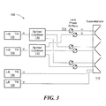
- FIG. 3 shows a further embodiment of a dual band polarization versatile AESLA system 100 in accordance with exemplary embodiments of the invention having an interleaved dual band aperture.
- the system 100 includes a first T/R module 102 for high band horizontal polarization, a second T/R module 104 for high band vertical polarization, a third T/R module 106 for low band horizontal polarization, and a fourth T/R module 108 for low band vertical polarization.
- a first splitter/combiner 110 receives the high band horizontal signal and provides first, second, and third outputs.
- a second splitter/combiner 112 receives the high band vertical signal and provides first, second, and third outputs.
- Pairs of outputs from the first and second splitter/combiners 110 , 112 are provided to respective lens phase shifters 114 , which are coupled to the interleaved radiator assembly 116 .
- the diplexers of the previous embodiment are eliminated and the high band and low band frequencies have separate paths to an interleaved radiator assembly 116 .
- FIG. 4 is a graph showing the low band phase shift using the scan compensation of FIG. 2 .
- the total low band phase shift 90 is the sum of the low band T/R module phase shift 92 plus the perturbation 94 from the lens phase shifters 68 - 73 .
- the compensation is exact at the center of each radiator super-element, but there is a quantized phase error at the other radiator elements, increasing towards the edges of the super-element.
- FIG. 5 in conjunction with FIG. 1 shows an exemplary sequence of steps for implementing a polarization versatile active electronically scanned lens array having a full field of view in accordance with exemplary embodiments of the invention.
- a first signal at a first frequency band and a first polarization is provided by a first transmit/receive module 12 .
- the first signal is split by a splitter/combiner 20 into multiple output signals.
- the splitter/combiner output signals are provided to lens phase shifters 28 , 30 , 32 .
- a second signal at the first frequency band at a second polarization orthogonal to the first polarization is provided by a second transmit/receive module 13 .
- the second signal is split by a splitter/combiner 21 into multiple output signals.
- the split signals are provided to lens phase shifters 29 , 31 , 33 .
- a third signal at a second frequency band at the first polarization is provided by a third transmit/receive module 14 .
- the third signal is split by a splitter/combiner 22 into multiple output signals.
- a fourth signal at the second frequency band and the second polarization is provided by a fourth transmit/receive module 23 .
- the fourth signal is split by a splitter/combiner 23 into multiple output signals.
- a series of diplexers 40 - 45 receive the phase shifter outputs for the first frequency band signals and the split signals from the second frequency band splitter/combiners 22 , 23 .
- signals from the diplexers 40 - 45 are provided to respective radiator elements in a radiator assembly 49 .
- diplexers receive signals from the transmit/receive modules and provide outputs to splitter/combiners, which provide outputs to a lens phase shifters, as shown in FIG. 2 .
- Phase compensators can be provided for the low band transmit/receive modules.
- the diplexers are eliminated by interleaving the signal to the radiator assembly, as shown in FIG. 3 .
Abstract
Description
Φ=−(2π/λL)X M sin(θH)
where λL is the low band wavelength, XM is the position of the super-element phase center, and θH is the high band beam steer angle. For a phase shifter with broadband flat frequency response, such as a high-pass/low-pass design topology, the required compensation phase is:
Φ=−(2π/λH)X M sin(θH)
where λH is the high band wavelength.
Claims (13)
Priority Applications (1)
| Application Number | Priority Date | Filing Date | Title |
|---|---|---|---|
| US12/473,433 US7808427B1 (en) | 2009-05-28 | 2009-05-28 | Radar system having dual band polarization versatile active electronically scanned lens array |
Applications Claiming Priority (1)
| Application Number | Priority Date | Filing Date | Title |
|---|---|---|---|
| US12/473,433 US7808427B1 (en) | 2009-05-28 | 2009-05-28 | Radar system having dual band polarization versatile active electronically scanned lens array |
Publications (1)
| Publication Number | Publication Date |
|---|---|
| US7808427B1 true US7808427B1 (en) | 2010-10-05 |
Family
ID=42797781
Family Applications (1)
| Application Number | Title | Priority Date | Filing Date |
|---|---|---|---|
| US12/473,433 Active US7808427B1 (en) | 2009-05-28 | 2009-05-28 | Radar system having dual band polarization versatile active electronically scanned lens array |
Country Status (1)
| Country | Link |
|---|---|
| US (1) | US7808427B1 (en) |
Cited By (14)
| Publication number | Priority date | Publication date | Assignee | Title |
|---|---|---|---|---|
| US8570237B2 (en) * | 2011-02-01 | 2013-10-29 | Raytheon Company | Multi-band electronically scanned array antenna |
| US8907842B1 (en) | 2009-03-25 | 2014-12-09 | Raytheon Company | Method and apparatus for attenuating a transmitted feedthrough signal |
| US9019153B1 (en) * | 2011-12-20 | 2015-04-28 | Raytheon Company | Calibration of large phased arrays using fourier gauge |
| US9070964B1 (en) | 2011-12-19 | 2015-06-30 | Raytheon Company | Methods and apparatus for volumetric coverage with image beam super-elements |
| US9086476B1 (en) | 2009-03-25 | 2015-07-21 | Raytheon Company | Method and apparatus for rejecting intermodulation products |
| US9373888B1 (en) | 2009-03-25 | 2016-06-21 | Raytheon Company | Method and apparatus for reducing sidelobes in large phased array radar with super-elements |
| US9379446B1 (en) | 2013-05-01 | 2016-06-28 | Raytheon Company | Methods and apparatus for dual polarized super-element phased array radiator |
| CN109669162A (en) * | 2018-12-24 | 2019-04-23 | 中国电子科技集团公司第二十研究所 | One kind being applied to S-X two waveband pathfinder receive-transmit system |
| US10281571B2 (en) | 2014-08-21 | 2019-05-07 | Raytheon Company | Phased array antenna using stacked beams in elevation and azimuth |
| CN110268579A (en) * | 2017-10-18 | 2019-09-20 | 惠普发展公司,有限责任合伙企业 | Antenna in electronic equipment |
| AU2016418723B2 (en) * | 2016-08-09 | 2019-12-05 | Tongyu Communication Inc. | Antenna unit, multi-array antenna system and base station thereof |
| US11152701B2 (en) * | 2018-06-28 | 2021-10-19 | Metawave Corporation | Phase compensated multi-layer, multi-steering antenna array for millimeter wave applications |
| US11588241B2 (en) * | 2017-11-17 | 2023-02-21 | University Of New Hampshire | Compact switched line phase shifter for a microstrip phased array antenna |
| US11808879B1 (en) * | 2019-05-28 | 2023-11-07 | Raytheon Company | Systems and methods for modular radar systems |
Citations (29)
| Publication number | Priority date | Publication date | Assignee | Title |
|---|---|---|---|---|
| US2851681A (en) * | 1955-03-16 | 1958-09-09 | Sperry Rand Corp | Diversity polarization radar system |
| US3403394A (en) * | 1966-07-19 | 1968-09-24 | Gen Electric | Diversity radar system |
| US3566403A (en) * | 1949-03-08 | 1971-02-23 | Raytheon Co | Polarized radar detection system |
| US3772689A (en) * | 1967-12-06 | 1973-11-13 | Us Army | Radar target discrimination method and apparatus |
| US3849780A (en) * | 1969-03-12 | 1974-11-19 | Rockwell International Corp | Dual polarization responsive radar having improved response to small targets |
| US4005425A (en) * | 1975-11-14 | 1977-01-25 | General Motors Corporation | Dual quadrature polarization radar system |
| US4035797A (en) * | 1975-11-14 | 1977-07-12 | General Motors Corporation | Polarized radar system for providing target identification and discrimination |
| US4053882A (en) * | 1976-02-23 | 1977-10-11 | The United States Of America As Represented By The Secretary Of The Air Force | Polarization radar method and system |
| US4323899A (en) * | 1980-06-23 | 1982-04-06 | Sperry Corporation | Polarization detector |
| US4323898A (en) * | 1980-06-23 | 1982-04-06 | Sperry Corporation | Polarization detector |
| US4622524A (en) | 1984-02-24 | 1986-11-11 | Ant Nachrichtentechnik Gmbh | Dual band polarization filter comprising orthogonally oriented fin-type conductors |
| US4689627A (en) | 1983-05-20 | 1987-08-25 | Hughes Aircraft Company | Dual band phased antenna array using wideband element with diplexer |
| US4968969A (en) * | 1986-12-30 | 1990-11-06 | Thomson-Csf | Device and method for data transmission and/or acquisition using two cross polarizations of an electromagnetic wave and magnetic recording device |
| US5262788A (en) * | 1986-12-30 | 1993-11-16 | Thomson-Csf | Device and method for data transmission and/or acquisition using two cross polarizations of an electromagnetic wave and magnetic recording device |
| US5264856A (en) * | 1992-03-06 | 1993-11-23 | Westinghouse Electric Corp. | System and method for detecting radiant energy reflected by a length of wire |
| US5485167A (en) | 1989-12-08 | 1996-01-16 | Hughes Aircraft Company | Multi-frequency band phased-array antenna using multiple layered dipole arrays |
| US5500646A (en) * | 1994-07-29 | 1996-03-19 | The United States Of America As Represented By The Department Of Commerce | Simultaneous differential polymetric measurements and co-polar correlation coefficient measurement |
| US5561434A (en) | 1993-06-11 | 1996-10-01 | Nec Corporation | Dual band phased array antenna apparatus having compact hardware |
| US6114998A (en) | 1997-10-01 | 2000-09-05 | Telefonaktiebolaget Lm Ericsson (Publ) | Antenna unit having electrically steerable transmit and receive beams |
| US6473053B1 (en) | 2001-05-17 | 2002-10-29 | Trw Inc. | Dual frequency single polarization feed network |
| US6563470B2 (en) | 2001-05-17 | 2003-05-13 | Northrop Grumman Corporation | Dual band frequency polarizer using corrugated geometry profile |
| US6646599B1 (en) * | 2002-03-15 | 2003-11-11 | Itt Manufacturing Enterprises, Inc. | Open loop array antenna beam steering architecture |
| US6650291B1 (en) | 2002-05-08 | 2003-11-18 | Rockwell Collins, Inc. | Multiband phased array antenna utilizing a unit cell |
| US6803875B1 (en) * | 2002-09-20 | 2004-10-12 | Drs Weather Systems, Inc. | Simulatneous dual polarization radar system |
| US6828932B1 (en) * | 2003-01-17 | 2004-12-07 | Itt Manufacutring Enterprises, Inc. | System for receiving multiple independent RF signals having different polarizations and scan angles |
| US6859163B2 (en) * | 2002-09-20 | 2005-02-22 | Drs Weather Systems, Inc. | Simultaneous dual polarization radar system |
| US7049997B2 (en) * | 2002-09-20 | 2006-05-23 | Enterprise Electronics Corporation | Simultaneous dual polarization radar system |
| US7116275B2 (en) | 2005-01-28 | 2006-10-03 | Lockheed Martin Corporation | Operationally reconfigurable array |
| US7265713B2 (en) | 2005-02-10 | 2007-09-04 | Raytheon Company | Overlapping subarray architecture |
-
2009
- 2009-05-28 US US12/473,433 patent/US7808427B1/en active Active
Patent Citations (29)
| Publication number | Priority date | Publication date | Assignee | Title |
|---|---|---|---|---|
| US3566403A (en) * | 1949-03-08 | 1971-02-23 | Raytheon Co | Polarized radar detection system |
| US2851681A (en) * | 1955-03-16 | 1958-09-09 | Sperry Rand Corp | Diversity polarization radar system |
| US3403394A (en) * | 1966-07-19 | 1968-09-24 | Gen Electric | Diversity radar system |
| US3772689A (en) * | 1967-12-06 | 1973-11-13 | Us Army | Radar target discrimination method and apparatus |
| US3849780A (en) * | 1969-03-12 | 1974-11-19 | Rockwell International Corp | Dual polarization responsive radar having improved response to small targets |
| US4035797A (en) * | 1975-11-14 | 1977-07-12 | General Motors Corporation | Polarized radar system for providing target identification and discrimination |
| US4005425A (en) * | 1975-11-14 | 1977-01-25 | General Motors Corporation | Dual quadrature polarization radar system |
| US4053882A (en) * | 1976-02-23 | 1977-10-11 | The United States Of America As Represented By The Secretary Of The Air Force | Polarization radar method and system |
| US4323899A (en) * | 1980-06-23 | 1982-04-06 | Sperry Corporation | Polarization detector |
| US4323898A (en) * | 1980-06-23 | 1982-04-06 | Sperry Corporation | Polarization detector |
| US4689627A (en) | 1983-05-20 | 1987-08-25 | Hughes Aircraft Company | Dual band phased antenna array using wideband element with diplexer |
| US4622524A (en) | 1984-02-24 | 1986-11-11 | Ant Nachrichtentechnik Gmbh | Dual band polarization filter comprising orthogonally oriented fin-type conductors |
| US4968969A (en) * | 1986-12-30 | 1990-11-06 | Thomson-Csf | Device and method for data transmission and/or acquisition using two cross polarizations of an electromagnetic wave and magnetic recording device |
| US5262788A (en) * | 1986-12-30 | 1993-11-16 | Thomson-Csf | Device and method for data transmission and/or acquisition using two cross polarizations of an electromagnetic wave and magnetic recording device |
| US5485167A (en) | 1989-12-08 | 1996-01-16 | Hughes Aircraft Company | Multi-frequency band phased-array antenna using multiple layered dipole arrays |
| US5264856A (en) * | 1992-03-06 | 1993-11-23 | Westinghouse Electric Corp. | System and method for detecting radiant energy reflected by a length of wire |
| US5561434A (en) | 1993-06-11 | 1996-10-01 | Nec Corporation | Dual band phased array antenna apparatus having compact hardware |
| US5500646A (en) * | 1994-07-29 | 1996-03-19 | The United States Of America As Represented By The Department Of Commerce | Simultaneous differential polymetric measurements and co-polar correlation coefficient measurement |
| US6114998A (en) | 1997-10-01 | 2000-09-05 | Telefonaktiebolaget Lm Ericsson (Publ) | Antenna unit having electrically steerable transmit and receive beams |
| US6473053B1 (en) | 2001-05-17 | 2002-10-29 | Trw Inc. | Dual frequency single polarization feed network |
| US6563470B2 (en) | 2001-05-17 | 2003-05-13 | Northrop Grumman Corporation | Dual band frequency polarizer using corrugated geometry profile |
| US6646599B1 (en) * | 2002-03-15 | 2003-11-11 | Itt Manufacturing Enterprises, Inc. | Open loop array antenna beam steering architecture |
| US6650291B1 (en) | 2002-05-08 | 2003-11-18 | Rockwell Collins, Inc. | Multiband phased array antenna utilizing a unit cell |
| US6803875B1 (en) * | 2002-09-20 | 2004-10-12 | Drs Weather Systems, Inc. | Simulatneous dual polarization radar system |
| US6859163B2 (en) * | 2002-09-20 | 2005-02-22 | Drs Weather Systems, Inc. | Simultaneous dual polarization radar system |
| US7049997B2 (en) * | 2002-09-20 | 2006-05-23 | Enterprise Electronics Corporation | Simultaneous dual polarization radar system |
| US6828932B1 (en) * | 2003-01-17 | 2004-12-07 | Itt Manufacutring Enterprises, Inc. | System for receiving multiple independent RF signals having different polarizations and scan angles |
| US7116275B2 (en) | 2005-01-28 | 2006-10-03 | Lockheed Martin Corporation | Operationally reconfigurable array |
| US7265713B2 (en) | 2005-02-10 | 2007-09-04 | Raytheon Company | Overlapping subarray architecture |
Cited By (15)
| Publication number | Priority date | Publication date | Assignee | Title |
|---|---|---|---|---|
| US8907842B1 (en) | 2009-03-25 | 2014-12-09 | Raytheon Company | Method and apparatus for attenuating a transmitted feedthrough signal |
| US9086476B1 (en) | 2009-03-25 | 2015-07-21 | Raytheon Company | Method and apparatus for rejecting intermodulation products |
| US9373888B1 (en) | 2009-03-25 | 2016-06-21 | Raytheon Company | Method and apparatus for reducing sidelobes in large phased array radar with super-elements |
| US8570237B2 (en) * | 2011-02-01 | 2013-10-29 | Raytheon Company | Multi-band electronically scanned array antenna |
| US9070964B1 (en) | 2011-12-19 | 2015-06-30 | Raytheon Company | Methods and apparatus for volumetric coverage with image beam super-elements |
| US9019153B1 (en) * | 2011-12-20 | 2015-04-28 | Raytheon Company | Calibration of large phased arrays using fourier gauge |
| US9379446B1 (en) | 2013-05-01 | 2016-06-28 | Raytheon Company | Methods and apparatus for dual polarized super-element phased array radiator |
| US10281571B2 (en) | 2014-08-21 | 2019-05-07 | Raytheon Company | Phased array antenna using stacked beams in elevation and azimuth |
| AU2016418723B2 (en) * | 2016-08-09 | 2019-12-05 | Tongyu Communication Inc. | Antenna unit, multi-array antenna system and base station thereof |
| CN110268579A (en) * | 2017-10-18 | 2019-09-20 | 惠普发展公司,有限责任合伙企业 | Antenna in electronic equipment |
| CN110268579B (en) * | 2017-10-18 | 2022-03-04 | 惠普发展公司,有限责任合伙企业 | Antenna in electronic device |
| US11588241B2 (en) * | 2017-11-17 | 2023-02-21 | University Of New Hampshire | Compact switched line phase shifter for a microstrip phased array antenna |
| US11152701B2 (en) * | 2018-06-28 | 2021-10-19 | Metawave Corporation | Phase compensated multi-layer, multi-steering antenna array for millimeter wave applications |
| CN109669162A (en) * | 2018-12-24 | 2019-04-23 | 中国电子科技集团公司第二十研究所 | One kind being applied to S-X two waveband pathfinder receive-transmit system |
| US11808879B1 (en) * | 2019-05-28 | 2023-11-07 | Raytheon Company | Systems and methods for modular radar systems |
Similar Documents
| Publication | Publication Date | Title |
|---|---|---|
| US7808427B1 (en) | Radar system having dual band polarization versatile active electronically scanned lens array | |
| US11715880B2 (en) | Waveguide feed network architecture for wideband, low profile, dual polarized planar horn array antennas | |
| US7372420B1 (en) | Electronically scanned antenna with secondary phase shifters | |
| US5162803A (en) | Beamforming structure for modular phased array antennas | |
| US20070210959A1 (en) | Multi-beam tile array module for phased array systems | |
| US9124361B2 (en) | Scalable, analog monopulse network | |
| US7916083B2 (en) | Vertically integrated electronically steered phased array and method for packaging | |
| CN101573634B (en) | Phase shifting and combining architecture for phased arrays | |
| CA2793316C (en) | An rf feed network for modular active aperture electronically steered arrays | |
| EP2642587B1 (en) | Modular active radiating device for electronically scanned array aerials | |
| US10727923B2 (en) | Multi-antenna beam forming and spatial multiplexing transceiver | |
| US7868828B2 (en) | Partially overlapped sub-array antenna | |
| EP1943698B1 (en) | Phased array antenna systems and methods | |
| US10135153B2 (en) | Phased array antenna panel with configurable slanted antenna rows | |
| US9735469B1 (en) | Integrated time delay unit system and method for a feed manifold | |
| CN106602265B (en) | Beam forming network and input structure, input and output method and three-beam antenna thereof | |
| US20150318622A1 (en) | Interleaved electronically scanned arrays | |
| US9653820B1 (en) | Active manifold system and method for an array antenna | |
| US9899736B2 (en) | Low cost active antenna system | |
| EP2436084A1 (en) | An improved antenna arrangement | |
| US7071872B2 (en) | Common aperture antenna | |
| EP4148899A1 (en) | Phase shift unit, antenna unit, phased array unit and phased array | |
| US20210151876A1 (en) | Integrated circuit and system with tracking | |
| US9755601B1 (en) | Wireless receiver having improved phase shifting schemes with reduced number of phase shifters | |
| EP3644442B1 (en) | Lossless lobing circuit for multi-subarray tracking |
Legal Events
| Date | Code | Title | Description |
|---|---|---|---|
| AS | Assignment |
Owner name: RAYTHEON COMPANY, MASSACHUSETTS Free format text: ASSIGNMENT OF ASSIGNORS INTEREST;ASSIGNORS:SARCIONE, MICHAEL G.;RYPYSC, DANIEL F.;CHANG, KAICHIANG;AND OTHERS;SIGNING DATES FROM 20090519 TO 20090521;REEL/FRAME:022777/0908 |
|
| FEPP | Fee payment procedure |
Free format text: PAYOR NUMBER ASSIGNED (ORIGINAL EVENT CODE: ASPN); ENTITY STATUS OF PATENT OWNER: LARGE ENTITY |
|
| STCF | Information on status: patent grant |
Free format text: PATENTED CASE |
|
| FPAY | Fee payment |
Year of fee payment: 4 |
|
| MAFP | Maintenance fee payment |
Free format text: PAYMENT OF MAINTENANCE FEE, 8TH YEAR, LARGE ENTITY (ORIGINAL EVENT CODE: M1552) Year of fee payment: 8 |
|
| MAFP | Maintenance fee payment |
Free format text: PAYMENT OF MAINTENANCE FEE, 12TH YEAR, LARGE ENTITY (ORIGINAL EVENT CODE: M1553); ENTITY STATUS OF PATENT OWNER: LARGE ENTITY Year of fee payment: 12 |