US7812335B2 - Sidewall structured switchable resistor cell - Google Patents
Sidewall structured switchable resistor cell Download PDFInfo
- Publication number
- US7812335B2 US7812335B2 US12/216,110 US21611008A US7812335B2 US 7812335 B2 US7812335 B2 US 7812335B2 US 21611008 A US21611008 A US 21611008A US 7812335 B2 US7812335 B2 US 7812335B2
- Authority
- US
- United States
- Prior art keywords
- switching element
- resistivity switching
- conductive electrode
- insulating
- sidewall
- Prior art date
- Legal status (The legal status is an assumption and is not a legal conclusion. Google has not performed a legal analysis and makes no representation as to the accuracy of the status listed.)
- Active, expires
Links
Images


Classifications
-
- H—ELECTRICITY
- H10—SEMICONDUCTOR DEVICES; ELECTRIC SOLID-STATE DEVICES NOT OTHERWISE PROVIDED FOR
- H10B—ELECTRONIC MEMORY DEVICES
- H10B63/00—Resistance change memory devices, e.g. resistive RAM [ReRAM] devices
- H10B63/20—Resistance change memory devices, e.g. resistive RAM [ReRAM] devices comprising selection components having two electrodes, e.g. diodes
- H10B63/22—Resistance change memory devices, e.g. resistive RAM [ReRAM] devices comprising selection components having two electrodes, e.g. diodes of the metal-insulator-metal type
-
- H—ELECTRICITY
- H10—SEMICONDUCTOR DEVICES; ELECTRIC SOLID-STATE DEVICES NOT OTHERWISE PROVIDED FOR
- H10N—ELECTRIC SOLID-STATE DEVICES NOT OTHERWISE PROVIDED FOR
- H10N70/00—Solid-state devices without a potential-jump barrier or surface barrier, and specially adapted for rectifying, amplifying, oscillating or switching
- H10N70/20—Multistable switching devices, e.g. memristors
-
- H—ELECTRICITY
- H10—SEMICONDUCTOR DEVICES; ELECTRIC SOLID-STATE DEVICES NOT OTHERWISE PROVIDED FOR
- H10B—ELECTRONIC MEMORY DEVICES
- H10B63/00—Resistance change memory devices, e.g. resistive RAM [ReRAM] devices
- H10B63/20—Resistance change memory devices, e.g. resistive RAM [ReRAM] devices comprising selection components having two electrodes, e.g. diodes
-
- H—ELECTRICITY
- H10—SEMICONDUCTOR DEVICES; ELECTRIC SOLID-STATE DEVICES NOT OTHERWISE PROVIDED FOR
- H10B—ELECTRONIC MEMORY DEVICES
- H10B63/00—Resistance change memory devices, e.g. resistive RAM [ReRAM] devices
- H10B63/80—Arrangements comprising multiple bistable or multi-stable switching components of the same type on a plane parallel to the substrate, e.g. cross-point arrays
-
- H—ELECTRICITY
- H10—SEMICONDUCTOR DEVICES; ELECTRIC SOLID-STATE DEVICES NOT OTHERWISE PROVIDED FOR
- H10N—ELECTRIC SOLID-STATE DEVICES NOT OTHERWISE PROVIDED FOR
- H10N70/00—Solid-state devices without a potential-jump barrier or surface barrier, and specially adapted for rectifying, amplifying, oscillating or switching
- H10N70/011—Manufacture or treatment of multistable switching devices
- H10N70/021—Formation of the switching material, e.g. layer deposition
- H10N70/023—Formation of the switching material, e.g. layer deposition by chemical vapor deposition, e.g. MOCVD, ALD
-
- H—ELECTRICITY
- H10—SEMICONDUCTOR DEVICES; ELECTRIC SOLID-STATE DEVICES NOT OTHERWISE PROVIDED FOR
- H10N—ELECTRIC SOLID-STATE DEVICES NOT OTHERWISE PROVIDED FOR
- H10N70/00—Solid-state devices without a potential-jump barrier or surface barrier, and specially adapted for rectifying, amplifying, oscillating or switching
- H10N70/011—Manufacture or treatment of multistable switching devices
- H10N70/021—Formation of the switching material, e.g. layer deposition
- H10N70/026—Formation of the switching material, e.g. layer deposition by physical vapor deposition, e.g. sputtering
-
- H—ELECTRICITY
- H10—SEMICONDUCTOR DEVICES; ELECTRIC SOLID-STATE DEVICES NOT OTHERWISE PROVIDED FOR
- H10N—ELECTRIC SOLID-STATE DEVICES NOT OTHERWISE PROVIDED FOR
- H10N70/00—Solid-state devices without a potential-jump barrier or surface barrier, and specially adapted for rectifying, amplifying, oscillating or switching
- H10N70/011—Manufacture or treatment of multistable switching devices
- H10N70/061—Patterning of the switching material
- H10N70/068—Patterning of the switching material by processes specially adapted for achieving sub-lithographic dimensions, e.g. using spacers
-
- H—ELECTRICITY
- H10—SEMICONDUCTOR DEVICES; ELECTRIC SOLID-STATE DEVICES NOT OTHERWISE PROVIDED FOR
- H10N—ELECTRIC SOLID-STATE DEVICES NOT OTHERWISE PROVIDED FOR
- H10N70/00—Solid-state devices without a potential-jump barrier or surface barrier, and specially adapted for rectifying, amplifying, oscillating or switching
- H10N70/20—Multistable switching devices, e.g. memristors
- H10N70/231—Multistable switching devices, e.g. memristors based on solid-state phase change, e.g. between amorphous and crystalline phases, Ovshinsky effect
-
- H—ELECTRICITY
- H10—SEMICONDUCTOR DEVICES; ELECTRIC SOLID-STATE DEVICES NOT OTHERWISE PROVIDED FOR
- H10N—ELECTRIC SOLID-STATE DEVICES NOT OTHERWISE PROVIDED FOR
- H10N70/00—Solid-state devices without a potential-jump barrier or surface barrier, and specially adapted for rectifying, amplifying, oscillating or switching
- H10N70/20—Multistable switching devices, e.g. memristors
- H10N70/24—Multistable switching devices, e.g. memristors based on migration or redistribution of ionic species, e.g. anions, vacancies
- H10N70/245—Multistable switching devices, e.g. memristors based on migration or redistribution of ionic species, e.g. anions, vacancies the species being metal cations, e.g. programmable metallization cells
-
- H—ELECTRICITY
- H10—SEMICONDUCTOR DEVICES; ELECTRIC SOLID-STATE DEVICES NOT OTHERWISE PROVIDED FOR
- H10N—ELECTRIC SOLID-STATE DEVICES NOT OTHERWISE PROVIDED FOR
- H10N70/00—Solid-state devices without a potential-jump barrier or surface barrier, and specially adapted for rectifying, amplifying, oscillating or switching
- H10N70/801—Constructional details of multistable switching devices
- H10N70/821—Device geometry
- H10N70/826—Device geometry adapted for essentially vertical current flow, e.g. sandwich or pillar type devices
- H10N70/8265—Device geometry adapted for essentially vertical current flow, e.g. sandwich or pillar type devices on sidewalls of dielectric structures, e.g. mesa or cup type devices
-
- H—ELECTRICITY
- H10—SEMICONDUCTOR DEVICES; ELECTRIC SOLID-STATE DEVICES NOT OTHERWISE PROVIDED FOR
- H10N—ELECTRIC SOLID-STATE DEVICES NOT OTHERWISE PROVIDED FOR
- H10N70/00—Solid-state devices without a potential-jump barrier or surface barrier, and specially adapted for rectifying, amplifying, oscillating or switching
- H10N70/801—Constructional details of multistable switching devices
- H10N70/881—Switching materials
- H10N70/883—Oxides or nitrides
- H10N70/8833—Binary metal oxides, e.g. TaOx
-
- H—ELECTRICITY
- H10—SEMICONDUCTOR DEVICES; ELECTRIC SOLID-STATE DEVICES NOT OTHERWISE PROVIDED FOR
- H10N—ELECTRIC SOLID-STATE DEVICES NOT OTHERWISE PROVIDED FOR
- H10N70/00—Solid-state devices without a potential-jump barrier or surface barrier, and specially adapted for rectifying, amplifying, oscillating or switching
- H10N70/801—Constructional details of multistable switching devices
- H10N70/881—Switching materials
- H10N70/883—Oxides or nitrides
- H10N70/8836—Complex metal oxides, e.g. perovskites, spinels
-
- H—ELECTRICITY
- H10—SEMICONDUCTOR DEVICES; ELECTRIC SOLID-STATE DEVICES NOT OTHERWISE PROVIDED FOR
- H10N—ELECTRIC SOLID-STATE DEVICES NOT OTHERWISE PROVIDED FOR
- H10N70/00—Solid-state devices without a potential-jump barrier or surface barrier, and specially adapted for rectifying, amplifying, oscillating or switching
- H10N70/801—Constructional details of multistable switching devices
- H10N70/881—Switching materials
- H10N70/884—Other compounds of groups 13-15, e.g. elemental or compound semiconductors
- H10N70/8845—Carbon or carbides
Definitions
- the invention generally relates to a method of making a semiconductor device, and more particularly, to a method of making a semiconductor nonvolatile memory cell.
- Memory circuits are the backbone of such devices as data and instruction sets are stored therein. Maximizing the number of memory elements per unit area on such circuits minimizes their cost and thus is a primary motivation in the designing of such circuits.
- FIG. 1 illustrates an exemplary prior art memory cell 20 which includes a vertically oriented, cylindrical pillar shaped junction diode 22 as the steering element of the cell and a storage element 24 , such as an antifuse dielectric or a metal oxide resistivity switching layer.
- the diode 22 and the storage element 24 are interposed between top 26 and bottom 28 conductors or electrodes.
- the vertically oriented junction diode 22 includes a heavily doped semiconductor region 30 of a first conductivity type (such as n-type), an intermediate region 32 which is undoped semiconductor material or lightly doped semiconductor material (which will be referred to as an intrinsic region), and a heavily doped semiconductor region 34 of the second conductivity type (such as p-type) to form a p-i-n diode.
- a first conductivity type such as n-type
- an intermediate region 32 which is undoped semiconductor material or lightly doped semiconductor material (which will be referred to as an intrinsic region)
- the semiconductor material of the junction diode 22 is generally silicon, germanium, or an alloy of silicon and/or germanium. Other semiconductor materials may also be used.
- the junction diode 22 and the storage element 24 are arranged in series between the bottom conductor 28 and the top conductor 26 , which may be formed of a metal, such as tungsten and/or TiN.
- the storage element 24 may be located above or below the diode 22 . Referring to FIG. 1A , U.S. Pat. No. 6,952,030, issued to Herner et al. and entitled “High-Density Three-Dimensional Memory Cell,” hereinafter the “'030 patent” and hereby incorporated by reference in its entirety, discloses an exemplary nonvolatile memory cell.
- the resistance of metal oxide switchable resistors can be too low to be efficiently sensed by a three dimensional (3D) diode array.
- a low reset current is generally preferable to a high reset current, and thus the resistance of the resistor element is generally preferred to be high.
- the metal oxide element 24 is disposed over a diode pillar 22 , the resistance of the oxide element can be too low, thereby giving rise to an undesirably high reset current.
- the metal oxide resistor material can be damaged as a result of etching during fabrication and thus fails to provide switching function.
- a method of making a memory device includes forming a first conductive electrode, forming an insulating structure over the first conductive electrode, forming a resistivity switching element on a sidewall of the insulating structure, forming a second conductive electrode over the resistivity switching element, and forming a steering element in series with the resistivity switching element between the first conductive electrode and the second conductive electrode, wherein a height of the resistivity switching element in a first direction from the first conductive electrode to the second conductive electrode is greater than a thickness of the resistivity switching element in second direction perpendicular to the first direction.
- FIG. 1A illustrates a three dimensional view of a prior art memory cell.
- FIGS. 1B and 1C show the side view and top view, respectively, of the resistivity switching storage element of the prior art cell.
- FIGS. 2A and 2B show the side view and top view, respectively of a cell according to an embodiment of the invention.
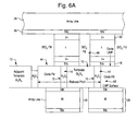
- FIGS. 3 , 4 , 5 , 6 A and 7 illustrate side cross sectional views of memory cells according to embodiments of the invention.
- FIG. 6B is a top view of the cell of FIG. 6A .
- the resistance of the storage element which is also referred to as a resistivity switching element herein, can be increased by a geometry effect, where the resistivity switching element is formed on a sidewall of the insulating structure in series with the steering element.
- the height of the resistivity switching element in a “vertical” direction from the bottom conductive electrode to the upper conductive electrode is greater than a thickness of the resistivity switching element in a second direction perpendicular to the “vertical” direction.
- the resistivity switching element can be a thin layer of binary metal oxide located on the sidewall of an insulating structure and still be provided in series with a diode steering element between the lower and upper electrodes.
- ⁇ is the resistivity of the material
- t the height of the layer
- (L*W) the area of the conductive path.
- FIGS. 1B , 1 C, 2 A and 2 B illustrate such dependence of the resistance.
- FIGS. 1B and 1C illustrate the resistivity switching element 24 located on top of the diode (which is omitted from FIGS. 1B and 1C for clarity but can be located above or below element 24 ).
- the resistance of the conductive filament may be a relatively low resistance.
- Typical metal oxide switchable resistance materials may form filaments that have resistance in the 1 K ohm to 10 K ohm range which is lower resistance than typically achieved by diodes formed for use in three dimensional diode arrays. The diodes in three dimensional diode arrays may not reliably reset relatively low resistance filaments.
- FIGS. 2A and 2B illustrate side cross sectional and top views of a portion of a memory cell structure according to one embodiment of the invention, where the diode is again omitted for clarity, but which is located above or below and in series with the resistivity switching element 14 between electrodes 26 and 28 .
- the resistivity switching element 14 is formed on a sidewall of an insulating structure 13 .
- Length l can be significantly smaller than length L of FIGS. 1B and 1C .
- the resistance increases by a factor of (L/l) in the configuration of FIGS.
- Height, T is the height of the resistivity switching element 14 which covers the sidewall of the insulating structure 13 .
- Height T can be equal to the prior planar thickness, t and in some cases can be greater than planar thickness, t, of FIGS. 1B and 1C .
- FIGS. 2A and 2B One advantage of the embodiment of the invention shown in FIGS. 2A and 2B is the increase of the low resistance state which depends on the magnitude of height T. Note that the region that switches to high resistance could be less than T as shown in FIG. 3 for some materials.
- W tends to be greater than t in the prior art configuration shown in FIGS. 1B and 1C , and less than T in the sidewall configuration of the embodiments of the invention shown in FIGS. 2A and 2B .
- the thickness of the sidewall layer l can be less than the typical dimension of the filamentary region. Since l can be smaller than the prior art filament diameter, it also tends to reduce the extent of the filament in the W dimension in some materials for further resistance increase.
- the resistance of the resistivity switching element in the embodiments of the invention is less dependent on the size of the variable filament formation because it is restricted by the dimension l. Since the cross-sectional area of the current path through the resistivity switching element is restricted to less than the typical filament size in some materials, the reset current will also be lower. Reduced reset current and the associated IR drops in the switch and array lines is a significant advantage in allowing the reset voltage and power to decrease in memory arrays comprising the sidewall resistivity switching elements.
- the diodes in three dimensional diode arrays may reliably reset the relatively high resistance filaments formed in the embodiments of the invention.
- the L tends to increase with t and may be about four times t, for example t is 5 nm and L is 20 nm.
- 1 is insensitive to T so that T can be increased by process choices; for example, the height, T, of the resistivity switching material layer can be greater than 5 nm, such as greater than 20 nm, and the thickness l can be less than 20 nm, such as less than 5 nm.
- the resistance can be increased from that illustrated in FIG. 1 by a factor of (L/l) times (T/t) for an increase of 16 times in this example.
- FIGS. 3-7 illustrate exemplary memory cell structures with various insulating structures 13 according to the embodiments of the invention.
- the resistivity switching element 14 can have different shapes. For example, it can be annular, surrounding the insulating structure or it can be located inside a trench in an insulating material.
- the insulating structure can have different shapes, such as a pillar or rail shape.
- the pillar diode 22 (shown in detail in FIG. 1A ) is formed over the lower electrode 28 (which is also shown in FIG. 1 ).
- the diode 22 can made of any suitable semiconductor material, such as silicon, germanium, SiGe or other compound semiconductor materials, which can be polycrystalline, single crystalline, or amorphous.
- the electrode 28 is located on or over a substrate, such as a semiconductor wafer (including silicon or compound semiconductor wafers), or a glass, plastic or metal substrate.
- the electrode 28 may comprise a metal such as tungsten, aluminum or their alloys, or a metallic compound, such as titanium nitride.
- the barrier 16 may comprise any conductive material, such as titanium nitride.
- the insulating structure 13 is formed over the barrier 16 .
- the insulating structure 13 can comprise any suitable insulating material, such as silicon oxide or silicon nitride or an organic insulating material.
- the structure 13 may have any suitable shape, such as rail or pillar shape, as long as it contains a sidewall 15 .
- At least one resistivity switching element 14 is then formed on at least one sidewall of the insulating structure 13 . If the structure is cylindrical, as shown in FIG. 2B , then it has only one sidewall 15 .
- the resistivity switching element 14 can comprise a fuse, polysilicon memory effect material, a metal oxide (such as binary metal oxide, for example nickel oxide, or a switchable complex metal oxide, such as perovskite oxide), carbon nanotubes, graphene switchable resistance material, other carbon resistivity switching material, such as amorphous, polycrystalline or microcrystalline carbon, phase change materials, electrolyte switching materials, switchable complex metal oxides, conductive bridge elements, or switchable polymers.
- the resistivity of the resistivity switching element may be increased or decreased in response to a forward and/or reverse bias provided between the electrodes 26 and 28 shown in FIG. 1A .
- the resistivity switching element 14 can be formed on the insulating structure 13 by any suitable methods, such as chemical vapor deposition, physical vapor deposition (such as sputtering), etc.
- the element 14 can be located over the top surface of the insulating structure 13 and on the sidewall 15 of the insulating structure 13 .
- the element 14 such as a metal oxide insulating layer, is formed over the insulating structure 13 and then planarized by CMP or other methods to remove the thickness Lo of element 14 located on the upper surface of the structure 13 and to expose an upper surface of insulating structure 13 .
- the active switching region 18 of the element 14 has a length L which may be thinner than the planar thickness of the element due to shadowing effects of PVD deposition. This sidewall necking in region 18 increases the resistance of the element 14 .
- a metal or metal nitride film such as titanium nitride film, is deposited over the structure 13 and subsequently selectively removed from the top of insulating structure by CMP or other planarization methods.
- the patterned film is then oxidized in an oxidizing ambient thereby forming a metal oxide or oxynitride resistivity switching element 14 , for example a titanium oxynitride element. Due to the above described necking, the active region 18 of the element may be completely converted to an insulating metal oxide or oxynitride, while the upper portion 42 of the element 14 may remain as a conductive metal or metal nitride.
- the thickness of the element 14 is expanded for clarity in FIG. 4 .
- Element 14 may have a vertical thickness of 10 to 30 nm.
- the sidewalls 15 of the structure 13 comprise sidewall(s) of a hole or trench 42 formed in an insulating layer 13 , such as a silicon oxide layer.
- the hole or trench exposes the bottom electrode 28 to allow the resistivity switching material to electrically contact the bottom electrode 28 .
- the groove remaining in the resistivity switching element 14 may be filled with an insulating filler material 44 , such as a silicon oxide or organic material, and planarized by CMP or other suitable methods, to expose the upper surface of the element 14 .
- the bottom electrode 28 may comprise a combination of TiN and tungsten layers.
- the diode 22 is located above the resistivity switching element 14 and barrier 16 . However, the order may be reversed and the diode 22 may be formed below the barrier 16 and element 14 .
- an upper barrier 46 may be formed between the diode 22 and the upper electrode 26 .
- the upper barrier 46 may comprise a titanium silicide layer, such as a C49 phase titanium silicide layer formed by reacting a titanium layer with the polysilicon material of the diode, and a Ti/TiN bilayer.
- the diode 22 acts as a steering element of the cell.
- the memory cell can include a vertically oriented, cylindrical pillar shaped junction diode.
- junction diode is used herein to refer to a semiconductor device with the property of non-ohmic conduction, having two terminal electrodes, and made of semiconducting material which is p-type at one electrode and n-type at the other.
- Examples include p-n diodes and n-p diodes, which have a p-type semiconductor material and an n-type semiconductor material in contact, such as Zener diodes, and p-i-n diodes, in which an intrinsic (undoped) semiconductor material is interposed between the p-type semiconductor material and the n-type semiconductor material.
- a tunneling diode comprising MIM or MIIM structures may be used.
- the resistivity switching element 14 comprises an insulating layer, such as a metal oxide layer (for example Al 2 O 3 ) which is deposited in an insulating state inside the hole or trench 42 (instead of oxidizing a conductive layer as shown in FIG. 4 ).
- the element is formed using a Damascene type process.
- the insulating layer which forms the element 14 does not necessarily have to be planarized and can extend over the structure 13 .
- the diode 22 may be offset with respect to the element 14 to make sure that element 14 contacts the diode 22 .
- the element 14 can be 5-30 nm high, while the electrode 28 may be about 200 nm high.
- the insulating structure 13 can comprise insulating rail shaped structures 13 .
- the rails may be formed by patterning an insulating layer, such as silicon oxide or nitride into insulating structure rails 13 .
- the rails 13 may extend in the same direction as lower electrodes 28 (such as TiN/W/TiN electrodes for example).
- the rails 13 are offset from the electrodes 28 such that sidewalls 15 of each rail 13 are located over the upper surfaces of adjacent electrodes 28 .
- the resistivity switching element 14 is then formed on the sidewalls 15 of the rails 13 .
- the bottom electrodes 28 are exposed between adjacent rails 13 .
- element 14 may be formed by depositing a metal oxide layer over the rails 13 and then planarizing the metal oxide layer.
- the metal oxide layer may be recessed below the upper surface of the rails where there are no diodes 22 formed over the metal layer.
- the space between the rails 13 may be filled with an insulating filler material 44 , such as silicon oxide, followed by CMP or other planarization.
- the space between the diodes 22 may also be filled with the planarized filler material 48 .
- the memory device can be formed by forming at least one diode 22 over the bottom electrode 28 . Subsequently, the barrier layer 16 and the insulating structure 13 , such as a cylindrical pillar structure 13 , are formed over the diode. The resistivity switching element 14 is formed on the sidewall 15 of the structure 13 .
- the structure 13 may be formed by forming a hard mask pattern layer over an insulating template layer.
- the hard mask layer can comprise tungsten or amorphous carbon or other material.
- the template layer can be selectively removed by any suitable method, such as isotropic etching, using the hard mask pattern as a mask to undercut the hard mask pattern. As a result, the width of the template layer is reduced, and at least one insulating pillar is formed from the template layer. This forms a “mushroom” shape of an insulating structure 13 pillar stem covered with a larger diameter hard mask cap.
- Resistivity switching material such as a metal oxide layer
- Resistivity switching material is then subsequently deposited over a sidewall of the insulating structure 13 pillar and on the hard mask cap by any suitable methods, such as for example atomic layer deposition.
- the semiconductor diode layer(s) (and optionally the barrier layer 16 ) can be selectively etched using the hard mask pattern as a mask to form at least one pillar diode steering element (and optionally a patterned barrier 16 ).
- the hard mask pattern layer can be optionally removed before the upper electrode 26 is formed contact with the resistivity switching element 14 or the hard mask may be retained as part of the upper electrode 26 if the hard mask is electrically conductive.
- the diode has the same diameter as the hard mask pattern, while the insulating structure 13 has a smaller diameter (or width) than the diode due to the isotropic etching and undercutting. This allows the edge of the resistivity switching element 14 to directly or indirectly electrically contact the diode 22 below structure 13 and to directly or indirectly electrically contact the upper electrode 26 located above structure 13 .
- the memory cell of the embodiments of the invention may comprise a one-time programmable (OTP) or re-writable nonvolatile memory cell, and may be selected from at least one of antifuse, fuse, diode and antifuse arranged in a series, polysilicon memory effect cell, metal oxide memory, switchable complex metal oxide, carbon nanotube memory, graphene or other carbon switchable resistance material, phase change material memory, conductive bridge element, or switchable polymer memory.
- OTP one-time programmable
- re-writable nonvolatile memory cell may be selected from at least one of antifuse, fuse, diode and antifuse arranged in a series, polysilicon memory effect cell, metal oxide memory, switchable complex metal oxide, carbon nanotube memory, graphene or other carbon switchable resistance material, phase change material memory, conductive bridge element, or switchable polymer memory.
- Formation of a first memory level has been described. Additional memory levels can be formed above this first memory level to form a monolithic three dimensional memory array.
- conductors can be shared between memory levels; i.e. top conductor would serve as the bottom conductor of the next memory level.
- an interlevel dielectric (not shown) is formed above the first memory level, its surface planarized, and construction of a second memory level begins on this planarized interlevel dielectric, with no shared conductors.
- a monolithic three dimensional memory array is one in which multiple memory levels are formed above a single substrate, such as a wafer, with no intervening substrates.
- the layers forming one memory level are deposited or grown directly over the layers of an existing level or levels.
- stacked memories have been constructed by forming memory levels on separate substrates and adhering the memory levels atop each other, as in Leedy, U.S. Pat. No. 5,915,167, “Three dimensional structure memory.”
- the substrates may be thinned or removed from the memory levels before bonding, but as the memory levels are initially formed over separate substrates, such memories are not true monolithic three dimensional memory arrays.
- a monolithic three dimensional memory array formed above a substrate comprises at least a first memory level formed at a first height above the substrate and a second memory level formed at a second height different from the first height. Three, four, eight, or indeed any number of memory levels can be formed above the substrate in such a multilevel array.
- one layer has been described as being “above” or “below” another. It will be understood that these terms describe the position of layers and elements relative to the substrate upon which they are formed, in most embodiments a monocrystalline silicon wafer substrate; one feature is above another when it is farther from the wafer substrate, and below another when it is closer. Though clearly the wafer, or the die, can be rotated in any direction, the relative orientation of first features on the wafer or die will not change.
- the drawings are purposefully not shown to scale and are merely representative of layers and processed layers.
Abstract
Description
R=ρ*t/(L*W), [1]
where ρ is the resistivity of the material, t the height of the layer, (L*W) the area of the conductive path. As a result, the resistance of the layer can be highly dependent on geometry.
R=ρ*T/(l*W) [2]
where l is the deposited thickness of
Claims (8)
Priority Applications (9)
| Application Number | Priority Date | Filing Date | Title |
|---|---|---|---|
| US12/216,110 US7812335B2 (en) | 2008-04-11 | 2008-06-30 | Sidewall structured switchable resistor cell |
| CN2012105722908A CN102983273A (en) | 2008-04-11 | 2009-04-01 | Sidewall structured switchable resistor cell |
| JP2011504064A JP5044042B2 (en) | 2008-04-11 | 2009-04-01 | Side wall structured switchable resistor cell |
| EP09731080A EP2277201A1 (en) | 2008-04-11 | 2009-04-01 | Sidewall structured switchable resistor cell |
| PCT/US2009/039126 WO2009126492A1 (en) | 2008-04-11 | 2009-04-01 | Sidewall structured switchable resistor cell |
| CN200980112695.XA CN101999170B (en) | 2008-04-11 | 2009-04-01 | Sidewall structured switchable resistor cell |
| KR1020107024382A KR101532203B1 (en) | 2008-04-11 | 2009-04-01 | Sidewall structured switchable resistor cell |
| TW098112104A TWI380437B (en) | 2008-04-11 | 2009-04-10 | Sidewall structured switchable resistor cell |
| JP2012130412A JP5395213B2 (en) | 2008-04-11 | 2012-06-08 | Side wall structured switchable resistor cell |
Applications Claiming Priority (2)
| Application Number | Priority Date | Filing Date | Title |
|---|---|---|---|
| US7109308P | 2008-04-11 | 2008-04-11 | |
| US12/216,110 US7812335B2 (en) | 2008-04-11 | 2008-06-30 | Sidewall structured switchable resistor cell |
Publications (2)
| Publication Number | Publication Date |
|---|---|
| US20090256129A1 US20090256129A1 (en) | 2009-10-15 |
| US7812335B2 true US7812335B2 (en) | 2010-10-12 |
Family
ID=40839545
Family Applications (1)
| Application Number | Title | Priority Date | Filing Date |
|---|---|---|---|
| US12/216,110 Active 2028-08-21 US7812335B2 (en) | 2008-04-11 | 2008-06-30 | Sidewall structured switchable resistor cell |
Country Status (7)
| Country | Link |
|---|---|
| US (1) | US7812335B2 (en) |
| EP (1) | EP2277201A1 (en) |
| JP (2) | JP5044042B2 (en) |
| KR (1) | KR101532203B1 (en) |
| CN (2) | CN101999170B (en) |
| TW (1) | TWI380437B (en) |
| WO (1) | WO2009126492A1 (en) |
Cited By (12)
| Publication number | Priority date | Publication date | Assignee | Title |
|---|---|---|---|---|
| US20100006812A1 (en) * | 2008-07-08 | 2010-01-14 | Sandisk 3D Llc | Carbon-based resistivity-switching materials and methods of forming the same |
| US20100163824A1 (en) * | 2008-12-31 | 2010-07-01 | Huiwen Xu | Modulation of resistivity in carbon-based read-writeable materials |
| US20110133149A1 (en) * | 2009-12-04 | 2011-06-09 | Sonehara Takeshi | Resistance change memory and manufacturing method thereof |
| US20120032140A1 (en) * | 2009-09-18 | 2012-02-09 | Jingjing Li | Light-emitting diode including a metal-dielectric-metal structure |
| US20130163306A1 (en) * | 2010-07-15 | 2013-06-27 | Fudan University | One-Time Programmable Memory Cell, Memory and Manufacturing Method Thereof |
| US8742389B2 (en) | 2012-01-27 | 2014-06-03 | Samsung Electronics Co., Ltd. | Variable resistance memory device and method of forming the same |
| US9276204B2 (en) | 2012-02-29 | 2016-03-01 | Hewlett Packard Enterprise Development Lp | Memristor with channel region in thermal equilibrium with containing region |
| US9373664B2 (en) | 2014-07-28 | 2016-06-21 | Samsung Electronics Co., Ltd. | Variable resistance memory devices and methods of manufacturing the same |
| US9806256B1 (en) | 2016-10-21 | 2017-10-31 | Sandisk Technologies Llc | Resistive memory device having sidewall spacer electrode and method of making thereof |
| US10062842B2 (en) | 2015-01-30 | 2018-08-28 | Hewlett Packard Enterprise Development Lp | Composite selector electrodes |
| US10991879B2 (en) | 2019-06-26 | 2021-04-27 | Western Digital Technologies, Inc. | Multi-level phase change memory cells and method of making the same |
| US11239416B2 (en) | 2019-05-03 | 2022-02-01 | Samsung Electronics Co., Ltd. | Variable resistance memory device |
Families Citing this family (17)
| Publication number | Priority date | Publication date | Assignee | Title |
|---|---|---|---|---|
| US7830698B2 (en) * | 2008-04-11 | 2010-11-09 | Sandisk 3D Llc | Multilevel nonvolatile memory device containing a carbon storage material and methods of making and using same |
| US8374018B2 (en) * | 2010-07-09 | 2013-02-12 | Crossbar, Inc. | Resistive memory using SiGe material |
| JP5572056B2 (en) * | 2010-10-20 | 2014-08-13 | 株式会社東芝 | Storage device and manufacturing method thereof |
| US8502185B2 (en) * | 2011-05-31 | 2013-08-06 | Crossbar, Inc. | Switching device having a non-linear element |
| US8482078B2 (en) | 2011-05-10 | 2013-07-09 | International Business Machines Corporation | Integrated circuit diode |
| US8394682B2 (en) | 2011-07-26 | 2013-03-12 | Micron Technology, Inc. | Methods of forming graphene-containing switches |
| US8879299B2 (en) | 2011-10-17 | 2014-11-04 | Sandisk 3D Llc | Non-volatile memory cell containing an in-cell resistor |
| KR20130043533A (en) * | 2011-10-20 | 2013-04-30 | 삼성전자주식회사 | Non-volatile memory device having conductive buffer pattern and method of forming the same |
| US8710481B2 (en) | 2012-01-23 | 2014-04-29 | Sandisk 3D Llc | Non-volatile memory cell containing a nano-rail electrode |
| US8658476B1 (en) | 2012-04-20 | 2014-02-25 | Crossbar, Inc. | Low temperature P+ polycrystalline silicon material for non-volatile memory device |
| JPWO2014050198A1 (en) * | 2012-09-28 | 2016-08-22 | 日本電気株式会社 | Switching element and method for manufacturing switching element |
| CN104051619B (en) * | 2013-03-13 | 2017-07-04 | 旺宏电子股份有限公司 | Memory cell with phase-change element and forming method thereof |
| US9093635B2 (en) * | 2013-03-14 | 2015-07-28 | Crossbar, Inc. | Controlling on-state current for two-terminal memory |
| KR101458566B1 (en) * | 2013-05-21 | 2014-11-07 | 재단법인대구경북과학기술원 | Rectifying device and and method for manufacturing the same |
| KR102474306B1 (en) * | 2018-02-20 | 2022-12-06 | 에스케이하이닉스 주식회사 | cross-point array device and method of fabricating the same |
| CN112018234B (en) * | 2020-07-22 | 2021-10-15 | 厦门半导体工业技术研发有限公司 | Semiconductor device and method for manufacturing semiconductor device |
| DE112021007796T5 (en) * | 2021-06-09 | 2024-04-18 | Microchip Technology Incorporated | CARBON NANORUBE (CNT) MEMORY CELL ELEMENT AND DESIGN METHOD |
Citations (88)
| Publication number | Priority date | Publication date | Assignee | Title |
|---|---|---|---|---|
| US4646266A (en) | 1984-09-28 | 1987-02-24 | Energy Conversion Devices, Inc. | Programmable semiconductor structures and methods for using the same |
| US4665428A (en) | 1984-01-13 | 1987-05-12 | The British Petroleum Company P.L.C. | Semiconductor device |
| US5166760A (en) | 1990-02-28 | 1992-11-24 | Hitachi, Ltd. | Semiconductor Schottky barrier device with pn junctions |
| US5432729A (en) | 1993-04-23 | 1995-07-11 | Irvine Sensors Corporation | Electronic module comprising a stack of IC chips each interacting with an IC chip secured to the stack |
| US5559732A (en) | 1994-12-27 | 1996-09-24 | Syracuse University | Branched photocycle optical memory device |
| US5693556A (en) | 1995-12-29 | 1997-12-02 | Cypress Semiconductor Corp. | Method of making an antifuse metal post structure |
| US5745407A (en) | 1994-05-05 | 1998-04-28 | California Institute Of Technology | Transistorless, multistable current-mode memory cells and memory arrays and methods of reading and writing to the same |
| US5751012A (en) | 1995-06-07 | 1998-05-12 | Micron Technology, Inc. | Polysilicon pillar diode for use in a non-volatile memory cell |
| US5835396A (en) | 1996-10-17 | 1998-11-10 | Zhang; Guobiao | Three-dimensional read-only memory |
| US5915167A (en) | 1997-04-04 | 1999-06-22 | Elm Technology Corporation | Three dimensional structure memory |
| US5962911A (en) | 1996-04-29 | 1999-10-05 | Vlsi Technology, Inc. | Semiconductor devices having amorphous silicon antifuse structures |
| US5991193A (en) | 1997-12-02 | 1999-11-23 | International Business Machines Corporation | Voltage biasing for magnetic ram with magnetic tunnel memory cells |
| US6014330A (en) | 1993-06-29 | 2000-01-11 | Kabushiki Kaisha Toshiba | Non-volatile semiconductor memory device |
| US6034882A (en) | 1998-11-16 | 2000-03-07 | Matrix Semiconductor, Inc. | Vertically stacked field programmable nonvolatile memory and method of fabrication |
| US6055180A (en) | 1997-06-17 | 2000-04-25 | Thin Film Electronics Asa | Electrically addressable passive device, method for electrical addressing of the same and uses of the device and the method |
| US6111784A (en) | 1997-09-18 | 2000-08-29 | Canon Kabushiki Kaisha | Magnetic thin film memory element utilizing GMR effect, and recording/reproduction method using such memory element |
| US6187617B1 (en) | 1999-07-29 | 2001-02-13 | International Business Machines Corporation | Semiconductor structure having heterogeneous silicide regions and method for forming same |
| US6236587B1 (en) | 1997-09-01 | 2001-05-22 | Thin Film Electronics Asa | Read-only memory and read-only memory devices |
| US6306718B1 (en) | 2000-04-26 | 2001-10-23 | Dallas Semiconductor Corporation | Method of making polysilicon resistor having adjustable temperature coefficients |
| US6420215B1 (en) | 2000-04-28 | 2002-07-16 | Matrix Semiconductor, Inc. | Three-dimensional memory array and method of fabrication |
| US6483736B2 (en) | 1998-11-16 | 2002-11-19 | Matrix Semiconductor, Inc. | Vertically stacked field programmable nonvolatile memory and method of fabrication |
| US6486065B2 (en) | 2000-12-22 | 2002-11-26 | Matrix Semiconductor, Inc. | Method of forming nonvolatile memory device utilizing a hard mask |
| US6525953B1 (en) | 2001-08-13 | 2003-02-25 | Matrix Semiconductor, Inc. | Vertically-stacked, field-programmable, nonvolatile memory and method of fabrication |
| US6541312B2 (en) | 2000-12-22 | 2003-04-01 | Matrix Semiconductor, Inc. | Formation of antifuse structure in a three dimensional memory |
| US6548313B1 (en) | 2002-05-31 | 2003-04-15 | Intel Corporation | Amorphous carbon insulation and carbon nanotube wires |
| US6567301B2 (en) | 2001-08-09 | 2003-05-20 | Hewlett-Packard Development Company, L.P. | One-time programmable unit memory cell based on vertically oriented fuse and diode and one-time programmable memory using the same |
| US6574130B2 (en) | 2001-07-25 | 2003-06-03 | Nantero, Inc. | Hybrid circuit having nanotube electromechanical memory |
| US6584029B2 (en) | 2001-08-09 | 2003-06-24 | Hewlett-Packard Development Company, L.P. | One-time programmable memory using fuse/anti-fuse and vertically oriented fuse unit memory cells |
| US6677220B2 (en) | 2002-01-16 | 2004-01-13 | Hewlett-Packard Development Company, L.P. | Antifuse structure and method of making |
| US20040016991A1 (en) | 2000-04-28 | 2004-01-29 | Matrix Semiconductor, Inc. | Silicon nitride antifuse for use in diode-antifuse memory arrays |
| US6686646B2 (en) * | 2002-02-15 | 2004-02-03 | Matrix Semiconductor, Inc. | Diverse band gap energy level semiconductor device |
| US6693823B2 (en) | 2002-01-02 | 2004-02-17 | Intel Corporation | Minimization of metal migration in magnetic random access memory |
| US20040033189A1 (en) | 2002-08-15 | 2004-02-19 | Graftech Inc. | Graphite intercalation and exfoliation process |
| US6706402B2 (en) | 2001-07-25 | 2004-03-16 | Nantero, Inc. | Nanotube films and articles |
| WO2004055827A1 (en) | 2002-12-13 | 2004-07-01 | Ovonyx, Inc. | Method and system to store information |
| US6777773B2 (en) | 2000-08-14 | 2004-08-17 | Matrix Semiconductor, Inc. | Memory cell with antifuse layer formed at diode junction |
| EP1450373A1 (en) | 2003-02-21 | 2004-08-25 | STMicroelectronics S.r.l. | Phase change memory device |
| US6815704B1 (en) | 2003-09-04 | 2004-11-09 | Silicon Storage Technology, Inc. | Phase change memory device employing thermally insulating voids |
| US20040228159A1 (en) | 2003-05-13 | 2004-11-18 | Kostylev Sergey A. | Method of eliminating drift in phase-change memory |
| US20040232509A1 (en) | 2003-05-19 | 2004-11-25 | Matrix Semiconductor, Inc. | Rail schottky device and method of making |
| US6834008B2 (en) | 2002-08-02 | 2004-12-21 | Unity Semiconductor Corporation | Cross point memory array using multiple modes of operation |
| US20050012119A1 (en) | 2002-12-19 | 2005-01-20 | Matrix Semiconductor | Method for making high density nonvolatile memory |
| US6847544B1 (en) | 2003-10-20 | 2005-01-25 | Hewlett-Packard Development Company, L.P. | Magnetic memory which detects changes between first and second resistive states of memory cell |
| US6853049B2 (en) | 2002-03-13 | 2005-02-08 | Matrix Semiconductor, Inc. | Silicide-silicon oxide-semiconductor antifuse device and method of making |
| US20050052915A1 (en) | 2002-12-19 | 2005-03-10 | Matrix Semiconductor, Inc. | Nonvolatile memory cell without a dielectric antifuse having high- and low-impedance states |
| US6873543B2 (en) | 2003-05-30 | 2005-03-29 | Hewlett-Packard Development Company, L.P. | Memory device |
| US6879508B2 (en) | 2002-03-14 | 2005-04-12 | Hewlett-Packard Development Company, L.P. | Memory device array having a pair of magnetic bits sharing a common conductor line |
| US6881994B2 (en) | 2000-08-14 | 2005-04-19 | Matrix Semiconductor, Inc. | Monolithic three dimensional array of charge storage devices containing a planarized surface |
| US20050098800A1 (en) | 2002-12-19 | 2005-05-12 | Matrix Semiconductor, Inc. | Nonvolatile memory cell comprising a reduced height vertical diode |
| US20050121742A1 (en) | 2003-12-03 | 2005-06-09 | Matrix Semiconductor, Inc | Semiconductor device including junction diode contacting contact-antifuse unit comprising silicide |
| US6951780B1 (en) | 2003-12-18 | 2005-10-04 | Matrix Semiconductor, Inc. | Selective oxidation of silicon in diode, TFT, and monolithic three dimensional memory arrays |
| US6952043B2 (en) | 2002-06-27 | 2005-10-04 | Matrix Semiconductor, Inc. | Electrically isolated pillars in active devices |
| US20050221200A1 (en) | 2004-04-01 | 2005-10-06 | Matrix Semiconductor, Inc. | Photomask features with chromeless nonprinting phase shifting window |
| US20050226067A1 (en) | 2002-12-19 | 2005-10-13 | Matrix Semiconductor, Inc. | Nonvolatile memory cell operating by increasing order in polycrystalline semiconductor material |
| US6999366B2 (en) | 2003-12-03 | 2006-02-14 | Hewlett-Packard Development Company, Lp. | Magnetic memory including a sense result category between logic states |
| US20060087005A1 (en) | 2004-09-29 | 2006-04-27 | Matrix Semiconductor, Inc. | Deposited semiconductor structure to minimize N-type dopant diffusion and method of making |
| US20060108667A1 (en) | 2004-11-22 | 2006-05-25 | Macronix International Co., Ltd. | Method for manufacturing a small pin on integrated circuits or other devices |
| US7071008B2 (en) | 2002-08-02 | 2006-07-04 | Unity Semiconductor Corporation | Multi-resistive state material that uses dopants |
| US7081377B2 (en) | 2002-06-27 | 2006-07-25 | Sandisk 3D Llc | Three-dimensional memory |
| US7113426B2 (en) | 2003-03-28 | 2006-09-26 | Nantero, Inc. | Non-volatile RAM cell and array using nanotube switch position for information state |
| US7126855B2 (en) | 1999-05-10 | 2006-10-24 | Kabushiki Kaisha Toshiba | Semiconductor device that enables simultaneous read and write/read operation |
| US20060250837A1 (en) | 2005-05-09 | 2006-11-09 | Sandisk 3D, Llc | Nonvolatile memory cell comprising a diode and a resistance-switching material |
| US20060250836A1 (en) | 2005-05-09 | 2006-11-09 | Matrix Semiconductor, Inc. | Rewriteable memory cell comprising a diode and a resistance-switching material |
| US20070008773A1 (en) | 2005-07-11 | 2007-01-11 | Matrix Semiconductor, Inc. | Nonvolatile memory cell comprising switchable resistor and transistor |
| US7172840B2 (en) | 2003-12-05 | 2007-02-06 | Sandisk Corporation | Photomask features with interior nonprinting window using alternating phase shifting |
| US20070029546A1 (en) | 2005-04-19 | 2007-02-08 | Samsung Electronic Co., Ltd. | Resistive memory cell, method for forming the same and resistive memory array using the same |
| US7176064B2 (en) | 2003-12-03 | 2007-02-13 | Sandisk 3D Llc | Memory cell comprising a semiconductor junction diode crystallized adjacent to a silicide |
| US7180815B2 (en) | 2003-09-29 | 2007-02-20 | Kabushiki Kaisha Toshiba | Semiconductor integrated circuit device |
| US20070070690A1 (en) * | 2005-09-28 | 2007-03-29 | Scheuerlein Roy E | Method for using a multi-use memory cell and memory array |
| EP1780814A2 (en) | 2005-10-27 | 2007-05-02 | Qimonda AG | Phase change memory cell |
| US20070111429A1 (en) * | 2005-11-14 | 2007-05-17 | Macronix International Co., Ltd. | Method of manufacturing a pipe shaped phase change memory |
| US7224013B2 (en) | 2004-09-29 | 2007-05-29 | Sandisk 3D Llc | Junction diode comprising varying semiconductor compositions |
| US20070164309A1 (en) | 2002-12-19 | 2007-07-19 | Sandisk 3D Llc | Method of making a diode read/write memory cell in a programmed state |
| EP1816680A1 (en) | 2006-02-07 | 2007-08-08 | Qimonda AG | Thermal isolation of phase change memory cells |
| US7307013B2 (en) | 2004-06-30 | 2007-12-11 | Sandisk 3D Llc | Nonselective unpatterned etchback to expose buried patterned features |
| US20070284656A1 (en) * | 2006-05-31 | 2007-12-13 | Sandisk 3D Llc | Conductive hard mask to protect patterned features during trench etch |
| US7345907B2 (en) | 2005-07-11 | 2008-03-18 | Sandisk 3D Llc | Apparatus and method for reading an array of nonvolatile memory cells including switchable resistor memory elements |
| US20080128853A1 (en) * | 2006-11-13 | 2008-06-05 | Samsung Electronics Co., Ltd. | Non-Volatile Memory Devices with Discrete Resistive Memory Material Regions and Methods of Fabricating the Same |
| US20080237599A1 (en) | 2007-03-27 | 2008-10-02 | Herner S Brad | Memory cell comprising a carbon nanotube fabric element and a steering element |
| US20080239790A1 (en) | 2007-03-27 | 2008-10-02 | Herner S Brad | Method to form a memory cell comprising a carbon nanotube fabric element and a steering element |
| US7474000B2 (en) | 2003-12-05 | 2009-01-06 | Sandisk 3D Llc | High density contact to relaxed geometry layers |
| US20090026434A1 (en) * | 2007-07-25 | 2009-01-29 | Malhotra Sandra G | Nonvolatile memory elements |
| US7492630B2 (en) | 2006-07-31 | 2009-02-17 | Sandisk 3D Llc | Systems for reverse bias trim operations in non-volatile memory |
| EP2043156A2 (en) | 2007-09-28 | 2009-04-01 | Qimonda AG | Condensed memory cell structure using a FinFET |
| US20090168492A1 (en) | 2007-12-28 | 2009-07-02 | Sandisk 3D Llc | Two terminal nonvolatile memory using gate controlled diode elements |
| US20090257265A1 (en) | 2008-04-11 | 2009-10-15 | Sandisk 3D Llc | Multilevel nonvolatile memory device containing a carbon storage material and methods of making and using same |
| US20090257266A1 (en) | 2008-04-11 | 2009-10-15 | Sandisk 3D Llc | Multilevel nonvolatile memory device containing a carbon storage material and methods of making and using same |
| US20090258489A1 (en) | 2008-04-11 | 2009-10-15 | Sandisk 3D Llc | Multilevel nonvolatile memory device containing a carbon storage material and methods of making and using same |
Family Cites Families (8)
| Publication number | Priority date | Publication date | Assignee | Title |
|---|---|---|---|---|
| US6580144B2 (en) * | 2001-09-28 | 2003-06-17 | Hewlett-Packard Development Company, L.P. | One time programmable fuse/anti-fuse combination based memory cell |
| JP4509467B2 (en) * | 2002-11-08 | 2010-07-21 | シャープ株式会社 | Nonvolatile variable resistance element and storage device |
| US7397060B2 (en) * | 2005-11-14 | 2008-07-08 | Macronix International Co., Ltd. | Pipe shaped phase change memory |
| US7884346B2 (en) * | 2006-03-30 | 2011-02-08 | Panasonic Corporation | Nonvolatile memory element and manufacturing method thereof |
| JP2007281208A (en) * | 2006-04-07 | 2007-10-25 | Matsushita Electric Ind Co Ltd | Multilayer resistance variable element array, resistance variable device, multilayer nonvolatile storage element array, and nonvolatile storage device |
| KR100888617B1 (en) * | 2007-06-15 | 2009-03-17 | 삼성전자주식회사 | Phase Change Memory Device and Method of Forming the Same |
| JP5374865B2 (en) * | 2007-12-10 | 2013-12-25 | 富士通株式会社 | Resistance change element, memory device using the same, and manufacturing method thereof |
| JP5364280B2 (en) * | 2008-03-07 | 2013-12-11 | 株式会社東芝 | Nonvolatile memory device and manufacturing method thereof |
-
2008
- 2008-06-30 US US12/216,110 patent/US7812335B2/en active Active
-
2009
- 2009-04-01 CN CN200980112695.XA patent/CN101999170B/en active Active
- 2009-04-01 EP EP09731080A patent/EP2277201A1/en not_active Withdrawn
- 2009-04-01 CN CN2012105722908A patent/CN102983273A/en active Pending
- 2009-04-01 KR KR1020107024382A patent/KR101532203B1/en active IP Right Grant
- 2009-04-01 JP JP2011504064A patent/JP5044042B2/en not_active Expired - Fee Related
- 2009-04-01 WO PCT/US2009/039126 patent/WO2009126492A1/en active Application Filing
- 2009-04-10 TW TW098112104A patent/TWI380437B/en not_active IP Right Cessation
-
2012
- 2012-06-08 JP JP2012130412A patent/JP5395213B2/en not_active Expired - Fee Related
Patent Citations (95)
| Publication number | Priority date | Publication date | Assignee | Title |
|---|---|---|---|---|
| US4665428A (en) | 1984-01-13 | 1987-05-12 | The British Petroleum Company P.L.C. | Semiconductor device |
| US4646266A (en) | 1984-09-28 | 1987-02-24 | Energy Conversion Devices, Inc. | Programmable semiconductor structures and methods for using the same |
| US5166760A (en) | 1990-02-28 | 1992-11-24 | Hitachi, Ltd. | Semiconductor Schottky barrier device with pn junctions |
| US5432729A (en) | 1993-04-23 | 1995-07-11 | Irvine Sensors Corporation | Electronic module comprising a stack of IC chips each interacting with an IC chip secured to the stack |
| US6014330A (en) | 1993-06-29 | 2000-01-11 | Kabushiki Kaisha Toshiba | Non-volatile semiconductor memory device |
| US5745407A (en) | 1994-05-05 | 1998-04-28 | California Institute Of Technology | Transistorless, multistable current-mode memory cells and memory arrays and methods of reading and writing to the same |
| US5559732A (en) | 1994-12-27 | 1996-09-24 | Syracuse University | Branched photocycle optical memory device |
| US5751012A (en) | 1995-06-07 | 1998-05-12 | Micron Technology, Inc. | Polysilicon pillar diode for use in a non-volatile memory cell |
| US5693556A (en) | 1995-12-29 | 1997-12-02 | Cypress Semiconductor Corp. | Method of making an antifuse metal post structure |
| US5962911A (en) | 1996-04-29 | 1999-10-05 | Vlsi Technology, Inc. | Semiconductor devices having amorphous silicon antifuse structures |
| US5835396A (en) | 1996-10-17 | 1998-11-10 | Zhang; Guobiao | Three-dimensional read-only memory |
| US5915167A (en) | 1997-04-04 | 1999-06-22 | Elm Technology Corporation | Three dimensional structure memory |
| US6055180A (en) | 1997-06-17 | 2000-04-25 | Thin Film Electronics Asa | Electrically addressable passive device, method for electrical addressing of the same and uses of the device and the method |
| US6236587B1 (en) | 1997-09-01 | 2001-05-22 | Thin Film Electronics Asa | Read-only memory and read-only memory devices |
| US6111784A (en) | 1997-09-18 | 2000-08-29 | Canon Kabushiki Kaisha | Magnetic thin film memory element utilizing GMR effect, and recording/reproduction method using such memory element |
| US5991193A (en) | 1997-12-02 | 1999-11-23 | International Business Machines Corporation | Voltage biasing for magnetic ram with magnetic tunnel memory cells |
| US7283403B2 (en) | 1998-11-16 | 2007-10-16 | Sandisk 3D Llc | Memory device and method for simultaneously programming and/or reading memory cells on different levels |
| US6034882A (en) | 1998-11-16 | 2000-03-07 | Matrix Semiconductor, Inc. | Vertically stacked field programmable nonvolatile memory and method of fabrication |
| US20060141679A1 (en) | 1998-11-16 | 2006-06-29 | Vivek Subramanian | Vertically stacked field programmable nonvolatile memory and method of fabrication |
| US6483736B2 (en) | 1998-11-16 | 2002-11-19 | Matrix Semiconductor, Inc. | Vertically stacked field programmable nonvolatile memory and method of fabrication |
| US7126855B2 (en) | 1999-05-10 | 2006-10-24 | Kabushiki Kaisha Toshiba | Semiconductor device that enables simultaneous read and write/read operation |
| US6187617B1 (en) | 1999-07-29 | 2001-02-13 | International Business Machines Corporation | Semiconductor structure having heterogeneous silicide regions and method for forming same |
| US6306718B1 (en) | 2000-04-26 | 2001-10-23 | Dallas Semiconductor Corporation | Method of making polysilicon resistor having adjustable temperature coefficients |
| US6420215B1 (en) | 2000-04-28 | 2002-07-16 | Matrix Semiconductor, Inc. | Three-dimensional memory array and method of fabrication |
| US20040016991A1 (en) | 2000-04-28 | 2004-01-29 | Matrix Semiconductor, Inc. | Silicon nitride antifuse for use in diode-antifuse memory arrays |
| US6881994B2 (en) | 2000-08-14 | 2005-04-19 | Matrix Semiconductor, Inc. | Monolithic three dimensional array of charge storage devices containing a planarized surface |
| US6777773B2 (en) | 2000-08-14 | 2004-08-17 | Matrix Semiconductor, Inc. | Memory cell with antifuse layer formed at diode junction |
| US6486065B2 (en) | 2000-12-22 | 2002-11-26 | Matrix Semiconductor, Inc. | Method of forming nonvolatile memory device utilizing a hard mask |
| US6541312B2 (en) | 2000-12-22 | 2003-04-01 | Matrix Semiconductor, Inc. | Formation of antifuse structure in a three dimensional memory |
| US6574130B2 (en) | 2001-07-25 | 2003-06-03 | Nantero, Inc. | Hybrid circuit having nanotube electromechanical memory |
| US6706402B2 (en) | 2001-07-25 | 2004-03-16 | Nantero, Inc. | Nanotube films and articles |
| US6584029B2 (en) | 2001-08-09 | 2003-06-24 | Hewlett-Packard Development Company, L.P. | One-time programmable memory using fuse/anti-fuse and vertically oriented fuse unit memory cells |
| US6567301B2 (en) | 2001-08-09 | 2003-05-20 | Hewlett-Packard Development Company, L.P. | One-time programmable unit memory cell based on vertically oriented fuse and diode and one-time programmable memory using the same |
| US6525953B1 (en) | 2001-08-13 | 2003-02-25 | Matrix Semiconductor, Inc. | Vertically-stacked, field-programmable, nonvolatile memory and method of fabrication |
| US6693823B2 (en) | 2002-01-02 | 2004-02-17 | Intel Corporation | Minimization of metal migration in magnetic random access memory |
| US6677220B2 (en) | 2002-01-16 | 2004-01-13 | Hewlett-Packard Development Company, L.P. | Antifuse structure and method of making |
| US6686646B2 (en) * | 2002-02-15 | 2004-02-03 | Matrix Semiconductor, Inc. | Diverse band gap energy level semiconductor device |
| US7038248B2 (en) | 2002-02-15 | 2006-05-02 | Sandisk Corporation | Diverse band gap energy level semiconductor device |
| US6853049B2 (en) | 2002-03-13 | 2005-02-08 | Matrix Semiconductor, Inc. | Silicide-silicon oxide-semiconductor antifuse device and method of making |
| US6879508B2 (en) | 2002-03-14 | 2005-04-12 | Hewlett-Packard Development Company, L.P. | Memory device array having a pair of magnetic bits sharing a common conductor line |
| US6548313B1 (en) | 2002-05-31 | 2003-04-15 | Intel Corporation | Amorphous carbon insulation and carbon nanotube wires |
| US7081377B2 (en) | 2002-06-27 | 2006-07-25 | Sandisk 3D Llc | Three-dimensional memory |
| US6952043B2 (en) | 2002-06-27 | 2005-10-04 | Matrix Semiconductor, Inc. | Electrically isolated pillars in active devices |
| US7071008B2 (en) | 2002-08-02 | 2006-07-04 | Unity Semiconductor Corporation | Multi-resistive state material that uses dopants |
| US6834008B2 (en) | 2002-08-02 | 2004-12-21 | Unity Semiconductor Corporation | Cross point memory array using multiple modes of operation |
| US20040033189A1 (en) | 2002-08-15 | 2004-02-19 | Graftech Inc. | Graphite intercalation and exfoliation process |
| WO2004055827A1 (en) | 2002-12-13 | 2004-07-01 | Ovonyx, Inc. | Method and system to store information |
| US20050052915A1 (en) | 2002-12-19 | 2005-03-10 | Matrix Semiconductor, Inc. | Nonvolatile memory cell without a dielectric antifuse having high- and low-impedance states |
| US20050098800A1 (en) | 2002-12-19 | 2005-05-12 | Matrix Semiconductor, Inc. | Nonvolatile memory cell comprising a reduced height vertical diode |
| US6952030B2 (en) | 2002-12-19 | 2005-10-04 | Matrix Semiconductor, Inc. | High-density three-dimensional memory cell |
| US20070164309A1 (en) | 2002-12-19 | 2007-07-19 | Sandisk 3D Llc | Method of making a diode read/write memory cell in a programmed state |
| US20050226067A1 (en) | 2002-12-19 | 2005-10-13 | Matrix Semiconductor, Inc. | Nonvolatile memory cell operating by increasing order in polycrystalline semiconductor material |
| US20050012119A1 (en) | 2002-12-19 | 2005-01-20 | Matrix Semiconductor | Method for making high density nonvolatile memory |
| EP1450373A1 (en) | 2003-02-21 | 2004-08-25 | STMicroelectronics S.r.l. | Phase change memory device |
| US7113426B2 (en) | 2003-03-28 | 2006-09-26 | Nantero, Inc. | Non-volatile RAM cell and array using nanotube switch position for information state |
| US20040228159A1 (en) | 2003-05-13 | 2004-11-18 | Kostylev Sergey A. | Method of eliminating drift in phase-change memory |
| US20040232509A1 (en) | 2003-05-19 | 2004-11-25 | Matrix Semiconductor, Inc. | Rail schottky device and method of making |
| US7511352B2 (en) | 2003-05-19 | 2009-03-31 | Sandisk 3D Llc | Rail Schottky device and method of making |
| US6873543B2 (en) | 2003-05-30 | 2005-03-29 | Hewlett-Packard Development Company, L.P. | Memory device |
| US6815704B1 (en) | 2003-09-04 | 2004-11-09 | Silicon Storage Technology, Inc. | Phase change memory device employing thermally insulating voids |
| US7180815B2 (en) | 2003-09-29 | 2007-02-20 | Kabushiki Kaisha Toshiba | Semiconductor integrated circuit device |
| US6847544B1 (en) | 2003-10-20 | 2005-01-25 | Hewlett-Packard Development Company, L.P. | Magnetic memory which detects changes between first and second resistive states of memory cell |
| US6999366B2 (en) | 2003-12-03 | 2006-02-14 | Hewlett-Packard Development Company, Lp. | Magnetic memory including a sense result category between logic states |
| US6946719B2 (en) | 2003-12-03 | 2005-09-20 | Matrix Semiconductor, Inc | Semiconductor device including junction diode contacting contact-antifuse unit comprising silicide |
| US20050121742A1 (en) | 2003-12-03 | 2005-06-09 | Matrix Semiconductor, Inc | Semiconductor device including junction diode contacting contact-antifuse unit comprising silicide |
| US7176064B2 (en) | 2003-12-03 | 2007-02-13 | Sandisk 3D Llc | Memory cell comprising a semiconductor junction diode crystallized adjacent to a silicide |
| US7474000B2 (en) | 2003-12-05 | 2009-01-06 | Sandisk 3D Llc | High density contact to relaxed geometry layers |
| US7172840B2 (en) | 2003-12-05 | 2007-02-06 | Sandisk Corporation | Photomask features with interior nonprinting window using alternating phase shifting |
| US6951780B1 (en) | 2003-12-18 | 2005-10-04 | Matrix Semiconductor, Inc. | Selective oxidation of silicon in diode, TFT, and monolithic three dimensional memory arrays |
| US20050221200A1 (en) | 2004-04-01 | 2005-10-06 | Matrix Semiconductor, Inc. | Photomask features with chromeless nonprinting phase shifting window |
| US7307013B2 (en) | 2004-06-30 | 2007-12-11 | Sandisk 3D Llc | Nonselective unpatterned etchback to expose buried patterned features |
| US7224013B2 (en) | 2004-09-29 | 2007-05-29 | Sandisk 3D Llc | Junction diode comprising varying semiconductor compositions |
| US20060087005A1 (en) | 2004-09-29 | 2006-04-27 | Matrix Semiconductor, Inc. | Deposited semiconductor structure to minimize N-type dopant diffusion and method of making |
| US20060108667A1 (en) | 2004-11-22 | 2006-05-25 | Macronix International Co., Ltd. | Method for manufacturing a small pin on integrated circuits or other devices |
| US20070029546A1 (en) | 2005-04-19 | 2007-02-08 | Samsung Electronic Co., Ltd. | Resistive memory cell, method for forming the same and resistive memory array using the same |
| US20060250836A1 (en) | 2005-05-09 | 2006-11-09 | Matrix Semiconductor, Inc. | Rewriteable memory cell comprising a diode and a resistance-switching material |
| US20060250837A1 (en) | 2005-05-09 | 2006-11-09 | Sandisk 3D, Llc | Nonvolatile memory cell comprising a diode and a resistance-switching material |
| US20070008773A1 (en) | 2005-07-11 | 2007-01-11 | Matrix Semiconductor, Inc. | Nonvolatile memory cell comprising switchable resistor and transistor |
| US7345907B2 (en) | 2005-07-11 | 2008-03-18 | Sandisk 3D Llc | Apparatus and method for reading an array of nonvolatile memory cells including switchable resistor memory elements |
| US20070070690A1 (en) * | 2005-09-28 | 2007-03-29 | Scheuerlein Roy E | Method for using a multi-use memory cell and memory array |
| EP1780814A2 (en) | 2005-10-27 | 2007-05-02 | Qimonda AG | Phase change memory cell |
| US20070111429A1 (en) * | 2005-11-14 | 2007-05-17 | Macronix International Co., Ltd. | Method of manufacturing a pipe shaped phase change memory |
| EP1816680A1 (en) | 2006-02-07 | 2007-08-08 | Qimonda AG | Thermal isolation of phase change memory cells |
| US20070284656A1 (en) * | 2006-05-31 | 2007-12-13 | Sandisk 3D Llc | Conductive hard mask to protect patterned features during trench etch |
| US7575984B2 (en) | 2006-05-31 | 2009-08-18 | Sandisk 3D Llc | Conductive hard mask to protect patterned features during trench etch |
| US7492630B2 (en) | 2006-07-31 | 2009-02-17 | Sandisk 3D Llc | Systems for reverse bias trim operations in non-volatile memory |
| US20080128853A1 (en) * | 2006-11-13 | 2008-06-05 | Samsung Electronics Co., Ltd. | Non-Volatile Memory Devices with Discrete Resistive Memory Material Regions and Methods of Fabricating the Same |
| US20080237599A1 (en) | 2007-03-27 | 2008-10-02 | Herner S Brad | Memory cell comprising a carbon nanotube fabric element and a steering element |
| US20080239790A1 (en) | 2007-03-27 | 2008-10-02 | Herner S Brad | Method to form a memory cell comprising a carbon nanotube fabric element and a steering element |
| US20090026434A1 (en) * | 2007-07-25 | 2009-01-29 | Malhotra Sandra G | Nonvolatile memory elements |
| EP2043156A2 (en) | 2007-09-28 | 2009-04-01 | Qimonda AG | Condensed memory cell structure using a FinFET |
| US20090168492A1 (en) | 2007-12-28 | 2009-07-02 | Sandisk 3D Llc | Two terminal nonvolatile memory using gate controlled diode elements |
| US20090257265A1 (en) | 2008-04-11 | 2009-10-15 | Sandisk 3D Llc | Multilevel nonvolatile memory device containing a carbon storage material and methods of making and using same |
| US20090257266A1 (en) | 2008-04-11 | 2009-10-15 | Sandisk 3D Llc | Multilevel nonvolatile memory device containing a carbon storage material and methods of making and using same |
| US20090258489A1 (en) | 2008-04-11 | 2009-10-15 | Sandisk 3D Llc | Multilevel nonvolatile memory device containing a carbon storage material and methods of making and using same |
Non-Patent Citations (47)
| Title |
|---|
| Abdi, Y. et al., "PECVD-grown carbon nanotubes on silicon substrates with a nickel-seeded tip-growth structure" Materials Science and Engineering C26, (2006), pp. 1219-1223, vol. 26. |
| Alavi, M. et al., "A PROM Element Based on Salicide Agglomeration of Poly Fuses in a CMOS Logic Process," IEDM 97, 1997, pp. 855-858. |
| Amemiya, Y. et al., "Electrical Trimming of Heavily Doped Polycrystalline Silicon Resistors," IEEE Transactions Electron Devices, vol. Ed-26, No. 11, Nov. 1979, pp. 1738-1742. |
| Babcock, J. A. et al., "Polysilicon Resistor Trimming for Packaged Integrated Circuits", IEDM 93, 1993, pp. 247-250. |
| Babcock, J. A. et al., "Precision Electrical Trimming of Very Low TCR Poly-Sige Resistors," IEEE Electron Device Letters, vol. 21, No. 6, Jun. 2000, pp. 283-285, XP000951962 ISSN: 0741-3106. |
| Chiang, S. et al., "Antifuse Structure Comparison for Field Programmable Gate Arrays", IEDM 92-611, Apr. 1992, pp. 24.6.1-24.6.4. |
| Cui, J. B. et al., "Carbon Nanotube Memory Devices of High Charge Storage Stability," Applied Physics Letters, (2002), vol. 81, No. 17, pp. 3260-3262. |
| Das, S. et al., "A Large-Bias Conduction Model of Polycrystalline Silicon Films," IEEE Transactions on Electron Devices, vol. 41, No. 4, Apr. 1994, pp. 524-532. |
| Das, S. et al., "Electrical Trimming of Ion-Beam-Sputtered Polysilicon Resistors by High Current Pulses," IEEE Transactions on Electron Devices, vol. 41, No. 8, Aug. 1994, pp. 1429-1434. |
| Feldbaumer, D.W. et al., "Theory and Application of Polysilicon Resistor Trimming," Solid-State Electronics, vol. 38, No. 11, Jan. 1995, 1861-1869. |
| Feldbaumer, D.W., "Pulse Current Trimming of Polysilicon Resistors," IEEE Transactions on Electron Devices, vol. 42, No. 4, Apr. 1995, pp. 689-696. |
| Hamdy, E. et al., "Dielectric Based Antifuse for Logic and Memory ICs", IEDM 88, 1998, pp. 786-789. |
| Hatalis, M. et al., "Large Grain Polycrystalline Silicon by Low-Temperature Annealing of Low-Pressure Chemical Vapor Deposited Amorphous Silicon Films", J. Appl. Phys., vol. 63, No. 7, Apr. 1988, pp. 2260-2266. |
| Herner, S. B. et al., "Polycrystalline silicon/CoSi2 Schottky diode with integrated SiO2 antifuse: a nonvolatile memory cell", Applied Physics Letters, vol. 82, No. 23, Jun. 2003, pp. 4163-4165. |
| Holloway, Karen et al., "Amorphous Ti-Si alloy formed by interdiffusion of amorphous Si and crystalline Ti multilayers", J. Appl. Phys., vol. 61, No. 4, Feb. 1987, pp. 1359-1364. |
| Hosoi, Y. et al., "High Speed Unipolar Switching Resistance RAM (RRAM) Technology", IEEE , 2006, 4 pgs. |
| International Search Report received in International Application No. PCT/US2009/039120 mailed Aug. 11, 2009. |
| International Search Report received in International Application No. PCT/US2009/039126 mailed Jul. 30, 2009. |
| Kato, K. et al., "A Monolithic 14 Bit D/A Converter Fabricated with a New Trimming Technique (DOT)," IEEE Journal of Solid-State Circuits, vol. SC-19, No. 5, Oct. 1984, pp. 802-804-806. |
| Kato, K. et al., "A Physical Mechanism of Current-Induced Resistance Decrease in Heavily Doped Polysilicon Resistors," IEEE Transaction on Electron Devices, vol. ED-29, No. 8, Aug. 1982, pp. 1156-1160. |
| Kato, K. et al., "Change in Temperature Coefficient of Resistance of Heavily Doped Polysilicon Resistors Caused by Electrical Trimming," Jpn. J. Appl. Phys., vol. 35, Part I, No. 8, Aug. 1996, pp. 4209-4215. |
| Kato, K. et al., "Constant Voltage Trimming of Heavily Doped Polysilicon Resistors," Jpn. J. Appl. Phys., vol. 34, Part 1, No. 1, Jan. 1995, pp. 48-53. |
| Kim, Tae-Kyun et al., "Oxidation behavior of a patterned TiSi2/polysilicon stack", J. Vac. Sci. Technol. B., vol. 19, No. 2, Mar./Apr. 2001, pp. 366-371. |
| Konakova, R. V. et al., "Ohmic Contacts for Microwave Diodes", Proc. 22nd International Conference on Microelectronics (MIEL 2000), vol. 2, NIS Serbia, May 14-17, 2000, Jan. 1999, pp. 477-480. |
| Lane, W. A., "The Design of Thin-Film Polysilicon Resistors for Analog IC Applications," IEEE Transactions on Electron Devices, vol. 36, No. 4, Apr. 1989, pp. 738-744. |
| Lemme et al., "Mobility in Graphene Double Gate Field Effect Transistors," Solid State Electronics, vol. 52, No. 4, 2008, pp. 514-518. |
| Li et al., "Processable Aqueous Dispersions of Graphene Nanosheets," Nature Nanotechnology, vol. 3, No. 2, 2008, pp. 101-105. |
| Li, Jun et al., Bottom-Up Approach for Carbon Nanotube Interconnects, Applied Physics Letters, (2003), vol. 82, No. 15, pp. 2491-2493. |
| Mahan, J.E. et al., "Threshold and Memory Switching in Polycrystalline Silicon", Applied Physics Letter, vol. 41, No. 5, Sep. 1982, pp. 479-481. |
| Malhotra, Vinod et al., "An Electrothermal Model of Memory Switching in Vertical Polycrystalline Silicon Structures", IEEE Transactions of Electron Devices, vol. 35, No. 9, Sep. 1988, pp. 1514-1523. |
| Meyyappan, M. et al., Carbon nanotube growth by PECVD: a review, Plasma Sources Sci. Technol., (2003), vol. 12, pp. 205-216. |
| Nozaki, Tomohiro et al., "Fabrication of vertically aligned single-walled carbon nanotubes in atmospheric pressure non-thermal plasma CVD," Carbon, (2007), vol. 45, pp. 364-374. |
| Office Action mailed Feb. 17, 2010 received in U.S. Appl. No. 12/153,874. |
| Office Action mailed Oct. 29, 2009, received in U.S. Appl. No. 12/153,874. |
| Rao, A. M. et al., "In situ-grown carbon nanotube array with excellent field emission characteristics," Applied Physics Letters, (2000), vol. 76, No. 25, pp. 3813-3815. |
| Salonen, E. et al., "Ion-irradiation-induced defects in bundles of carbon nanotubes," Nuclear Instruments and Methods in Physics Research B, (2002), vol. 193, pp. 603-608. |
| Shih, Chih-Ching et al., "Characterization and Modeling of a Highly Reliable Metal-to-Metal Antifuse for High-Performance and High-Density Field-Programmable Gate Arrays", 1997 IEEE, Sep. 1997, pp. 25-33. |
| Shin, Young Min et al., Influence of morphology of catalyst thin film on vertically aligned carbon nanotube growth, Journal of Crystal Growth, (2004), pp. 81-89, vol. 271. |
| Smith, P. et al., "Polishing TiN for Nanotube Synthesis, Proceedings of the 16th Annual Meeting of the American Society for Precision Engineering," (2001), Crystal City, VA. |
| Tang, Qiang et al., "Twinning in TiSi2-island catalyzed Si nanowires grown by gas-source molecular-beam epitaxy", Applied Physics Letters, vol. 81, No. 13, Sep. 2002, pp. 2451-2453. |
| Tobita, Toshio, "New Trimming Technology of a Thick Film Resistor by the Pulse Voltage Method," IEEE Transactions on Components, Hybrids and Manufacturing Technology, vol. 14, No. 3, Sep. 1991, pp. 613-617. |
| Tung, R. T., "Oxide mediated epitaxy of CoSi2 on silicon", Appl. Phys. Lett., vol. 68, No. 24, Jun. 1996, pp. 3461-3463. |
| U.S. Appl. No. 09/560,626, filed Apr. 28, 2000, Knall. |
| U.S. Appl. No. 12/007,780, filed Jan. 15, 2008, Herner et al. |
| U.S. Appl. No. 12/007,781, filed Jan. 15, 2008, Dunton et al. |
| Wang, Shoue-Jen et al., "High-Performance Metal/Silicide Antifuse", IEEE Electron Device Letters, vol. 13, No. 9, Sep. 1992, pp. 471-472. |
| Wen, Hua-Chiang et al., Effects of ammonia plasma treatment on the surface characteristics of carbon fibers, Surface & Coatings Technology, (2006), pp. 3166-3169, vol. 200. |
Cited By (16)
| Publication number | Priority date | Publication date | Assignee | Title |
|---|---|---|---|---|
| US20100006812A1 (en) * | 2008-07-08 | 2010-01-14 | Sandisk 3D Llc | Carbon-based resistivity-switching materials and methods of forming the same |
| US20100163824A1 (en) * | 2008-12-31 | 2010-07-01 | Huiwen Xu | Modulation of resistivity in carbon-based read-writeable materials |
| US8470646B2 (en) | 2008-12-31 | 2013-06-25 | Sandisk 3D Llc | Modulation of resistivity in carbon-based read-writeable materials |
| US20120032140A1 (en) * | 2009-09-18 | 2012-02-09 | Jingjing Li | Light-emitting diode including a metal-dielectric-metal structure |
| US20110133149A1 (en) * | 2009-12-04 | 2011-06-09 | Sonehara Takeshi | Resistance change memory and manufacturing method thereof |
| US9203021B2 (en) | 2009-12-04 | 2015-12-01 | Kabushiki Kaisha Toshiba | Resistance change memory and manufacturing method thereof |
| US8481988B2 (en) * | 2009-12-04 | 2013-07-09 | Kabushiki Kaisha Toshiba | Resistance change memory and manufacturing method thereof |
| US9019741B2 (en) * | 2010-07-15 | 2015-04-28 | Fudan University | One-time programmable memory cell, memory and manufacturing method thereof |
| US20130163306A1 (en) * | 2010-07-15 | 2013-06-27 | Fudan University | One-Time Programmable Memory Cell, Memory and Manufacturing Method Thereof |
| US8742389B2 (en) | 2012-01-27 | 2014-06-03 | Samsung Electronics Co., Ltd. | Variable resistance memory device and method of forming the same |
| US9276204B2 (en) | 2012-02-29 | 2016-03-01 | Hewlett Packard Enterprise Development Lp | Memristor with channel region in thermal equilibrium with containing region |
| US9373664B2 (en) | 2014-07-28 | 2016-06-21 | Samsung Electronics Co., Ltd. | Variable resistance memory devices and methods of manufacturing the same |
| US10062842B2 (en) | 2015-01-30 | 2018-08-28 | Hewlett Packard Enterprise Development Lp | Composite selector electrodes |
| US9806256B1 (en) | 2016-10-21 | 2017-10-31 | Sandisk Technologies Llc | Resistive memory device having sidewall spacer electrode and method of making thereof |
| US11239416B2 (en) | 2019-05-03 | 2022-02-01 | Samsung Electronics Co., Ltd. | Variable resistance memory device |
| US10991879B2 (en) | 2019-06-26 | 2021-04-27 | Western Digital Technologies, Inc. | Multi-level phase change memory cells and method of making the same |
Also Published As
| Publication number | Publication date |
|---|---|
| KR20110005830A (en) | 2011-01-19 |
| TW200950078A (en) | 2009-12-01 |
| US20090256129A1 (en) | 2009-10-15 |
| CN101999170B (en) | 2013-01-16 |
| JP5395213B2 (en) | 2014-01-22 |
| JP2011517855A (en) | 2011-06-16 |
| KR101532203B1 (en) | 2015-07-06 |
| WO2009126492A1 (en) | 2009-10-15 |
| EP2277201A1 (en) | 2011-01-26 |
| JP5044042B2 (en) | 2012-10-10 |
| CN102983273A (en) | 2013-03-20 |
| TWI380437B (en) | 2012-12-21 |
| CN101999170A (en) | 2011-03-30 |
| JP2012212902A (en) | 2012-11-01 |
Similar Documents
| Publication | Publication Date | Title |
|---|---|---|
| US7812335B2 (en) | Sidewall structured switchable resistor cell | |
| US7579232B1 (en) | Method of making a nonvolatile memory device including forming a pillar shaped semiconductor device and a shadow mask | |
| US9246089B2 (en) | Nonvolatile memory cell without a dielectric antifuse having high- and low-impedance states | |
| US7927977B2 (en) | Method of making damascene diodes using sacrificial material | |
| US7351992B2 (en) | Forming nonvolatile phase change memory cell having a reduced thermal contact area | |
| US7781269B2 (en) | Triangle two dimensional complementary patterning of pillars | |
| US8981347B2 (en) | Memory cell that includes a sidewall collar for pillar isolation and methods of forming the same | |
| US8023310B2 (en) | Nonvolatile memory cell including carbon storage element formed on a silicide layer | |
| US8710481B2 (en) | Non-volatile memory cell containing a nano-rail electrode | |
| US8148230B2 (en) | Method of making damascene diodes using selective etching methods | |
| US8008213B2 (en) | Self-assembly process for memory array | |
| US20100283053A1 (en) | Nonvolatile memory array comprising silicon-based diodes fabricated at low temperature |
Legal Events
| Date | Code | Title | Description |
|---|---|---|---|
| AS | Assignment |
Owner name: SANDISK 3D LLC, CALIFORNIA Free format text: ASSIGNMENT OF ASSIGNORS INTEREST;ASSIGNOR:SCHEUERLEIN, ROY E.;REEL/FRAME:021216/0596 Effective date: 20080630 |
|
| STCF | Information on status: patent grant |
Free format text: PATENTED CASE |
|
| FPAY | Fee payment |
Year of fee payment: 4 |
|
| AS | Assignment |
Owner name: SANDISK TECHNOLOGIES INC., TEXAS Free format text: ASSIGNMENT OF ASSIGNORS INTEREST;ASSIGNOR:SANDISK 3D LLC.;REEL/FRAME:038300/0665 Effective date: 20160324 |
|
| AS | Assignment |
Owner name: SANDISK TECHNOLOGIES INC., TEXAS Free format text: CORRECTIVE ASSIGNMENT TO CORRECT THE INCORRECT LISTED PATENT NUMBER 8853569 TO THE CORRECT PATENT NUMBER 8883569 PREVIOUSLY RECORDED ON REEL 038300 FRAME 0665. ASSIGNOR(S) HEREBY CONFIRMS THE ASSIGNMENT;ASSIGNOR:SANDISK 3D LLC;REEL/FRAME:038520/0552 Effective date: 20160324 |
|
| AS | Assignment |
Owner name: SANDISK TECHNOLOGIES LLC, TEXAS Free format text: CHANGE OF NAME;ASSIGNOR:SANDISK TECHNOLOGIES INC;REEL/FRAME:038809/0600 Effective date: 20160516 |
|
| MAFP | Maintenance fee payment |
Free format text: PAYMENT OF MAINTENANCE FEE, 8TH YEAR, LARGE ENTITY (ORIGINAL EVENT CODE: M1552) Year of fee payment: 8 |
|
| MAFP | Maintenance fee payment |
Free format text: PAYMENT OF MAINTENANCE FEE, 12TH YEAR, LARGE ENTITY (ORIGINAL EVENT CODE: M1553); ENTITY STATUS OF PATENT OWNER: LARGE ENTITY Year of fee payment: 12 |