US7826128B2 - Projection display system with varying light source - Google Patents
Projection display system with varying light source Download PDFInfo
- Publication number
- US7826128B2 US7826128B2 US12/231,708 US23170808A US7826128B2 US 7826128 B2 US7826128 B2 US 7826128B2 US 23170808 A US23170808 A US 23170808A US 7826128 B2 US7826128 B2 US 7826128B2
- Authority
- US
- United States
- Prior art keywords
- light source
- light
- control unit
- pulse
- projection apparatus
- Prior art date
- Legal status (The legal status is an assumption and is not a legal conclusion. Google has not performed a legal analysis and makes no representation as to the accuracy of the status listed.)
- Expired - Fee Related, expires
Links
Images


Classifications
-
- G—PHYSICS
- G02—OPTICS
- G02B—OPTICAL ELEMENTS, SYSTEMS OR APPARATUS
- G02B26/00—Optical devices or arrangements for the control of light using movable or deformable optical elements
- G02B26/08—Optical devices or arrangements for the control of light using movable or deformable optical elements for controlling the direction of light
- G02B26/0816—Optical devices or arrangements for the control of light using movable or deformable optical elements for controlling the direction of light by means of one or more reflecting elements
- G02B26/0833—Optical devices or arrangements for the control of light using movable or deformable optical elements for controlling the direction of light by means of one or more reflecting elements the reflecting element being a micromechanical device, e.g. a MEMS mirror, DMD
- G02B26/0841—Optical devices or arrangements for the control of light using movable or deformable optical elements for controlling the direction of light by means of one or more reflecting elements the reflecting element being a micromechanical device, e.g. a MEMS mirror, DMD the reflecting element being moved or deformed by electrostatic means
-
- G—PHYSICS
- G09—EDUCATION; CRYPTOGRAPHY; DISPLAY; ADVERTISING; SEALS
- G09G—ARRANGEMENTS OR CIRCUITS FOR CONTROL OF INDICATING DEVICES USING STATIC MEANS TO PRESENT VARIABLE INFORMATION
- G09G3/00—Control arrangements or circuits, of interest only in connection with visual indicators other than cathode-ray tubes
- G09G3/20—Control arrangements or circuits, of interest only in connection with visual indicators other than cathode-ray tubes for presentation of an assembly of a number of characters, e.g. a page, by composing the assembly by combination of individual elements arranged in a matrix no fixed position being assigned to or needed to be assigned to the individual characters or partial characters
- G09G3/2007—Display of intermediate tones
- G09G3/2011—Display of intermediate tones by amplitude modulation
-
- G—PHYSICS
- G09—EDUCATION; CRYPTOGRAPHY; DISPLAY; ADVERTISING; SEALS
- G09G—ARRANGEMENTS OR CIRCUITS FOR CONTROL OF INDICATING DEVICES USING STATIC MEANS TO PRESENT VARIABLE INFORMATION
- G09G3/00—Control arrangements or circuits, of interest only in connection with visual indicators other than cathode-ray tubes
- G09G3/20—Control arrangements or circuits, of interest only in connection with visual indicators other than cathode-ray tubes for presentation of an assembly of a number of characters, e.g. a page, by composing the assembly by combination of individual elements arranged in a matrix no fixed position being assigned to or needed to be assigned to the individual characters or partial characters
- G09G3/34—Control arrangements or circuits, of interest only in connection with visual indicators other than cathode-ray tubes for presentation of an assembly of a number of characters, e.g. a page, by composing the assembly by combination of individual elements arranged in a matrix no fixed position being assigned to or needed to be assigned to the individual characters or partial characters by control of light from an independent source
- G09G3/3433—Control arrangements or circuits, of interest only in connection with visual indicators other than cathode-ray tubes for presentation of an assembly of a number of characters, e.g. a page, by composing the assembly by combination of individual elements arranged in a matrix no fixed position being assigned to or needed to be assigned to the individual characters or partial characters by control of light from an independent source using light modulating elements actuated by an electric field and being other than liquid crystal devices and electrochromic devices
- G09G3/346—Control arrangements or circuits, of interest only in connection with visual indicators other than cathode-ray tubes for presentation of an assembly of a number of characters, e.g. a page, by composing the assembly by combination of individual elements arranged in a matrix no fixed position being assigned to or needed to be assigned to the individual characters or partial characters by control of light from an independent source using light modulating elements actuated by an electric field and being other than liquid crystal devices and electrochromic devices based on modulation of the reflection angle, e.g. micromirrors
-
- H—ELECTRICITY
- H04—ELECTRIC COMMUNICATION TECHNIQUE
- H04N—PICTORIAL COMMUNICATION, e.g. TELEVISION
- H04N9/00—Details of colour television systems
- H04N9/12—Picture reproducers
- H04N9/31—Projection devices for colour picture display, e.g. using electronic spatial light modulators [ESLM]
- H04N9/3102—Projection devices for colour picture display, e.g. using electronic spatial light modulators [ESLM] using two-dimensional electronic spatial light modulators
- H04N9/312—Driving therefor
-
- H—ELECTRICITY
- H04—ELECTRIC COMMUNICATION TECHNIQUE
- H04N—PICTORIAL COMMUNICATION, e.g. TELEVISION
- H04N9/00—Details of colour television systems
- H04N9/12—Picture reproducers
- H04N9/31—Projection devices for colour picture display, e.g. using electronic spatial light modulators [ESLM]
- H04N9/3141—Constructional details thereof
- H04N9/315—Modulator illumination systems
- H04N9/3155—Modulator illumination systems for controlling the light source
Definitions
- the present invention relates to system configurations and control methods for image projection apparatus implemented with a spatial light modulator (SLM). More particularly this invention relates to image projection system implemented with a spatial light modulator and adjustable varying light source to operate synchronously with the spatial light modulator to provide images with improved display qualities.
- SLM spatial light modulator
- the image qualities are adversely affected due to the fact that the image is not displayed with a sufficient number of gray scales.
- Electromechanical micromirror devices have drawn considerable interest because of their application as spatial light modulators (SLMs).
- SLMs spatial light modulators
- a spatial light modulator requires an array of relatively large number of micromirror devices. In general, the number of devices required ranges from 60,000 to several million for each SLM.
- FIG. 1A for a digital video system 1 , disclosed in U.S. Pat. No. 5,214,420, that includes a display screen 2 .
- a light source 10 is used to generate an illumination light for the ultimate illumination for displaying images on the display screen 2 .
- Light 9 generated is further concentrated and directed toward lens 12 by mirror 11 .
- Lens 12 , 13 and 14 form a beam columnator to columnate light 9 into a column of light 8 .
- a spatial light modulator 15 is controlled by a computer through data transmitted over data cable 18 to selectively redirect a portion of the light from path 7 toward lens 5 to display on screen 2 .
- the SLM 15 has a surface 16 that includes an array of switchable reflective elements, e.g., micromirror devices 32 , such as elements 17 , 27 , 37 , and 47 as reflective elements attached to a hinge 30 .
- switchable reflective elements e.g., micromirror devices 32
- elements 17 , 27 , 37 , and 47 as reflective elements attached to a hinge 30 .
- element 17 When element 17 is controlled in to operate along an ON-state position, a portion of the light from path 7 is redirected along path 6 to lens 5 , where it is enlarged or spread along path 4 to impinge onto the display screen 2 , so as to form an illuminated pixel 3 .
- element 17 is controlled to operate in an OFF-state position, the light is redirected away from the display screen 2 and hence the pixel 3 remains dark
- the on-and-off states of the micromirror control scheme impose a limitation on the quality of the display.
- the gray scale PWM between ON and OFF states
- the LSB least significant bit, or the least pulse width
- the least brightness, which determines gray scale, is the light reflected during the least pulse width.
- the limited gray scales lead to degradations of image display.
- FIG. 1C exemplifies a conventional circuit diagram of a control circuit for a micromirror, according to U.S. Pat. No. 5,285,407.
- the control circuit includes memory cell 32 .
- Various transistors are referred to as “M*” where * designates a transistor number and each transistor is an insulated gate field effect transistor.
- Transistors M 5 , and M 7 are p-channel transistors; transistors M 6 , M 8 , and M 9 are n-channel transistors.
- the capacitances, C 1 and C 2 represent the capacitive loads of the memory cell 32 .
- Memory cell 32 includes an access switch transistor M 9 and a latch 32 a according to the basic static random access switch memory (SRAM) design.
- SRAM basic static random access switch memory
- All access transistors M 9 in a row receive a DATA signal from a different bit-line 31 a .
- a controller uses the row signal functioning as a word line to turn on an appropriate row select transistor M 9 .
- Latch 32 a is formed from two cross-coupled inverters, M 5 /M 6 and M 7 /M 8 , which permit two stable states. State 1 is Node A high and Node B low, and state 2 is Node A low and Node B high.
- FIG. 1A shows a dual states switching with the control circuit controls the micromirrors to position either at an ON or an OFF orientation.
- the brightness i.e., the gray scales of display for a digitally control image system
- the length of time a micromirror is controlled at an ON position is in turned controlled by a multiple bit word.
- FIG. 1D shows the “binary time intervals” when controlled by a four-bit word.
- the time durations have relative values of 1, 2, 4, 8 that in turn define the relative brightness for each of the four bits, where 1 is for the least significant bit and 8 is for the most significant bit.
- the minimum controllable difference between gray scales is a brightness represented by a “least significant bit” that maintains the micromirror at an ON position.
- the frame time is divided into 2 n ⁇ 1 equal time slices.
- the time slice is 16.7/(2 n ⁇ 1) milliseconds
- the pixel intensities are determined by the number of time slices represented by each bit. Specifically, a display of a black pixel is represented by 0 time slices. The intensity level represented by the LSB is 1 time slice, and maximum brightness is 2 n ⁇ 1 time slices. The number time slices that a micro mirror is controlled to operate at an On-state in a frame period determines a specifically quantified light intensity of each pixel corresponding to the micromirror reflecting a modulated light to that pixel.
- each pixel corresponding to a modulated micromirror controlled by a control word with a quantified value of more than 0 is operated at an on state for the number of time slices that correspond to the quantified value represented by the control word.
- the viewer's eye integrates the pixels' brightness so that the image appears the same as if it were generated with analog levels of light.
- a pulse width modulator receives the data formatted into “bit-planes”.
- Each bit-plane corresponds to a bit weight of the intensity value.
- each frame of data has n bit-planes.
- Each bit-plane has a 0 or 1 value for each display element.
- each bit-plane is separately loaded during a frame.
- the display elements are addressed according to their associated bit-plane values. For example, the bit-plane representing the LSBs of each pixel is displayed for 1 time slice.
- Projection apparatuses such as described above generally use a light source such as a high-pressure mercury lamp such as a xenon lamp, or similar kinds of light sources.
- a light source such as a high-pressure mercury lamp such as a xenon lamp, or similar kinds of light sources.
- these types of light sources perform poorly in high-speed switching that alternates between the ON and OFF states. Accordingly, a light source is usually controlled to continuously operate in an ON state during the entire length of time when the projection apparatus is in operation.
- the light source that is continuously turned on generates a large amount of heat and wastes light and electricity.
- SLM spatial light modulator
- SLM spatial light modulator
- an exemplary embodiment of the present invention provides a projection apparatus, comprising a light source for emitting illumination light, at least one spatial light modulator with a plurality of movable mirrors corresponding to pixels to be displayed, for performing a modulation of the illumination light through operation of the movable mirrors, a light source control unit performing a modulation control of the light source, and a spatial light modulator control unit generating, from an input image signal, a control signal for driving the spatial light modulator, wherein the light source control unit adjusts a pulse emission frequency of an emission pulse of the illumination light emitted from the light source while corresponding to an oscillation frequency of the movable mirrors.
- Another exemplary embodiment of the present invention discloses a projection apparatus, wherein the pulse emission frequency of the illumination light emitted from the light source is ten times the oscillation frequency of the movable mirrors or higher.
- Another exemplary embodiment of the present invention discloses a projection apparatus, wherein the pulse emission frequency of the illumination light emitted from the light source is one-tenth the oscillation frequency of the movable mirrors or lower.
- Another exemplary embodiment of the present invention discloses a projection apparatus, wherein the light source control unit drives the light source so as to change a pulse width of the emission pulse.
- a fifth exemplary embodiment of the present invention provides the projection apparatus according to the first exemplary embodiment, wherein the light source control unit drives the light source so as to change a pulse intensity of the emission pulse.
- a sixth exemplary embodiment of the present invention provides the projection apparatus according to the first exemplary embodiment, wherein the light source is a laser diode or a light emitting diode (LED).
- the light source is a laser diode or a light emitting diode (LED).
- Another exemplary embodiment of the present invention discloses a projection apparatus, wherein the movable mirrors have an ON state of reflecting, to a projection optical system, the illumination light emitted from the light source, an OFF state of reflecting the illumination light to a position that is offset from the projection optical system, and an oscillation state in which the movable mirrors oscillate between the ON state and the OFF state.
- Another exemplary embodiment of the present invention discloses a projection apparatus, wherein the light source control unit performs a control so as to stop emission of the light source during a period other than a period during which the control signal generated by the spatial light modulator control unit drives the spatial light modulator.
- Another exemplary embodiment of the present invention discloses a projection apparatus, wherein a plurality of the light sources respectively corresponding to at least red (R), green (G), and blue (B), wherein the light source control unit independently drives the light sources of R/G/B.
- Another exemplary embodiment of the present invention discloses a projection apparatus, wherein the light sources of at least red (R) green (G), and blue (B), wherein the light source control unit performs a drive so that the spatial light modulator control unit adjusts an emission intensity of the illumination light for the light source of each of R/G/B synchronously with the control signal generated by the spatial light modulator control unit.
- Another exemplary embodiment of the present invention discloses a projection apparatus, wherein a plurality of the spatial light modulators, wherein the spatial light modulator control unit generates the control signal for driving the plurality of spatial light modulators; and the light source control unit receives the control signal for driving each of the spatial light modulators, and adjusts an emission intensity of the illumination light emitted from the light sources to the spatial light modulators.
- a projection apparatus wherein a light source for emitting illumination light, at least one spatial light modulator with a plurality of movable mirrors corresponding to pixels to be displayed, for performing a modulation of the illumination light through operation of the movable mirrors, a light source control unit performing a modulation control of the light source, and a spatial light modulator control unit generating, from an input image signal, a control signal for driving the spatial light modulator, wherein the light source control unit controls a pulse emission frequency of an emission pulse of the illumination light emitted from the light source so that the pulse emission frequency is ten times an oscillation frequency of the movable mirrors or higher.
- Another exemplary embodiment of the present invention discloses a projection apparatus, wherein the light source control unit drives the light source so as to change a pulse width of the emission pulse.
- Another exemplary embodiment of the present invention discloses a projection apparatus, wherein the light source control unit drives the light source so as to change a pulse intensity of the emission pulse.
- Another exemplary embodiment of the present invention discloses a projection apparatus, wherein the light source is a laser diode or a light emitting diode (LED).
- the light source is a laser diode or a light emitting diode (LED).
- Another exemplary embodiment of the present invention discloses a projection apparatus, wherein the movable mirrors have an ON state of reflecting, to a projection optical system, the illumination light emitted from the light source, an OFF state of reflecting the illumination light to a position that is offset from the projection optical system, and an oscillation state in which the movable mirrors oscillate between the ON state and the OFF state.
- a projection apparatus wherein a light source for emitting illumination light, at least one spatial light modulator with a plurality of movable mirrors corresponding to pixels to be displayed, for performing a modulation of the illumination light through operation of the movable mirrors, a light source control unit performing a modulation control of the light source; and a spatial light modulator control unit generating, from an input image signal, a control signal for driving the spatial light modulator, wherein the light source control unit controls a pulse emission frequency of an emission pulse of the illumination light emitted from the light source so that the pulse emission frequency is one-tenth an oscillation frequency of the movable mirrors or lower.
- Another exemplary embodiment of the present invention discloses a projection apparatus, wherein the light source control unit drives the light source so as to change a pulse width of the emission pulse.
- Another exemplary embodiment of the present invention discloses a projection apparatus, wherein the light source control unit drives the light source so as to change a pulse intensity of the emission pulse.
- Another exemplary embodiment of the present invention discloses a projection apparatus, wherein the light source is a laser diode or a light emitting diode (LED).
- the light source is a laser diode or a light emitting diode (LED).
- Another exemplary embodiment of the present invention discloses a projection apparatus, wherein the movable mirrors have an ON state of reflecting, to a projection optical system, the illumination light emitted from the light source, an OFF state of reflecting the illumination light to a position that is offset from the projection optical system, and an oscillation state in which the movable mirrors oscillate between the ON state and the OFF state.
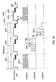
- FIG. 1A is a functional block diagram showing the configuration of a projection apparatus according to a conventional technique
- FIG. 1B is a to view for showing the configuration of a mirror element of the projection apparatus according to a conventional technique
- FIG. 1C is a circuit diagram showing the configuration of the drive circuit of a mirror element of the projection apparatus according to a conventional technique
- FIG. 1D is a timing diagram showing the format of image data used in the projection apparatus according to a conventional technique
- FIG. 1E is a side cross sectional view for illustrating the etendue by exemplifying the case of using a discharge lamp light source and projecting an image by way of an optical device;
- FIG. 2 is a side cross sectional view for showing the relationship among the numerical aperture NA 1 of an illumination light path, the numerical aperture NA 2 of a projection light path and the tilt angle ⁇ of a mirror;
- FIG. 3A is a cross-sectional view of a configuration of a mirror device according to the preferred embodiment 1-1;
- FIG. 3B is a cross-sectional view along line B-B′ (shown in FIG. 3A ) in a configuration example of a mirror element in the mirror device according to the preferred embodiment 1-1;
- FIG. 3C is a cross-sectional view along line A-A′ (shown in FIG. 3A ) in a configuration example of the mirror element in the mirror device according to the preferred embodiment 1-1;
- FIG. 4 shows a side cross sectional view for showing another configuration example of an electrode
- FIG. 5A is a side cross sectional view for showing an example of a deflection state when the mirror is ON;
- FIG. 5B is a side cross sectional view for showing an example of a deflection state when the mirror is OFF;
- FIG. 5C is another side cross sectional view for showing an example of the deflection state when the mirror is OFF;
- FIG. 6 is a block diagram for showing the configuration of a projection apparatus according to a preferred embodiment of the present invention.
- FIG. 7 is a block diagram for showing the configuration of a single-panel projection apparatus according to another preferred embodiment of the present invention.
- FIG. 8A is a block diagram for showing the configuration of a control unit provided to a single-panel projection apparatus according to a preferred embodiment of the present invention.
- FIG. 8B is a block diagram for showing the configuration of a the control unit of a multi-panel projection apparatus according to a preferred embodiment of the present invention.
- FIG. 9A is a block diagram for showing a configuration of a light source drive circuit of a projection apparatus according to a preferred embodiment of the present invention.
- FIG. 9B is a block diagram for showing an alternate configuration of a light source drive circuit of a projection apparatus according to a preferred embodiment of the present invention.
- FIG. 10 is a diagram for showing the relationship between the applied current and the intensity of emission of the light source drive circuit according to a preferred embodiment of the present invention.
- FIG. 11 is a diagram for showing the relationship between the applied current and the intensity of emission of the constant current circuit according to a preferred embodiment of the present invention.
- FIG. 12 is a schematic diagram for showing the layout of the internal configuration of a spatial light modulator according to a preferred embodiment of the present invention.
- FIG. 13 is a cross-sectional view of an individual pixel unit implemented in a spatial light modulator according to a preferred embodiment of the present invention.
- FIG. 14 is a block diagram for showing the configuration of an individual pixel unit implemented in a spatial light modulator according to a preferred embodiment of the present invention.
- FIG. 15 is a timing diagram showing a data configuration of image data used in a preferred embodiment of the present invention.
- FIG. 16A is a timing diagram for illustrating a control signal of a projection apparatus according to the embodiment of the present invention.
- FIG. 16B is a timing for showing a control signal, which is shown by enlarging a part thereof, of a projection apparatus according to the embodiment of the present invention.
- FIG. 17 is a timing diagram for illustrating the control signal of a chirp modulation performed in a projection apparatus according to the embodiment of the present invention.
- FIG. 18 is a timing diagram for illustrating a control signal using binary data performed in a projection apparatus according to the embodiment of the present invention.
- FIG. 19 is another timing diagram for illustrating a control signal using binary data performed in a projection apparatus according to the embodiment of the present invention.
- FIG. 20 is a timing diagram for illustrating a control signal, which is shown by enlarging a part thereof, of a projection apparatus according to the embodiment of the present invention.
- FIG. 21 is a timing diagram for illustrating a control signal of a projection apparatus according to the embodiment of the present invention.
- FIG. 22 is another timing diagram for illustrating a control signal of a projection apparatus according to the embodiment of the present invention.
- FIG. 23 is another timing diagram for illustrating a control signal of a projection apparatus according to the embodiment of the present invention.
- FIG. 24 is another timing diagram for illustrating a control signal of a projection apparatus according to the embodiment of the present invention.
- FIG. 25A is a side cross sectional view of the synthesis optical system of a projection apparatus according to the embodiment of the present invention.
- FIG. 25B is a front view of the synthesis optical system of a projection apparatus according to the embodiment of the present invention.
- FIG. 26 is a block diagram for showing the configuration of a control unit of a projection apparatus according to the embodiment of the present invention.
- FIG. 27 is a timing diagram for illustrating the waveform of a control signal of a projection apparatus according to the embodiment of the present invention.
- the preferred embodiment 1-1 of the present invention relates to a mirror device configured by arranging a plurality of deflectable mirrors as two-dimensional arrays on a substrate and specifically to a method for controlling the deflection angle of a mirror.
- FIG. 1E is cross sectional view for showing the etendue of a light projecting system using a discharge lamp as the light source to project an image through an optical device.
- SLM spatial light modulator
- a spatial light modulator is formed as a two-dimensional array of optical elements, ranging from tens of thousands to millions of miniature modulation elements, with the individual elements enlarged and displayed as the individual pixels corresponding to an image to be displayed onto a screen by way of a projection lens.
- Spatial light modulators generally used for projection apparatuses primarily include two types: 1.) a liquid crystal device, formed by sealing a liquid crystal between transparent substrates, for modulating the polarizing direction of incident light by providing them with a potential, and 2.) a mirror device deflecting miniature micro electro mechanical systems (MEMS) mirrors with electrostatic force and controlling the reflecting direction of illumination light.
- MEMS micro electro mechanical systems
- U.S. Pat. No. 4,662,746 has disclosed an embodiment in which one or two elastic hinges retain a mirror. If the mirror is retained by one elastic hinge, the elastic hinge functions as a bending spring. If the mirror is retained by two elastic hinges, they function as torsion springs to incline the mirror and thereby the reflecting direction of the incident light.
- the on-and-off states of the micromirror control scheme as that implemented in the U.S. Pat. No. 5,214,420 and by most of the conventional display systems impose a limitation on the quality of the display.
- the gray scale PWM between ON and OFF states
- the LSB least significant bit, or the least pulse width
- the least amount of controllable brightness, which determines gray scale, is the light reflected during the least pulse width.
- the limited gray scales lead to degradations of image display.
- FIG. 1C exemplifies a conventional circuit diagram of a control circuit for a micromirror according to U.S. Pat. No. 5,285,407.
- the control circuit includes memory cell 32 .
- Various transistors are referred to as “M*” where * designates a transistor number and each transistor is an insulated gate field effect transistor.
- Transistors M 5 , and M 7 are p-channel transistors; transistors M 6 , M 8 , and M 9 are n-channel transistors.
- the capacitances, C 1 and C 2 represent the capacitive loads of the memory cell 32 .
- Memory cell 32 includes an access switch transistor M 9 and a latch 32 a , which is the basis of the static random access switch memory (SRAM) design.
- SRAM static random access switch memory
- All access transistors M 9 in a row receive a DATA signal from a different bit-line 31 a .
- the particular memory cell 32 is accessed and written by turning on the appropriate row select transistor M 9 , using the ROW signal functioning as a wordline.
- Latch 32 a is formed from two cross-coupled inverters, M 5 /M 6 and M 7 /M 8 , which permit two stable states. State 1 is Node A high and Node B low and state 2 is Node A low and Node B high.
- the mirror driven by a drive electrode abuts a landing electrode is structured differently from the drive electrode, and thereby a prescribed tilt angle is maintained.
- a “landing chip”, which possesses a spring property, is formed on the point of contact between the landing electrode and the mirror. This configuration enhances the deflection of the mirror to the reverse direction upon a change in the control.
- the parts forming the landing chip and the landing electrode are maintained at the same potential so that contact will not cause a shorting or other similar disruption.
- switching between the dual states controls the micromirrors to position either at an ON or an OFF angle, as shown in FIG. 1A .
- the brightness i.e., the gray scales of display for a digitally control image system, is determined by the length of time the micromirror stays at an ON position.
- the length of time a micromirror is controlled at an ON position is in turned controlled by a multiple bit word.
- FIG. 1D shows the “binary time intervals” when controlled by a four-bit word. As shown in FIG.
- the time durations have relative values of 1, 2, 4, 8 that in turn define the relative brightness for each of the four bits, where 1 is for the least significant bit and 8 is for the most significant bit.
- the minimum controllable difference between gray scales is a brightness represented by a “least significant bit” that maintains the micromirror at an ON position.
- the frame time is divided into 2 n ⁇ 1 equal time slices.
- the time slice is 16.7/(2 n ⁇ 1) milliseconds.
- the pixel intensities are determined by the number of time slices represented by each bit. Specifically, a display of a black pixel is represented by 0 time slices. The intensity level represented by the LSB is 1 time slice, and maximum brightness is 2 n ⁇ 1 time slices. The number time slices that a micro mirror is controlled to operate at an On-state in a frame period determines a specifically quantified light intensity of each pixel corresponding to the micromirror reflecting a modulated light to that pixel.
- each pixel corresponding to a modulated micromirror controlled by a control word with a quantified value of more than 0 is operated at an on state for the number of time slices that correspond to the quantified value represented by the control word.
- the viewer's eye integrates the pixels' brightness so that the image appears the same as if it were generated with analog levels of light.
- a pulse width modulator receives the data formatted into “bit-planes”. Each bit-plane corresponds to a bit weight of the intensity value. Thus, if each pixel's intensity is represented by an n-bit value, each frame of data has n bit-planes.
- Each bit-plane has a 0 or 1 value for each display element.
- each bit-plane is separately loaded during a frame.
- the display elements are addressed according to their associated bit-plane values. For example, the bit-plane representing the LSBs of each pixel is displayed for 1 time slice.
- the size of a mirror for constituting such a mirror device is between 4 ⁇ m and 20 ⁇ m on each side.
- the mirrors are placed on a semiconductor wafer substrate in such a manner as to minimize the gap between adjacent mirrors. Smaller gaps reduce random and interfering reflection lights from the gap to prevent such reflections from degrading the contrast of the displayed images.
- the mirror device is formed a substrate that includes an appropriate number of mirror elements. Each mirror element is applied to modulate a corresponding image display element known as a pixel.
- the appropriate number of image display elements is determined according to image display standards in compliance to the resolution of a display specified by the Video Electronics Standards Association (VESA) and to the television-broadcasting standard.
- VESA Video Electronics Standards Association
- the diagonal length of the display area will be about 0.61 inches, thus producing a sufficiently small mirror device
- Projection apparatuses using deflection-type (“deflectable”) light modulators are primarily categorized into two types: 1.) a single-panel projection apparatus comprised of a single spatial light modulator, changing spatially the frequency of a projection light and displaying a color image, and 2.) a multi-panel projection apparatus comprised of a plurality of spatial light modulators, constantly modulating an illumination light with different frequencies by means of the individual spatial light modulators and displaying a color image by synthesizing these modulated lights.
- the single-panel projection apparatus is configured as described above in reference to FIG. 1A .
- NA 1 of an illumination light path there is a close relationship among the numerical aperture (NA) NA 1 of an illumination light path, the numerical aperture NA 2 of a projection light path, and the tilt angle ⁇ of a mirror.
- FIG. 2 shows the relationship among them.
- the illumination light is incident at an angle 2 ⁇ , that is, 24 degrees, relative to the perpendicular axis of the device substrate 1012 .
- the numerical aperture of the projection light path it is desirable for the numerical aperture of the projection light path to be equal to the numerical aperture of the illumination light path. If the numerical aperture of the projection light path is smaller than that of the illumination light path, the illumination light cannot be sufficiently transmitted into the projection light path.
- the numerical aperture of the projection light path is larger than that of the illumination light path, the illumination light can be entirely transmitted (?), but then the projection lens becomes unnecessarily large, which increases the inconvenience in terms of configuring the projection apparatus.
- the light fluxes of the illumination light and projection light must be directed apart from each other because the optical members of the illumination system and those of the projection system must be physically placed in separate locations in an image display system.
- a non-polarizing light source in the emission direction of light such as a high-pressure mercury lamp or xenon lamp, which are generally used for a projection apparatus, its' necessary to maximize the projecting angle of light onto the cross sectional surface of the light path of the illumination light. Since the numerical aperture of the illumination light path is determined by the specification of the tilt angle of the mirror, the tilt angle of the mirror must be increased in order to increase the numerical aperture
- a greater tilt angle of the mirror requires greater space for tilting the mirror that leads to a greater distance between the mirror and an electrode for driving the mirror.
- the drive force is decreased in proportion to the square of the distance d between the electrode and mirror. It is possible to increase the drive voltage in order to compensate for the decrease in the drive force associated with the increase in the distance.
- the drive voltage is about 3 to 15 volts in the drive circuit by means of a CMOS process used for driving a mirror, and therefore, a relatively special process such as a DMOS process is required if a drive voltage in excess of about 15 volts is needed.
- a DMOS process would greatly increase the cost of a mirror device and hence, is undesirable.
- the numerical symbol 4150 denotes the light source
- the numerical symbol 4106 denotes the illumination lens
- the numerical symbol 4107 denotes the device
- the numerical symbol 4108 denotes the projection lens
- the numerical symbol 4109 denotes the projected image.
- the projection lens displays the image on a display surface by enlarging the image modulated with specific resolution and reflected from a spatial light modulator.
- Rp denotes the pixel size of the spatial light modulator
- NA represents the aperture ratio of a projection lens
- F is an F number
- ⁇ is the wavelength of light
- the table below shows the F value of a projection lens and the deflection angle of a mirror by shrinking the mirror size that further shortens the distance between the adjacent mirror elements.
- the F value of a projection lens with the wavelength designated at 700 nm is about 7% smaller than the F value for the wavelength of 650 nm.
- the F numbers of lenses for the illumination system and projection system can be increased to the values shown in the table. Therefore, it is achievable to decrease the deflection angle of the mirror element, and thereby, a smaller mirror device with a low drive voltage can be configured.
- US Patent Application 20050190429 discloses another method for reducing a drive voltage.
- a mirror is held in a free oscillation state in the inherent oscillation frequency, and thereby, the intensity of light that is about 25% to 37% of the emission light intensity when a mirror is controlled under a constant ON state can be obtained during the oscillation period of the mirror.
- the mirror By controlling and operating the mirror with intermediate oscillation state, it is no longer required to drive the mirror in high speed. Furthermore, the intermediate oscillation states enable the projection of images with higher levels of gray scale.
- the mirror also has hinges that have a low spring constant as a spring member for supporting the mirror, and therefore enabling a reduction in the drive voltage. Furthermore, combining this technique with the method of decreasing the drive voltage by decreasing the deflection angle of the mirror, as described above, will increase the level of gray scale to a greater degree.
- the use of a laser light source makes it possible to decrease the deflection angle of a mirror and also shrink the mirror device without decreasing the display brightness. Additionally, by implementing the above-described oscillation control method enables a higher level of gray scale without causing an increase in the drive voltage.
- U.S. Pat. No. 5,583,688, US Patent 20060152690, U.S. Pat. No. 6,198,180, and U.S. Pat. No. 6,992,810 disclose configurations for determining a deflection angle of a mirror in a conventional mirror device.
- the above-disclosed configurations however have difficulties for a person of ordinary skill in the art to increase the size of address electrodes.
- the preferred embodiment 1-1 of the present invention is accordingly configured to integrate the electrode used for driving a mirror element with the stopper used for determining the deflection angle of a mirror.
- FIG. 3A is a top view of a mirror for illustrating the configuration of the mirror element of a mirror device according to the preferred embodiment 1-1.
- FIG. 3B is a side cross-sectional view for showing the configuration of the mirror element of the mirror device according to the preferred embodiment 1-1.
- FIG. 3C is another side cross-sectional view for showing the configuration of the mirror element of the mirror device according to the preferred embodiment of 1-1.
- FIGS. 3A to 3C show a mirror element that includes a mirror 1101 having a highly reflective top surface coated with material, such as aluminum or gold.
- the mirror 1101 is supported by an elastic hinge 1102 made of a silicon material, a metallic material and the like, and is placed on a substrate 1103 .
- the silicon material may include poly-silicon, single crystal silicon and amorphous silicon
- the metallic material may include aluminum, titanium, and an alloy of some of these metallic materials, or a composite of these metals or alloys.
- the mirror 1101 is in the approximate shape of a square, with the length of one side, for example, between 4 ⁇ m and 11 ⁇ m.
- the size of adjacent mirrors is also between, for example, 4 ⁇ m and 11 ⁇ m.
- the deflection axis 1111 of the mirror 1101 is on the diagonal line.
- the lower end of the elastic hinge 1102 is connected to the substrate member 1103 that includes a circuit for driving the mirror 1101 .
- the upper end of the elastic hinge 1102 is connected to the bottom surface of the mirror 1101 .
- An electrode for reliably maintain electrical connectivity and an intermediate member for strengthening the support structures and strengthening the connection may be placed between the elastic hinge 1102 and substrate 103 , or between the elastic hinge 1102 and mirror 1101 .
- electrodes 1104 used for driving the mirror 1101 are placed on the top surface of the substrate 1103 , opposite the bottom surface of the mirror 1101 .
- the form of the electrode 1104 may be symmetrical or asymmetrical about the deflection axis 1111 .
- the electrode 1104 is made of aluminum or tungsten.
- the present embodiment is configured such that the electrode 1104 also carries out the function of a stopper for contacting and stopping the mirror from further movement when the mirror is deflected to a maximum deflection angle.
- deflection angle of the mirror 1101 may be controlled to operate between 10 degrees and 14 degrees relative to the horizontal state of the mirror 1101 or between 2 degrees and 10 degrees relative to the horizontal state of the mirror 1101 .
- Configuring the electrode 1104 to also function as stopper makes it possible to maximize the electrode layout space when shrinking the mirror element, as compared to the conventional method of placing the electrode and stopper individually,.
- the electrode may be formed, as shown in FIGS. 3A through 3C , as a trapezoid, with the top and bottom sides approximately parallel to the deflection axis 1111 , and the sloped sides approximately parallel to the contour line of the mirror 1101 of the mirror device.
- the deflection axis of the mirror 1101 is matched with the diagonal line of the electrode.
- the electrode and stopper can usually be simultaneously manufactured as in the conventional method, and therefore such the electrode and stopper may be conveniently formed during the manufacturing processes.
- the present embodiment using the electrode also as stopper is configured to provide the surface of the electrode and/or the rear surface of the mirror with an insulation layer(s) in order to prevent an electrical shorting at point of contact between the mirror and the electrode. If the surface of the electrode is coated with an insulation layer, the configuration may be such that the insulation layer covers only a part of the electrode, including the portion coming in contact with the mirror.
- FIGS. 3A through 3C exemplify the case of covering the surface of the electrode 1104 (i.e., 1104 a and 1104 b ) with an insulation layer 1105 (i.e., 1105 a and 1105 b ).
- the insulation layer is made of oxidized compounds, azotized compounds, silicon or silicon compounds, e.g., SiC, SiO 2 , Al 2 O 3 , and Si.
- the material and thickness of the insulation layer is determined so that the dielectric strength voltage is maintained at no less than the voltage required to drive the mirror, preferably no less than 5 volts.
- the dielectric strength voltage may be configured to be two times the drive voltage of the mirror or higher, 3 volts or higher or 10 volts or higher.
- FIG. 4 for side cross sectional view of a mirror, where “L 1 ” is the distance between the deflection axis and the edge of the electrode on a side closer to the deflection axis of the mirror 1101 .
- the distance shown by “L 2 ” is the distance between the deflection axis and the edge of the electrode on a side farther from the deflection axis of the mirror 1101
- “d 1 ” and “d 2 ” are the distances between the mirror's bottom surface and the top of the electrode at its respective edges.
- P 1 is a representative point on the electrode's edge on the side closer to the deflection axis of the mirror
- P 2 is a representative point on the electrode's edge on the side farther from the deflection axis of the mirror.
- the mirror shown in FIG. 4 is the case in which the electrode is formed so that d 1 ⁇ d 2 .
- the stopper determining the tilt angle of the mirror 1101 is preferably placed at the point P 2 in consideration of a production variance of the electrode height that influences the deflection angle of the mirror.
- the present embodiment is accordingly configured to satisfy the relationship of: d 1>( L 1* d 2)/ L 2
- FIGS. 5A to 5C for showing the light reflection from the mirrors.
- the mirror configuration and operation of mirror deflections present different deflection states when different voltages are applied to the electrodes.
- the light incident to the mirror 1212 is deflected in a specific direction as shown in FIGS. 5A through 5C .
- LSB least significant bit
- the changeover transition time t M of a mirror is approximately equal to the natural oscillation frequency of the oscillation system of the mirror. Accordingly, the LSB is required to control the mirror that the light intensity in the interim during the changeover transition can be ignored.
- the gray scale reproducible with the above-described hinge is about 8-bit, even if the LSB is set at five times the changeover transition time t M . Therefore, compared with a conventional display system, the display systems of this invention can achieve an image display with a 10-bit grayscale by using the 8-bit grayscale control signals because of the implementation of the intermediate control states.
- the present embodiment is configured to set the mirror to oscillate with a natural oscillation cycle of the oscillation system.
- the display system includes an elastic hinge.
- the natural oscillation cycle can be set between about 1.8 ⁇ sec and 108.5 ⁇ sec with three deflection states.
- the mirror element in a first deflection state is modulated by the mirror element directed towards the projection light path.
- the mirror element in the second deflection state is controlled to reflect a light in a direction away from the projection light path.
- the mirror element in a third deflection state is controlled to oscillate between the first and second deflection states.
- the intermediate state provide a reduced amount of controllable light thus enabling the display system to display images of a gray scale with higher resolution without increasing the drive voltage of the mirror element.
- the present embodiment is configured to make the electrode also function as a stopper for regulating the maximum deflection angle of the mirror.
- the electrode By configuring the electrode to sever also as a stopper increases the efficiency of space usage while shrinking the mirror element and expanding the area of the electrode.
- FIG. 6 is a functional block diagram for showing the configuration of a projection apparatus according to a preferred embodiment of the present invention.
- FIG. 6 shows a projection apparatus 5010 according to the present embodiment comprises a single spatial light modulator (SLM) 5100 , a control unit 5500 , a Total Internal Reflection (TIR) prism 5300 , a projection optical system 5400 and a light source optical system 5200 .
- SLM spatial light modulator
- TIR Total Internal Reflection
- the projection apparatus 5010 is commonly referred to as a single-panel projection apparatus 5010 that includes a single spatial light modulator 5100 .
- the projection optical system 5400 includes a spatial light modulator 5100 and a TIR prism 5300 disposed along the optical axis of the projection optical system 5400 , and the light source optical system 5200 is disposed for projecting a light along the optical axis matches with the optical path of the projection optical system 5400 .
- the TIR prism 5300 receives the incoming illumination light 5600 projects from the light source optical system 5200 and directs the light to transmit as incident light 5601 to the spatial light modulator 5100 at a prescribed inclination angle.
- the SLM 5100 further reflects and transmits a the reflection light 5602 , towards the projection optical system 5400 .
- the projection optical system 5400 receives the light 5602 reflected from the SLM 5100 onto a screen 5900 as projection light 5603 .
- the light source optical system 5200 comprises a variable light source 5210 for generating the illumination light 5600 , a condenser lens 5220 for focusing the illumination light 5600 , a rod type condenser body 5230 and a condenser lens 5240 .
- variable light source 5210 , condenser lens 5220 , rod type condenser body 5230 and condenser lens 5240 are sequentially placed in the aforementioned order along the optical axis of the illumination light 5600 emitted from the variable light source 5210 and incident to the side face of the TIR prism 5300 .
- the projection apparatus 5010 employs a single spatial light modulator 5100 for projecting a color display on the screen 5900 by applying a sequential color display method.
- the variable light source 5210 comprises a red laser light source 5211 , a green laser light source 5212 and a blue laser light source 5213 (not specifically shown here).
- the variable light source allows independent controls for the light emission states.
- the controller of the variable light source performs an operation of dividing one frame of display data into a plurality of sub-fields (i.e., three sub-fields, that is, red (R), green (G) and blue (B) in the present case) and turns on each of the red laser light source 5211 , green laser light source 5212 and blue laser light source 5213 to emit each respective light in time series at the time band corresponding to the sub-field of each color as will be described later.
- the light sources are laser light sources.
- the light sources may also be semiconductor light sources such as the light emitting diodes (LEDs).
- FIG. 7 is a functional block diagram for showing the configuration of a projection apparatus according to an alternate preferred embodiment of the present invention.
- the projection apparatus 5020 is commonly referred to as a multiple-plate projection apparatus that includes a plurality of spatial light modulators 5100 instead of a single SLM included in the single-panel projection apparatus 5010 described earlier. Further, the projection apparatus 5020 comprises a control unit 5502 in place of the control unit 5500 .
- the projection apparatus 5020 comprises a plurality of spatial light modulators 5100 , and further includes a light separation/synthesis optical system 5310 between the projection optical system 5400 and each of the spatial light modulators 5100 .
- the light separation/synthesis optical system 5310 comprises a plurality of TIR prisms, i.e., a TIR prism 5311 , a prism 5312 , and a prism 5313 .
- the TIR prism 5311 carries out the function of directing the illumination light 5600 projected along the optical axis of the projection optical system 5400 and directs the light to the spatial light modulator 5100 as incident light 5601 .
- the TIR prism 5312 carries out the function of separating red (R) light from an incident light 5601 , projected by way of the TIR prism 5311 , to transmit the red light to the spatial light modulators for the red light 5100 , and further carries out the function of directing the reflection light 5602 of the red light to the TIR prism 5311 .
- the prism 5313 carries out the functions of separating blue (B) and green (G) lights from the incident light 5601 projected by way of the TIR prism 5311 , and directs the light to the blue color-use spatial light modulators 5100 and green color-use spatial light modulators 5100 , and further carries out the function of directing the reflection light 5602 of the green light and blue light to the TIR prism 5311 .
- the spatial light modulations of these three colors, R, G and B carry out these functions simultaneously by these three spatial light modulators 5100 .
- the reflection light 5602 resulting from the respective modulations, is projected onto the screen 5900 as the projection light 5603 by way of the projection optical system 5400 , and thus a color display is carried out.
- system may implement various modifications by using a light separation/synthesis optical system instead of the light separation/synthesis optical system 5310 described above.
- FIG. 8A is a functional block diagram for showing a configuration of the control unit 5500 implemented in the above described single-panel projection apparatus 5010 .
- the control unit 5500 comprises a frame memory 5520 , an SLM controller 5530 , a sequencer 5540 , a light source control unit 5560 and a light source drive circuit 5570 .
- the sequencer 5540 includes a microprocessor to control the operation timing of the entire control unit 5500 and the spatial light modulators 5100 .
- the frame memory 5520 retains one frame of input digital video data 5700 received from an external device (not shown in the figure) connected to a video signal input unit 5510 .
- the input digital video data 5700 is updated in real time whenever the display of one frame is completed.
- the SLM controller 5530 processes the input digital video data 5700 read from the frame memory 5520 as described later.
- the SLM controller separates the data read from the memory 5520 into a plurality of sub-fields according to detail descriptions further describe below.
- the SLM controller outputs the data subdivided into subfields to the spatial light modulators 5100 as binary data 5704 and non-binary data 5705 , which are used for implementing an the ON/OFF control and oscillation control (which are described later) of a mirror 5112 of the spatial light modulator 5100 .
- the sequencer 5540 outputs a timing signal to the spatial light modulators 5100 in sync with the generation of the binary data 5704 and non-binary data 5705 at the SLM controller 5530 .
- the video image analysis unit 5550 outputs a image analysis signal 5800 used for generating various light source pulse patterns (which are described later) corresponding to the input digital video data 5700 inputted from the video signal input unit 5510 .
- the light source control unit 5560 controls the light source drive circuit 5570 to control the operation of the variable light source 5210 by using a light source profile control signal in emitting the illumination light 5600
- the light source profile control signal is generated from the image analysis signal 5800 on the basis of the input of the image analysis signal 5800 generated by the video image analysis unit 5550 using data of the light source pulse patterns generated by the sequencer 5540 as will be further described below.
- the light source drive circuit 5570 performs the operation of driving the red laser light source 5211 , green laser light source 5212 and blue laser light source 5213 of the variable light source 5210 to emit light, respectively.
- the light source generates the light source pulse patterns 5801 through 5811 (which are described later) received from the light source control unit 5560 .
- FIG. 8B is a functional block diagram for illustrating the configuration of the control unit of a multi-panel projection apparatus according to the present embodiment.
- the control unit 5502 comprises a plurality of SLM controllers 5531 , 5532 and 5533 , which are used for controlling each of the spatial light modulators 5100 .
- Each of these modulators is implemented for modulating the respective colors R, G and B, and the configuration of the controllers is the main difference between the control unit 5502 and the control unit 5500 described in FIG. 8A .
- each of the SLM controller 5531 , SLM controller 5532 and SLM controller 5533 is implemented to process the modulation of a respective colors Red, Green, and Blue.
- Each modulator is supported on the same substrates as those of the respective spatial light modulators 5100 . This configuration makes it possible to place the individual spatial light modulators 5100 and the corresponding SLM controller 5531 , SLM controller 5532 and SLM controller 5533 close to each other, thereby enabling a high speed data transfer rate.
- a system bus 5580 is used to connect the frame memory 5520 , light source control unit 5560 , sequencer 5540 and SLM controllers 5531 through 5533 , in order to speed up and simplify the connection path of each connecting element.
- FIG. 9A is a block diagram for showing the configuration of the light source drive circuit 5570 (i.e., the light source drive circuits 5571 , 5572 and 5573 ) according to the present embodiment.
- the light source drive circuit shown in FIG. 9A includes a plurality of constant current circuits 5570 a (i.e., I (R, G, B) 1 through I (R, G, B) n ) and a plurality of switching circuits 5570 b (i.e., switching circuits SW (R, G, B) 1 through SW (R, G, B) n ) corresponding to the respective constant current circuits 5570 a , in order to generates the desired light intensities.
- the light emission are shown as P 1 through P n for the light source optical system 5200 (i.e., the red laser light source 5211 , green laser light source 5212 and blue laser light source 5213 ).
- the switching circuit 5570 b carries out a switching in accordance with a desired emission profile of the light source optical system 5200 (i.e., the red laser light source 5211 , green laser light source 5212 and blue laser light source 5213 ).
- the setup values of the output current of the constant current circuits 5570 a i.e., constant current circuits I (R, G, B) n ), when the gray scale of the emission intensity of the light source optical system 5200 is designated at N bits (where N ⁇ n), are as follows:
- a gray scale display controlled on the basis of the emission intensity.
- a similar gray scale display is achievable even if the emission period (i.e., an emission pulse width) and the emission interval (i.e., an emission cycle) are variable.
- FIG. 9B is a block diagram for showing a modified embodiment of the configuration of the light source drive circuit according to the present embodiment.
- FIG. 9B denotes the constant current circuits 5570 a (I (R, G, B) 1 through I (R, G, B) n ) as I I through I n and the switching circuits 5570 b (SW (R, G B) 1 through SW (R, G, B) n ) as switching circuits 5570 b (SW 1 through SW n ).
- the light source drive circuits 5570 is configured to control the individual constant current circuit 5570 a (i.e., I (R, G, B) 1 in this case) to supply a current equivalent to the threshold current I th of the light source optical system 5200 .
- the individual constant current circuit supplies a current close to the aforementioned threshold current, as a bias current I b when a semiconductor laser or a similar light source is used as the light source optical system 5200 .
- the respective switching operation of the light source drive circuits 5570 is stabilized to provide a high-speed emission.
- the light source drive circuits 5570 (i.e., the light source drive circuits 5571 , 5572 , and 5573 ) shown in FIG. 9B comprises bias current circuits 5570 c , which are continuously connected to the light source optical systems 5200 (i.e., the red laser light source 5211 , green laser light source 5212 and blue laser light source 5213 ) and which are used for applying a bias current I b , in addition to the constant current circuits 5570 a.
- connection of the constant current circuits 5570 a to the light source optical systems 5200 is configured through a switching circuit 5570 d (SW pulse ) that includes on the downstream side of the switching circuits 5570 b.
- SW pulse switching circuit 5570 d
- the relationship between the emission intensity P n and drive current of the variable light source for each wavelength is as follows, where “k” is the emission efficiency in terms of drive current:
- FIG. 9B shows an embodiment wherein the switching circuits 5570 d can carries out a circuit operation unaffected by a drive current switching over that may be caused by the switching circuits 5570 b (SW 1 through SW n ).
- Each of the switching circuits 5570 b is connected to the respective constant current circuits 5570 a .
- a further function is carried out that when the variable light source 5210 is not emitting light, the above-described switching circuits (SW 1 through SW n ) are switched over.
- bias current value is designated at a fixed current value in the configuration of FIG. 9B , it is also possible to connect the bias current circuit 5570 c to the light source control unit 5560 and allows a variable bias current.
- FIG. 10 is a diagram for showing the relationship between the applied current I and emission intensity P n of the constant current circuit 5570 a of the light source drive circuit shown in the above described FIG. 9A .
- FIG. 11 is a diagram for showing the relationship between the applied current I and emission intensity P n of the constant current circuit 5570 a of the light source drive circuit shown in the above described FIG. 9B .
- FIGS. 9A and 9B have been provided for the case of changing the emission profiles of the variable light source for each sub-frame corresponding to each gray scale bit. If the display gray scale function of the spatial light modulator 5100 is used in parallel, the number of required levels of electrical current decreases, thus reducing the number of constant current circuits 5570 a and also the number of the switching circuits 5570 b . It is therefore possible to obtain the number of gray scales equal to, or higher than, the gray scales achievable through the modulation process of the spatial light modulator 5100 .
- the spatial light modulator 5100 is a deflectable mirror device that arranges a plurality of mirror elements in two-dimensional array.
- FIG. 12 is a circuit schematic diagram for illustrating the layout of the internal configuration of the spatial light modulator 5100 according to the present embodiment.
- FIG. 13 is a cross-sectional diagram of an individual pixel unit constituting the spatial light modulator 5100 according to the present embodiment.
- FIG. 14 is a side cross sectional view for showing the configuration of an individual pixel unit implemented in the spatial light modulator 5100 according to the present embodiment.
- FIG. 12 shows an exemplary embodiment of a spatial light modulator 5100 that includes a mirror element array 5110 , column drivers 5120 , ROW line decoders 5130 and an external interface unit 5140 .
- the external interface unit 5140 comprises a timing controller 5141 and a selector 5142 .
- the timing controller 5141 controls the ROW line decoder 5130 on the basis of a timing signal from the SLM controller 5530 .
- the selector 5142 supplies the column driver 5120 with digital signal incoming from the SLM controller 5530 .
- mirror element array 5110 a plurality of mirror elements are arrayed at the positions where individual bit lines 5121 vertically extended from the column drivers 5120 , crosses over the individual word lines 5131 horizontally extended from the ROW line decoders 5130 .
- the individual mirror element 5111 that includes a freely deflectable mirror 5112 supported on a substrate 5114 by way of a hinge 5113 .
- the mirror 5112 is covered with a cover glass 5150 for protection.
- the mirror further includes an OFF electrode 5116 (and an OFF stopper 5116 a ) and an ON electrode 5115 (and an ON stopper 5115 a ).
- the electrodes and stoppers are symmetrically placed across the hinge 5113 on the substrate 5114 .
- the OFF electrode 5116 attracts the mirror 5112 with a coulomb force by the application of a predetermined voltage and tilts the mirror 5112 to a position of contact with the OFF stopper 5116 a . This causes the incident light 5601 incident to the mirror 5112 to reflect in a light path along an OFF direction away from the optical axis of the projection optical system 5400 .
- the ON electrode 5115 draws the mirror 5112 with a coulomb force by applying a predetermined voltage and tilts the mirror 5112 to a position of contact with the ON stopper 5115 a . This causes the incident light 5601 incident to the mirror 5112 reflect in a light path along the ON direction to align with the optical axis of the projection optical system 5400 .
- the single-panel projection apparatus 5010 (1 ⁇ SLM); comprising a single SLM receiving one frame of input digital video data 5700 shown as a frame 6700 - 1 in FIG. 15 .
- the frame 6700 - 1 in includes a plurality of sub-frames 6701 , 6702 and 6703 in a time series corresponding to the respective colors R, G and B.
- the binary data 6704 or non-binary data 6705 , is generated for each subfield as described above.
- a multi-panel projection apparatus 5020 comprising three SLMs receives a control data that includes a plurality of subfields 6700 - 2 , i.e., equivalent to subfields 6701 , 6702 and 6703 ) corresponding to the respective colors R, G and B output simultaneously and in parallel to the respective spatial light modulators 5100 .
- the spatial light modulation for the respective colors are carried out simultaneously and in parallel during the display period of one frame (i.e., a frame 6700 - 1 ), as exemplified in the bottom half of FIG. 15 .
- above-described binary data 6704 or non-binary data 6705 is generated for each subfield 6700 - 2 of each respective color.
- the present embodiment is configured such that the video image analysis unit 5550 of the control unit 5500 detects, from the input digital video data 5700 , the timing of a change of the signal waveforms of the binary data 6704 or non-binary data 6705 .
- the control unit 5500 generates a light source profile control signal 6800 for controlling the ON/OFF of the red laser light source 5211 , green laser light source 5212 and blue laser light source 5213 of the variable light source 5210 , and inputs the signal to the light source control unit 5560 by way of the sequencer 5540 .
- This configuration implements the ON/OFF control (which is described later) of the variable light source 5210 in sync with the timing of a change in the signal waveforms of the binary data 6704 or non-binary data 6705 of the input digital video data 5700 .
- the embodiment shown in FIG. 8A makes it possible to continuously adjust the intensity of emission of the variable light source 5210 while the spatial light modulator 5100 is driven. That is, the embodiment makes it possible to change the brightness of a pixel during the display of an image onto the screen 5900 , thereby enabling a control of the gray scale characteristic of the display video image. Further, the present embodiment is configured to adjust the emission intensity of the variable light source 5210 using a drive signal used for driving the spatial light modulator 5100 , eliminating extraneous emissions from the variable light source 5210 , reducing both the heat emitted and the power consumed.
- FIG. 16A illustrates an example of the waveform of a mirror control profile 6720 that is a control signal generated from a SLM controller 5530 to a spatial light modulator 5100 .
- FIG. 16A further shows an exemplary waveform of a light source pulse pattern 6801 generated by a light source control unit 5560 from a light source profile control signal 5800 , corresponding to the aforementioned mirror control profile 6720 .
- one frame of the mirror control profile 6720 includes the combination of a mirror ON/OFF control 6721 on the beginning portion of a frame and a mirror oscillation control 6722 near the end portion of the frame period used for controlling the tilting operation of the mirror 5112 corresponding to the gray scale of the present frame.
- the mirror ON/OFF control 6721 controls the mirror 5112 in either of the ON and OFF states
- the mirror oscillation control 6722 controls the mirror 5112 in an oscillation state, in which the mirror 5112 oscillates between the ON state and the OFF state.
- the present embodiment is configured such that the light source control unit 5560 controls the frequencies of the pulse emission of the variable light source 5210 in accordance with the signal (i.e., mirror control profile 6720 ) driving the spatial light modulator 5100 .
- the spatial light modulator 5100 performs a modulation of the illumination light 5600 through a spatial light modulation process with the SLM includes a large number of mirrors 5112 corresponding to the pixels to be displayed and the tilting operation of the mirrors 5112 .
- the mirror oscillation control 6722 , the pulse emission frequency fp of the variable light source 5210 emitting the illumination light 5600 is preferably either higher (in the case of the light source pulse pattern 6801 shown in FIG. 16A ) by ten times, or more, than the oscillation frequency fp of the oscillation control for the mirror 5112 , or lower (in the case of the light source pulse pattern 6802 shown in FIG. 16A ) by one tenth, or less, than the frequency fm.
- FIG. 16B is a timing diagram for showing the above described light source pulse pattern 6801 .
- the top portion shows an expanded waveform corresponding to the mirror oscillation control 6722 .
- the mirror oscillation control 6722 oscillates at an oscillation cycle t osc (1/fm) and, in contrast the light source pulse pattern 6801 , performs pulse emission at a pulse emission frequency fp (1/(tp+ti)) with [emission pulse width tp+emission pulse interval ti] as one cycle.
- the condition is: fp>(fm*10)
- the present embodiment is configured to change the frequencies of the pulse emission of the variable light source 5210 , thereby making it possible to adjust the intensity of the illumination light 5600 emitted
- FIG. 17 shows a light source pulse pattern 6803 to carry out a chirp modulation, in which the pulse emission frequencies fp of the variable light source 5210 are continuously changed from a high frequency to a low frequency while the spatial light modulator 5100 is driven.
- the continuous changing of the pulse emission frequencies fp as exemplified by the light source pulse pattern 6803 makes it possible to extend the number gray scales in the darker parts of an image and thereby allowing the details in the darker part of an image to be displayed without saturating the brighter parts of an image.
- FIG. 18 shows a mirror control profile 6710 controls and drives the spatial light modulator 5100 .
- the mirror control profile 6710 includes binary data 6704 generated by the SLM controller 5530 .
- the pulse emission frequencies fp of the variable light source 5210 are changed during a period corresponding to the LSB of the binary data 6704 .
- FIG. 18 shows the reduction of the pulse emission frequency fp by increasing an emission pulse interval ti, while keeping the emission pulse width tp fixed in the section of the LSB.
- the configuration makes it possible to adjust the light intensity of the light source by changing the pulse emission frequencies fp of the variable light source 5210 in the LSB period.
- By adjusting the intensity of the light source in the minimum period for driving the mirror 5112 increases the number of bits for controlling the gray scale of the image display.
- FIG. 19 is a timing diagram for showing a light source pulse pattern 6805 .
- the spatial light modulator 5100 is driven with a mirror control profile 6710 that includes binary data 6704 generated by the SLM controller 5530 . Furthermore, the pulse emission frequency fp of the variable light source 5210 is changed to half during the period of the LSB of the mirror control profile 6710 .
- the pulse emission frequency fp of the light source pulse pattern 6805 is reduced to half with a time of the LSB period for controlling the mirror control profile 6710 .
- the light intensity of the variable light source 5210 is reduce to 50% and that makes it possible to increase the drive time of the mirror 5112 to two times the LSB period.
- the use of common light source intensity achieves the same light intensity of the illumination light 5600 as the light intensity obtained during the LSB period.
- the period of drive time of the mirror 5112 can be increased to two times the LSB period, and therefore, the control of the spatial light modulator 5100 can be simplified.
- FIG. 20 is a timing diagram for showing the operation of changing the emission pulse widths tp of the pulse emission of the variable light source 5210 in accord with a signal driving the spatial light modulator 5100 .
- the emission pulse width tp is increased as the light source pulse pattern 6806 , or alternately decreased as the light source pulse pattern 6807 , depending on the mirror control profile 6720 including the mirror ON/OFF control 5721 and mirror control profile 6720 .
- the present embodiment is implemented by changing the emission pulse widths tp of the pulse emission of the variable light source 5210 .
- the pulse emission frequency fp is kept at constant, thereby making it possible to adjust the emission intensity of the illumination light 5600 , such as a laser light, emitted from the variable light source 5210 .
- FIG. 21 is a timing diagram for showing the change of the emission light intensities of the emission pulse of the variable light source 5210 in accordance with a mirror control profile 6720 driving the spatial light modulator 5100 .
- the light source pulse pattern 6808 controls, in sync with the mirror control profile 6720 , the emission intensity by using the emission pulse width tp, emission pulse interval ti and emission intensity Ph 1 .
- the light source pulse pattern 6809 controls, in sync with the mirror control profile 6720 , the emission intensity by using an emission intensity Ph 2 ( ⁇ emission intensity Ph 1 ) with the emission pulse width tp and emission pulse interval ti held constant.
- the present embodiment is configured to change the emission light intensities of the emission pulse, thereby making it possible to adjust the emission intensity of the variable light source 5210 , such as a laser.
- FIG. 22 is a timing diagram for showing the case of changing the emission light intensities using any one of the following parameters: the pulse emission frequency, emission pulse width, emission intensity of a pulse, or a discretionary combination of multiple parameters from among the aforementioned parameters so as to correspond to the mirror control profile 6720 driving the spatial light modulator 5100 .
- the light source pulse pattern 6810 shown in FIG. 22 illustrates the case of changing the pulse emission frequency fp, emission pulse width tp, emission intensity Ph 3 and emission intensity Ph 4 , in sync with the mirror control profile 6720 .
- the light source pulse pattern 6810 performs a control such that, in the display period of one frame, first, the pulse emission frequency fp is gradually increased while the emission intensity Ph 3 and emission pulse width tp are kept constant and then, in the latter part of the frame, the emission pulse width tp is increased of the section of mirror ON/OFF control 6721 .
- the emission intensity is increased to the emission intensity Ph 4 (which is larger than the emission intensity Ph 3 ) and the emission pulse width tp is also increased to a value that is equal to the width of the oscillating section 6722 .
- Controlling the light source pulse pattern 6810 makes it possible to expand the gray scales in, for example, a darker part of a video image, enabling a display of details in a darker part of the image without saturating the brighter parts of the video image.
- the present embodiment enables control of the gray scale of a displayed image, by changing the parameters of the pulse emission of the variable light source 5210 , such as pulse emission frequency fp, emission pulse width tp, and emission light intensities Ph 3 and Ph 4 .
- FIG. 23 is another timing diagram for showing the application of the control data for making a variable light source 5210 emit pulses only during the period in which the entire pixels of a spatial light modulator 5100 are driven and suppressing the pulse emission of the variable light source 5210 during the period in which the entire pixels of the spatial light modulator 5100 are not driven.
- the light source pulse pattern 6811 shown in FIG. 23 is generated in sync with the mirror control profile 6720 , which makes the variable light source 5210 perform pulse emission during the period of driving the mirror 5112 by means of the mirror control profile 6720 and suppressing the pulse emission during the turn-off period t off between frames.
- the present embodiment is implemented with the variable light source 5210 emitting light only when the spatial light modulator 5100 is driven. Therefore the power consumption of the projection apparatus and the heat generation of the variable light source 5210 can be reduced.
- FIG. 24 is a timing diagram for showing the application of the control data for projecting a color display by means of a color sequential control using the control unit 5505 , which is exemplified in FIG. 8A , on a single-panel projection apparatus comprising one spatial light modulator 5100 as exemplified in the above described FIG. 6 .
- the display period of one frame (i.e., frame 6700 - 1 ) is further divided, in a time series, to the subfields 6701 , 6702 and 6703 , corresponding to the respective colors G, R and B.
- the pulse emission of the green laser light source 5212 is controlled in accordance with a light source pulse pattern 6812 in the green (G) subfield 6701 ; the pulse emission of the red laser light source 5211 is controlled in accordance with a light source pulse pattern 6813 in the red (R) subfield 6702 ; and the pulse emission of the blue laser light source 5213 is controlled in accordance with a light source pulse pattern 6804 .
- the light source drive circuit 5570 performs a control in order to adjust the emission light intensities for the red laser light source 5211 , green laser light source 5212 and blue laser light source 5213 of the respective colors R, G and B in accordance with the mirror control profile 6720 generated by the SLM controller 5530 .
- the present embodiment makes it possible to expand the gray scale of the respective colors R, G and B in a color display on a color sequential projection apparatus.
- FIGS. 25A and 25B are functional block diagrams which, taken together, show the configuration of the optical system of a projection apparatus comprising a plurality of spatial light modulators 5100 .
- FIG. 25A is a side view of a synthesis optical system according to the present embodiment
- FIG. 25B is the front view diagram.
- the optical system comprises a device package 5100 A, which integrates a plurality of spatial light modulators 5100 , a color synthesis optical system 5340 , a light source optical system 5200 , and a variable light source 5210 .
- the plurality of spatial light modulators 5100 incorporated in the device package 5100 A is fixed in a position in which the rectangular contour of the spatial light modulator 5100 is inclined at approximately 45 degrees, on a horizontal plane, relative to each side of the device package 5100 A, which has a similarly contoured rectangular shape.
- the color synthesis optical system 5340 is placed on the device package 5100 A.
- the color synthesis optical system 5340 is comprised of right-angle triangle pole-shaped prisms 5341 and 5342 , which are joined together to form an equilateral triangle column on the longitudinal side, and a right-angle triangle column-shaped light guide block 5343 .
- a sloped surface of the light guide block 5343 is attached, with adhesives, to the side faces of prisms 5341 and 5342 , with the bottom surface of the light guide block 5343 facing up.
- a light absorption body 5344 is placed on the surface of the side opposite to the side on which the light guide block 5343 is adhesively attached.
- the bottom of the light guide block 5343 is equipped with the light source optical system 5200 of the green laser light source 5212 , and the light source optical system 5200 of the red laser light source 5211 and blue laser light source 5213 , with the optical axis of each of the light source optical systems 5200 maintained in a vertical position.
- the illumination light 5600 emitted from the green laser light source 5212 is incident to the spatial light modulator 5100 , on one side, which is positioned immediately under the prism 5341 , as incident light 5601 , by way of the light guide block 5343 and the present (??) prism 5341 .
- the illumination lights 5600 respectively emitted from the red laser light source 5211 and the blue laser light source 5213 are incident to the spatial light modulator 5100 , on the other side, which is positioned immediately under the prism 5342 , as the incident light 5601 , by way of the light guide block 5343 and the prism 5342 .
- the green incident light 5601 incident to the spatial light modulator 5100 , is reflected in the vertically upward direction as a reflection light 5602 in the prism 5341 , is further reflected by the external surface of the prism 5341 , follows the same light path as the red and blue reflection lights 5602 , and is incident to the projection optical system 5400 , in which the incident light becomes the projection light 5603 , in the ON state of the mirror 5112 .
- the mirror device is configured to accommodate at least two modules of spatial light modulators 5100 in a single device package 5100 A.
- One module is illuminated only with the incident light 5601 from the green laser light source 5212 .
- the other module of the spatial light modulator 5100 is illuminated with the incident light 5601 from either or both of the red laser light source 5211 or blue laser light source 5213 .
- Individual modulation lights respectively modulated by two spatial light modulators 5100 are collected at the color synthesis optical system 5340 as described above. The collected light is further expanded by the projection optical system 5400 and projected onto the screen 5900 , or the like, as the projection light 5603 .
- FIG. 26 is a block diagram for showing the configuration of a control unit 5506 situated in the projection apparatus, configured as exemplified in the above described FIGS. 25A and 25B .
- FIG. 27 is a timing diagram for showing the waveform of a control signal of the projection apparatus, according to the present embodiment 3-8.
- a drive signal (i.e., the mirror control profile 6720 shown in FIG. 27 ) generated by the SLM controller 5530 drives the plurality of spatial light modulators 5100 packaged in the device package 5100 A.
- the light source control unit 5560 generates a light source profile control signal 5800 corresponding to the mirror control profile 6720 that is the signal driving the respective spatial light modulators 5100 and inputs the generated profile 6720 into the light source drive circuit 5570 , which in turn adjusts the intensity of the laser lights (i.e., the illumination lights 5600 ) emitted, respectively, from the red laser light source 5211 , green laser light source 5212 and blue laser light source 5213 .
- the control unit 5506 of the projection apparatus according to the present embodiment 3-8 is configured such that one SLM controller 5530 drives a plurality of spatial light modulators 5100 .
- the illumination lights 5600 is provided to project lights to the respective spatial light modulators 5100 with the most optimal intensity without requiring the individual spatial light modulators 5100 to include a light source control unit 5560 or light source drive circuit 5570 .
- This configuration simplifies the circuit configuration of the control unit 5506 .
- FIG. 27 is a timing diagram for showing the control signals of the light source control unit 5560 and light source drive circuit 5570 drive the red laser light source 5211 , green laser light source 5212 and blue laser light source 5213 so as to adjust the emission intensities of the individual lasers (i.e., the illumination light 5600 ) of the respective colors R, G and B in sync with the respective SLM drive signal (i.e., the mirror control profile 6720 ) that are generated by the SLM controller 5530 .
- the respective SLM drive signal i.e., the mirror control profile 6720
- a color sequence control is employed for modulating and displaying the two colors B and R sharing one spatial light modulator 5100 .
- One frame includes a plurality of subfields 6701 , 6702 and 6703 , and the same light source pulse pattern 6815 is repeated in the respective subfields for one spatial light modulator 5100 corresponding to green (G).
- the pulse emissions of the red laser light source 5211 and blue laser light source 5213 are controlled by using the control signals generated from the subfields, i.e., subfields 6701 through 6703 alternately in a time series as indicated by the light source pulse patterns 6816 and 6817 , respectively.
- the present embodiment makes it possible to increase the gray scale levels for each of different colors including the colors of R, G and B.
Abstract
Description
NA1=NA2=sin α=
Letting the F-number of the illumination light path be F1 and the F-number of the projection light path be F2, the numerical aperture can be converted into an F-number as follows:
F1=F2=1/(2*NA)=1/(2*sin 12°)=2.4
In order to maximize the projection of illumination light emitted from a non-polarizing light source in the emission direction of light, such as a high-pressure mercury lamp or xenon lamp, which are generally used for a projection apparatus, its' necessary to maximize the projecting angle of light onto the cross sectional surface of the light path of the illumination light. Since the numerical aperture of the illumination light path is determined by the specification of the tilt angle of the mirror, the tilt angle of the mirror must be increased in order to increase the numerical aperture of the illumination light path.
F=(∈*S*V 2)/(2*d 2),
where “S” is the area size of the electrode, “V” is the voltage, “d” is the distance between the electrode and mirror and “∈” is the permittivity of vacuum.
y*u=y′*u′
That is, the smaller the device in an image projection system for receiving a light projection from a light source, the smaller the projecting angle when the illumination light is projected from the light source. For this reason, in order to shrink a mirror device, it is advantageous to use a laser light source to project a coherent polarized light. Note that in
Outline of Resolution Limit
Rp=0.61*λ/NA=1.22*λ*F
| Pixel size of mirror | F number of | Deflection angle of |
| device [μm] | projection lens | mirror [degrees] |
| 4 | 5.04 | 5.69 |
| 5 | 6.30 | 4.55 |
| 6 | 7.56 | 3.79 |
| 7 | 8.82 | 3.24 |
| 8 | 10.08 | 2.84 |
| 9 | 11.34 | 2.52 |
| 10 | 12.61 | 2.27 |
| 11 | 13.87 | 2.06 |
Rp=0.61*λ/NA=1.22*λ*F
d1>(L1*d2)/L2
cot θ=d2/L2
-
- I: the rotation moment of an oscillation system,
- K: the spring constant of an elastic hinge, LSB time: the LSB cycle at displaying n bits, and
- X [%]: the ratio of the light intensity obtained by one oscillation cycle to the Full-ON light intensity of the same cycle
- Note that:
- “I” is determined by the weight of the mirror and the distance between the center of gravity and the center of rotation;
- “K” is determined from the thickness, width, length and cross-sectional shape of an elastic hinge;
- “LSB time” is determined from one frame time, or one frame time and the number of reproduction bits in the case of a single-panel projection method;
- “X” is determined according to the above description, particularly from the F-number of a projection lens and the intensity distribution of an illumination light.
T=1/(60*3*210*0.32)≈17.0 μsec.
LSB time=(1/60)*(1/3)*(1/213)=0.68 μsec
T=0.68/38%=1.8 μsec
LSB time=(1/60)*(1/3)*(1/28)=21.7 μsec
T=21.7/20%=108.5 μsec.
Claims (32)
Priority Applications (1)
| Application Number | Priority Date | Filing Date | Title |
|---|---|---|---|
| US12/231,708 US7826128B2 (en) | 2005-05-23 | 2008-09-04 | Projection display system with varying light source |
Applications Claiming Priority (4)
| Application Number | Priority Date | Filing Date | Title |
|---|---|---|---|
| US11/136,041 US7304783B2 (en) | 2003-11-01 | 2005-05-23 | Control of micromirrors with intermediate states |
| US11/183,216 US7215460B2 (en) | 2003-11-01 | 2005-07-16 | Sequence and timing control of writing and rewriting pixel memories for achieving higher number of gray scales |
| US96787907P | 2007-09-06 | 2007-09-06 | |
| US12/231,708 US7826128B2 (en) | 2005-05-23 | 2008-09-04 | Projection display system with varying light source |
Related Parent Applications (1)
| Application Number | Title | Priority Date | Filing Date |
|---|---|---|---|
| US11/136,041 Continuation-In-Part US7304783B2 (en) | 2003-11-01 | 2005-05-23 | Control of micromirrors with intermediate states |
Publications (2)
| Publication Number | Publication Date |
|---|---|
| US20090231669A1 US20090231669A1 (en) | 2009-09-17 |
| US7826128B2 true US7826128B2 (en) | 2010-11-02 |
Family
ID=41062731
Family Applications (1)
| Application Number | Title | Priority Date | Filing Date |
|---|---|---|---|
| US12/231,708 Expired - Fee Related US7826128B2 (en) | 2005-05-23 | 2008-09-04 | Projection display system with varying light source |
Country Status (1)
| Country | Link |
|---|---|
| US (1) | US7826128B2 (en) |
Families Citing this family (1)
| Publication number | Priority date | Publication date | Assignee | Title |
|---|---|---|---|---|
| KR101682931B1 (en) * | 2010-03-26 | 2016-12-07 | 삼성디스플레이 주식회사 | Mems shutter and display apparatus having the same |
Citations (16)
| Publication number | Priority date | Publication date | Assignee | Title |
|---|---|---|---|---|
| US4229732A (en) | 1978-12-11 | 1980-10-21 | International Business Machines Corporation | Micromechanical display logic and array |
| US4662746A (en) | 1985-10-30 | 1987-05-05 | Texas Instruments Incorporated | Spatial light modulator and method |
| US5214420A (en) | 1989-02-27 | 1993-05-25 | Texas Instruments Incorporated | Spatial light modulator projection system with random polarity light |
| US5285407A (en) | 1991-12-31 | 1994-02-08 | Texas Instruments Incorporated | Memory circuit for spatial light modulator |
| US5583688A (en) | 1993-12-21 | 1996-12-10 | Texas Instruments Incorporated | Multi-level digital micromirror device |
| US6198180B1 (en) | 1999-06-30 | 2001-03-06 | Sandia Corporation | Micromechanisms with floating pivot |
| US20040239880A1 (en) | 2001-07-06 | 2004-12-02 | Yuval Kapellner | Image projecting device and method |
| US20050030479A1 (en) | 2003-07-04 | 2005-02-10 | Seiko Epson Corporation | Illuminator and projector |
| US20050128436A1 (en) | 2003-12-16 | 2005-06-16 | Olympus Corporation | Illumination apparatus and image projection apparatus using the illumination apparatus |
| US20050190429A1 (en) | 2003-11-01 | 2005-09-01 | Silicon Quest Kabushiki-Kaisha | Micromirrors with lower driving voltages |
| US20060018025A1 (en) | 2003-01-08 | 2006-01-26 | Explay Ltd. | Image projecting device and method |
| US6992810B2 (en) | 2002-06-19 | 2006-01-31 | Miradia Inc. | High fill ratio reflective spatial light modulator with hidden hinge |
| US20060152690A1 (en) | 2001-11-21 | 2006-07-13 | Dicarlo Anthony | Yokeless hidden hinge digital micromirror device |
| US20070132681A1 (en) * | 2005-12-09 | 2007-06-14 | Chih-Liang Chen | Passive micro-mirror-array spatial light modulation |
| US20070153235A1 (en) | 2003-12-24 | 2007-07-05 | Matsushita Electric Industrial Co., Ltd. | Two-dimensional image display device |
| US20080012805A1 (en) * | 2006-07-13 | 2008-01-17 | Texas Instruments Incorporated | System and method for predictive pulse modulation in display applications |
-
2008
- 2008-09-04 US US12/231,708 patent/US7826128B2/en not_active Expired - Fee Related
Patent Citations (16)
| Publication number | Priority date | Publication date | Assignee | Title |
|---|---|---|---|---|
| US4229732A (en) | 1978-12-11 | 1980-10-21 | International Business Machines Corporation | Micromechanical display logic and array |
| US4662746A (en) | 1985-10-30 | 1987-05-05 | Texas Instruments Incorporated | Spatial light modulator and method |
| US5214420A (en) | 1989-02-27 | 1993-05-25 | Texas Instruments Incorporated | Spatial light modulator projection system with random polarity light |
| US5285407A (en) | 1991-12-31 | 1994-02-08 | Texas Instruments Incorporated | Memory circuit for spatial light modulator |
| US5583688A (en) | 1993-12-21 | 1996-12-10 | Texas Instruments Incorporated | Multi-level digital micromirror device |
| US6198180B1 (en) | 1999-06-30 | 2001-03-06 | Sandia Corporation | Micromechanisms with floating pivot |
| US20040239880A1 (en) | 2001-07-06 | 2004-12-02 | Yuval Kapellner | Image projecting device and method |
| US20060152690A1 (en) | 2001-11-21 | 2006-07-13 | Dicarlo Anthony | Yokeless hidden hinge digital micromirror device |
| US6992810B2 (en) | 2002-06-19 | 2006-01-31 | Miradia Inc. | High fill ratio reflective spatial light modulator with hidden hinge |
| US20060018025A1 (en) | 2003-01-08 | 2006-01-26 | Explay Ltd. | Image projecting device and method |
| US20050030479A1 (en) | 2003-07-04 | 2005-02-10 | Seiko Epson Corporation | Illuminator and projector |
| US20050190429A1 (en) | 2003-11-01 | 2005-09-01 | Silicon Quest Kabushiki-Kaisha | Micromirrors with lower driving voltages |
| US20050128436A1 (en) | 2003-12-16 | 2005-06-16 | Olympus Corporation | Illumination apparatus and image projection apparatus using the illumination apparatus |
| US20070153235A1 (en) | 2003-12-24 | 2007-07-05 | Matsushita Electric Industrial Co., Ltd. | Two-dimensional image display device |
| US20070132681A1 (en) * | 2005-12-09 | 2007-06-14 | Chih-Liang Chen | Passive micro-mirror-array spatial light modulation |
| US20080012805A1 (en) * | 2006-07-13 | 2008-01-17 | Texas Instruments Incorporated | System and method for predictive pulse modulation in display applications |
Also Published As
| Publication number | Publication date |
|---|---|
| US20090231669A1 (en) | 2009-09-17 |
Similar Documents
| Publication | Publication Date | Title |
|---|---|---|
| US8282221B2 (en) | Projection apparatus using variable light source | |
| US8061856B2 (en) | Projection apparatus and image projection changeover method | |
| US7826126B2 (en) | Gamma correction for adjustable light source | |
| US8157389B2 (en) | Synchronous control system for light source and spatial light modulator employed in projection apparatus | |
| US7787172B2 (en) | Gamma correction for adjustable light source | |
| US20090103053A1 (en) | Projection apparatus comprising spatial light modulator | |
| US20090225071A1 (en) | Image display system with light source controlled by non-binary data | |
| US8061854B2 (en) | Projection display system with varying light source | |
| US20090102988A1 (en) | Projection device provided with semiconductor light source | |
| US7817330B2 (en) | Projection apparatus with adjustable light source | |
| US8228593B2 (en) | System configurations and method for controlling image projection apparatuses | |
| US7742218B2 (en) | Mirror device comprising micromirrors possessing a specific natural oscillation frequency | |
| US8520290B2 (en) | Display system for higher grayscale with a varying light source | |
| US20090033878A1 (en) | System configurations and methods for controlling image projection apparatuses and mirror device | |
| US8154474B2 (en) | Driving method of memory access | |
| US20090257110A1 (en) | Mirror device comprising drive electrode equipped with stopper function | |
| US7782524B2 (en) | System configurations and methods for controlling image projection apparatuses | |
| US8179591B2 (en) | Spatial light modulator and mirror array device | |
| WO2009032345A1 (en) | Projection display system with varying light source | |
| WO2009032346A1 (en) | Gamma correction for adjustable light source | |
| US7826128B2 (en) | Projection display system with varying light source | |
| US7973994B2 (en) | Spatial light modulator | |
| US8462421B2 (en) | System configurations and methods for controlling image projection apparatuses | |
| US20090128462A1 (en) | Spatial light modulator and mirror device | |
| US20090128885A1 (en) | Spatial light modulator and mirror array device |
Legal Events
| Date | Code | Title | Description |
|---|---|---|---|
| AS | Assignment |
Owner name: SILICON QUEST KABUSHIKI-KAISHA, JAPAN Free format text: ASSIGNMENT OF ASSIGNORS INTEREST;ASSIGNORS:SHIRAI, AKIRA;NISHINO, HIROKAZU;HORIKAWA, YOSHIAKI;AND OTHERS;REEL/FRAME:021715/0649 Effective date: 20080807 Owner name: OLYMPUS CORPORATION, JAPAN Free format text: ASSIGNMENT OF ASSIGNORS INTEREST;ASSIGNORS:SHIRAI, AKIRA;NISHINO, HIROKAZU;HORIKAWA, YOSHIAKI;AND OTHERS;REEL/FRAME:021715/0649 Effective date: 20080807 |
|
| REMI | Maintenance fee reminder mailed | ||
| LAPS | Lapse for failure to pay maintenance fees | ||
| STCH | Information on status: patent discontinuation |
Free format text: PATENT EXPIRED DUE TO NONPAYMENT OF MAINTENANCE FEES UNDER 37 CFR 1.362 |
|
| FP | Lapsed due to failure to pay maintenance fee |
Effective date: 20141102 |