US7833864B2 - Method of doping polysilicon layer that utilizes gate insulation layer to prevent diffusion of ion implanted impurities into underlying semiconductor substrate - Google Patents
Method of doping polysilicon layer that utilizes gate insulation layer to prevent diffusion of ion implanted impurities into underlying semiconductor substrate Download PDFInfo
- Publication number
- US7833864B2 US7833864B2 US11/738,620 US73862007A US7833864B2 US 7833864 B2 US7833864 B2 US 7833864B2 US 73862007 A US73862007 A US 73862007A US 7833864 B2 US7833864 B2 US 7833864B2
- Authority
- US
- United States
- Prior art keywords
- layer
- silicon oxide
- region
- insulation layer
- polysilicon layer
- Prior art date
- Legal status (The legal status is an assumption and is not a legal conclusion. Google has not performed a legal analysis and makes no representation as to the accuracy of the status listed.)
- Active, expires
Links
- 239000012535 impurity Substances 0.000 title claims abstract description 121
- 238000009413 insulation Methods 0.000 title claims abstract description 90
- 229910021420 polycrystalline silicon Inorganic materials 0.000 title claims abstract description 85
- 229920005591 polysilicon Polymers 0.000 title claims abstract description 85
- 239000000758 substrate Substances 0.000 title claims abstract description 76
- 239000004065 semiconductor Substances 0.000 title claims abstract description 73
- 238000000034 method Methods 0.000 title claims description 84
- 238000009792 diffusion process Methods 0.000 title abstract description 8
- 229910052814 silicon oxide Inorganic materials 0.000 claims abstract description 54
- VYPSYNLAJGMNEJ-UHFFFAOYSA-N Silicium dioxide Chemical compound O=[Si]=O VYPSYNLAJGMNEJ-UHFFFAOYSA-N 0.000 claims abstract description 32
- -1 silicon oxide nitride Chemical class 0.000 claims abstract description 26
- 230000008569 process Effects 0.000 claims description 53
- 238000005468 ion implantation Methods 0.000 claims description 37
- 238000000137 annealing Methods 0.000 claims description 18
- 239000007789 gas Substances 0.000 claims description 10
- IJGRMHOSHXDMSA-UHFFFAOYSA-N nitrogen Substances N#N IJGRMHOSHXDMSA-UHFFFAOYSA-N 0.000 claims description 8
- 229910052757 nitrogen Inorganic materials 0.000 claims description 5
- 238000011065 in-situ storage Methods 0.000 claims description 3
- 238000005530 etching Methods 0.000 claims description 2
- 230000003647 oxidation Effects 0.000 claims description 2
- 238000007254 oxidation reaction Methods 0.000 claims description 2
- 238000000231 atomic layer deposition Methods 0.000 claims 5
- 239000000463 material Substances 0.000 claims 1
- 239000002184 metal Substances 0.000 abstract description 10
- 238000002955 isolation Methods 0.000 abstract description 7
- 230000009977 dual effect Effects 0.000 abstract description 5
- 239000010410 layer Substances 0.000 description 200
- 229920002120 photoresistant polymer Polymers 0.000 description 95
- 108091006146 Channels Proteins 0.000 description 35
- ZOXJGFHDIHLPTG-UHFFFAOYSA-N Boron Chemical compound [B] ZOXJGFHDIHLPTG-UHFFFAOYSA-N 0.000 description 28
- 229910052796 boron Inorganic materials 0.000 description 28
- 239000011229 interlayer Substances 0.000 description 17
- 125000006850 spacer group Chemical group 0.000 description 14
- 238000000465 moulding Methods 0.000 description 11
- 230000035515 penetration Effects 0.000 description 11
- 238000004519 manufacturing process Methods 0.000 description 9
- 229910052581 Si3N4 Inorganic materials 0.000 description 7
- HQVNEWCFYHHQES-UHFFFAOYSA-N silicon nitride Chemical compound N12[Si]34N5[Si]62N3[Si]51N64 HQVNEWCFYHHQES-UHFFFAOYSA-N 0.000 description 7
- 230000007547 defect Effects 0.000 description 6
- 230000000694 effects Effects 0.000 description 6
- 150000002500 ions Chemical class 0.000 description 6
- 238000004151 rapid thermal annealing Methods 0.000 description 6
- 238000005229 chemical vapour deposition Methods 0.000 description 5
- 238000000206 photolithography Methods 0.000 description 5
- OAICVXFJPJFONN-UHFFFAOYSA-N Phosphorus Chemical compound [P] OAICVXFJPJFONN-UHFFFAOYSA-N 0.000 description 4
- XUIMIQQOPSSXEZ-UHFFFAOYSA-N Silicon Chemical compound [Si] XUIMIQQOPSSXEZ-UHFFFAOYSA-N 0.000 description 4
- 230000015572 biosynthetic process Effects 0.000 description 4
- 229910052698 phosphorus Inorganic materials 0.000 description 4
- 239000011574 phosphorus Substances 0.000 description 4
- 229910052710 silicon Inorganic materials 0.000 description 4
- 239000010703 silicon Substances 0.000 description 4
- BHEPBYXIRTUNPN-UHFFFAOYSA-N hydridophosphorus(.) (triplet) Chemical compound [PH] BHEPBYXIRTUNPN-UHFFFAOYSA-N 0.000 description 3
- 230000001965 increasing effect Effects 0.000 description 3
- 238000012986 modification Methods 0.000 description 3
- 230000004048 modification Effects 0.000 description 3
- 229910021417 amorphous silicon Inorganic materials 0.000 description 2
- 239000003990 capacitor Substances 0.000 description 2
- 230000000295 complement effect Effects 0.000 description 2
- 230000010354 integration Effects 0.000 description 2
- 238000004518 low pressure chemical vapour deposition Methods 0.000 description 2
- 229910044991 metal oxide Inorganic materials 0.000 description 2
- 150000004706 metal oxides Chemical class 0.000 description 2
- 150000003377 silicon compounds Chemical class 0.000 description 2
- 238000003860 storage Methods 0.000 description 2
- YCKRFDGAMUMZLT-UHFFFAOYSA-N Fluorine atom Chemical compound [F] YCKRFDGAMUMZLT-UHFFFAOYSA-N 0.000 description 1
- 229910020968 MoSi2 Inorganic materials 0.000 description 1
- 102000004129 N-Type Calcium Channels Human genes 0.000 description 1
- 108090000699 N-Type Calcium Channels Proteins 0.000 description 1
- 229910003818 SiH2Cl2 Inorganic materials 0.000 description 1
- 229910004217 TaSi2 Inorganic materials 0.000 description 1
- 238000010521 absorption reaction Methods 0.000 description 1
- 230000004913 activation Effects 0.000 description 1
- QVGXLLKOCUKJST-UHFFFAOYSA-N atomic oxygen Chemical compound [O] QVGXLLKOCUKJST-UHFFFAOYSA-N 0.000 description 1
- 230000005540 biological transmission Effects 0.000 description 1
- 238000006243 chemical reaction Methods 0.000 description 1
- 229910052681 coesite Inorganic materials 0.000 description 1
- 238000007796 conventional method Methods 0.000 description 1
- 229910052906 cristobalite Inorganic materials 0.000 description 1
- 230000007423 decrease Effects 0.000 description 1
- 238000000151 deposition Methods 0.000 description 1
- 230000008021 deposition Effects 0.000 description 1
- 239000002019 doping agent Substances 0.000 description 1
- 230000002708 enhancing effect Effects 0.000 description 1
- 229910052731 fluorine Inorganic materials 0.000 description 1
- 239000011737 fluorine Substances 0.000 description 1
- 230000006870 function Effects 0.000 description 1
- 238000005324 grain boundary diffusion Methods 0.000 description 1
- 230000000116 mitigating effect Effects 0.000 description 1
- 239000001301 oxygen Substances 0.000 description 1
- 229910052760 oxygen Inorganic materials 0.000 description 1
- 238000000059 patterning Methods 0.000 description 1
- 238000005498 polishing Methods 0.000 description 1
- 239000000377 silicon dioxide Substances 0.000 description 1
- 239000007787 solid Substances 0.000 description 1
- 229910052682 stishovite Inorganic materials 0.000 description 1
- 239000000126 substance Substances 0.000 description 1
- 239000002344 surface layer Substances 0.000 description 1
- 230000007704 transition Effects 0.000 description 1
- 229910052905 tridymite Inorganic materials 0.000 description 1
Images


Classifications
-
- H—ELECTRICITY
- H01—ELECTRIC ELEMENTS
- H01L—SEMICONDUCTOR DEVICES NOT COVERED BY CLASS H10
- H01L29/00—Semiconductor devices adapted for rectifying, amplifying, oscillating or switching, or capacitors or resistors with at least one potential-jump barrier or surface barrier, e.g. PN junction depletion layer or carrier concentration layer; Details of semiconductor bodies or of electrodes thereof ; Multistep manufacturing processes therefor
- H01L29/66—Types of semiconductor device ; Multistep manufacturing processes therefor
- H01L29/68—Types of semiconductor device ; Multistep manufacturing processes therefor controllable by only the electric current supplied, or only the electric potential applied, to an electrode which does not carry the current to be rectified, amplified or switched
- H01L29/76—Unipolar devices, e.g. field effect transistors
- H01L29/772—Field effect transistors
- H01L29/78—Field effect transistors with field effect produced by an insulated gate
-
- H—ELECTRICITY
- H01—ELECTRIC ELEMENTS
- H01L—SEMICONDUCTOR DEVICES NOT COVERED BY CLASS H10
- H01L21/00—Processes or apparatus adapted for the manufacture or treatment of semiconductor or solid state devices or of parts thereof
- H01L21/70—Manufacture or treatment of devices consisting of a plurality of solid state components formed in or on a common substrate or of parts thereof; Manufacture of integrated circuit devices or of parts thereof
- H01L21/77—Manufacture or treatment of devices consisting of a plurality of solid state components or integrated circuits formed in, or on, a common substrate
- H01L21/78—Manufacture or treatment of devices consisting of a plurality of solid state components or integrated circuits formed in, or on, a common substrate with subsequent division of the substrate into plural individual devices
- H01L21/82—Manufacture or treatment of devices consisting of a plurality of solid state components or integrated circuits formed in, or on, a common substrate with subsequent division of the substrate into plural individual devices to produce devices, e.g. integrated circuits, each consisting of a plurality of components
- H01L21/822—Manufacture or treatment of devices consisting of a plurality of solid state components or integrated circuits formed in, or on, a common substrate with subsequent division of the substrate into plural individual devices to produce devices, e.g. integrated circuits, each consisting of a plurality of components the substrate being a semiconductor, using silicon technology
- H01L21/8232—Field-effect technology
- H01L21/8234—MIS technology, i.e. integration processes of field effect transistors of the conductor-insulator-semiconductor type
- H01L21/8238—Complementary field-effect transistors, e.g. CMOS
- H01L21/823878—Complementary field-effect transistors, e.g. CMOS isolation region manufacturing related aspects, e.g. to avoid interaction of isolation region with adjacent structure
-
- H—ELECTRICITY
- H01—ELECTRIC ELEMENTS
- H01L—SEMICONDUCTOR DEVICES NOT COVERED BY CLASS H10
- H01L21/00—Processes or apparatus adapted for the manufacture or treatment of semiconductor or solid state devices or of parts thereof
- H01L21/02—Manufacture or treatment of semiconductor devices or of parts thereof
- H01L21/04—Manufacture or treatment of semiconductor devices or of parts thereof the devices having at least one potential-jump barrier or surface barrier, e.g. PN junction, depletion layer or carrier concentration layer
- H01L21/18—Manufacture or treatment of semiconductor devices or of parts thereof the devices having at least one potential-jump barrier or surface barrier, e.g. PN junction, depletion layer or carrier concentration layer the devices having semiconductor bodies comprising elements of Group IV of the Periodic System or AIIIBV compounds with or without impurities, e.g. doping materials
- H01L21/28—Manufacture of electrodes on semiconductor bodies using processes or apparatus not provided for in groups H01L21/20 - H01L21/268
- H01L21/28008—Making conductor-insulator-semiconductor electrodes
- H01L21/28017—Making conductor-insulator-semiconductor electrodes the insulator being formed after the semiconductor body, the semiconductor being silicon
- H01L21/28158—Making the insulator
- H01L21/28167—Making the insulator on single crystalline silicon, e.g. using a liquid, i.e. chemical oxidation
- H01L21/28185—Making the insulator on single crystalline silicon, e.g. using a liquid, i.e. chemical oxidation with a treatment, e.g. annealing, after the formation of the gate insulator and before the formation of the definitive gate conductor
-
- H—ELECTRICITY
- H01—ELECTRIC ELEMENTS
- H01L—SEMICONDUCTOR DEVICES NOT COVERED BY CLASS H10
- H01L21/00—Processes or apparatus adapted for the manufacture or treatment of semiconductor or solid state devices or of parts thereof
- H01L21/02—Manufacture or treatment of semiconductor devices or of parts thereof
- H01L21/04—Manufacture or treatment of semiconductor devices or of parts thereof the devices having at least one potential-jump barrier or surface barrier, e.g. PN junction, depletion layer or carrier concentration layer
- H01L21/18—Manufacture or treatment of semiconductor devices or of parts thereof the devices having at least one potential-jump barrier or surface barrier, e.g. PN junction, depletion layer or carrier concentration layer the devices having semiconductor bodies comprising elements of Group IV of the Periodic System or AIIIBV compounds with or without impurities, e.g. doping materials
- H01L21/28—Manufacture of electrodes on semiconductor bodies using processes or apparatus not provided for in groups H01L21/20 - H01L21/268
- H01L21/28008—Making conductor-insulator-semiconductor electrodes
- H01L21/28017—Making conductor-insulator-semiconductor electrodes the insulator being formed after the semiconductor body, the semiconductor being silicon
- H01L21/28158—Making the insulator
- H01L21/28167—Making the insulator on single crystalline silicon, e.g. using a liquid, i.e. chemical oxidation
- H01L21/28202—Making the insulator on single crystalline silicon, e.g. using a liquid, i.e. chemical oxidation in a nitrogen-containing ambient, e.g. nitride deposition, growth, oxynitridation, NH3 nitridation, N2O oxidation, thermal nitridation, RTN, plasma nitridation, RPN
-
- H—ELECTRICITY
- H01—ELECTRIC ELEMENTS
- H01L—SEMICONDUCTOR DEVICES NOT COVERED BY CLASS H10
- H01L21/00—Processes or apparatus adapted for the manufacture or treatment of semiconductor or solid state devices or of parts thereof
- H01L21/70—Manufacture or treatment of devices consisting of a plurality of solid state components formed in or on a common substrate or of parts thereof; Manufacture of integrated circuit devices or of parts thereof
- H01L21/77—Manufacture or treatment of devices consisting of a plurality of solid state components or integrated circuits formed in, or on, a common substrate
- H01L21/78—Manufacture or treatment of devices consisting of a plurality of solid state components or integrated circuits formed in, or on, a common substrate with subsequent division of the substrate into plural individual devices
- H01L21/82—Manufacture or treatment of devices consisting of a plurality of solid state components or integrated circuits formed in, or on, a common substrate with subsequent division of the substrate into plural individual devices to produce devices, e.g. integrated circuits, each consisting of a plurality of components
- H01L21/822—Manufacture or treatment of devices consisting of a plurality of solid state components or integrated circuits formed in, or on, a common substrate with subsequent division of the substrate into plural individual devices to produce devices, e.g. integrated circuits, each consisting of a plurality of components the substrate being a semiconductor, using silicon technology
- H01L21/8232—Field-effect technology
- H01L21/8234—MIS technology, i.e. integration processes of field effect transistors of the conductor-insulator-semiconductor type
- H01L21/8238—Complementary field-effect transistors, e.g. CMOS
- H01L21/823807—Complementary field-effect transistors, e.g. CMOS with a particular manufacturing method of the channel structures, e.g. channel implants, halo or pocket implants, or channel materials
-
- H—ELECTRICITY
- H01—ELECTRIC ELEMENTS
- H01L—SEMICONDUCTOR DEVICES NOT COVERED BY CLASS H10
- H01L21/00—Processes or apparatus adapted for the manufacture or treatment of semiconductor or solid state devices or of parts thereof
- H01L21/70—Manufacture or treatment of devices consisting of a plurality of solid state components formed in or on a common substrate or of parts thereof; Manufacture of integrated circuit devices or of parts thereof
- H01L21/77—Manufacture or treatment of devices consisting of a plurality of solid state components or integrated circuits formed in, or on, a common substrate
- H01L21/78—Manufacture or treatment of devices consisting of a plurality of solid state components or integrated circuits formed in, or on, a common substrate with subsequent division of the substrate into plural individual devices
- H01L21/82—Manufacture or treatment of devices consisting of a plurality of solid state components or integrated circuits formed in, or on, a common substrate with subsequent division of the substrate into plural individual devices to produce devices, e.g. integrated circuits, each consisting of a plurality of components
- H01L21/822—Manufacture or treatment of devices consisting of a plurality of solid state components or integrated circuits formed in, or on, a common substrate with subsequent division of the substrate into plural individual devices to produce devices, e.g. integrated circuits, each consisting of a plurality of components the substrate being a semiconductor, using silicon technology
- H01L21/8232—Field-effect technology
- H01L21/8234—MIS technology, i.e. integration processes of field effect transistors of the conductor-insulator-semiconductor type
- H01L21/8238—Complementary field-effect transistors, e.g. CMOS
- H01L21/823828—Complementary field-effect transistors, e.g. CMOS with a particular manufacturing method of the gate conductors, e.g. particular materials, shapes
- H01L21/823842—Complementary field-effect transistors, e.g. CMOS with a particular manufacturing method of the gate conductors, e.g. particular materials, shapes gate conductors with different gate conductor materials or different gate conductor implants, e.g. dual gate structures
-
- H—ELECTRICITY
- H01—ELECTRIC ELEMENTS
- H01L—SEMICONDUCTOR DEVICES NOT COVERED BY CLASS H10
- H01L21/00—Processes or apparatus adapted for the manufacture or treatment of semiconductor or solid state devices or of parts thereof
- H01L21/70—Manufacture or treatment of devices consisting of a plurality of solid state components formed in or on a common substrate or of parts thereof; Manufacture of integrated circuit devices or of parts thereof
- H01L21/77—Manufacture or treatment of devices consisting of a plurality of solid state components or integrated circuits formed in, or on, a common substrate
- H01L21/78—Manufacture or treatment of devices consisting of a plurality of solid state components or integrated circuits formed in, or on, a common substrate with subsequent division of the substrate into plural individual devices
- H01L21/82—Manufacture or treatment of devices consisting of a plurality of solid state components or integrated circuits formed in, or on, a common substrate with subsequent division of the substrate into plural individual devices to produce devices, e.g. integrated circuits, each consisting of a plurality of components
- H01L21/822—Manufacture or treatment of devices consisting of a plurality of solid state components or integrated circuits formed in, or on, a common substrate with subsequent division of the substrate into plural individual devices to produce devices, e.g. integrated circuits, each consisting of a plurality of components the substrate being a semiconductor, using silicon technology
- H01L21/8232—Field-effect technology
- H01L21/8234—MIS technology, i.e. integration processes of field effect transistors of the conductor-insulator-semiconductor type
- H01L21/8238—Complementary field-effect transistors, e.g. CMOS
- H01L21/823857—Complementary field-effect transistors, e.g. CMOS with a particular manufacturing method of the gate insulating layers, e.g. different gate insulating layer thicknesses, particular gate insulator materials or particular gate insulator implants
-
- H—ELECTRICITY
- H01—ELECTRIC ELEMENTS
- H01L—SEMICONDUCTOR DEVICES NOT COVERED BY CLASS H10
- H01L29/00—Semiconductor devices adapted for rectifying, amplifying, oscillating or switching, or capacitors or resistors with at least one potential-jump barrier or surface barrier, e.g. PN junction depletion layer or carrier concentration layer; Details of semiconductor bodies or of electrodes thereof ; Multistep manufacturing processes therefor
- H01L29/40—Electrodes ; Multistep manufacturing processes therefor
- H01L29/43—Electrodes ; Multistep manufacturing processes therefor characterised by the materials of which they are formed
- H01L29/49—Metal-insulator-semiconductor electrodes, e.g. gates of MOSFET
- H01L29/51—Insulating materials associated therewith
- H01L29/511—Insulating materials associated therewith with a compositional variation, e.g. multilayer structures
- H01L29/513—Insulating materials associated therewith with a compositional variation, e.g. multilayer structures the variation being perpendicular to the channel plane
-
- H—ELECTRICITY
- H01—ELECTRIC ELEMENTS
- H01L—SEMICONDUCTOR DEVICES NOT COVERED BY CLASS H10
- H01L29/00—Semiconductor devices adapted for rectifying, amplifying, oscillating or switching, or capacitors or resistors with at least one potential-jump barrier or surface barrier, e.g. PN junction depletion layer or carrier concentration layer; Details of semiconductor bodies or of electrodes thereof ; Multistep manufacturing processes therefor
- H01L29/40—Electrodes ; Multistep manufacturing processes therefor
- H01L29/43—Electrodes ; Multistep manufacturing processes therefor characterised by the materials of which they are formed
- H01L29/49—Metal-insulator-semiconductor electrodes, e.g. gates of MOSFET
- H01L29/51—Insulating materials associated therewith
- H01L29/518—Insulating materials associated therewith the insulating material containing nitrogen, e.g. nitride, oxynitride, nitrogen-doped material
-
- H—ELECTRICITY
- H10—SEMICONDUCTOR DEVICES; ELECTRIC SOLID-STATE DEVICES NOT OTHERWISE PROVIDED FOR
- H10B—ELECTRONIC MEMORY DEVICES
- H10B12/00—Dynamic random access memory [DRAM] devices
- H10B12/01—Manufacture or treatment
- H10B12/02—Manufacture or treatment for one transistor one-capacitor [1T-1C] memory cells
- H10B12/05—Making the transistor
-
- H—ELECTRICITY
- H10—SEMICONDUCTOR DEVICES; ELECTRIC SOLID-STATE DEVICES NOT OTHERWISE PROVIDED FOR
- H10B—ELECTRONIC MEMORY DEVICES
- H10B12/00—Dynamic random access memory [DRAM] devices
- H10B12/01—Manufacture or treatment
- H10B12/09—Manufacture or treatment with simultaneous manufacture of the peripheral circuit region and memory cells
Definitions
- the present invention relates to a manufacturing of a DRAM semiconductor device, and more particularly, to a transistor fabricating method capable of substantially reducing or controlling a penetration of impurity such as boron or BF 2 in a PMOS transistor of a dual gate.
- MOS metal oxide silicon
- MOS metal oxide silicon
- CMOS complementary metal oxide silicon
- NMOS complementary metal oxide silicon
- dual gates have been used. Dual gates generally reinforce the semiconductor function of a channel surface layer and therefore produce a desired symmetrical low-voltage operation.
- boron or BF 2 is generally used to dope the polysilicon gate electrode of a PMOS transistor.
- the solubility of solid boron in polysilicon is generally low. Therefore, even if the penetration of boron is high, the boron may not be distributed evenly within the polysilicon gate layer and a depleted region could form in the gate electrode adjacent to the gate insulation layer. If a depletion region forms adjacent to the gate insulation layer, a voltage applied to the gate electrode will not have a sufficient influence upon the channel. Therefore, the formation of a depletion region is another cause of an increase in the threshold voltage.
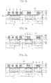
- FIGS. 1 a to 1 v A conventional method of fabricating a transistor of a DRAM (dynamic random access memory) semiconductor device will be described according to the prior art, referring to FIGS. 1 a to 1 v.
- DRAM dynamic random access memory
- a pad oxide layer 12 , a molding polysilicon layer 14 and a hard mask layer 16 are formed on a semiconductor substrate 10 that is doped with a P-type impurity.
- a photoresist is deposited on the hard mask layer 16 , and the photoresist is patterned through a photolithography process to expose a portion of the hard mask layer 16 .
- the hard mask layer 16 is selectively etched through the patterning of photoresist to expose the molding polysilicon layer 14 , thus defining an active region A.
- the molding polysilicon layer 14 , a pad oxide layer 12 and a semiconductor substrate 10 are partially removed to form a trench T.
- the surface of the exposed molding polysilicon layer 14 and semiconductor substrate 10 is selectively oxidized through a thermal oxide process by using the hard mask layer 16 as an oxide stop mask, and a device isolation film 18 is formed.
- the substrate is flattened so as to partially expose the semiconductor substrate.
- a photoresist 20 is deposited on the semiconductor substrate 10 , and the photoresist 20 is partially etched to expose a cell region X of the semiconductor substrate 10 .
- a P-type impurity of a low dose such as boron or BF 2 is selectively ion-implanted into the active region of the cell region X by using the photoresist 20 as an ion implantation mask, to form a channel impurity region 22 of low density, and then the photoresist 20 is removed.
- the photoresist 20 is deposited on the semiconductor substrate 10 , and the photoresist 20 is partially removed to expose an NMOS transistor region N of the circuit region Y of the semiconductor substrate 10 .
- a P-type impurity of a low dose such as boron or BF 2 is ion-implanted into the NMOS transistor region of the circuit region Y by using the photoresist 20 as an ion implantation mask to form the channel impurity region 22 of low density, and then the photoresist 20 is removed.
- the photoresist 20 is deposited on the semiconductor substrate 10 , and the photoresist 20 is partially removed to expose a PMOS transistor region P of the circuit region Y of the semiconductor substrate 10 .
- An N-type impurity of a low dose such as phosphorous or As is ion-implanted into the PMOS transistor region of the circuit region Y by using the photoresist 20 as an ion implantation mask to form the channel impurity region 22 of low density. Then the photoresist 20 is removed.
- a gate insulation layer 24 is formed with a predetermined thickness on the semiconductor substrate 10 through the use of a silicon oxide layer subject to a thermal oxide process, and a polysilicon gate electrode 26 is formed on the gate insulation layer 24 .
- the photoresist 20 is deposited on the substrate, and the photoresist 20 is partially removed to expose the gate electrode 26 of the NMOS transistor region N of the cell region Y and the circuit region X by using the photolithography process.
- An N-type impurity is implanted into the gate electrode 26 of the NMOS transistor region N of the cell region Y and the circuit region X, and then the photoresist 20 is removed.
- the photoresist 20 is deposited on the substrate, and the photoresist 20 is partially removed to expose the gate electrode 26 of the PMOS transistor region P of the circuit region Y by using the photolithography process.
- a P-type impurity is implanted into the gate electrode 26 of the PMOS transistor region P, and then the photoresist 20 is removed.
- a conductive metal layer 28 is formed on the gate electrode 26 , and a gate upper insulation layer 30 is formed on the conductive metal layer 28 by using a silicon nitride layer, etc.
- the photoresist (not shown) is deposited on the gate upper insulation layer 30 , and the photoresist is partially removed through a photolithography process.
- the gate upper insulation layer 30 , the conductive metal layer 28 and the gate electrode 26 are partially removed to expose a portion of the gate insulation layer 24 by using the photoresist as an etch mask, and then the photoresist is removed.
- the photoresist 20 is deposited on an entire face of the substrate, and the photoresist 20 is partially removed to expose the cell region X.
- a N-type impurity of a low dose such as phosphorous or As is ion-implanted into an exposed source/drain region (S/D) by using the photoresist 20 and the upper insulation layer 30 as an ion implantation mask to form a first impurity region 32 of low density, and then the photoresist 20 is removed.
- the photoresist 20 is deposited on an entire face of the substrate, and the photoresist 20 is partially removed to expose the NMOS transistor region N of the circuit region Y.
- An N-type impurity of a low dose such as phosphorous or As is ion-implanted into the S/D by using the photoresist 20 and the upper insulation layer 30 of the circuit region Y as an ion implantation mask to form the first impurity region 32 of low density, and then the photoresist 20 is removed.
- the photoresist 20 is deposited on an entire face of the substrate, and the photoresist 20 is partially removed to expose the PMOS transistor region P of the circuit region Y.
- a P-type impurity of a low dose such as boron or BF 2 is ion-implanted into the S/D by using the photoresist 20 and the upper insulation layer 30 as an ion implantation mask to form the first impurity region 32 of low density, and then the photoresist 20 is removed.
- an annealing process of high temperature e.g. about 800° C.
- a silicon nitride layer is formed on an entire face of the substrate, and a spacer 34 is formed on a sidewall of the gate electrode 26 .
- the photoresist 20 is deposited on an entire face of the substrate, and the photoresist 20 is partially removed to expose the NMOS transistor region N of the circuit region Y.
- An N-type impurity of a high dose is ion-implanted by using the photoresist 20 , upper insulating layer 30 , and the spacer 34 as an ion implantation mask to form a second impurity region 36 of high density, and then the photoresist 20 is removed.
- the photoresist 20 is deposited on an entire face of the substrate, and the photoresist 20 is partially removed to expose the PMOS transistor region P of the circuit region Y.
- a P-type impurity of a high dose is ion-implanted by using the photoresist 20 , the upper insulating layer 30 , and the spacer 34 as an ion implantation mask to form the second impurity region 36 of high density, and then the photoresist 20 is removed.
- an interlayer insulation layer 38 is formed with silicon oxide on the semiconductor substrate 10 and then the interlayer insulation layer 38 is flattened to expose the gate upper insulation layer 30 and the spacer 34 through a chemical mechanical polishing (CMP) or an etch-back.
- CMP chemical mechanical polishing
- the photoresist 20 is deposited on the substrate, and the photoresist 20 is partially removed to expose the interlayer insulation layer 38 provided over the S/D of the cell region X. Further, parts of the interlayer insulation layer 38 are removed to expose the gate insulation layer 24 above the S/D by using the photoresist 20 as an etch mask, and then the photoresist 20 is removed.
- an N-type impurity of a high dose is ion-implanted by using the interlayer insulation layer 38 , the upper insulation layer 30 and the spacer 34 as an ion implantation mask to form the second impurity region 36 of high density in the S/D of the cell region X, and then the photoresist 20 is removed.
- the annealing process of high temperature e.g. about 800° C. is performed.
- the gate insulation layer 24 is removed (not shown) from the S/D of the cell region X, and a pad polysilicon layer 40 is formed by using polysilicon containing a conductive impurity on the semiconductor substrate 10 .
- the pad polysilicon layer 40 is flattened through CMP or etch back so as to partially expose the spacer and the upper insulation layer 30 . Then, the annealing process of a high temperature is performed, thus reducing possible defects on the surface of the semiconductor substrate 10 comprising the S/D below the pad polysilicon layer 40 .
- an interlayer insulation layer is formed on the pad polysilicon layer 40 . Further, the interlayer insulation layer above the source region is removed to form a first contact hole, and a bit line contact is formed to be electrically connected to the pad polysilicon layer 40 through the first contact hole. Then, another interlayer insulation layer is formed on the substrate, and both interlayer insulation layers above the drain region are removed, thus forming a second contact hole. Thereon, a storage electrode electrically connected to the pad polysilicon layer 40 of a cell transistor through the second contact hole, a dielectric layer and a plate electrode are formed sequentially, thereby completing a capacitor of a memory cell.
- Embodiments of the invention address these and other limitations in the prior art.
- Example embodiments of the present invention provide a method of fabricating a transistor of a DRAM semiconductor device, to increase a performance of the device by preventing penetration of P-type impurity into a gate insulation layer, the P-type impurity being ion-implanted into polysilicon layer.
- Example embodiments of the present invention provide a method of fabricating a transistor of a DRAM semiconductor device, to increase productivity by reducing the number of convention processes needed to fabricate the DRAM semiconductor.
- only a single ion implantation process of P-type impurity into a polysilicon layer of a PMOS transistor region is needed to fabricate the DRAM semiconductor.
- the process of ion implantating an N-type impurity into a polysilicon layer of an NMOS transistor region can be omitted.
- a method of fabricating a transistor of a DRAM semiconductor device includes; forming a device isolation film in a semiconductor substrate, ion-implanting a channel adjusting impurity into an active region of a cell region and a circuit region defined by the device isolation film, forming respective channel impurity regions, and forming a gate insulation layer by forming a silicon oxide layer and a silicon oxide nitride layer on the semiconductor substrate.
- an embodiment of the present invention may be included in the method of fabricating a transistor of a DRAM semiconductor device.
- This aspect includes forming an N-type impurity-doped polysilicon layer on the gate insulation layer, and forming a gate electrode by selectively ion-implanting a P-type impurity into the polysilicon layer formed in a PMOS transistor region of the circuit region.
- This option process saves the process of separately ion-implanting an N-type impurity into the gate electrode.
- the method further includes forming a conductive metal layer and a gate upper insulation layer on the gate electrode, and removing the gate upper insulation layer, the conductive metal layer and the gate electrode from above a source/drain region, to form a gate stack in a gate region.
- the method also includes forming a second impurity region in the source/drain region by using the gate stack as an ion implantation mask, forming a spacer on a sidewall of the gate electrode, and forming a third impurity region within the second impurity region by using the spacer and the gate upper insulation layer as an ion implantation mask.
- a different process is used as a substitute for forming a silicon oxide layer and a silicon oxide nitride layer on the semiconductor substrate.
- the process includes forming a silicon oxide layer on the semiconductor substrate, and then and then implanting a nitrogen component into the silicon oxide layer to form a gate insulation layer.
- FIGS. 1 a to 1 v are cross-sectional views illustrating a method of fabricating a DRAM semiconductor device according to the prior art.
- FIGS. 2 a to 2 v are cross-sectional views illustrating a method of fabricating a DRAM semiconductor device according to an embodiment of the present invention.
- FIGS. 3 a to 3 b are cross-sectional views comparing a polysilicon layer having an inventive random structure and a polysilicon layer having a conventional column structure.
- FIG. 4 is a graph comparing C-V characteristics of the polysilicon layers referred to in FIGS. 3 a and 3 b.
- FIG. 5 a is a graph showing C-V characteristics of a gate insulation layer employing a DPN system according to an embodiment of the present invention.
- FIG. 5 b is a graph showing C-V characteristics of a gate insulation layer based on a rapid thermal annealing (RTA) process.
- RTA rapid thermal annealing
- FIG. 6 is a graph comparing threshold voltages in instances of boron penetration with threshold voltages in instances of no boron penetration.
- a pad oxide layer 102 is formed on a semiconductor substrate 100 that is doped with a P-type impurity, and then a molding polysilicon layer 104 and a hard mask layer 106 are formed on the pad oxide layer 102 .
- the molding polysilicon layer 104 is formed through chemical vapor deposition (CVD), and the hard mask layer 106 is formed in-situ in the same chamber by using a silicon nitride or a silicon oxide nitride.
- a photoresist (not shown) is deposited on the hard mask layer 106 and is then patterned, and the hard mask layer 106 is selectively etched by using the photoresist as an etch mask to define an active region A.
- Anisotropic etching may be employed, using the molding polysilicon layer 104 as an etch stop layer.
- the molding polysilicon layer 104 , the pad oxide layer 102 and the semiconductor substrate 100 are partially removed by using the hard mask layer 106 as an etch mask, to thus form a trench T.
- the trench T is formed with a predetermined depth, e.g. about 2000 to 5000 ⁇ .
- a device isolation film 108 is formed in the trench T. Then the exposed surface of the molding polysilicon layer 104 and the semiconductor substrate 100 is selectively oxidized through a thermal oxide process by using the hard mask layer 106 as an oxide stop mask.
- the molding polysilicon layer 104 serves as a buffer layer for mitigating stress from volume expansion generated in forming the device isolation film 108 . Further, the substrate is flattened through CMP or etch back. This flattening is performed to flatten the surface of the semiconductor substrate 100 by removing the hard mask layer 106 , the molding polysilicon layer 104 and the pad oxide layer 102 .
- a photoresist 110 is deposited on an entire face of the semiconductor substrate 100 , and the photoresist 110 is partially removed to expose a cell region X of the semiconductor substrate 100 through.
- a P-type impurity such as boron or BF 2 having a low dose, e.g. about 1.0 ⁇ 10 13 atoms/cm 3 , is selectively ion-implanted into the cell region X by using the photoresist 110 as an ion implantation mask to form a channel impurity region 112 of low density, e.g. about 1.0 ⁇ 10 17 atoms/cm 3 . Then the photoresist 110 is removed.
- a first channel stopper of high density may be formed with a predetermined depth, e.g. under about 2000 ⁇ , from the surface of the semiconductor substrate 100 by ion-implanting a P-type impurity of a high dose into the cell region X of the semiconductor substrate 100 before or after forming the channel impurity region 1112 .
- the photoresist 110 is deposited on an entire face of the semiconductor substrate 100 , and the photoresist 110 is partially removed to expose an NMOS transistor region N of the circuit region Y through a photolithography process.
- a P-type impurity such as boron or BF 2 having a low dose, e.g. about 1.0 ⁇ 10 13 atoms/cm 3 , is ion-implanted into the NMOS transistor region N of the circuit region Y by using the photoresist 110 as an ion implantation mask to form the channel impurity region 112 of low density, e.g. about 1.0 ⁇ 10 17 atoms/cm 3 . Then the photoresist 110 is removed.
- a first channel stopper of high density may be formed with a predetermined depth, e.g. under about 2000 ⁇ from the surface of the semiconductor substrate 100 , by ion-implanting a P-type impurity of a high dose into the NMOS transistor region N before or after forming the channel impurity region 112 .
- This solves the short-channel effect and prevents the bulk punch-through that is a main cause of the short-channel effect together with a shallow junction.
- the channel impurity region 112 and the first channel stopper may be formed individually or at the same time, in the cell region X and in the NMOS transistor region N of the circuit region Y. Further, the channel adjusting impurity region and the first channel stopper may have different densities to produce different threshold values in the respective transistors.
- the photoresist 110 is deposited on an entire face of the semiconductor substrate 100 , and the photoresist 110 is partially removed to expose a PMOS transistor region P of the circuit region Y of the semiconductor substrate 100 .
- An N-type impurity such as phosphorus or As having a low dose, e.g. about 1.0 ⁇ 10 13 atoms/cm 3 , is ion-implanted into the PMOS transistor region P of the circuit region Y by using the photoresist 110 as an ion implantation mask, to form the channel impurity region 112 of low density, e.g. about 1.0 ⁇ 10 17 atoms/cm 3 .
- the photoresist 110 is removed.
- the first channel stopper of high density may be formed with a predetermined depth, e.g. under about 2000 ⁇ from the surface of the semiconductor substrate 100 , by ion-implanting an N-type impurity of a high dose into the semiconductor substrate 100 before or after forming the channel impurity region 112 .
- a thermal oxide process is performed on the semiconductor substrate 100 to form a gate insulation layer 114 with a predetermined thickness, e.g. about 25 to 55 ⁇ .
- the gate insulation layer 114 may be formed by accumulating a silicon oxide layer and a silicon oxide nitride layer, or by implanting a nitrogen ion in a silicon oxide layer after forming a silicon oxide layer.
- a silicon oxide layer is formed on the semiconductor substrate 100 through a thermal oxide process within a sheet fed type process chamber such as a furnace through ISSG (in-situ steam generation) or RTO (rapid thermal oxidation). After the silicon oxide layer is formed over a predetermined thickness, e.g.
- ALD atomic-layer-deposited Si-nitride/SiO 2 stack gate dielectric system
- a decoupled plasma nitridation system (hereinafter, referred to as ‘DPN’) may be used, the DPN being used in a plasma apparatus that uses a reactive gas involving NO, NO 2 , or NH 3 gas, etc to form this silicon oxide and silicon nitride oxide structure.
- the silicon oxide layer is formed with about 30 ⁇ on the semiconductor substrate 100 , and the process chamber is at about 550 to 650° C. (preferably 595° C.), and DCS (SiH 2 Cl 2 ) and NH 3 gases are supplied individually and alternately into the process chamber for several seconds to several tens of seconds, e.g. 1 cycle thus forming a silicon oxide nitride layer of a thickness of about 1.0 to 1.4 ⁇ . If the DCS and NH 3 gases are individually supplied through 12 cycles, the silicon oxide nitride layer becomes about 12 ⁇ thick in the measured result using a transmission electron microscope (TEM).
- TEM transmission electron microscope
- the silicon oxide layer is formed with a thickness of about 45 ⁇ .
- the semiconductor substrate 100 on which the silicon oxide layer was formed is inserted into a plasma apparatus, where it is exposed below about 100° C. for about 50 to 100 seconds.
- the pressure within the plasma apparatus is maintained at about 7 to 15 mTorr, a power source of about 500 to 900 W is applied, and nitrogen and oxygen are implanted into the plasma apparatus for about 50 to 150 seconds.
- a post annealing process of about 850 to 950° C. is performed.
- the silicon oxide nitride layer on the silicon oxide layer will prevent penetration of an impurity such as boron or BF 2 into the channel when the impurity is being ion-implanted into a gate electrode.
- a gate electrode 116 is formed on the gate insulation layer 114 through CVD by using a polysilicon layer doped with an N-type impurity such as phosphorus or As of a high dose, e.g. 1.2 ⁇ 10 16 atoms/cm 3 .
- the N-type impurity of the doped polysilicon layer should be selected to avoid a depletion region being formed in the polysilicon layer having a predetermined density, e.g. about 2.0 ⁇ 10 20 atoms/cm 3 .
- the polysilicon layer is formed through CVD by using sheet fed type deposition equipment.
- a silicon layer of an amorphous state containing the N-type impurity is formed.
- the substrate is annealed at a predetermined temperature, e.g. about 520 to 550° C., for a predetermined time, e.g. about several tens of minutes, to form a disordered polysilicon layer.
- a photoresist 110 is deposited on an entire face of the substrate, and the photoresist is partially removed to expose the gate electrode 116 above the PMOS transistor region P of the circuit region Y.
- a P-type impurity such as boron or BF 2 of a high dose, e.g. about 1.2 ⁇ 10 16 atoms/cm 3 , is ion-implanted into the gate electrode 116 by using the photoresist as an ion implantation mask to form the gate electrode 116 of a high density, e.g. about 2.0 ⁇ 10 20 atoms/cm 3 .
- the P-type impurity should be selected to avoid depletion of the gate electrode 116 .
- the thickness of the polysilicon layer is about 300 to 1000 ⁇ (desirably, 800 ⁇ ).
- boron is used as the P-type impurity
- ion implantation is performed with about 10 KeV of energy, with a dose of about 1.2 ⁇ 10 16 atoms/cm 3 .
- boron is used, ion implantation is performed with about 2 to 5 KeV (desirably, 3 KeV) of energy with a dose of about 1.2 ⁇ 10 16 atoms/cm 3 .
- FIG. 3 a illustrates polysilicon having a grain boundary of a random structure
- FIG. 3 b illustrates poloysiclicon having a grain boundary of the conventional column structure
- the polysilicon having a grain boundary of a random structure based on the present invention acquires the random structure through annealing amorphous silicon to form polysilicon.
- the polysilicon of the conventional column structure acquires the column structure through low-pressure chemical vapor deposition
- the C-V characteristics of both structures were measured and plotted on a graph.
- the C-V was measured by applying a ground to the semiconductor substrate 100 doped with the N-type impurity and applying a bias voltage to the polysilicon layer and measuring the capacitance of the gate insulation layer 114 .
- the horizontal axis of FIG. 4 indicates the bias voltage (Vg) normalized for the measured capacitance.
- a C-V curved line (a) based on an N-type channel impurity region indicates a shift to a ‘ ⁇ ’ direction, and a flat band voltage indicates a shift to a ‘ ⁇ ’ direction, and a width of the C-V curved line is small to provide a stable electrical characteristic.
- a polysilicon referred to FIG. 3 a having a grain boundary of a random structure
- a C-V curved line (a) based on an N-type channel impurity region indicates a shift to a ‘ ⁇ ’ direction
- a flat band voltage indicates a shift to a ‘ ⁇ ’ direction
- a width of the C-V curved line is small to provide a stable electrical characteristic.
- a C-V curved line (b) indicates a shift to a ‘+’ direction
- a flat band voltage indicates a shift to a ‘+e’ direction
- a width of the C-V curved line is largely as compared with the C-V curved line of the invention.
- the polysilicon having the grain boundary of the random structure according to the present invention has a prominent C-V characteristic.
- the polysilicon of FIG. 3 a having the grain boundary of the random structure based on the present invention has a random structure by annealing amorphous silicon and forming polysilicon.
- a common electrode is contacted with the semiconductor substrate 100 doped with the N-type impurity, and an electrode having an applied bias voltage is contacted with the polysilicon layer, then a capacitance of the gate insulation layer 114 is measured by using a voltage difference between the common electrode and the bias voltage.
- a transverse axis of FIG. 4 indicates the bias voltage Vg and a longitudinal axis designates a value normalized for the capacitance value measured in the present invention.
- a shift of the capacitance value based on the bias voltage is represented as the C-V curved line according to an impurity density or a defect existing within the gate insulation layer 114 .
- the C-V curved lines are provided being almost overlapped, the C-V curved lines being for a case that the P-type impurity is not doped, namely, as an undoped poly, and being for a case that the P-type impurity such as boron or BF 2 is doped, namely, as a doped poly.
- a C-V curved line (DPN film) of the gate insulation 114 using the DPN system of the invention is shifted to a ‘ ⁇ ’ direction
- a C-V curved line (Conventional GNox) of the conventional gate insulation layer 114 is shifted to a ‘+’ direction.
- a width of the C-V curved line based on the invention is small as compared with the C-V curved line of the conventional gate insulation layer 114 , and the capacitance value based on the bias voltage is provided stably. That is, the gate insulation layer 114 employing the DPN system of the invention has a more prominent characteristic.
- the gate insulation layer 114 using the DPN system of the invention is obtained through the procedures that the silicon oxide layer is formed more thickly by considering the electrical characteristic and that the P-type impurity is ion implanted into the silicon oxide layer to form the silicon oxide nitride layer on the silicon oxide layer.
- the annealing process is performed with a rapid-thermal-annealing (RTA) process, as compared with such a case that the N-type and P-type impurities are ion implanted into the polysilicon layer formed on the gate insulation layer 114 , then the annealing process is not performed, namely, without the RTA.
- RTA rapid-thermal-annealing
- the transverse axis of FIG. 4 indicates the bias voltage Vg and the longitudinal axis designates the value normalized for the capacitance value measured in the present invention.
- a magnitude of a threshold voltage more increases if the gate region G increases.
- the magnitude of the threshold voltage is reduced according to the increase of the gate region G. That is, the gate insulation layer 114 of the present invention can control the boron penetration.
- a transverse axis of the FIG. 6 indicates a gate length and a longitudinal axis indicates a magnitude of threshold voltage.
- the gate region G of the invention has about 0.3 ⁇ m to 10 ⁇ m, and represents a shift of about several hundreds of mV regardless of a distance between the gate regions G.
- a diffusion constant of boron within a silicon compound layer of about 800° C. has about 1.0 ⁇ 10-8 cm 2 /s, more greatly by 10000 times than polysilicon, and an impurity absorption from the polysilicon to the silicon compound layer is caused on a high impurity diffusion within the polysilicon layer through a grain boundary diffusion.
- the P-type impurity is ion implanted into the polysilicon, then the rapid thermal annealing process is added at about 900° C. to 1000° C. for several seconds to several minutes for the sake of a dopant activation and a poly phase transition and so as to control the boron penetration, thereby enhancing a uniformity of threshold voltage Vth of a PMOS transistor.
- a metal layer 118 is formed with a predetermined thickness, e.g. about 1000 to 1200 ⁇ , on the gate electrode 116 , by using WSi x , TaSi 2 , or MoSi 2 , etc. and a gate upper insulation layer 120 is formed of silicon nitride on the metal layer 118 .
- a photoresist (not shown) is deposited on the gate upper insulation layer 120 . Then, the gate upper insulation layer 120 , the metal layer 118 and the gate electrode 116 are partially removed (as shown) to expose a portion of the gate insulation layer 114 by using the photoresist as an etch mask. Though not shown in the drawing, in forming an inverter (an AND gate and NOR gate circuit where the gate electrode 116 formed in the circuit region Y is grounded) the gate electrode 116 on the device isolation film 108 between the NMOS transistor region N and the PMOS transistor region P is removed to isolate the aforementioned electrodes.
- an inverter an AND gate and NOR gate circuit where the gate electrode 116 formed in the circuit region Y is grounded
- separating the gate electrode 116 of the NMOS transistor from the gate electrode 116 of the PMOS transistor at this time helps prevents an inter-diffusion between N-type and P-type impurities in the metal layer through a subsequent annealing process.
- the aforementioned inter-diffusion is undesirable because it will lower the performance of the device. After that, the photoresist is removed.
- a photoresist 110 is deposited on an entire face of the semiconductor substrate 100 , and the photoresist 110 is partially removed to expose the cell region X.
- An N-type impurity such as phosphorus or As of a low dose, e.g. 1.0 ⁇ 10 13 atoms/cm 3 , is ion-implanted into the S/D exposed by using the photoresist 110 and the gate upper insulation layer 120 as an ion implantation mask to form a first impurity region 122 of a low density, e.g. about 1.0 ⁇ 10 17 atoms/cm 3 .
- the photoresist 110 is removed.
- a second channel stopper may be formed with the P-type impurity before forming the first impurity region 122 to advantageously produce a tilt at a portion of the S/D and to invade a portion of the gate region G.
- This ion implantation process of the P-type impurity is performed at an energy of about 50 KeV so that the second channel stopper is formed at a depth of about 2000 ⁇ .
- the photoresist 110 is deposited on an entire face of the semiconductor substrate 100 , and the photoresist 110 is partially removed to expose the NMOS transistor region N of the circuit region Y.
- An N-type impurity such as phosphorus or As of a low dose, e.g. 1.0 ⁇ 10 13 atoms/cm 3 , is ion-implanted into the S/D by using the photoresist 110 and the gate upper insulation layer 120 as an ion implantation mask to form the first impurity region 122 of a low density, e.g. about 1.0 ⁇ 10 17 atoms/cm 3 . Then the photoresist 110 is removed.
- the second channel stopper may be formed with the P-type impurity before forming the first impurity region 122 , to advantageously produce a tilt at a portion of the S/D and to invade a portion of the gate region G.
- This ion implantation process of the P-type impurity is performed at an energy of about 50 KeV so that the second channel stopper is formed at a depth of about 2000 ⁇ .
- the photoresist 110 is deposited on an entire face of the semiconductor substrate 100 , and the photoresist 110 is partially removed to expose the PMOS transistor region P of the circuit region Y.
- a P-type impurity such as boron or BF 2 of a low dose, e.g. about 1.0 ⁇ 10 13 atoms/cm 3 , is ion-implanted into the S/D exposed by using the photoresist 110 and the gate upper insulation layer 120 as an ion implantation mask to form the first impurity region 122 of a low density, e.g. about 1.0 ⁇ 10 17 atoms/cm 3 .
- the photoresist 110 is removed.
- an annealing process at high temperature e.g. about 800° C.
- the second channel stopper may be formed with the N-type impurity before forming the first impurity region 122 to advantageously produce a tilt at a portion of the S/D and to invade a portion of the gate region G.
- This ion implantation process of the N-type impurity is performed at an energy of about 50 KeV so that the second channel stopper is formed at a depth of about 2000 ⁇ .
- a silicon nitride layer (not shown) is formed with a predetermined thickness on the substrate, and a photoresist (not shown) is deposited on the silicon nitride layer. The photoresist is partially removed to form a spacer 124 on a sidewall of the gate electrode 116 .
- the photoresist 110 is deposited on an entire face of the substrate, and the photoresist 110 is patterned to expose the NMOS transistor region N of the circuit region Y.
- An N-type impurity of a high dose e.g. about 1.2 ⁇ 10 16 atoms/cm 3
- the photoresist 110 is removed.
- This ion implantation process of the N-type impurity is performed at energy of about 50 KeV so that the second impurity region 126 is formed with a predetermined depth, e.g. about 1000 to 2000 ⁇ .
- the photoresist 110 is deposited on an entire face of the substrate, and the photoresist 110 is partially removed to expose the PMOS transistor region P of the circuit region Y.
- a P-type impurity of a high dose e.g. about 1.2 ⁇ 10 20 atoms/cm 3
- the photoresist 110 , the gate upper insulation layer 120 , and the spacer 124 as an ion implantation mask is ion-implanted by using the photoresist 110 , the gate upper insulation layer 120 , and the spacer 124 as an ion implantation mask to form the second impurity region 126 of a high density, e.g. about 2.0 ⁇ 10 20 atoms/cm 3 .
- This ion implantation process of the P-type impurity is performed at energy of about 50 KeV so that the second impurity region 126 is formed at a depth of about 2000 ⁇ .
- an interlayer insulation layer 128 is formed of silicon oxide on the substrate and is flattened through CMP or etch-back to expose the gate upper insulation layer 120 and a portion of the spacer 124 .
- the photoresist 110 is deposited on the interlayer insulation layer 128 , and the photoresist 110 and the interlayer insulation layer 128 are partially removed to expose the gate insulation layer 114 above the S/D of the cell region X. Next, the photoresist 110 is removed.
- an N-type impurity of a high dose e.g. about 1.2 ⁇ 10 20 atoms/cm 3
- the interlayer insulation layer 128 , the gate electrode 116 , and the spacer 124 as an ion implantation mask to form the second impurity region 126 of a high density, e.g. about 2.0 ⁇ 10 20 atoms/cm 3 .
- an annealing process of a high temperature e.g. about 800° C., is performed.
- a pad polysilicon layer 130 is formed of a polysilicon layer containing a conductive impurity on the semiconductor substrate 100 , and is flattened through CMP or etch-back to expose the gate upper insulation layer 120 and a portion of the spacer 124 . Then, an annealing process of a high temperature, e.g. about 830° C., is performed thus reducing possible defects on the surface of the semiconductor substrate 10 of the S/D below the pad polysilicon layer 130 .
- a high temperature e.g. about 830° C.
- an interlayer insulation layer is formed on the pad polysilicon layer 130 . Further, the interlayer insulation layer is removed above the source region S to form a first contact hole, and a bit line contact is formed to be electrically connected to the pad polysilicon layer 130 through the first contact hole. Then, another interlayer insulation layer is formed on the substrate, and both interlayer insulation layers are removed from above the drain region to form a second contact hole. Then a storage electrode electrically connected to the pad polysilicon layer 130 through the second contact hole, a dielectric layer, and a plate electrode are sequentially formed, thereby completing a capacitor of a memory cell.
- a gate insulation layer formed of a silicon oxide layer and a silicon oxide nitride layer is formed, and a P-type impurity is ion implanted into a polysilicon layer that is formed on the gate insulation layer.
- a polysilicon layer is formed through CVD using a reactive gas that contains an N-type impurity.
- a reactive gas that contains an N-type impurity can be avoided.
- a P-type impurity is then implanted into the polysilicon layer of a PMOS transistor region. Therefore, the number of the ion-implantation processes can be reduced, increasing productivity.
Abstract
Embodiments prevent or substantially reduce diffusion of a P-type impurity into a channel region in a PMOS transistor having a dual gate. Some embodiments include forming a device isolation film on a semiconductor substrate, forming a channel impurity region in an active region of the semiconductor substrate, and forming a gate insulation layer including a silicon oxide layer and a silicon oxide nitride layer on the semiconductor substrate. Also, the embodiments can include forming a polysilicon layer containing an N-type impurity on the gate insulation layer, and forming a gate electrode by selectively ion-implanting a P-type impurity into the polysilicon layer formed in a PMOS transistor region of the circuit region. The embodiments further include forming a conductive metal layer and a gate upper insulation layer on the gate electrode, and forming a gate stack in a gate region.
Description
This application is a divisional of U.S. patent application Ser. No. 10/922,055, filed Aug. 18, 2004, now pending, which is claims priority from Korean Patent Application No. 2003-0057836, filed on Aug. 21, 2003, the disclosure of which are incorporated herein in its entirety by reference.
The present invention relates to a manufacturing of a DRAM semiconductor device, and more particularly, to a transistor fabricating method capable of substantially reducing or controlling a penetration of impurity such as boron or BF2 in a PMOS transistor of a dual gate.
MOS (metal oxide silicon) devices are being made smaller and smaller according to a need for high-integration of semiconductor devices. For example, channel width is being reduced to sub-micron levels to increase the operating speed and current drive capability of semiconductor devices.
In a CMOS (complementary metal oxide silicon) semiconductor device a MOS device is generally used together with an NMOS transistor in which a P channel MOS transistor and an N-channel MOS transistor are formed in one semiconductor device so as to perform a complementary operation. Accordingly dual gates have been used. Dual gates generally reinforce the semiconductor function of a channel surface layer and therefore produce a desired symmetrical low-voltage operation. In fabricating a CMOS semiconductor device employing a dual gate, boron or BF2 is generally used to dope the polysilicon gate electrode of a PMOS transistor.
Unfortunately, when boron has been used as the impurity, it has been likely that the boron would penetrate a thin gate insulation layer and diffuse into the channel during a subsequent annealing process, etc. This diffusion of boron into the channel decreases the mobility of charges in the channel. Also, impurity depletion in the gate electrode may occur and may further form a P-type impurity layer near the channel connecting the source and drain. This results in increased an operating voltage, which of course hinders high integration. Furthermore, the operating voltage becomes unpredictable since boron does not always diffuse into the channel, making high integration even more difficult. This diffusion problem may become even more serious when BF2 is used as the impurity to make a shallower and narrower source/drain because boron is even more likely to diffuse when fluorine reactions are present.
Describing the aforementioned impurity depletion in the gate electrode in more detail, the solubility of solid boron in polysilicon is generally low. Therefore, even if the penetration of boron is high, the boron may not be distributed evenly within the polysilicon gate layer and a depleted region could form in the gate electrode adjacent to the gate insulation layer. If a depletion region forms adjacent to the gate insulation layer, a voltage applied to the gate electrode will not have a sufficient influence upon the channel. Therefore, the formation of a depletion region is another cause of an increase in the threshold voltage.
A conventional method of fabricating a transistor of a DRAM (dynamic random access memory) semiconductor device will be described according to the prior art, referring to FIGS. 1 a to 1 v.
Referring to FIG. 1 a, a pad oxide layer 12, a molding polysilicon layer 14 and a hard mask layer 16 are formed on a semiconductor substrate 10 that is doped with a P-type impurity.
Referring to FIG. 1 b, a photoresist is deposited on the hard mask layer 16, and the photoresist is patterned through a photolithography process to expose a portion of the hard mask layer 16. The hard mask layer 16 is selectively etched through the patterning of photoresist to expose the molding polysilicon layer 14, thus defining an active region A.
In FIG. 1 c, the molding polysilicon layer 14, a pad oxide layer 12 and a semiconductor substrate 10 are partially removed to form a trench T.
Referring to FIG. 1 d, the surface of the exposed molding polysilicon layer 14 and semiconductor substrate 10 is selectively oxidized through a thermal oxide process by using the hard mask layer 16 as an oxide stop mask, and a device isolation film 18 is formed. The substrate is flattened so as to partially expose the semiconductor substrate.
In FIG. 1 e, a photoresist 20 is deposited on the semiconductor substrate 10, and the photoresist 20 is partially etched to expose a cell region X of the semiconductor substrate 10. A P-type impurity of a low dose such as boron or BF2 is selectively ion-implanted into the active region of the cell region X by using the photoresist 20 as an ion implantation mask, to form a channel impurity region 22 of low density, and then the photoresist 20 is removed.
With reference to FIG. 1 f, the photoresist 20 is deposited on the semiconductor substrate 10, and the photoresist 20 is partially removed to expose an NMOS transistor region N of the circuit region Y of the semiconductor substrate 10. A P-type impurity of a low dose such as boron or BF2 is ion-implanted into the NMOS transistor region of the circuit region Y by using the photoresist 20 as an ion implantation mask to form the channel impurity region 22 of low density, and then the photoresist 20 is removed.
With reference to FIG. 1 g, the photoresist 20 is deposited on the semiconductor substrate 10, and the photoresist 20 is partially removed to expose a PMOS transistor region P of the circuit region Y of the semiconductor substrate 10. An N-type impurity of a low dose such as phosphorous or As is ion-implanted into the PMOS transistor region of the circuit region Y by using the photoresist 20 as an ion implantation mask to form the channel impurity region 22 of low density. Then the photoresist 20 is removed.
In FIG. 1 h, a gate insulation layer 24 is formed with a predetermined thickness on the semiconductor substrate 10 through the use of a silicon oxide layer subject to a thermal oxide process, and a polysilicon gate electrode 26 is formed on the gate insulation layer 24.
In FIG. 1 i, the photoresist 20 is deposited on the substrate, and the photoresist 20 is partially removed to expose the gate electrode 26 of the NMOS transistor region N of the cell region Y and the circuit region X by using the photolithography process. An N-type impurity is implanted into the gate electrode 26 of the NMOS transistor region N of the cell region Y and the circuit region X, and then the photoresist 20 is removed.
In FIG. 1 j, the photoresist 20 is deposited on the substrate, and the photoresist 20 is partially removed to expose the gate electrode 26 of the PMOS transistor region P of the circuit region Y by using the photolithography process. A P-type impurity is implanted into the gate electrode 26 of the PMOS transistor region P, and then the photoresist 20 is removed.
In FIG. 1 k, a conductive metal layer 28 is formed on the gate electrode 26, and a gate upper insulation layer 30 is formed on the conductive metal layer 28 by using a silicon nitride layer, etc.
Referring to FIG. 1 l, the photoresist (not shown) is deposited on the gate upper insulation layer 30, and the photoresist is partially removed through a photolithography process. Next, the gate upper insulation layer 30, the conductive metal layer 28 and the gate electrode 26 are partially removed to expose a portion of the gate insulation layer 24 by using the photoresist as an etch mask, and then the photoresist is removed.
In FIG. 1 m, the photoresist 20 is deposited on an entire face of the substrate, and the photoresist 20 is partially removed to expose the cell region X. A N-type impurity of a low dose such as phosphorous or As is ion-implanted into an exposed source/drain region (S/D) by using the photoresist 20 and the upper insulation layer 30 as an ion implantation mask to form a first impurity region 32 of low density, and then the photoresist 20 is removed.
In FIG. 1 n, the photoresist 20 is deposited on an entire face of the substrate, and the photoresist 20 is partially removed to expose the NMOS transistor region N of the circuit region Y. An N-type impurity of a low dose such as phosphorous or As is ion-implanted into the S/D by using the photoresist 20 and the upper insulation layer 30 of the circuit region Y as an ion implantation mask to form the first impurity region 32 of low density, and then the photoresist 20 is removed.
In FIG. 1 o, the photoresist 20 is deposited on an entire face of the substrate, and the photoresist 20 is partially removed to expose the PMOS transistor region P of the circuit region Y. A P-type impurity of a low dose such as boron or BF2 is ion-implanted into the S/D by using the photoresist 20 and the upper insulation layer 30 as an ion implantation mask to form the first impurity region 32 of low density, and then the photoresist 20 is removed. Subsequently, in order to reduce a lattice defect of the semiconductor substrate 10 generated by the ion implantation, an annealing process of high temperature, e.g. about 800° C., is performed.
With reference to FIG. 1 p, a silicon nitride layer is formed on an entire face of the substrate, and a spacer 34 is formed on a sidewall of the gate electrode 26.
In FIG. 1 q, the photoresist 20 is deposited on an entire face of the substrate, and the photoresist 20 is partially removed to expose the NMOS transistor region N of the circuit region Y. An N-type impurity of a high dose is ion-implanted by using the photoresist 20, upper insulating layer 30, and the spacer 34 as an ion implantation mask to form a second impurity region 36 of high density, and then the photoresist 20 is removed.
In FIG. 1 r, the photoresist 20 is deposited on an entire face of the substrate, and the photoresist 20 is partially removed to expose the PMOS transistor region P of the circuit region Y. A P-type impurity of a high dose is ion-implanted by using the photoresist 20, the upper insulating layer 30, and the spacer 34 as an ion implantation mask to form the second impurity region 36 of high density, and then the photoresist 20 is removed.
In FIG. 1 s, an interlayer insulation layer 38 is formed with silicon oxide on the semiconductor substrate 10 and then the interlayer insulation layer 38 is flattened to expose the gate upper insulation layer 30 and the spacer 34 through a chemical mechanical polishing (CMP) or an etch-back.
In FIG. 1 t, the photoresist 20 is deposited on the substrate, and the photoresist 20 is partially removed to expose the interlayer insulation layer 38 provided over the S/D of the cell region X. Further, parts of the interlayer insulation layer 38 are removed to expose the gate insulation layer 24 above the S/D by using the photoresist 20 as an etch mask, and then the photoresist 20 is removed.
With reference to FIG. 1 u, an N-type impurity of a high dose is ion-implanted by using the interlayer insulation layer 38, the upper insulation layer 30 and the spacer 34 as an ion implantation mask to form the second impurity region 36 of high density in the S/D of the cell region X, and then the photoresist 20 is removed. After the ion-implantation process, the annealing process of high temperature, e.g. about 800° C. is performed.
In FIG. 1 v, the gate insulation layer 24 is removed (not shown) from the S/D of the cell region X, and a pad polysilicon layer 40 is formed by using polysilicon containing a conductive impurity on the semiconductor substrate 10. The pad polysilicon layer 40 is flattened through CMP or etch back so as to partially expose the spacer and the upper insulation layer 30. Then, the annealing process of a high temperature is performed, thus reducing possible defects on the surface of the semiconductor substrate 10 comprising the S/D below the pad polysilicon layer 40.
Though not shown in the drawing, an interlayer insulation layer is formed on the pad polysilicon layer 40. Further, the interlayer insulation layer above the source region is removed to form a first contact hole, and a bit line contact is formed to be electrically connected to the pad polysilicon layer 40 through the first contact hole. Then, another interlayer insulation layer is formed on the substrate, and both interlayer insulation layers above the drain region are removed, thus forming a second contact hole. Thereon, a storage electrode electrically connected to the pad polysilicon layer 40 of a cell transistor through the second contact hole, a dielectric layer and a plate electrode are formed sequentially, thereby completing a capacitor of a memory cell.
However, there are problems in the method of fabricating the transistor of semiconductor device according to the prior art. When ion-implanting the P-type impurity into the gate electrode of the PMOS transistor region, the P-type impurity penetrates the gate insulation layer during a subsequent annealing process and diffuses into the channel. This results in a drop in device performance.
Furthermore, ion-implanting impurities into the gate electrode must be performed several times. Thus, the ion-implantation process is complicated, lowering productivity. Embodiments of the invention address these and other limitations in the prior art.
Example embodiments of the present invention provide a method of fabricating a transistor of a DRAM semiconductor device, to increase a performance of the device by preventing penetration of P-type impurity into a gate insulation layer, the P-type impurity being ion-implanted into polysilicon layer.
Example embodiments of the present invention provide a method of fabricating a transistor of a DRAM semiconductor device, to increase productivity by reducing the number of convention processes needed to fabricate the DRAM semiconductor. In one embodiment, only a single ion implantation process of P-type impurity into a polysilicon layer of a PMOS transistor region is needed to fabricate the DRAM semiconductor. The process of ion implantating an N-type impurity into a polysilicon layer of an NMOS transistor region can be omitted.
According to one feature of an embodiment of the present invention, a method of fabricating a transistor of a DRAM semiconductor device includes; forming a device isolation film in a semiconductor substrate, ion-implanting a channel adjusting impurity into an active region of a cell region and a circuit region defined by the device isolation film, forming respective channel impurity regions, and forming a gate insulation layer by forming a silicon oxide layer and a silicon oxide nitride layer on the semiconductor substrate.
Optionally another feature of an embodiment of the present invention may be included in the method of fabricating a transistor of a DRAM semiconductor device. This aspect includes forming an N-type impurity-doped polysilicon layer on the gate insulation layer, and forming a gate electrode by selectively ion-implanting a P-type impurity into the polysilicon layer formed in a PMOS transistor region of the circuit region. This option process saves the process of separately ion-implanting an N-type impurity into the gate electrode.
The method further includes forming a conductive metal layer and a gate upper insulation layer on the gate electrode, and removing the gate upper insulation layer, the conductive metal layer and the gate electrode from above a source/drain region, to form a gate stack in a gate region. The method also includes forming a second impurity region in the source/drain region by using the gate stack as an ion implantation mask, forming a spacer on a sidewall of the gate electrode, and forming a third impurity region within the second impurity region by using the spacer and the gate upper insulation layer as an ion implantation mask.
According to another feature of an embodiment of the present invention, a different process is used as a substitute for forming a silicon oxide layer and a silicon oxide nitride layer on the semiconductor substrate. The process includes forming a silicon oxide layer on the semiconductor substrate, and then and then implanting a nitrogen component into the silicon oxide layer to form a gate insulation layer.
The above and other features of exemplary embodiment of the present invention will become readily apparent from the description of the exemplary embodiments that follows, with reference to the attached drawing in which:
Hereinafter, example embodiments of the present invention will be described in detail with reference to FIGS. 2 to 6 . This invention may be embodied in many different forms and should not be construed as being limited to the example embodiments set forth herein; rather, these example embodiments are provided so that this disclosure is thorough and complete, and conveys the concept of the invention to those skilled in the art. It will be understood that when an element such as a layer, region or substrate is referred to as being “on” or “onto” another element, it can be directly on the other element or intervening elements may also be present. Additionally, the layer, region or substrate could be partially within or partially embedded in the another element. For example, a formation of layers on a semiconductor substrate or other layer in the accompanied drawings can be changed to a direct contacted formation or a formation of a third layer thereon.
Referring first to FIG. 2 a, a pad oxide layer 102 is formed on a semiconductor substrate 100 that is doped with a P-type impurity, and then a molding polysilicon layer 104 and a hard mask layer 106 are formed on the pad oxide layer 102. The molding polysilicon layer 104 is formed through chemical vapor deposition (CVD), and the hard mask layer 106 is formed in-situ in the same chamber by using a silicon nitride or a silicon oxide nitride.
Referring to FIG. 2 b, a photoresist (not shown) is deposited on the hard mask layer 106 and is then patterned, and the hard mask layer 106 is selectively etched by using the photoresist as an etch mask to define an active region A. Anisotropic etching may be employed, using the molding polysilicon layer 104 as an etch stop layer.
In FIG. 2 c, the molding polysilicon layer 104, the pad oxide layer 102 and the semiconductor substrate 100 are partially removed by using the hard mask layer 106 as an etch mask, to thus form a trench T. At this time, the trench T is formed with a predetermined depth, e.g. about 2000 to 5000 Å.
In FIG. 2 d, a device isolation film 108 is formed in the trench T. Then the exposed surface of the molding polysilicon layer 104 and the semiconductor substrate 100 is selectively oxidized through a thermal oxide process by using the hard mask layer 106 as an oxide stop mask. The molding polysilicon layer 104 serves as a buffer layer for mitigating stress from volume expansion generated in forming the device isolation film 108. Further, the substrate is flattened through CMP or etch back. This flattening is performed to flatten the surface of the semiconductor substrate 100 by removing the hard mask layer 106, the molding polysilicon layer 104 and the pad oxide layer 102.
With reference to FIG. 2 e, a photoresist 110 is deposited on an entire face of the semiconductor substrate 100, and the photoresist 110 is partially removed to expose a cell region X of the semiconductor substrate 100 through. A P-type impurity such as boron or BF2 having a low dose, e.g. about 1.0×10¹³ atoms/cm3, is selectively ion-implanted into the cell region X by using the photoresist 110 as an ion implantation mask to form a channel impurity region 112 of low density, e.g. about 1.0×10¹⁷ atoms/cm3. Then the photoresist 110 is removed. Though not shown in the drawing, a first channel stopper of high density may be formed with a predetermined depth, e.g. under about 2000 Å, from the surface of the semiconductor substrate 100 by ion-implanting a P-type impurity of a high dose into the cell region X of the semiconductor substrate 100 before or after forming the channel impurity region 1112. This solves a short-channel effect and prevents a bulk punch-through that is a main cause of the short-channel effect together with a shallow junction.
With reference to FIG. 2 f, the photoresist 110 is deposited on an entire face of the semiconductor substrate 100, and the photoresist 110 is partially removed to expose an NMOS transistor region N of the circuit region Y through a photolithography process. A P-type impurity such as boron or BF2 having a low dose, e.g. about 1.0×10¹³ atoms/cm3, is ion-implanted into the NMOS transistor region N of the circuit region Y by using the photoresist 110 as an ion implantation mask to form the channel impurity region 112 of low density, e.g. about 1.0×10¹⁷ atoms/cm3. Then the photoresist 110 is removed. Though not shown in the drawing, a first channel stopper of high density may be formed with a predetermined depth, e.g. under about 2000 Å from the surface of the semiconductor substrate 100, by ion-implanting a P-type impurity of a high dose into the NMOS transistor region N before or after forming the channel impurity region 112. This solves the short-channel effect and prevents the bulk punch-through that is a main cause of the short-channel effect together with a shallow junction. At this time, the channel impurity region 112 and the first channel stopper may be formed individually or at the same time, in the cell region X and in the NMOS transistor region N of the circuit region Y. Further, the channel adjusting impurity region and the first channel stopper may have different densities to produce different threshold values in the respective transistors.
In FIG. 2 g, the photoresist 110 is deposited on an entire face of the semiconductor substrate 100, and the photoresist 110 is partially removed to expose a PMOS transistor region P of the circuit region Y of the semiconductor substrate 100. An N-type impurity such as phosphorus or As having a low dose, e.g. about 1.0×10¹³ atoms/cm3, is ion-implanted into the PMOS transistor region P of the circuit region Y by using the photoresist 110 as an ion implantation mask, to form the channel impurity region 112 of low density, e.g. about 1.0×10¹⁷ atoms/cm3. Then the photoresist 110 is removed. Though not shown in the drawing, the first channel stopper of high density may be formed with a predetermined depth, e.g. under about 2000 Å from the surface of the semiconductor substrate 100, by ion-implanting an N-type impurity of a high dose into the semiconductor substrate 100 before or after forming the channel impurity region 112. This solves the short-channel effect and prevents a bulk punch-through that is a main cause of the short-channel effect together with the shallow junction.
In FIG. 2 h, a thermal oxide process is performed on the semiconductor substrate 100 to form a gate insulation layer 114 with a predetermined thickness, e.g. about 25 to 55 Å. The gate insulation layer 114 may be formed by accumulating a silicon oxide layer and a silicon oxide nitride layer, or by implanting a nitrogen ion in a silicon oxide layer after forming a silicon oxide layer. In the later method, a silicon oxide layer is formed on the semiconductor substrate 100 through a thermal oxide process within a sheet fed type process chamber such as a furnace through ISSG (in-situ steam generation) or RTO (rapid thermal oxidation). After the silicon oxide layer is formed over a predetermined thickness, e.g. about 30 to 40 Å, a reactive gas and NO, NO2, or NH3 gas, etc. are implanted into the process chamber. Thus, a thermally nitrided oxide or reoxidized nitrided oxide is formed on the substrate. In other words, a silicon oxide nitride layer is formed on the silicon oxide layer through an atomic-layer-deposited (ALD) Si-nitride/SiO2 stack gate dielectric system (hereinafter, referred to as ‘ALD’).
Alternatively a decoupled plasma nitridation system (hereinafter, referred to as ‘DPN’) may be used, the DPN being used in a plasma apparatus that uses a reactive gas involving NO, NO2, or NH3 gas, etc to form this silicon oxide and silicon nitride oxide structure.
Referring back to the ALD method, the silicon oxide layer is formed with about 30 Å on the semiconductor substrate 100, and the process chamber is at about 550 to 650° C. (preferably 595° C.), and DCS (SiH2Cl2) and NH3 gases are supplied individually and alternately into the process chamber for several seconds to several tens of seconds, e.g. 1 cycle thus forming a silicon oxide nitride layer of a thickness of about 1.0 to 1.4 Å. If the DCS and NH3 gases are individually supplied through 12 cycles, the silicon oxide nitride layer becomes about 12 Å thick in the measured result using a transmission electron microscope (TEM).
Referring now back to the process of forming the silicon oxide nitride layer through DPN, the silicon oxide layer is formed with a thickness of about 45 Å. Next, the semiconductor substrate 100 on which the silicon oxide layer was formed is inserted into a plasma apparatus, where it is exposed below about 100° C. for about 50 to 100 seconds. Next, the pressure within the plasma apparatus is maintained at about 7 to 15 mTorr, a power source of about 500 to 900 W is applied, and nitrogen and oxygen are implanted into the plasma apparatus for about 50 to 150 seconds. Finally to counteract any possible defects caused by a nitrogen component implanted into the silicon oxide layer, a post annealing process of about 850 to 950° C. is performed.
The silicon oxide nitride layer on the silicon oxide layer will prevent penetration of an impurity such as boron or BF2 into the channel when the impurity is being ion-implanted into a gate electrode.
Referring to FIG. 2 i, a gate electrode 116 is formed on the gate insulation layer 114 through CVD by using a polysilicon layer doped with an N-type impurity such as phosphorus or As of a high dose, e.g. 1.2×10¹⁶ atoms/cm3. The N-type impurity of the doped polysilicon layer should be selected to avoid a depletion region being formed in the polysilicon layer having a predetermined density, e.g. about 2.0×10²⁰ atoms/cm3. First, the polysilicon layer is formed through CVD by using sheet fed type deposition equipment. Next, a silicon layer of an amorphous state containing the N-type impurity is formed. Then the substrate is annealed at a predetermined temperature, e.g. about 520 to 550° C., for a predetermined time, e.g. about several tens of minutes, to form a disordered polysilicon layer.
In FIG. 2 j, a photoresist 110 is deposited on an entire face of the substrate, and the photoresist is partially removed to expose the gate electrode 116 above the PMOS transistor region P of the circuit region Y. A P-type impurity such as boron or BF2 of a high dose, e.g. about 1.2×10¹⁶ atoms/cm3, is ion-implanted into the gate electrode 116 by using the photoresist as an ion implantation mask to form the gate electrode 116 of a high density, e.g. about 2.0×10²⁰ atoms/cm3. At this time, the P-type impurity should be selected to avoid depletion of the gate electrode 116. Furthermore, the thickness of the polysilicon layer, the type and dose quantity of the P-type impurity (boron may be used), and the amount of ion implantation energy, etc should be considered. In one embodiment, the thickness of the polysilicon layer is about 300 to 1000 Å (desirably, 800 Å). Further, if BF2 is used as the P-type impurity, ion implantation is performed with about 10 KeV of energy, with a dose of about 1.2×10¹⁶ atoms/cm3. If boron is used, ion implantation is performed with about 2 to 5 KeV (desirably, 3 KeV) of energy with a dose of about 1.2×10¹⁶ atoms/cm3.
Referring now to FIG. 4 , the C-V characteristics of both structures were measured and plotted on a graph. The C-V was measured by applying a ground to the semiconductor substrate 100 doped with the N-type impurity and applying a bias voltage to the polysilicon layer and measuring the capacitance of the gate insulation layer 114. The horizontal axis of FIG. 4 indicates the bias voltage (Vg) normalized for the measured capacitance.
With reference to FIGS. 3 a to 4, in a polysilicon referred to FIG. 3 a having a grain boundary of a random structure, a C-V curved line (a) based on an N-type channel impurity region indicates a shift to a ‘−’ direction, and a flat band voltage indicates a shift to a ‘−’ direction, and a width of the C-V curved line is small to provide a stable electrical characteristic. However, in a polysilicon referred to FIG. 3 b having a grain boundary of a conventional column structure, a C-V curved line (b) indicates a shift to a ‘+’ direction, and a flat band voltage indicates a shift to a ‘+e’ direction, and a width of the C-V curved line is largely as compared with the C-V curved line of the invention. Thus, the polysilicon having the grain boundary of the random structure according to the present invention has a prominent C-V characteristic. The polysilicon of FIG. 3 a having the grain boundary of the random structure based on the present invention has a random structure by annealing amorphous silicon and forming polysilicon. The polysilicon of FIG. 3 b having the grain boundary of the conventional column structure has a column structure by forming polysilicon through a low-pressure chemical vapor deposition. In the measure of the C-V curved line, a common electrode is contacted with the semiconductor substrate 100 doped with the N-type impurity, and an electrode having an applied bias voltage is contacted with the polysilicon layer, then a capacitance of the gate insulation layer 114 is measured by using a voltage difference between the common electrode and the bias voltage. Herewith, a transverse axis of FIG. 4 indicates the bias voltage Vg and a longitudinal axis designates a value normalized for the capacitance value measured in the present invention. Thus, a shift of the capacitance value based on the bias voltage is represented as the C-V curved line according to an impurity density or a defect existing within the gate insulation layer 114. Further, in the polysilicon having the random structure of the invention, the C-V curved lines are provided being almost overlapped, the C-V curved lines being for a case that the P-type impurity is not doped, namely, as an undoped poly, and being for a case that the P-type impurity such as boron or BF2 is doped, namely, as a doped poly. This designates that the P-type impurity did not penetrate into the inside of the gate insulation layer 114. In the meantime, referring to FIG. 5 a, a C-V curved line (DPN film) of the gate insulation 114 using the DPN system of the invention is shifted to a ‘−’ direction, and a C-V curved line (Conventional GNox) of the conventional gate insulation layer 114 is shifted to a ‘+’ direction. A width of the C-V curved line based on the invention is small as compared with the C-V curved line of the conventional gate insulation layer 114, and the capacitance value based on the bias voltage is provided stably. That is, the gate insulation layer 114 employing the DPN system of the invention has a more prominent characteristic. Herewith, a transverse axis of FIG. 5 a indicates a bias voltage Vg and a longitudinal axis designates a value normalized for the capacitance value measured in the present invention. The gate insulation layer 114 using the DPN system of the invention is obtained through the procedures that the silicon oxide layer is formed more thickly by considering the electrical characteristic and that the P-type impurity is ion implanted into the silicon oxide layer to form the silicon oxide nitride layer on the silicon oxide layer.
Referring to FIG. 5 b, it indicates that there is a prominent C-V characteristic in such a case that the N-type and P-type impurities are ion implanted into the polysilicon layer formed on the gate insulation layer 114, then the annealing process is performed with a rapid-thermal-annealing (RTA) process, as compared with such a case that the N-type and P-type impurities are ion implanted into the polysilicon layer formed on the gate insulation layer 114, then the annealing process is not performed, namely, without the RTA. Herewith, the transverse axis of FIG. 4 indicates the bias voltage Vg and the longitudinal axis designates the value normalized for the capacitance value measured in the present invention.
With reference to FIG. 6 , in the gate insulation layer 114 of the invention without the boron penetration, a magnitude of a threshold voltage more increases if the gate region G increases. However, in the conventional gate insulation layer 114 with the boron penetration, the magnitude of the threshold voltage is reduced according to the increase of the gate region G. That is, the gate insulation layer 114 of the present invention can control the boron penetration. Herewith, a transverse axis of the FIG. 6 indicates a gate length and a longitudinal axis indicates a magnitude of threshold voltage. At this time, the gate region G of the invention has about 0.3 μm to 10 μm, and represents a shift of about several hundreds of mV regardless of a distance between the gate regions G. If a real space is about 200 nm in a case of separating the gate region G from an edge of the respective gate regions G formed on the NMOS transistor region N and the PMOS transistor region P, it is clarified that there is no a characteristic shift. For reference, according to the cited references, a diffusion constant of boron within a silicon compound layer of about 800° C. has about 1.0×10⁻⁸ cm2/s, more greatly by 10000 times than polysilicon, and an impurity absorption from the polysilicon to the silicon compound layer is caused on a high impurity diffusion within the polysilicon layer through a grain boundary diffusion.
Therefore, in the fabricating method of the DRAM semiconductor transistor according to the present invention, the P-type impurity is ion implanted into the polysilicon, then the rapid thermal annealing process is added at about 900° C. to 1000° C. for several seconds to several minutes for the sake of a dopant activation and a poly phase transition and so as to control the boron penetration, thereby enhancing a uniformity of threshold voltage Vth of a PMOS transistor.
Referring to FIG. 2 k, a metal layer 118 is formed with a predetermined thickness, e.g. about 1000 to 1200 Å, on the gate electrode 116, by using WSix, TaSi2, or MoSi2, etc. and a gate upper insulation layer 120 is formed of silicon nitride on the metal layer 118.
In FIG. 21 , a photoresist (not shown) is deposited on the gate upper insulation layer 120. Then, the gate upper insulation layer 120, the metal layer 118 and the gate electrode 116 are partially removed (as shown) to expose a portion of the gate insulation layer 114 by using the photoresist as an etch mask. Though not shown in the drawing, in forming an inverter (an AND gate and NOR gate circuit where the gate electrode 116 formed in the circuit region Y is grounded) the gate electrode 116 on the device isolation film 108 between the NMOS transistor region N and the PMOS transistor region P is removed to isolate the aforementioned electrodes. Further, separating the gate electrode 116 of the NMOS transistor from the gate electrode 116 of the PMOS transistor at this time helps prevents an inter-diffusion between N-type and P-type impurities in the metal layer through a subsequent annealing process. The aforementioned inter-diffusion is undesirable because it will lower the performance of the device. After that, the photoresist is removed.
In FIG. 2 m, a photoresist 110 is deposited on an entire face of the semiconductor substrate 100, and the photoresist 110 is partially removed to expose the cell region X. An N-type impurity such as phosphorus or As of a low dose, e.g. 1.0×10¹³ atoms/cm3, is ion-implanted into the S/D exposed by using the photoresist 110 and the gate upper insulation layer 120 as an ion implantation mask to form a first impurity region 122 of a low density, e.g. about 1.0×10¹⁷ atoms/cm3. Then the photoresist 110 is removed. Though not shown in the drawing, a second channel stopper may be formed with the P-type impurity before forming the first impurity region 122 to advantageously produce a tilt at a portion of the S/D and to invade a portion of the gate region G. This ion implantation process of the P-type impurity is performed at an energy of about 50 KeV so that the second channel stopper is formed at a depth of about 2000 Å.
With reference to FIG. 2 n, the photoresist 110 is deposited on an entire face of the semiconductor substrate 100, and the photoresist 110 is partially removed to expose the NMOS transistor region N of the circuit region Y. An N-type impurity such as phosphorus or As of a low dose, e.g. 1.0×10¹³ atoms/cm3, is ion-implanted into the S/D by using the photoresist 110 and the gate upper insulation layer 120 as an ion implantation mask to form the first impurity region 122 of a low density, e.g. about 1.0×10¹⁷ atoms/cm3. Then the photoresist 110 is removed. Though not shown in the drawing, the second channel stopper may be formed with the P-type impurity before forming the first impurity region 122, to advantageously produce a tilt at a portion of the S/D and to invade a portion of the gate region G. This ion implantation process of the P-type impurity is performed at an energy of about 50 KeV so that the second channel stopper is formed at a depth of about 2000 Å.
Referring to FIG. 2 o, the photoresist 110 is deposited on an entire face of the semiconductor substrate 100, and the photoresist 110 is partially removed to expose the PMOS transistor region P of the circuit region Y. A P-type impurity such as boron or BF2 of a low dose, e.g. about 1.0×10¹³ atoms/cm3, is ion-implanted into the S/D exposed by using the photoresist 110 and the gate upper insulation layer 120 as an ion implantation mask to form the first impurity region 122 of a low density, e.g. about 1.0×10¹⁷ atoms/cm3. Then the photoresist 110 is removed. Subsequently, an annealing process at high temperature, e.g. about 800° C., is performed to reduce lattice defects of the silicon semiconductor substrate 100 that may be generated by the ion implantation. Though not shown in the drawing, the second channel stopper may be formed with the N-type impurity before forming the first impurity region 122 to advantageously produce a tilt at a portion of the S/D and to invade a portion of the gate region G. This ion implantation process of the N-type impurity is performed at an energy of about 50 KeV so that the second channel stopper is formed at a depth of about 2000 Å.
With reference to FIG. 2 p, a silicon nitride layer (not shown) is formed with a predetermined thickness on the substrate, and a photoresist (not shown) is deposited on the silicon nitride layer. The photoresist is partially removed to form a spacer 124 on a sidewall of the gate electrode 116.
In FIG. 2 q, the photoresist 110 is deposited on an entire face of the substrate, and the photoresist 110 is patterned to expose the NMOS transistor region N of the circuit region Y. An N-type impurity of a high dose, e.g. about 1.2×10¹⁶ atoms/cm3, is ion-implanted by using the photoresist 110, the gate upper insulation layer 120, and the spacer 124 as an ion implantation mask to form a second impurity region 126 of a high density, e.g. about 2.0×10²⁰ atoms/cm3. Then the photoresist 110 is removed. This ion implantation process of the N-type impurity is performed at energy of about 50 KeV so that the second impurity region 126 is formed with a predetermined depth, e.g. about 1000 to 2000 Å.
Referring to FIG. 2 r, the photoresist 110 is deposited on an entire face of the substrate, and the photoresist 110 is partially removed to expose the PMOS transistor region P of the circuit region Y. A P-type impurity of a high dose, e.g. about 1.2×10²⁰ atoms/cm3, is ion-implanted by using the photoresist 110, the gate upper insulation layer 120, and the spacer 124 as an ion implantation mask to form the second impurity region 126 of a high density, e.g. about 2.0×10²⁰ atoms/cm3. Then the photoresist 110 is removed. This ion implantation process of the P-type impurity is performed at energy of about 50 KeV so that the second impurity region 126 is formed at a depth of about 2000 Å.
With reference to FIG. 2 s, an interlayer insulation layer 128 is formed of silicon oxide on the substrate and is flattened through CMP or etch-back to expose the gate upper insulation layer 120 and a portion of the spacer 124.
In FIG. 2 t, the photoresist 110 is deposited on the interlayer insulation layer 128, and the photoresist 110 and the interlayer insulation layer 128 are partially removed to expose the gate insulation layer 114 above the S/D of the cell region X. Next, the photoresist 110 is removed.
In FIG. 2 u, an N-type impurity of a high dose, e.g. about 1.2×10²⁰ atoms/cm3, is ion-implanted by using the interlayer insulation layer 128, the gate electrode 116, and the spacer 124 as an ion implantation mask to form the second impurity region 126 of a high density, e.g. about 2.0×10²⁰ atoms/cm3. Then, an annealing process of a high temperature, e.g. about 800° C., is performed.
Referring to FIG. 2 v, the gate insulation layer 114 is removed (not shown) from the S/D of the cell region X. A pad polysilicon layer 130 is formed of a polysilicon layer containing a conductive impurity on the semiconductor substrate 100, and is flattened through CMP or etch-back to expose the gate upper insulation layer 120 and a portion of the spacer 124. Then, an annealing process of a high temperature, e.g. about 830° C., is performed thus reducing possible defects on the surface of the semiconductor substrate 10 of the S/D below the pad polysilicon layer 130.
Though not shown in the drawing, an interlayer insulation layer is formed on the pad polysilicon layer 130. Further, the interlayer insulation layer is removed above the source region S to form a first contact hole, and a bit line contact is formed to be electrically connected to the pad polysilicon layer 130 through the first contact hole. Then, another interlayer insulation layer is formed on the substrate, and both interlayer insulation layers are removed from above the drain region to form a second contact hole. Then a storage electrode electrically connected to the pad polysilicon layer 130 through the second contact hole, a dielectric layer, and a plate electrode are sequentially formed, thereby completing a capacitor of a memory cell.
As was described above, in the method of fabricating a transistor according to the present invention, a gate insulation layer formed of a silicon oxide layer and a silicon oxide nitride layer is formed, and a P-type impurity is ion implanted into a polysilicon layer that is formed on the gate insulation layer. By doing so, a penetration of the P-type impurity into the gate insulation layer is prevented, thus increasing the performance of the device.
In addition, in forming a gate electrode a polysilicon layer is formed through CVD using a reactive gas that contains an N-type impurity. Thus, the process of separately implanting an N-type impurity into parts of the polysilicon layer can be avoided. A P-type impurity is then implanted into the polysilicon layer of a PMOS transistor region. Therefore, the number of the ion-implantation processes can be reduced, increasing productivity.
It will be apparent to those skilled in the art that modifications and variations can be made in the present invention without deviating from the spirit or scope of the invention. Thus, it is intended that the present invention cover any such modifications and variations of this invention provided they come within the scope of the appended claims and their equivalents. Accordingly, these and other changes and modifications are seen to be within the true spirit and scope of the invention as defined by the appended claims.
Claims (23)
1. A method of doping a polysilicon layer, comprising:
forming a gate insulation layer on a semiconductor substrate by using a silicon oxide layer and a silicon oxide nitride layer;
forming a polysilicon layer on the gate insulation layer;
annealing the polysilicon layer so that grain boundaries of the polysilicon layer have a substantially random structure;
before performing any other ion implantation and before removing material from the polysilicon layer, ion-implanting a P-type impurity into the polysilicon layer to form a gate electrode;
wherein the gate insulation layer substantially prevents the P-type impurity from diffusing into the semiconductor substrate, and
the polysilicon layer is annealed before ion-implanting the polysilicon layer with the P-type impurity.
2. The method as claimed in 1, wherein the gate insulation layer is formed with a thickness of 25 to 55 A.
3. The method as claimed in 1, wherein the silicon oxide layer in the gate insulation layer is formed by using a thermal oxide process.
4. The method as claimed in 1, wherein the gate insulation layer is formed in a furnace, an ISSG (in-situ steam generation) process chamber, or an RTO (rapid thermal oxidation) process chamber.
5. The method as claimed in 1, wherein the silicon oxide nitride layer in the gate insulation layer is formed under an atmosphere of NO, NO2 or NH3.
6. The method as claimed in 1, wherein the silicon oxide nitride layer is formed through an atomic-layer-deposition (ALD) system or a decoupled plasma nitridation (DPN) system.
7. The method as claimed in 6, wherein the ALD system includes forming the silicon oxide nitride layer at temperature of 550 to 650° C.
8. The method as claimed in 6, wherein the ALD system is performed by forming the silicon oxide nitride layer on the silicon oxide layer.
9. The method as claimed in 8, wherein the silicon oxide layer is formed with a thickness of about 30 to 40 A, and the silicon oxide nitride layer is formed with a thickness of about 10 to 25 A.
10. The method as claimed in 8, wherein the silicon oxide nitride layer is formed by using thermally nitrided oxide or reoxidized nitrided oxide.
11. The method as claimed in 6, wherein the ALD system is performed by alternately supplying DCS (SiH2Cl) and NH3 gas into a process chamber.
12. The method as claimed in 11, wherein the DCS (SiH2Cl) and NH3 gases are alternatively supplied into the process chamber at a supply cycle of about every several seconds to about every several tens of seconds.
13. The method as claimed in 11, wherein a thickness of the silicon oxide nitride layer is about 1.0 to 1.4 A depending on the length of the supply cycle.
14. The method as claimed in 6, wherein the DPN system comprises implanting a nitrogen ion into the silicon oxide layer.
15. The method as claimed in 6, wherein the DPN system further comprises forming the silicon oxide nitride layer below 100° C.
16. The method as claimed in 6, wherein the DPN system is performed for about 50 to 150 seconds.
17. The method as claimed in 6, wherein the DPN system is performed under a pressure of about 7 to 11 mTorr in a plasma apparatus.
18. The method as claimed in 6, wherein the DPN system is performed with a power source of about 500 or 900 W.
19. The method as claimed in 6, wherein the DPN system is performed by supplying NO, NO2, or NH3 gas into a plasma apparatus for about 50 to 110 seconds to form the silicon oxide nitride layer.
20. The method as claimed in 6, wherein the silicon oxide nitride layer formed through the use of the DPN system is post annealed.
21. The method as claimed in 20, wherein the post annealing process is performed at about 850 to 950° C.
22. The method as claimed in 20, wherein the post annealing process is performed for about 30 seconds.
23. A method of forming a CMOS semiconductor device, comprising:
forming a semiconductor substrate having an NMOS cell region and a circuit region having an NMOS region and a PMOS region;
forming a gate insulation layer including a silicon oxide layer and a silicon oxide nitride layer on the semiconductor substrate;
forming a polysilicon layer on the gate insulation layer;
annealing the polysilicon layer so that grain boundaries of the polysilicon layer have a substantially random structure;
before performing any other ion implantation, ion-implanting a P-type impurity into a portion of the polysilicon layer corresponding to the PMOS transistor; and
etching the polysilicon layer to form gate electrodes of at least the NMOS transistor of the cell region, the NMOS transistor of the circuit region, and the PMOS transistor of the circuit region,
wherein the polysilicon layer is annealed before ion-implanting the polysilicon layer with the P-type impurity.
Priority Applications (1)
| Application Number | Priority Date | Filing Date | Title |
|---|---|---|---|
| US11/738,620 US7833864B2 (en) | 2003-08-21 | 2007-04-23 | Method of doping polysilicon layer that utilizes gate insulation layer to prevent diffusion of ion implanted impurities into underlying semiconductor substrate |
Applications Claiming Priority (4)
| Application Number | Priority Date | Filing Date | Title |
|---|---|---|---|
| KR2003-0057836 | 2003-08-21 | ||
| KR1020030057836A KR100568859B1 (en) | 2003-08-21 | 2003-08-21 | Method for manufacturing transistor of dynamic random access memory semiconductor |
| US10/922,055 US7223649B2 (en) | 2003-08-21 | 2004-08-18 | Method of fabricating transistor of DRAM semiconductor device |
| US11/738,620 US7833864B2 (en) | 2003-08-21 | 2007-04-23 | Method of doping polysilicon layer that utilizes gate insulation layer to prevent diffusion of ion implanted impurities into underlying semiconductor substrate |
Related Parent Applications (1)
| Application Number | Title | Priority Date | Filing Date |
|---|---|---|---|
| US10/922,055 Division US7223649B2 (en) | 2003-08-21 | 2004-08-18 | Method of fabricating transistor of DRAM semiconductor device |
Publications (2)
| Publication Number | Publication Date |
|---|---|
| US20070190723A1 US20070190723A1 (en) | 2007-08-16 |
| US7833864B2 true US7833864B2 (en) | 2010-11-16 |
Family
ID=34192170
Family Applications (2)
| Application Number | Title | Priority Date | Filing Date |
|---|---|---|---|
| US10/922,055 Active 2025-03-16 US7223649B2 (en) | 2003-08-21 | 2004-08-18 | Method of fabricating transistor of DRAM semiconductor device |
| US11/738,620 Active 2026-02-14 US7833864B2 (en) | 2003-08-21 | 2007-04-23 | Method of doping polysilicon layer that utilizes gate insulation layer to prevent diffusion of ion implanted impurities into underlying semiconductor substrate |
Family Applications Before (1)
| Application Number | Title | Priority Date | Filing Date |
|---|---|---|---|
| US10/922,055 Active 2025-03-16 US7223649B2 (en) | 2003-08-21 | 2004-08-18 | Method of fabricating transistor of DRAM semiconductor device |
Country Status (2)
| Country | Link |
|---|---|
| US (2) | US7223649B2 (en) |
| KR (1) | KR100568859B1 (en) |
Families Citing this family (34)
| Publication number | Priority date | Publication date | Assignee | Title |
|---|---|---|---|---|
| KR101054320B1 (en) * | 2006-01-25 | 2011-08-05 | 후지쯔 세미컨덕터 가부시키가이샤 | Method for manufacturing semiconductor device |
| US20090117701A1 (en) * | 2007-11-01 | 2009-05-07 | Meng-Yi Wu | Method for manufacturing a mos transistor |
| KR101057188B1 (en) * | 2008-11-11 | 2011-08-16 | 주식회사 하이닉스반도체 | Method for manufacturing PMOS transistor and method for forming dual gate of semiconductor device using same |
| US9611544B2 (en) | 2010-04-15 | 2017-04-04 | Novellus Systems, Inc. | Plasma activated conformal dielectric film deposition |
| US9892917B2 (en) | 2010-04-15 | 2018-02-13 | Lam Research Corporation | Plasma assisted atomic layer deposition of multi-layer films for patterning applications |
| US8728956B2 (en) | 2010-04-15 | 2014-05-20 | Novellus Systems, Inc. | Plasma activated conformal film deposition |
| US8637411B2 (en) | 2010-04-15 | 2014-01-28 | Novellus Systems, Inc. | Plasma activated conformal dielectric film deposition |
| US9373500B2 (en) | 2014-02-21 | 2016-06-21 | Lam Research Corporation | Plasma assisted atomic layer deposition titanium oxide for conformal encapsulation and gapfill applications |
| US9390909B2 (en) | 2013-11-07 | 2016-07-12 | Novellus Systems, Inc. | Soft landing nanolaminates for advanced patterning |
| US9076646B2 (en) | 2010-04-15 | 2015-07-07 | Lam Research Corporation | Plasma enhanced atomic layer deposition with pulsed plasma exposure |
| US8956983B2 (en) | 2010-04-15 | 2015-02-17 | Novellus Systems, Inc. | Conformal doping via plasma activated atomic layer deposition and conformal film deposition |
| US9997357B2 (en) | 2010-04-15 | 2018-06-12 | Lam Research Corporation | Capped ALD films for doping fin-shaped channel regions of 3-D IC transistors |
| US9257274B2 (en) | 2010-04-15 | 2016-02-09 | Lam Research Corporation | Gapfill of variable aspect ratio features with a composite PEALD and PECVD method |
| US9685320B2 (en) | 2010-09-23 | 2017-06-20 | Lam Research Corporation | Methods for depositing silicon oxide |
| US8524612B2 (en) | 2010-09-23 | 2013-09-03 | Novellus Systems, Inc. | Plasma-activated deposition of conformal films |
| EP2472573A1 (en) * | 2011-01-04 | 2012-07-04 | Nxp B.V. | Vertical transistor manufacturing method and vertical transistor |
| US8647993B2 (en) | 2011-04-11 | 2014-02-11 | Novellus Systems, Inc. | Methods for UV-assisted conformal film deposition |
| US8592328B2 (en) | 2012-01-20 | 2013-11-26 | Novellus Systems, Inc. | Method for depositing a chlorine-free conformal sin film |
| US8728955B2 (en) | 2012-02-14 | 2014-05-20 | Novellus Systems, Inc. | Method of plasma activated deposition of a conformal film on a substrate surface |
| US9355839B2 (en) | 2012-10-23 | 2016-05-31 | Lam Research Corporation | Sub-saturated atomic layer deposition and conformal film deposition |
| JP6538300B2 (en) | 2012-11-08 | 2019-07-03 | ノベラス・システムズ・インコーポレーテッドNovellus Systems Incorporated | Method for depositing a film on a sensitive substrate |
| SG2013083241A (en) | 2012-11-08 | 2014-06-27 | Novellus Systems Inc | Conformal film deposition for gapfill |
| US9214334B2 (en) | 2014-02-18 | 2015-12-15 | Lam Research Corporation | High growth rate process for conformal aluminum nitride |
| US9478438B2 (en) | 2014-08-20 | 2016-10-25 | Lam Research Corporation | Method and apparatus to deposit pure titanium thin film at low temperature using titanium tetraiodide precursor |
| US9478411B2 (en) | 2014-08-20 | 2016-10-25 | Lam Research Corporation | Method to tune TiOx stoichiometry using atomic layer deposited Ti film to minimize contact resistance for TiOx/Ti based MIS contact scheme for CMOS |
| US9564312B2 (en) | 2014-11-24 | 2017-02-07 | Lam Research Corporation | Selective inhibition in atomic layer deposition of silicon-containing films |
| US10566187B2 (en) | 2015-03-20 | 2020-02-18 | Lam Research Corporation | Ultrathin atomic layer deposition film accuracy thickness control |
| US9502238B2 (en) | 2015-04-03 | 2016-11-22 | Lam Research Corporation | Deposition of conformal films by atomic layer deposition and atomic layer etch |
| US10526701B2 (en) | 2015-07-09 | 2020-01-07 | Lam Research Corporation | Multi-cycle ALD process for film uniformity and thickness profile modulation |
| US9773643B1 (en) | 2016-06-30 | 2017-09-26 | Lam Research Corporation | Apparatus and method for deposition and etch in gap fill |
| US10062563B2 (en) | 2016-07-01 | 2018-08-28 | Lam Research Corporation | Selective atomic layer deposition with post-dose treatment |
| US10037884B2 (en) | 2016-08-31 | 2018-07-31 | Lam Research Corporation | Selective atomic layer deposition for gapfill using sacrificial underlayer |
| US10269559B2 (en) | 2017-09-13 | 2019-04-23 | Lam Research Corporation | Dielectric gapfill of high aspect ratio features utilizing a sacrificial etch cap layer |
| CN110854075B (en) * | 2019-11-13 | 2022-10-18 | 上海华力集成电路制造有限公司 | CMOS device manufacturing method |
Citations (18)
| Publication number | Priority date | Publication date | Assignee | Title |
|---|---|---|---|---|
| US6001677A (en) | 1997-04-25 | 1999-12-14 | Ricoh Company, Ltd. | Method for fabricating CMOS transistors by implanting into polysilicon |
| US6030874A (en) | 1997-01-21 | 2000-02-29 | Texas Instruments Incorporated | Doped polysilicon to retard boron diffusion into and through thin gate dielectrics |
| KR100266690B1 (en) | 1998-05-21 | 2000-09-15 | 김영환 | Method for fabricating dual gate of semiconductor device |
| US6184110B1 (en) | 1998-04-30 | 2001-02-06 | Sharp Laboratories Of America, Inc. | Method of forming nitrogen implanted ultrathin gate oxide for dual gate CMOS devices |
| US6198121B1 (en) | 1997-05-15 | 2001-03-06 | Vanguard International Semiconductor Corporation | Method fabricating a DRAM cell with an area equal to four times the used minimum feature |
| US20020001899A1 (en) | 2000-06-15 | 2002-01-03 | Fumitoshi Ito | Semiconductor integrated circuit device and a method of manufacturing the same |
| KR20020002155A (en) | 2000-06-29 | 2002-01-09 | 박종섭 | Method for forming dual gate electrode of semiconductor device |
| US6387784B1 (en) | 2001-03-19 | 2002-05-14 | Chartered Semiconductor Manufacturing Ltd. | Method to reduce polysilicon depletion in MOS transistors |
| US20020068405A1 (en) * | 2000-11-30 | 2002-06-06 | Atsuki Ono | Fabrication method for a semiconductor integrated circuit device |
| US6413881B1 (en) * | 2000-03-09 | 2002-07-02 | Lsi Logic Corporation | Process for forming thin gate oxide with enhanced reliability by nitridation of upper surface of gate of oxide to form barrier of nitrogen atoms in upper surface region of gate oxide, and resulting product |
| US6432780B2 (en) | 2000-01-30 | 2002-08-13 | Wei-Wen Chen | Method for suppressing boron penetrating gate dielectric layer by pulsed nitrogen plasma doping |
| US6489210B1 (en) | 1999-01-12 | 2002-12-03 | Hyundai Electronics Co., Ltd. | Method for forming dual gate in DRAM embedded with a logic circuit |
| US20030057499A1 (en) | 2000-01-24 | 2003-03-27 | Naoki Yamamoto | Method of manufacturing a dual gate semiconductor device with a poly-metal electrode |
| US20030092249A1 (en) | 2001-11-09 | 2003-05-15 | Chia-Fu Hsu | Lightly-insitu-doped amorphous silicon applied in DRAM gates |
| US6566281B1 (en) | 1997-10-15 | 2003-05-20 | International Business Machines Corporation | Nitrogen-rich barrier layer and structures formed |
| US6657244B1 (en) * | 2002-06-28 | 2003-12-02 | International Business Machines Corporation | Structure and method to reduce silicon substrate consumption and improve gate sheet resistance during silicide formation |
| US20040002226A1 (en) * | 2002-07-01 | 2004-01-01 | International Business Machines Corporation | Method for fabricating a nitrided silicon-oxide gate dielectric |
| US20040004247A1 (en) * | 2002-07-08 | 2004-01-08 | Micron Technology, Inc. | Memory utilizing oxide-nitride nanolaminates |
-
2003
- 2003-08-21 KR KR1020030057836A patent/KR100568859B1/en active IP Right Grant
-
2004
- 2004-08-18 US US10/922,055 patent/US7223649B2/en active Active
-
2007
- 2007-04-23 US US11/738,620 patent/US7833864B2/en active Active
Patent Citations (18)
| Publication number | Priority date | Publication date | Assignee | Title |
|---|---|---|---|---|
| US6030874A (en) | 1997-01-21 | 2000-02-29 | Texas Instruments Incorporated | Doped polysilicon to retard boron diffusion into and through thin gate dielectrics |
| US6001677A (en) | 1997-04-25 | 1999-12-14 | Ricoh Company, Ltd. | Method for fabricating CMOS transistors by implanting into polysilicon |
| US6198121B1 (en) | 1997-05-15 | 2001-03-06 | Vanguard International Semiconductor Corporation | Method fabricating a DRAM cell with an area equal to four times the used minimum feature |
| US6566281B1 (en) | 1997-10-15 | 2003-05-20 | International Business Machines Corporation | Nitrogen-rich barrier layer and structures formed |
| US6184110B1 (en) | 1998-04-30 | 2001-02-06 | Sharp Laboratories Of America, Inc. | Method of forming nitrogen implanted ultrathin gate oxide for dual gate CMOS devices |
| KR100266690B1 (en) | 1998-05-21 | 2000-09-15 | 김영환 | Method for fabricating dual gate of semiconductor device |
| US6489210B1 (en) | 1999-01-12 | 2002-12-03 | Hyundai Electronics Co., Ltd. | Method for forming dual gate in DRAM embedded with a logic circuit |
| US20030057499A1 (en) | 2000-01-24 | 2003-03-27 | Naoki Yamamoto | Method of manufacturing a dual gate semiconductor device with a poly-metal electrode |
| US6432780B2 (en) | 2000-01-30 | 2002-08-13 | Wei-Wen Chen | Method for suppressing boron penetrating gate dielectric layer by pulsed nitrogen plasma doping |
| US6413881B1 (en) * | 2000-03-09 | 2002-07-02 | Lsi Logic Corporation | Process for forming thin gate oxide with enhanced reliability by nitridation of upper surface of gate of oxide to form barrier of nitrogen atoms in upper surface region of gate oxide, and resulting product |
| US20020001899A1 (en) | 2000-06-15 | 2002-01-03 | Fumitoshi Ito | Semiconductor integrated circuit device and a method of manufacturing the same |
| KR20020002155A (en) | 2000-06-29 | 2002-01-09 | 박종섭 | Method for forming dual gate electrode of semiconductor device |
| US20020068405A1 (en) * | 2000-11-30 | 2002-06-06 | Atsuki Ono | Fabrication method for a semiconductor integrated circuit device |
| US6387784B1 (en) | 2001-03-19 | 2002-05-14 | Chartered Semiconductor Manufacturing Ltd. | Method to reduce polysilicon depletion in MOS transistors |
| US20030092249A1 (en) | 2001-11-09 | 2003-05-15 | Chia-Fu Hsu | Lightly-insitu-doped amorphous silicon applied in DRAM gates |
| US6657244B1 (en) * | 2002-06-28 | 2003-12-02 | International Business Machines Corporation | Structure and method to reduce silicon substrate consumption and improve gate sheet resistance during silicide formation |
| US20040002226A1 (en) * | 2002-07-01 | 2004-01-01 | International Business Machines Corporation | Method for fabricating a nitrided silicon-oxide gate dielectric |
| US20040004247A1 (en) * | 2002-07-08 | 2004-01-08 | Micron Technology, Inc. | Memory utilizing oxide-nitride nanolaminates |
Non-Patent Citations (1)
| Title |
|---|
| Korean Office Action dated Sep. 22, 2005 issued in KR Application No. 2003-0057836. |
Also Published As
| Publication number | Publication date |
|---|---|
| KR20050020126A (en) | 2005-03-04 |
| US20050042832A1 (en) | 2005-02-24 |
| US20070190723A1 (en) | 2007-08-16 |
| US7223649B2 (en) | 2007-05-29 |
| KR100568859B1 (en) | 2006-04-10 |
Similar Documents
| Publication | Publication Date | Title |
|---|---|---|
| US7833864B2 (en) | Method of doping polysilicon layer that utilizes gate insulation layer to prevent diffusion of ion implanted impurities into underlying semiconductor substrate | |
| US6787827B2 (en) | Semiconductor device and method for manufacturing the same | |
| US7378320B2 (en) | Method of forming asymmetric MOS transistor with a channel stopping region and a trench-type gate | |
| US7652341B2 (en) | Semiconductor apparatus having a semicondutor element with a high dielectric constant film | |
| US6828185B2 (en) | CMOS of semiconductor device and method for manufacturing the same | |
| KR20050037547A (en) | Method for manufacturing semiconductor device comprising dual silicon nitride layers | |
| KR19980032299A (en) | Metal oxide semiconductor field effect transistor device and manufacturing method thereof | |
| KR20040105194A (en) | Method of manufacturing a flash memory device | |
| US7265011B2 (en) | Method of manufacturing a transistor | |
| US8329539B2 (en) | Semiconductor device having recessed gate electrode and method of fabricating the same | |
| US20070200160A1 (en) | Semiconductor device and method of fabricating the same | |
| US20020102796A1 (en) | Method for forming dual gate electrode for semiconductor device | |
| US7563698B2 (en) | Method for manufacturing semiconductor device | |
| US7060610B2 (en) | Method for forming contact in semiconductor device | |
| US20060223292A1 (en) | Method of manufacturing semiconductor device | |
| US7402478B2 (en) | Method of fabricating dual gate electrode of CMOS semiconductor device | |
| US7265039B2 (en) | Method for fabricating semiconductor device with improved refresh time | |
| US20040097059A1 (en) | Method of manufacturing a semiconductor device | |
| US20050287801A1 (en) | Method for fabricating semiconductor device having landing plug contact structure | |
| KR101082101B1 (en) | Method for fabricating gate electrode in dual gate | |
| KR100495858B1 (en) | Method of manufacturing a semiconductor device | |
| US7081419B2 (en) | Gate dielectric structure for reducing boron penetration and current leakage | |
| KR100691491B1 (en) | Dual gate of semiconductor device and method for forming the same | |
| US6716701B1 (en) | Method of manufacturing a semiconductor memory device | |
| KR20010045183A (en) | Method for manufacturing dual gate electrodes of CMOS device |
Legal Events
| Date | Code | Title | Description |
|---|---|---|---|
| STCF | Information on status: patent grant |
Free format text: PATENTED CASE |
|
| FPAY | Fee payment |
Year of fee payment: 4 |
|
| MAFP | Maintenance fee payment |
Free format text: PAYMENT OF MAINTENANCE FEE, 8TH YEAR, LARGE ENTITY (ORIGINAL EVENT CODE: M1552) Year of fee payment: 8 |
|
| MAFP | Maintenance fee payment |
Free format text: PAYMENT OF MAINTENANCE FEE, 12TH YEAR, LARGE ENTITY (ORIGINAL EVENT CODE: M1553); ENTITY STATUS OF PATENT OWNER: LARGE ENTITY Year of fee payment: 12 |