US7846782B2 - Diode array and method of making thereof - Google Patents
Diode array and method of making thereof Download PDFInfo
- Publication number
- US7846782B2 US7846782B2 US11/864,532 US86453207A US7846782B2 US 7846782 B2 US7846782 B2 US 7846782B2 US 86453207 A US86453207 A US 86453207A US 7846782 B2 US7846782 B2 US 7846782B2
- Authority
- US
- United States
- Prior art keywords
- semiconductor
- forming
- conductor
- layer
- conductivity type
- Prior art date
- Legal status (The legal status is an assumption and is not a legal conclusion. Google has not performed a legal analysis and makes no representation as to the accuracy of the status listed.)
- Expired - Fee Related, expires
Links
Images


Classifications
-
- H—ELECTRICITY
- H01—ELECTRIC ELEMENTS
- H01L—SEMICONDUCTOR DEVICES NOT COVERED BY CLASS H10
- H01L27/00—Devices consisting of a plurality of semiconductor or other solid-state components formed in or on a common substrate
- H01L27/02—Devices consisting of a plurality of semiconductor or other solid-state components formed in or on a common substrate including semiconductor components specially adapted for rectifying, oscillating, amplifying or switching and having at least one potential-jump barrier or surface barrier; including integrated passive circuit elements with at least one potential-jump barrier or surface barrier
- H01L27/04—Devices consisting of a plurality of semiconductor or other solid-state components formed in or on a common substrate including semiconductor components specially adapted for rectifying, oscillating, amplifying or switching and having at least one potential-jump barrier or surface barrier; including integrated passive circuit elements with at least one potential-jump barrier or surface barrier the substrate being a semiconductor body
- H01L27/10—Devices consisting of a plurality of semiconductor or other solid-state components formed in or on a common substrate including semiconductor components specially adapted for rectifying, oscillating, amplifying or switching and having at least one potential-jump barrier or surface barrier; including integrated passive circuit elements with at least one potential-jump barrier or surface barrier the substrate being a semiconductor body including a plurality of individual components in a repetitive configuration
- H01L27/102—Devices consisting of a plurality of semiconductor or other solid-state components formed in or on a common substrate including semiconductor components specially adapted for rectifying, oscillating, amplifying or switching and having at least one potential-jump barrier or surface barrier; including integrated passive circuit elements with at least one potential-jump barrier or surface barrier the substrate being a semiconductor body including a plurality of individual components in a repetitive configuration including bipolar components
- H01L27/1021—Devices consisting of a plurality of semiconductor or other solid-state components formed in or on a common substrate including semiconductor components specially adapted for rectifying, oscillating, amplifying or switching and having at least one potential-jump barrier or surface barrier; including integrated passive circuit elements with at least one potential-jump barrier or surface barrier the substrate being a semiconductor body including a plurality of individual components in a repetitive configuration including bipolar components including diodes only
-
- G—PHYSICS
- G11—INFORMATION STORAGE
- G11C—STATIC STORES
- G11C13/00—Digital stores characterised by the use of storage elements not covered by groups G11C11/00, G11C23/00, or G11C25/00
- G11C13/0002—Digital stores characterised by the use of storage elements not covered by groups G11C11/00, G11C23/00, or G11C25/00 using resistive RAM [RRAM] elements
- G11C13/0021—Auxiliary circuits
- G11C13/0069—Writing or programming circuits or methods
- G11C2013/0073—Write using bi-directional cell biasing
Definitions
- the invention relates generally to a semiconductor device and method of making thereof and more specifically to a diode nonvolatile memory array and method of making thereof.
- Nonvolatile memory arrays maintain their data even when power to the device is turned off.
- each memory cell is formed in an initial unprogrammed state, and can be converted to a programmed state. This change is permanent, and such cells are not erasable. In other types of memories, the memory cells are erasable, and can be rewritten many times.
- Cells may also vary in the number of data states each cell can achieve.
- a data state may be stored by altering some characteristic of the cell which can be detected, such as current flowing through the cell under a given applied voltage or the threshold voltage of a transistor within the cell.
- a data state is a distinct value of the cell, such as a data ‘0’ or a data ‘1’.
- One embodiment of the invention provides a non-volatile memory device, comprising a substrate having a substrate surface, and a non-volatile memory array located over the substrate surface.
- the non-volatile memory array comprises an array of semiconductor diodes, and each semiconductor diode of the array of semiconductor diodes is disposed substantially parallel to the substrate surface.
- Another embodiment of the invention provides a method of making a non-volatile memory device, comprising providing a substrate having a substrate surface, and forming a non-volatile memory array over the substrate surface.
- the non-volatile memory array comprises an array of semiconductor diodes, and each semiconductor diode of the array of semiconductor diodes is disposed substantially parallel to the substrate surface.
- FIGS. 1A , 1 B, 1 C, 1 D, 2 A, 2 B, 2 C, 2 D, 3 A, 3 B, 4 , 5 A, 5 B, 5 C, 5 D, 6 A, 6 C, 6 D, 7 A, 7 B, 8 A, 8 C, 8 D, 9 A, 9 B and 9 C are side cross sectional views of an in-process device during the processing steps of a method according to one embodiment of the invention.
- FIGS. 6B and 8B are top views of an in-process device during the processing steps of this method.
- FIGS. 10A , 10 B, 10 C, 10 E, 10 F, 10 H, 10 I and 10 J are side cross sectional views of an in-process device during the processing steps of a method according to another embodiment of the invention.
- FIGS. 10D and 10G are top views of an in-process device during the processing steps of this method.
- FIG. 11 is a three dimensional view of one device level of a three dimensional memory array according to an embodiment of the invention.
- FIGS. 1 to 9 A method of making a semiconductor device according to one embodiment of the invention is illustrated in FIGS. 1 to 9 . While diodes are fabricated by this exemplary method, it should be understood that other suitable devices, such as transistors, resistors or capacitors may be formed in addition to or instead of the diodes. Furthermore, while non-volatile memory devices are described, the diode array may also be used in a volatile memory device or in a logic device. All dimension ranges provided below are exemplary and other suitable dimensions may also be used.
- a first semiconductor layer 3 is formed over a substrate surface 1 .
- the substrate may comprise a semiconductor substrate, such as a silicon or a compound semiconductor wafer. Alternatively, other substrate materials, such as glass, metal, plastic, ceramic, quartz, etc. may also be used.
- the surface of the substrate may comprise an insulating surface, such as a field oxide or an insulating layer. Alternatively, the surface of the substrate may be a metal or semiconductor surface. Additional devices, such as driver or control circuits may be formed in or on the substrate below the first semiconductor layer.
- the first semiconductor layer may comprise a silicon, germanium or a compound semiconductor layer, such as SiGe, GaAs or GaN for example.
- the first semiconductor layer may be a single crystal, polycrystalline or amorphous layer.
- the semiconductor layer is polysilicon.
- the first semiconductor layer may be about 200 to about 600 Angstroms, such as about 400 Angstroms thick. This layer may be formed by any suitable method, such as sputtering, CVD, etc.
- a first insulating layer 5 is then formed over the first semiconductor layer.
- the insulating layer may be a silicon oxide, silicon nitride or silicon oxynitride layer or a high dielectric constant insulating layer, such as a tantalum pentoxide or aluminum oxide layer.
- the first insulating layer may be an organic insulating layer.
- the first insulating layer may be an about 80 to about 400 Angstrom thick silicon oxide layer, such as for example a 120 Angstrom thick silicon oxide layer. This layer may be formed by any suitable method, such as sputtering, CVD, etc.
- a first trench 7 is formed extending through the first semiconductor layer and the first insulating layer to the substrate surface.
- the first trench may be formed by photolithography and etching. Other methods may also be used.
- the trench may be a line shaped trench with a width of about 1000 to about 2000 Angstroms, such as about 1500 Angstroms.
- the first sidewalls 9 of the first semiconductor layer which are exposed in the first trench 7 are doped with dopants of a first conductivity type to form first conductivity type regions 11 .
- the first conductivity type dopants may comprise n-type dopants, such as phosphorus and/or arsenic.
- the first conductivity type may comprise p-type.
- the n-type dopants may be introduced into the first semiconductor layer by an angled halo implant or by a phosphene soak.
- an optional antifuse dielectric layer is formed on the doped sidewalls in the trench.
- the antifuse dielectric layer may be formed by selectively oxidizing the exposed semiconductor layer sidewalls in the trench in any suitable oxidizing ambient, such as dry or wet oxidizing ambient.
- the antifuse dielectric layer may be deposited over the first insulating layer and in contact with the exposed sidewalls of the first semiconductor layer.
- the antifuse dielectric layer may comprise silicon oxide, silicon nitride or a high dielectric constant material, such as tantalum pentoxide or aluminum oxide. If desired, the antifuse dielectric layer may be omitted entirely.
- a first conductive layer 13 is formed in the first trench and over the first insulating layer.
- the conductive layer may comprise any suitable conductive material, such as metal(s), polysilicon, titanium nitride, etc.
- the conductive layer may comprise one or more sublayers.
- the conductive layer may comprise a thin bottom Ti sublayer (for subsequent silicide formation), a thin middle TiN layer and an upper W plug/fill sublayer.
- the W plug may be between about 500 and about 1500 Angstroms thick, such as about 1000 Angstroms thick.
- These sublayers may be deposited by any suitable methods, such as sputtering, CVD, etc.
- the first conductive layer 13 is planarized.
- the planarization may be conducted by etchback or chemical mechanical polishing which stops on the first insulating layer 5 which acts as an etch stop.
- the first conductive layer forms a first horizontal conductor 15 in the first trench.
- the first horizontal conductor electrically contacts first conductivity type regions 11 in the first semiconductor layer 3 .
- the first horizontal conductor extends in and out of the page. This completes the first device layer.
- an interlevel insulating layer 21 is formed over the first horizontal conductor 15 .
- This interlevel insulating layer may comprise silicon oxide, silicon nitride, high dielectric constant insulating material or an organic insulating material. It may be between about 50 and about 150 Angstroms, such as about 100 Angstroms thick.
- a second semiconductor layer 23 is then formed over the interlevel insulating layer 21 .
- a second insulating layer 25 is formed over the second semiconductor layer.
- a second trench 27 is formed extending through the second semiconductor layer 23 and the second insulating layer 25 up to the interlayer insulating layer 21 .
- the first sidewalls 29 of the second semiconductor layer exposed in the second trench are then doped with dopants of the first conductivity type, such as the n-type dopants to form first conductivity type regions 31 .
- An optional second antifuse dielectric layer may be formed at this time.
- a second conductive layer 33 is formed in the second trench and over the second insulating layer.
- the second conductive layer 33 is planarized such that the second conductive layer forms a second horizontal conductor 35 in the second trench and the second horizontal conductor electrically contacts first conductivity type regions in the second semiconductor layer. This completes the second device level.
- steps may be repeated as many times as needed to form any suitable number of device levels. For example, two to eight device levels, such as four to six levels may be formed.
- FIG. 3A shows eight device levels.
- each diode may be between about 0.1 and about 0.5 microns wide, such as about 0.3 microns wide, while the horizontal conductor may be between about 0.05 and about 0.2 microns wide, such as about 0.1 to about 0.15 microns wide.
- the first semiconductor layer, the first insulating layer, the second semiconductor layer and the second insulating layer are patterned into a stack 41 to expose sidewalls of the first and the second semiconductor layers (as well as sidewalls of additional semiconductor layers in additional device layers).
- the height of the stack may be about 300 nm to about 800 nm, such as about 470 nm for example.
- FIG. 3B shows the side cross sectional view of the device rotated 90 degrees with respect to FIG. 3A (i.e., a cross sectional view in and out of the page through FIG. 3A ).
- each horizontal conductor 15 , 35 , etc. is patterned such that a portion of each underlying horizontal conductor is exposed below the adjacent overlying horizontal conductor in a stepped configuration.
- the horizontal conductors may be between about 10 and about 30 microns long, such as about 19.5 to about 20 nm long with an about 0.5 to about 2 microns back contact area 43 .
- FIG. 3B shows the side cross sectional view of the device rotated 90 degrees with respect to FIG. 3A (i.e., a cross sectional view in and out of the page through FIG. 3A ).
- each horizontal conductor 15 , 35 , etc. is patterned such that a portion of each underlying horizontal conductor is exposed below the adjacent overlying horizontal conductor in a stepped configuration.
- the horizontal conductors may be
- the lower most horizontal conductor 15 may have an about 1.6 micron contact area, while a middle horizontal conductor 45 may have an about 0.8 microns contact area. This provides an about 0.2 to about 0.4 micron exposed step between adjacent horizontal conductors. Separate electrical connectors or contacts are formed in contact with the exposed portion of each horizontal conductor. Each horizontal conductor may serve as a bit line of the non-volatile memory device. Alternatively, the horizontal conductors may be used as word lines of the memory device.
- each of the first and the second semiconductor layers is doped with dopants of a second conductivity type to form second conductivity type regions 51 .
- the left sidewalls 49 of the semiconductor layers on the left of the horizontal conductors and the right sidewalls of the semiconductor layers on the right of the horizontal conductors are doped by angled (halo) ion implantation.
- a BCl 3 soak may be used instead. If the first conductivity type is n-type, then the second conductivity type is p-type.
- an intrinsic region 52 remains between the p-type regions 51 and n-type regions 11 , 31 to form horizontal p-i-n type diodes 53 .
- the intrinsic region may be omitted to form p-n junction diodes instead.
- two vertical columns of diodes are formed on either side of the horizontal conductors 15 , 35 , etc.
- one or more than two columns of horizontal diodes may be formed instead.
- At least one vertical pillar conductor which electrically contacts the second conductivity type regions 51 in the first and the second semiconductor layers is formed.
- at least two vertical pillar conductors may be formed such that a first vertical pillar conductor is separated from the horizontal conductors and from the second vertical pillar conductor by the horizontal diodes along the left to right direction, as shown in FIG. 5A .
- the vertical pillar conductors may be formed by depositing TiN and W layers 61 over and adjacent to the device stack 41 . If desired, a Ti layer may also be added under the TiN layer to subsequently form a silicide region between the pillar conductors and the semiconductor layers, as will be described in more detail below. As shown in FIG.
- a sidewall spacer type selective metal etch can then be used to form sidewall spacer shaped vertical pillar conductors 65 .
- the vertical pillar conductors may be formed by planarizing the TiN and W layers using CMP or etchback to remove the TiN and W layers from the top of the stack 41 followed by lithographic patterning and etching of these layers to leave the vertical pillars adjacent to the sides of the device stack.
- the top of the device stack acts as a polish stop.
- Conductive materials other than TiN and/or W may also be used instead of or in addition to TiN and/or W.
- the vertical pillar conductors may be about 50 to about 200 nm wide, such as about 100 nm wide. If these pillar conductors are sidewall spacer shaped, then they are narrower at the top than at the bottom.
- a gap fill insulating layer 67 such as silicon oxide or other insulating materials(s) described above, is formed over the device stack and adjacent to the sides of the vertical pillar conductors 65 . As shown in FIG. 5D , this gap fill insulating layer is planarized, such as by CMP, to be removed from the top of the device stack 41 .
- a first semiconductor diode 53 A is located in a first device level between the first vertical pillar conductor 65 A and the first horizontal conductor 15
- a second semiconductor diode 53 B is located in the first device level between the second vertical pillar conductor 65 B and the first horizontal conductor 15
- a third semiconductor diode 53 C is located in a second device level between the first vertical pillar conductor 65 A and the second horizontal conductor 35
- a fourth semiconductor diode 35 D is located in the second device level between the second vertical pillar conductor 65 B and the second horizontal conductor 35 .
- FIGS. 6A-6D illustrate the separation of the diodes in the “Y” direction (i.e., in the direction in and out of the page in FIG. 6A ).
- One or more photosensitive layers are formed over the device stack.
- photosensitive layers used in 45 nm type lithography may be formed, such as an advanced patterning film (APF, such as an amorphous carbon photomask film) 71 having a thickness of about 400 to about 500 nm, such as for example 450 nm, an antireflective coating, such as a dielectric antireflective coating (DARC) 73 , having a thickness of about 10 to about 30 nm, for example about 20 nm, and a layer of 193 nm radiation sensitive photoresist 75 , in that order.
- APF advanced patterning film
- DARC dielectric antireflective coating
- Other photosensitive layer or layers may also be used.
- FIGS. 6B-6D show the photoresist and patterned as shown in FIGS. 6B-6D .
- immersion lithography i.e., a lithography which utilizes a liquid at the interface
- FIG. 6B shows the top view of the patterned photoresist 75 with the underlying semiconductor and insulating layers exposed.
- the vertical pillar conductors 65 are masked by the resist patterns.
- FIG. 6C is the side cross sectional view of the device stack 41 along the X direction (line X-X′ in FIG. 6B ), while FIG. 6D is the side cross sectional view of the device stack 41 along the Y direction (line Y-Y′ in FIG. 6B ).
- the spacing between the photoresist patterns may be about 45 nm, half pitch.
- the semiconductor and insulating layers in the device stack are then etched to form isolation trenches in the Y direction extending through the device stack.
- the diodes are separated from each other in the Y direction (i.e., in and out of the page in FIG. 6A ) perpendicular to the X direction.
- Any suitable etching gas or liquid may be used, such as a SF 6 and oxygen plasma.
- the resulting aspect ratio of the patterned layers may be about 9:1. While six photoresist patterns and diode areas are shown in FIG. 6B , it should be noted that more than or less than six such patterns may be formed, such as 10 to 1000 patterns.
- the photoresist, antireflective and APF layers are removed.
- gap fill insulating layer 77 such as silicon oxide or other materials listed above, is formed in the trenches and over the device stack, as shown in FIG. 7A .
- the gap fill layer is then planarized by CMP or other suitable methods with the top surface of the device stack, where the tungsten of the top most horizontal conductor acts as a polish stop, as shown in FIG. 7B .
- the gap fill insulating layer 77 remains in the isolation trenches between the diodes.
- FIGS. 8A-8D the vertical pillar conductors 65 are then patterned into word lines. Immersion lithography or other lithography techniques may be used to expose the photoresist.
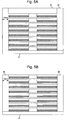
- FIG. 8B shows the top view of the patterned photoresist with the underlying portions of the vertical pillar conductors exposed.
- FIG. 8C is the side cross sectional view of the device stack along the X direction (line X-X′ in FIG. 8B ), while FIG. 8D is the side cross sectional view of the device stack along the Y direction (line Y-Y′ in FIG. 8B ). As shown in FIG.
- the APF 81 , DARC 83 and 193 nm photoresist 85 layers are formed over the device stack 41 and are then exposed and patterned as shown in FIGS. 8B and 8D .
- the spacing between the photoresist patterns may be about 45 to about 100 nm half pitch and the aspect ratio may be about 9:1.
- the exposed portions of the vertical pillar conductors are then etched to form column shaped word lines separated from each other in the Y direction. Each column shaped word line contacts a particular vertical column of diodes. It should be noted that word lines and bit lines may be reversed such that the horizontal conductors act as word lines and the vertical conductors act as bit lines.
- an insulating layer 87 such as silicon oxide or other insulating material is formed over the device stack. Then, as shown in FIG. 9A , this insulating layer is pattered by photolithography, such as 100 nm deep UV (DUV) photolithography, and etching to form openings 91 to the word lines 89 . As shown in FIG. 9B , word line contacts 93 , such as TiN and W contacts are formed in the openings to contact the word lines. As shown in FIG. 9C , the word line contacts are planarized by any suitable method, such as CMP, with the insulating layer 87 acting as a polish stop. The word line contacts remain in the openings after the planarization step. This completes the device.
- photolithography such as 100 nm deep UV (DUV) photolithography
- DUV deep UV
- word line contacts 93 such as TiN and W contacts are formed in the openings to contact the word lines.
- the word line contacts are planarized by any suitable method, such as CMP,
- the stack may be annealed at any suitable point in the process to react the semiconductor layers, such as silicon layers, with the adjacent conductors, such as the word and bit lines to form a silicide layer at the interface.
- the semiconductor layers comprise polysilicon or amorphous silicon and the word and bit lines contain a Ti layer adjacent to the semiconductor layers, a titanium silicide layer is formed at the interface of the semiconductor layers and the adjacent lines.
- first silicide regions are located between the first conductivity type regions 11 in the first 3 and the second 23 semiconductor layers and the respective first and second horizontal conductors 15 , 35 (i.e., bit lines), and second silicide regions are located between the second conductivity type regions 51 in the first and the second semiconductor layers and the patterned vertical pillar conductors (i.e., word lines) 89 .
- FIGS. 10A to 10J illustrate an alternative method of making the device.
- This alternative method first proceeds as illustrated in FIGS. 1-4 .
- a gap fill insulating layer 167 is formed over the device stack 41 , as shown in FIG. 10A , instead of forming the at least one vertical pillar conductor by depositing conductive layers 61 , as shown in FIG. 5A , and then patterning layers 61 into the pillar conductors 65 , as shown in FIG. 5B .
- the insulating layer 167 may be an HDP silicon oxide layer or any other suitable insulating layer, as described above.
- the insulating layer 167 is planarized by CMP or etchback to expose the top of the device stack 41 while the insulating layer 167 remains on the sides of the device stack 41 .
- the alternative method proceeds as shown in FIGS. 6A to 7B and as described above to pattern and isolate the diodes in the Y direction. Then, as shown in FIGS. 10C , 10 D, 10 E and 10 F, word line contact holes are formed in the insulating layer 167 instead of patterning the vertical conductors 65 into word lines as shown in FIGS. 8A to 8D .
- FIG. 10C shows the side view of one or more photosensitive layers, such as the APF 181 , DARC 183 and 193 nm photoresist 185 layers, formed over the device stack 41 .
- FIG. 10D shows the top view of the patterned photoresist with the underlying portions of the insulating layer 167 exposed.
- FIG. 10E is the side cross sectional view of the device stack along the X direction (line X-X′ in FIG. 10D ), while FIG. 10F is the side cross sectional view of the device stack along the Y direction (line Y-Y′ in FIG. 10D ).
- the APF 181 , DARC 183 and photoresist 185 layers are exposed and patterned.
- the openings 186 in the photoresist patterns may be about 45 to about 100 nm, such as about 50 nm half pitch and the aspect ratio may be about 9:1.
- the openings 186 may be slightly wider in the X direction than higher in the Y direction to relax alignment requirements, such that the openings 186 may be about 70 nm wide in the X direction and about 50 nm high in the Y direction.
- each column shaped word line opening 188 exposes a particular vertical column of diodes.
- an optional antifuse dielectric layer 95 shown in FIG. 11 may be formed on each exposed sidewall of the diode at this time by thermally oxidizing the exposed sidewalls of each diode.
- the conductive layers 161 are formed over the device stack 41 and in the openings 188 .
- the conductive layers 161 may comprise titanium, titanium nitride and tungsten, similar to the layers 61 shown in FIG. 5A .
- the conductive layer 161 form the vertical pillar conductor portions in the openings 188 in contact with the p-type regions of the diodes.
- the conductive layers 161 are then planarized by CMP or etchback to expose the top of the device stack 41 and to leave the vertical word lines 89 in the openings 188 , as shown in FIG. 10J .
- the alternative process then proceeds as shown in FIGS. 9A-9C to form word line contacts 93 .
- word lines and bit lines may be reversed such that the horizontal conductors act as word lines and the vertical conductors act as bit lines.
- the word lines are formed by patterning conductive pillars and then depositing an insulating layer around the word lines, while in the alternative method, the word lines are formed by forming one or more conductive layers in openings in an insulating layer.
- FIG. 11 One device level of a completed non-volatile memory device is shown in three dimensions in FIG. 11 .
- the above described method reduces the diode feature size and pitch for sub-45 nm lithography.
- fewer lithography steps such as only two immersion lithography steps, are used to form the structure.
- the aspect ratio will be about the same as for a single layer of upright diodes, but the structure etched will be a line instead of a post.
- the non-volatile memory array includes an array of semiconductor diodes 53 (comprised of n-type regions 11 , intrinsic regions 52 and p-type regions 51 ) in which each semiconductor diode is disposed parallel (i.e., horizontally) with respect to the substrate surface 1 .
- each semiconductor diode is disposed parallel (i.e., horizontally) with respect to the substrate surface 1 .
- a p-type semiconductor region and an n-type semiconductor region are substantially equidistant from the substrate surface.
- substantially equidistant includes within its scope a diode located over a non-planar substrate surface, such that some parts of the diode may be slightly farther from the substrate surface than other parts of the diode due to protrusions or recesses in the substrate surface, such as field oxide protrusions or metal or dielectric filled trenches.
- the non-volatile memory array is a monolithic, three dimensional array of semiconductor diodes in which the semiconductor diodes are located in a plurality of device levels which are stacked in a vertical direction with respect to the substrate surface.
- a monolithic three dimensional memory array is one in which multiple memory levels are formed above a single substrate, such as a wafer, with no intervening substrates. The layers forming one memory level are deposited or grown directly over the layers of an existing level or levels.
- stacked memories have been constructed by forming memory levels on separate substrates and adhering the memory levels atop each other, as in Leedy, U.S. Pat. No. 5,915,167, “Three dimensional structure memory.” The substrates may be thinned or removed from the memory levels before bonding, but as the memory levels are initially formed over separate substrates, such memories are not true monolithic three dimensional memory arrays.
- FIG. 11 A portion of one device level of FIG. 9C in an X-Z plane is shown in FIG. 11 .
- each device level there may be a plurality of diodes 53 in the X direction (i.e., right to left in FIGS. 9C and 11 ) and a plurality of diodes 53 in the Y direction (i.e., in and out of the page in FIGS. 9C and 11 ).
- Each diode in the Y direction is connected to a different word line 89 .
- the same bit line 15 contacts all of the diodes 53 in one device level in the Y direction.
- the same word line 89 contacts all of the diodes 53 in a column in a plurality of device levels.
- the resulting circuit schematic is similar to a conventional cross bar array with word lines extending in one direction and the bit lines extending in a perpendicular direction, except that the bit and word lines do not extend in the same plane parallel to the substrate surface.
- the resulting diodes may be about 30 to 50 nm, such as about 40 nm high, about 40 to about 75, such as about 45 nm wide, and about 0.1 to about 1 microns, such as about 0.3 microns long. Other dimensions may also be used, depending on the specific lithography technique.
- At least one pillar conductor such as a word line 89 , is disposed vertically with respect to the substrate surface 1 .
- This word line is electrically connected to one conductivity type regions 51 of the diodes of the array of semiconductor diodes.
- a plurality of horizontal conductors 15 , 35 are disposed horizontally in the plurality of device levels with respect to the substrate surface 1 .
- the bit lines are electrically connected to the other conductivity type regions 11 of the diodes 53 of the array of semiconductor diodes.
- the horizontal conductors extend to a different distance along the substrate surface in a stepped configuration such that a portion of each horizontal conductor is exposed below an adjacent overlying horizontal conductor. Separate electrical connectors contact each exposed portion of each horizontal conductor.
- each non-volatile memory device of the non-volatile memory array includes an optional antifuse dielectric 95 disposed in series with a semiconductor diode, as shown in FIG. 11 .
- the antifuse is breached to write a data bit.
- each non-volatile memory device is made up solely of one semiconductor diode from the array of semiconductor diodes.
- the semiconductor diode is adapted to change resistivity state in response to an external voltage pulse to write or erase a data bit.
- semiconductor diodes described in U.S. Published Application Numbers US 2007/0164309 A1 and US 2007/0072360 A1 which are hereby incorporated by reference in their entirety, can achieve three, four, or more stable resistivity states.
- semiconductor material can be converted from an initial low-resistivity state to a higher-resistivity state; then, upon application of an appropriate electrical pulse, can be returned to a lower-resistivity state.
- semiconductor material can be converted from an initial high-resistivity state to a lower-resistivity state; then, upon application of an appropriate electrical pulse, can be returned to a higher-resistivity state.
- the voltage pulses may be forward and/or reverse bias pulses to switch the diode from the higher to lower and/or from lower to higher resistivity states, respectively.
- These embodiments can be employed independently or combined to form a memory cell which can have two or more data states, and can be one-time-programmable or rewriteable.
Abstract
Description
Claims (12)
Priority Applications (2)
| Application Number | Priority Date | Filing Date | Title |
|---|---|---|---|
| US11/864,532 US7846782B2 (en) | 2007-09-28 | 2007-09-28 | Diode array and method of making thereof |
| US12/949,056 US8268678B2 (en) | 2007-09-28 | 2010-11-18 | Diode array and method of making thereof |
Applications Claiming Priority (1)
| Application Number | Priority Date | Filing Date | Title |
|---|---|---|---|
| US11/864,532 US7846782B2 (en) | 2007-09-28 | 2007-09-28 | Diode array and method of making thereof |
Related Child Applications (1)
| Application Number | Title | Priority Date | Filing Date |
|---|---|---|---|
| US12/949,056 Continuation US8268678B2 (en) | 2007-09-28 | 2010-11-18 | Diode array and method of making thereof |
Publications (2)
| Publication Number | Publication Date |
|---|---|
| US20090085153A1 US20090085153A1 (en) | 2009-04-02 |
| US7846782B2 true US7846782B2 (en) | 2010-12-07 |
Family
ID=40507227
Family Applications (2)
| Application Number | Title | Priority Date | Filing Date |
|---|---|---|---|
| US11/864,532 Expired - Fee Related US7846782B2 (en) | 2007-09-28 | 2007-09-28 | Diode array and method of making thereof |
| US12/949,056 Active 2027-10-13 US8268678B2 (en) | 2007-09-28 | 2010-11-18 | Diode array and method of making thereof |
Family Applications After (1)
| Application Number | Title | Priority Date | Filing Date |
|---|---|---|---|
| US12/949,056 Active 2027-10-13 US8268678B2 (en) | 2007-09-28 | 2010-11-18 | Diode array and method of making thereof |
Country Status (1)
| Country | Link |
|---|---|
| US (2) | US7846782B2 (en) |
Cited By (13)
| Publication number | Priority date | Publication date | Assignee | Title |
|---|---|---|---|---|
| US8951814B2 (en) | 2004-02-27 | 2015-02-10 | Nvidia Corporation | Method of fabricating a flip chip semiconductor die with internal signal access |
| US9230905B2 (en) | 2014-01-08 | 2016-01-05 | Sandisk 3D Llc | Trench multilevel contact to a 3D memory array and method of making thereof |
| US9331088B2 (en) | 2014-03-25 | 2016-05-03 | Sandisk 3D Llc | Transistor device with gate bottom isolation and method of making thereof |
| US9343507B2 (en) | 2014-03-12 | 2016-05-17 | Sandisk 3D Llc | Dual channel vertical field effect transistor including an embedded electrode |
| US9356043B1 (en) | 2015-06-22 | 2016-05-31 | Sandisk Technologies Inc. | Three-dimensional memory devices containing memory stack structures with position-independent threshold voltage |
| US9419058B1 (en) | 2015-02-05 | 2016-08-16 | Sandisk Technologies Llc | Memory device with comb-shaped electrode having a plurality of electrode fingers and method of making thereof |
| US9583539B2 (en) | 2014-08-19 | 2017-02-28 | Sandisk Technologies Llc | Word line connection for memory device and method of making thereof |
| US9583615B2 (en) | 2015-02-17 | 2017-02-28 | Sandisk Technologies Llc | Vertical transistor and local interconnect structure |
| US9666281B2 (en) | 2015-05-08 | 2017-05-30 | Sandisk Technologies Llc | Three-dimensional P-I-N memory device and method reading thereof using hole current detection |
| US9698202B2 (en) | 2015-03-02 | 2017-07-04 | Sandisk Technologies Llc | Parallel bit line three-dimensional resistive random access memory |
| US9748266B1 (en) | 2016-07-20 | 2017-08-29 | Sandisk Technologies Llc | Three-dimensional memory device with select transistor having charge trapping gate dielectric layer and methods of making and operating thereof |
| US10032908B1 (en) | 2017-01-06 | 2018-07-24 | Sandisk Technologies Llc | Multi-gate vertical field effect transistor with channel strips laterally confined by gate dielectric layers, and method of making thereof |
| US10074661B2 (en) | 2015-05-08 | 2018-09-11 | Sandisk Technologies Llc | Three-dimensional junction memory device and method reading thereof using hole current detection |
Families Citing this family (18)
| Publication number | Priority date | Publication date | Assignee | Title |
|---|---|---|---|---|
| WO2008134828A2 (en) * | 2007-05-04 | 2008-11-13 | Katholieke Universiteit Leuven | Tissue degeneration protection |
| US7846782B2 (en) | 2007-09-28 | 2010-12-07 | Sandisk 3D Llc | Diode array and method of making thereof |
| US7732235B2 (en) * | 2008-06-30 | 2010-06-08 | Sandisk 3D Llc | Method for fabricating high density pillar structures by double patterning using positive photoresist |
| US8114765B2 (en) | 2008-12-31 | 2012-02-14 | Sandisk 3D Llc | Methods for increased array feature density |
| US8084347B2 (en) | 2008-12-31 | 2011-12-27 | Sandisk 3D Llc | Resist feature and removable spacer pitch doubling patterning method for pillar structures |
| US8199576B2 (en) * | 2009-04-08 | 2012-06-12 | Sandisk 3D Llc | Three-dimensional array of re-programmable non-volatile memory elements having vertical bit lines and a double-global-bit-line architecture |
| US8351236B2 (en) | 2009-04-08 | 2013-01-08 | Sandisk 3D Llc | Three-dimensional array of re-programmable non-volatile memory elements having vertical bit lines and a single-sided word line architecture |
| US7983065B2 (en) * | 2009-04-08 | 2011-07-19 | Sandisk 3D Llc | Three-dimensional array of re-programmable non-volatile memory elements having vertical bit lines |
| US8461566B2 (en) | 2009-11-02 | 2013-06-11 | Micron Technology, Inc. | Methods, structures and devices for increasing memory density |
| US8149607B2 (en) * | 2009-12-21 | 2012-04-03 | Sandisk 3D Llc | Rewritable memory device with multi-level, write-once memory cells |
| US8526237B2 (en) | 2010-06-08 | 2013-09-03 | Sandisk 3D Llc | Non-volatile memory having 3D array of read/write elements and read/write circuits and method thereof |
| US8547720B2 (en) | 2010-06-08 | 2013-10-01 | Sandisk 3D Llc | Non-volatile memory having 3D array of read/write elements with efficient decoding of vertical bit lines and word lines |
| CN103377993B (en) * | 2012-04-24 | 2015-06-03 | 中芯国际集成电路制造(上海)有限公司 | Method for forming hole |
| US9349880B2 (en) | 2014-06-17 | 2016-05-24 | Globalfoundries Inc. | Semiconductor devices with semiconductor bodies having interleaved horizontal portions and method of forming the devices |
| US8916872B1 (en) | 2014-07-11 | 2014-12-23 | Inoso, Llc | Method of forming a stacked low temperature diode and related devices |
| US9087689B1 (en) | 2014-07-11 | 2015-07-21 | Inoso, Llc | Method of forming a stacked low temperature transistor and related devices |
| US9524982B2 (en) * | 2015-03-09 | 2016-12-20 | Kabushiki Kaisha Toshiba | Semiconductor device |
| US10833146B2 (en) * | 2019-03-29 | 2020-11-10 | International Business Machines Corporation | Horizontal-trench capacitor |
Citations (48)
| Publication number | Priority date | Publication date | Assignee | Title |
|---|---|---|---|---|
| US4646266A (en) | 1984-09-28 | 1987-02-24 | Energy Conversion Devices, Inc. | Programmable semiconductor structures and methods for using the same |
| US4665428A (en) | 1984-01-13 | 1987-05-12 | The British Petroleum Company P.L.C. | Semiconductor device |
| US5432729A (en) | 1993-04-23 | 1995-07-11 | Irvine Sensors Corporation | Electronic module comprising a stack of IC chips each interacting with an IC chip secured to the stack |
| US5559732A (en) | 1994-12-27 | 1996-09-24 | Syracuse University | Branched photocycle optical memory device |
| US5693556A (en) | 1995-12-29 | 1997-12-02 | Cypress Semiconductor Corp. | Method of making an antifuse metal post structure |
| US5745407A (en) | 1994-05-05 | 1998-04-28 | California Institute Of Technology | Transistorless, multistable current-mode memory cells and memory arrays and methods of reading and writing to the same |
| US5751012A (en) | 1995-06-07 | 1998-05-12 | Micron Technology, Inc. | Polysilicon pillar diode for use in a non-volatile memory cell |
| US5835396A (en) | 1996-10-17 | 1998-11-10 | Zhang; Guobiao | Three-dimensional read-only memory |
| US5915167A (en) | 1997-04-04 | 1999-06-22 | Elm Technology Corporation | Three dimensional structure memory |
| US5962911A (en) | 1996-04-29 | 1999-10-05 | Vlsi Technology, Inc. | Semiconductor devices having amorphous silicon antifuse structures |
| US5991193A (en) | 1997-12-02 | 1999-11-23 | International Business Machines Corporation | Voltage biasing for magnetic ram with magnetic tunnel memory cells |
| US6034882A (en) | 1998-11-16 | 2000-03-07 | Matrix Semiconductor, Inc. | Vertically stacked field programmable nonvolatile memory and method of fabrication |
| US6111784A (en) | 1997-09-18 | 2000-08-29 | Canon Kabushiki Kaisha | Magnetic thin film memory element utilizing GMR effect, and recording/reproduction method using such memory element |
| US6236587B1 (en) | 1997-09-01 | 2001-05-22 | Thin Film Electronics Asa | Read-only memory and read-only memory devices |
| US6306718B1 (en) | 2000-04-26 | 2001-10-23 | Dallas Semiconductor Corporation | Method of making polysilicon resistor having adjustable temperature coefficients |
| US6420215B1 (en) | 2000-04-28 | 2002-07-16 | Matrix Semiconductor, Inc. | Three-dimensional memory array and method of fabrication |
| US6462388B1 (en) * | 2001-07-26 | 2002-10-08 | Hewlett-Packard Company | Isolation of memory cells in cross point arrays |
| US6483736B2 (en) | 1998-11-16 | 2002-11-19 | Matrix Semiconductor, Inc. | Vertically stacked field programmable nonvolatile memory and method of fabrication |
| US6486065B2 (en) | 2000-12-22 | 2002-11-26 | Matrix Semiconductor, Inc. | Method of forming nonvolatile memory device utilizing a hard mask |
| US20030001230A1 (en) | 2000-06-30 | 2003-01-02 | Lowrey Tyler A. | Three dimensional programmable device and method for fabricating the same |
| US6525953B1 (en) | 2001-08-13 | 2003-02-25 | Matrix Semiconductor, Inc. | Vertically-stacked, field-programmable, nonvolatile memory and method of fabrication |
| US6541312B2 (en) | 2000-12-22 | 2003-04-01 | Matrix Semiconductor, Inc. | Formation of antifuse structure in a three dimensional memory |
| US6567301B2 (en) | 2001-08-09 | 2003-05-20 | Hewlett-Packard Development Company, L.P. | One-time programmable unit memory cell based on vertically oriented fuse and diode and one-time programmable memory using the same |
| US6584029B2 (en) | 2001-08-09 | 2003-06-24 | Hewlett-Packard Development Company, L.P. | One-time programmable memory using fuse/anti-fuse and vertically oriented fuse unit memory cells |
| US20030173643A1 (en) * | 2002-03-13 | 2003-09-18 | Matrix Semiconductor, Inc. | Silicide-silicon oxide-semiconductor antifuse device and method of making |
| US6677220B2 (en) | 2002-01-16 | 2004-01-13 | Hewlett-Packard Development Company, L.P. | Antifuse structure and method of making |
| US20040016991A1 (en) | 2000-04-28 | 2004-01-29 | Matrix Semiconductor, Inc. | Silicon nitride antifuse for use in diode-antifuse memory arrays |
| US6693823B2 (en) | 2002-01-02 | 2004-02-17 | Intel Corporation | Minimization of metal migration in magnetic random access memory |
| WO2004055827A1 (en) | 2002-12-13 | 2004-07-01 | Ovonyx, Inc. | Method and system to store information |
| US6777773B2 (en) | 2000-08-14 | 2004-08-17 | Matrix Semiconductor, Inc. | Memory cell with antifuse layer formed at diode junction |
| EP1450373A1 (en) | 2003-02-21 | 2004-08-25 | STMicroelectronics S.r.l. | Phase change memory device |
| US20040228159A1 (en) | 2003-05-13 | 2004-11-18 | Kostylev Sergey A. | Method of eliminating drift in phase-change memory |
| US20040232509A1 (en) | 2003-05-19 | 2004-11-25 | Matrix Semiconductor, Inc. | Rail schottky device and method of making |
| US20050052915A1 (en) | 2002-12-19 | 2005-03-10 | Matrix Semiconductor, Inc. | Nonvolatile memory cell without a dielectric antifuse having high- and low-impedance states |
| US6881994B2 (en) | 2000-08-14 | 2005-04-19 | Matrix Semiconductor, Inc. | Monolithic three dimensional array of charge storage devices containing a planarized surface |
| US20050098800A1 (en) | 2002-12-19 | 2005-05-12 | Matrix Semiconductor, Inc. | Nonvolatile memory cell comprising a reduced height vertical diode |
| US20050121742A1 (en) | 2003-12-03 | 2005-06-09 | Matrix Semiconductor, Inc | Semiconductor device including junction diode contacting contact-antifuse unit comprising silicide |
| US20050158950A1 (en) | 2002-12-19 | 2005-07-21 | Matrix Semiconductor, Inc. | Non-volatile memory cell comprising a dielectric layer and a phase change material in series |
| US6952030B2 (en) | 2002-12-19 | 2005-10-04 | Matrix Semiconductor, Inc. | High-density three-dimensional memory cell |
| US6951780B1 (en) | 2003-12-18 | 2005-10-04 | Matrix Semiconductor, Inc. | Selective oxidation of silicon in diode, TFT, and monolithic three dimensional memory arrays |
| US6952043B2 (en) | 2002-06-27 | 2005-10-04 | Matrix Semiconductor, Inc. | Electrically isolated pillars in active devices |
| US7038248B2 (en) | 2002-02-15 | 2006-05-02 | Sandisk Corporation | Diverse band gap energy level semiconductor device |
| US20060250836A1 (en) | 2005-05-09 | 2006-11-09 | Matrix Semiconductor, Inc. | Rewriteable memory cell comprising a diode and a resistance-switching material |
| US20060250837A1 (en) | 2005-05-09 | 2006-11-09 | Sandisk 3D, Llc | Nonvolatile memory cell comprising a diode and a resistance-switching material |
| US7176064B2 (en) | 2003-12-03 | 2007-02-13 | Sandisk 3D Llc | Memory cell comprising a semiconductor junction diode crystallized adjacent to a silicide |
| US20070072360A1 (en) | 2005-09-28 | 2007-03-29 | Tanmay Kumar | Method for using a memory cell comprising switchable semiconductor memory element with trimmable resistance |
| US20070114509A1 (en) | 2005-11-23 | 2007-05-24 | Sandisk 3D Llc | Memory cell comprising nickel-cobalt oxide switching element |
| US20070164309A1 (en) * | 2002-12-19 | 2007-07-19 | Sandisk 3D Llc | Method of making a diode read/write memory cell in a programmed state |
Family Cites Families (2)
| Publication number | Priority date | Publication date | Assignee | Title |
|---|---|---|---|---|
| US7800932B2 (en) * | 2005-09-28 | 2010-09-21 | Sandisk 3D Llc | Memory cell comprising switchable semiconductor memory element with trimmable resistance |
| US7846782B2 (en) | 2007-09-28 | 2010-12-07 | Sandisk 3D Llc | Diode array and method of making thereof |
-
2007
- 2007-09-28 US US11/864,532 patent/US7846782B2/en not_active Expired - Fee Related
-
2010
- 2010-11-18 US US12/949,056 patent/US8268678B2/en active Active
Patent Citations (49)
| Publication number | Priority date | Publication date | Assignee | Title |
|---|---|---|---|---|
| US4665428A (en) | 1984-01-13 | 1987-05-12 | The British Petroleum Company P.L.C. | Semiconductor device |
| US4646266A (en) | 1984-09-28 | 1987-02-24 | Energy Conversion Devices, Inc. | Programmable semiconductor structures and methods for using the same |
| US5432729A (en) | 1993-04-23 | 1995-07-11 | Irvine Sensors Corporation | Electronic module comprising a stack of IC chips each interacting with an IC chip secured to the stack |
| US5745407A (en) | 1994-05-05 | 1998-04-28 | California Institute Of Technology | Transistorless, multistable current-mode memory cells and memory arrays and methods of reading and writing to the same |
| US5559732A (en) | 1994-12-27 | 1996-09-24 | Syracuse University | Branched photocycle optical memory device |
| US5751012A (en) | 1995-06-07 | 1998-05-12 | Micron Technology, Inc. | Polysilicon pillar diode for use in a non-volatile memory cell |
| US5693556A (en) | 1995-12-29 | 1997-12-02 | Cypress Semiconductor Corp. | Method of making an antifuse metal post structure |
| US5962911A (en) | 1996-04-29 | 1999-10-05 | Vlsi Technology, Inc. | Semiconductor devices having amorphous silicon antifuse structures |
| US5835396A (en) | 1996-10-17 | 1998-11-10 | Zhang; Guobiao | Three-dimensional read-only memory |
| US5915167A (en) | 1997-04-04 | 1999-06-22 | Elm Technology Corporation | Three dimensional structure memory |
| US6236587B1 (en) | 1997-09-01 | 2001-05-22 | Thin Film Electronics Asa | Read-only memory and read-only memory devices |
| US6111784A (en) | 1997-09-18 | 2000-08-29 | Canon Kabushiki Kaisha | Magnetic thin film memory element utilizing GMR effect, and recording/reproduction method using such memory element |
| US5991193A (en) | 1997-12-02 | 1999-11-23 | International Business Machines Corporation | Voltage biasing for magnetic ram with magnetic tunnel memory cells |
| US6483736B2 (en) | 1998-11-16 | 2002-11-19 | Matrix Semiconductor, Inc. | Vertically stacked field programmable nonvolatile memory and method of fabrication |
| US6034882A (en) | 1998-11-16 | 2000-03-07 | Matrix Semiconductor, Inc. | Vertically stacked field programmable nonvolatile memory and method of fabrication |
| US6306718B1 (en) | 2000-04-26 | 2001-10-23 | Dallas Semiconductor Corporation | Method of making polysilicon resistor having adjustable temperature coefficients |
| US6420215B1 (en) | 2000-04-28 | 2002-07-16 | Matrix Semiconductor, Inc. | Three-dimensional memory array and method of fabrication |
| US20040016991A1 (en) | 2000-04-28 | 2004-01-29 | Matrix Semiconductor, Inc. | Silicon nitride antifuse for use in diode-antifuse memory arrays |
| US20030001230A1 (en) | 2000-06-30 | 2003-01-02 | Lowrey Tyler A. | Three dimensional programmable device and method for fabricating the same |
| US6881994B2 (en) | 2000-08-14 | 2005-04-19 | Matrix Semiconductor, Inc. | Monolithic three dimensional array of charge storage devices containing a planarized surface |
| US6777773B2 (en) | 2000-08-14 | 2004-08-17 | Matrix Semiconductor, Inc. | Memory cell with antifuse layer formed at diode junction |
| US6486065B2 (en) | 2000-12-22 | 2002-11-26 | Matrix Semiconductor, Inc. | Method of forming nonvolatile memory device utilizing a hard mask |
| US6541312B2 (en) | 2000-12-22 | 2003-04-01 | Matrix Semiconductor, Inc. | Formation of antifuse structure in a three dimensional memory |
| US6462388B1 (en) * | 2001-07-26 | 2002-10-08 | Hewlett-Packard Company | Isolation of memory cells in cross point arrays |
| US6567301B2 (en) | 2001-08-09 | 2003-05-20 | Hewlett-Packard Development Company, L.P. | One-time programmable unit memory cell based on vertically oriented fuse and diode and one-time programmable memory using the same |
| US6584029B2 (en) | 2001-08-09 | 2003-06-24 | Hewlett-Packard Development Company, L.P. | One-time programmable memory using fuse/anti-fuse and vertically oriented fuse unit memory cells |
| US6525953B1 (en) | 2001-08-13 | 2003-02-25 | Matrix Semiconductor, Inc. | Vertically-stacked, field-programmable, nonvolatile memory and method of fabrication |
| US6693823B2 (en) | 2002-01-02 | 2004-02-17 | Intel Corporation | Minimization of metal migration in magnetic random access memory |
| US6677220B2 (en) | 2002-01-16 | 2004-01-13 | Hewlett-Packard Development Company, L.P. | Antifuse structure and method of making |
| US7038248B2 (en) | 2002-02-15 | 2006-05-02 | Sandisk Corporation | Diverse band gap energy level semiconductor device |
| US20030173643A1 (en) * | 2002-03-13 | 2003-09-18 | Matrix Semiconductor, Inc. | Silicide-silicon oxide-semiconductor antifuse device and method of making |
| US6952043B2 (en) | 2002-06-27 | 2005-10-04 | Matrix Semiconductor, Inc. | Electrically isolated pillars in active devices |
| WO2004055827A1 (en) | 2002-12-13 | 2004-07-01 | Ovonyx, Inc. | Method and system to store information |
| US6952030B2 (en) | 2002-12-19 | 2005-10-04 | Matrix Semiconductor, Inc. | High-density three-dimensional memory cell |
| US20050098800A1 (en) | 2002-12-19 | 2005-05-12 | Matrix Semiconductor, Inc. | Nonvolatile memory cell comprising a reduced height vertical diode |
| US20050158950A1 (en) | 2002-12-19 | 2005-07-21 | Matrix Semiconductor, Inc. | Non-volatile memory cell comprising a dielectric layer and a phase change material in series |
| US20050052915A1 (en) | 2002-12-19 | 2005-03-10 | Matrix Semiconductor, Inc. | Nonvolatile memory cell without a dielectric antifuse having high- and low-impedance states |
| US20070164309A1 (en) * | 2002-12-19 | 2007-07-19 | Sandisk 3D Llc | Method of making a diode read/write memory cell in a programmed state |
| EP1450373A1 (en) | 2003-02-21 | 2004-08-25 | STMicroelectronics S.r.l. | Phase change memory device |
| US20040228159A1 (en) | 2003-05-13 | 2004-11-18 | Kostylev Sergey A. | Method of eliminating drift in phase-change memory |
| US20040232509A1 (en) | 2003-05-19 | 2004-11-25 | Matrix Semiconductor, Inc. | Rail schottky device and method of making |
| US7176064B2 (en) | 2003-12-03 | 2007-02-13 | Sandisk 3D Llc | Memory cell comprising a semiconductor junction diode crystallized adjacent to a silicide |
| US20050121742A1 (en) | 2003-12-03 | 2005-06-09 | Matrix Semiconductor, Inc | Semiconductor device including junction diode contacting contact-antifuse unit comprising silicide |
| US6946719B2 (en) | 2003-12-03 | 2005-09-20 | Matrix Semiconductor, Inc | Semiconductor device including junction diode contacting contact-antifuse unit comprising silicide |
| US6951780B1 (en) | 2003-12-18 | 2005-10-04 | Matrix Semiconductor, Inc. | Selective oxidation of silicon in diode, TFT, and monolithic three dimensional memory arrays |
| US20060250837A1 (en) | 2005-05-09 | 2006-11-09 | Sandisk 3D, Llc | Nonvolatile memory cell comprising a diode and a resistance-switching material |
| US20060250836A1 (en) | 2005-05-09 | 2006-11-09 | Matrix Semiconductor, Inc. | Rewriteable memory cell comprising a diode and a resistance-switching material |
| US20070072360A1 (en) | 2005-09-28 | 2007-03-29 | Tanmay Kumar | Method for using a memory cell comprising switchable semiconductor memory element with trimmable resistance |
| US20070114509A1 (en) | 2005-11-23 | 2007-05-24 | Sandisk 3D Llc | Memory cell comprising nickel-cobalt oxide switching element |
Non-Patent Citations (24)
| Title |
|---|
| Alavi et al, "A PROM Element Based on Salicide Agglomeration of Poly Fuses in a CMOS Logic Process", IEDM 1997. |
| Amemiya et al., "Electrical Trimming of Heavily Doped Polycrystalline Silicon Resistors", IEEE Transactions Electron Devices, vol. ED-26, No. 11, Nov. 1979. |
| Babcock, J. A. et al., "Polysilicon Resistor Trimming for Packaged Integrated Circuits", IEDM 93, 1993, pp. 247-250. |
| Babcock, J. A. et al., "Precision Electrical Trimming of Very Low TCR Poly-Sige Resistors," IEEE Service Center, vol. 21, No. 6, Jun. 2000, pp. 283-285, abstract Figs. 2, 4. |
| Das, Soumen et al., "Electrical Trimming of Ion-Beam-Sputtered Polysilicon Resistors by High Current Pulses", IEEE Transaction of Electron Devices, vol. 41, No. 8, pp. 1429-1434, Aug. 1994. |
| Feldbaumer, D. W. et al., "Theory and Application of Polysilicon Resistor Trimming", Solid-State Electronics, vol. 38, No. 11, 1995, pp. 1861-1869. |
| Feldbaumer, D.W., "Pulse Current Trimming of Polysilicon Resistors", IEEE Transactions on Electron Devices, vol. 42, No. 4, pp. 689-696, Apr. 1995. |
| Kato, Kotaro el al., "A Monolithic 14 Bit D/A Converter Fabricated with a New Trimming Technique (DOT)", IEEE Journal of Solid-State Circuits, vol. SC-19, No. 5, pp. 802-804-806, Oct. 1984. |
| Kato, Kotaro el al., "A Physical Mechanism of Current-Induced Resistance Decrease in Heavily Doped Polysilicon Resistors", IEEE Transaction on Electron Devices, vol. ED-29, No. 8, pp. 1156-1160, Aug. 1982. |
| Kato, Kotaro et al., "Change in Temperature Coefficient of Resistance of Heavily Doped Polysilicon Resistors Caused by Electrical Trimming", Jpn. J. Appl. Phys., vol. 35, Part 1, No. 8, pp. 14209-4215, Aug. 1996. |
| Lane, William A., "The Design of Thin-Film Polysilicon Resistors for Analog IC Applications", IEEE Transactions on Electron Devices, vol. 36, No. 4, pp. 738-744, Apr. 1989. |
| Tobita, Toshio, "New Trimming Technology of a Thick Film Resistor by the Pulse Voltage Method", IEEE Transactions on Components, Hybrids and Manufacturing Technology, vol. 14, No. 3, pp. 613-617, Sep. 1991. |
| U.S. Appl. No. 10/095,962, filed Mar. 13, 2002, Herner et al. |
| U.S. Appl. No. 10/185,507, filed Jun. 27, 2002, Vyvoda et al. |
| U.S. Appl. No. 10/440,882, filed May 19, 2003, Vyvoda et al. |
| U.S. Appl. No. 10/728,436, filed Dec. 5, 2003, Chen. |
| U.S. Appl. No. 10/728,451, filed Dec. 5, 2003, Cleeves et al. |
| U.S. Appl. No. 10/815,312, filed Apr. 1, 2004, Chen. |
| U.S. Appl. No. 10/883,417, filed Jun. 30, 2004, Raghuram et al. |
| U.S. Appl. No. 10/954,510, filed Sep. 29, 2004, Herner. |
| U.S. Appl. No. 11/148,530, filed Jun. 8, 2006, Herner et al. |
| U.S. Appl. No. 11/395,995, filed Mar. 31, 2006, Herner et al. |
| U.S. Appl. No. 11/444,936, May 31, 2006, filed May 31, 2006, Radigan et al. |
| U.S. Appl. No. 11/693,858, Mar. 30, 2007, Kumar et al. |
Cited By (13)
| Publication number | Priority date | Publication date | Assignee | Title |
|---|---|---|---|---|
| US8951814B2 (en) | 2004-02-27 | 2015-02-10 | Nvidia Corporation | Method of fabricating a flip chip semiconductor die with internal signal access |
| US9230905B2 (en) | 2014-01-08 | 2016-01-05 | Sandisk 3D Llc | Trench multilevel contact to a 3D memory array and method of making thereof |
| US9343507B2 (en) | 2014-03-12 | 2016-05-17 | Sandisk 3D Llc | Dual channel vertical field effect transistor including an embedded electrode |
| US9331088B2 (en) | 2014-03-25 | 2016-05-03 | Sandisk 3D Llc | Transistor device with gate bottom isolation and method of making thereof |
| US9583539B2 (en) | 2014-08-19 | 2017-02-28 | Sandisk Technologies Llc | Word line connection for memory device and method of making thereof |
| US9419058B1 (en) | 2015-02-05 | 2016-08-16 | Sandisk Technologies Llc | Memory device with comb-shaped electrode having a plurality of electrode fingers and method of making thereof |
| US9583615B2 (en) | 2015-02-17 | 2017-02-28 | Sandisk Technologies Llc | Vertical transistor and local interconnect structure |
| US9698202B2 (en) | 2015-03-02 | 2017-07-04 | Sandisk Technologies Llc | Parallel bit line three-dimensional resistive random access memory |
| US9666281B2 (en) | 2015-05-08 | 2017-05-30 | Sandisk Technologies Llc | Three-dimensional P-I-N memory device and method reading thereof using hole current detection |
| US10074661B2 (en) | 2015-05-08 | 2018-09-11 | Sandisk Technologies Llc | Three-dimensional junction memory device and method reading thereof using hole current detection |
| US9356043B1 (en) | 2015-06-22 | 2016-05-31 | Sandisk Technologies Inc. | Three-dimensional memory devices containing memory stack structures with position-independent threshold voltage |
| US9748266B1 (en) | 2016-07-20 | 2017-08-29 | Sandisk Technologies Llc | Three-dimensional memory device with select transistor having charge trapping gate dielectric layer and methods of making and operating thereof |
| US10032908B1 (en) | 2017-01-06 | 2018-07-24 | Sandisk Technologies Llc | Multi-gate vertical field effect transistor with channel strips laterally confined by gate dielectric layers, and method of making thereof |
Also Published As
| Publication number | Publication date |
|---|---|
| US20110065243A1 (en) | 2011-03-17 |
| US20090085153A1 (en) | 2009-04-02 |
| US8268678B2 (en) | 2012-09-18 |
Similar Documents
| Publication | Publication Date | Title |
|---|---|---|
| US7846782B2 (en) | Diode array and method of making thereof | |
| USRE46435E1 (en) | Three dimensional hexagonal matrix memory array | |
| US7575984B2 (en) | Conductive hard mask to protect patterned features during trench etch | |
| JP5139269B2 (en) | High density non-volatile memory arrays fabricated at low temperature including semiconductor diodes. | |
| US8187932B2 (en) | Three dimensional horizontal diode non-volatile memory array and method of making thereof | |
| US7285464B2 (en) | Nonvolatile memory cell comprising a reduced height vertical diode | |
| US7001846B2 (en) | High-density SOI cross-point memory array and method for fabricating same | |
| US20080017890A1 (en) | Highly dense monolithic three dimensional memory array and method for forming | |
| US20200194668A1 (en) | Interfacial resistive memory gate stack transistor cell and methods of manufacturing the same | |
| US7887999B2 (en) | Method of making a pillar pattern using triple or quadruple exposure | |
| US20070102724A1 (en) | Vertical diode doped with antimony to avoid or limit dopant diffusion | |
| US8148230B2 (en) | Method of making damascene diodes using selective etching methods | |
| US8076056B2 (en) | Method of making sub-resolution pillar structures using undercutting technique | |
| US20080308856A1 (en) | Integrated Circuit Having a Fin Structure | |
| JP2010532564A (en) | 3D read / write cell with reduced reverse leakage and method of making it |
Legal Events
| Date | Code | Title | Description |
|---|---|---|---|
| AS | Assignment |
Owner name: SANDISK 3D LLC, CALIFORNIA Free format text: ASSIGNMENT OF ASSIGNORS INTEREST;ASSIGNORS:MAXWELL, STEVEN;KONEVECKI, MICHAEL;CLARK, MARK H.;AND OTHERS;REEL/FRAME:019898/0203 Effective date: 20070927 |
|
| STCF | Information on status: patent grant |
Free format text: PATENTED CASE |
|
| FPAY | Fee payment |
Year of fee payment: 4 |
|
| AS | Assignment |
Owner name: SANDISK TECHNOLOGIES INC., TEXAS Free format text: ASSIGNMENT OF ASSIGNORS INTEREST;ASSIGNOR:SANDISK 3D LLC.;REEL/FRAME:038300/0665 Effective date: 20160324 |
|
| AS | Assignment |
Owner name: SANDISK TECHNOLOGIES INC., TEXAS Free format text: CORRECTIVE ASSIGNMENT TO CORRECT THE INCORRECT LISTED PATENT NUMBER 8853569 TO THE CORRECT PATENT NUMBER 8883569 PREVIOUSLY RECORDED ON REEL 038300 FRAME 0665. ASSIGNOR(S) HEREBY CONFIRMS THE ASSIGNMENT;ASSIGNOR:SANDISK 3D LLC;REEL/FRAME:038520/0552 Effective date: 20160324 |
|
| AS | Assignment |
Owner name: SANDISK TECHNOLOGIES LLC, TEXAS Free format text: CHANGE OF NAME;ASSIGNOR:SANDISK TECHNOLOGIES INC;REEL/FRAME:038809/0600 Effective date: 20160516 |
|
| MAFP | Maintenance fee payment |
Free format text: PAYMENT OF MAINTENANCE FEE, 8TH YEAR, LARGE ENTITY (ORIGINAL EVENT CODE: M1552) Year of fee payment: 8 |
|
| FEPP | Fee payment procedure |
Free format text: MAINTENANCE FEE REMINDER MAILED (ORIGINAL EVENT CODE: REM.); ENTITY STATUS OF PATENT OWNER: LARGE ENTITY |
|
| LAPS | Lapse for failure to pay maintenance fees |
Free format text: PATENT EXPIRED FOR FAILURE TO PAY MAINTENANCE FEES (ORIGINAL EVENT CODE: EXP.); ENTITY STATUS OF PATENT OWNER: LARGE ENTITY |
|
| STCH | Information on status: patent discontinuation |
Free format text: PATENT EXPIRED DUE TO NONPAYMENT OF MAINTENANCE FEES UNDER 37 CFR 1.362 |
|
| FP | Lapsed due to failure to pay maintenance fee |
Effective date: 20221207 |