US7858816B2 - Tantalum amido-complexes with chelate ligands useful for CVD and ALD of TaN and Ta205 thin films - Google Patents
Tantalum amido-complexes with chelate ligands useful for CVD and ALD of TaN and Ta205 thin films Download PDFInfo
- Publication number
- US7858816B2 US7858816B2 US12/790,835 US79083510A US7858816B2 US 7858816 B2 US7858816 B2 US 7858816B2 US 79083510 A US79083510 A US 79083510A US 7858816 B2 US7858816 B2 US 7858816B2
- Authority
- US
- United States
- Prior art keywords
- alkyl
- tantalum
- nme
- group
- formula
- Prior art date
- Legal status (The legal status is an assumption and is not a legal conclusion. Google has not performed a legal analysis and makes no representation as to the accuracy of the status listed.)
- Expired - Fee Related
Links
- 0 [1*]N1C(C)N([2*])[Ta]1(C)(C)(C)C Chemical compound [1*]N1C(C)N([2*])[Ta]1(C)(C)(C)C 0.000 description 6
Images


Classifications
-
- C—CHEMISTRY; METALLURGY
- C23—COATING METALLIC MATERIAL; COATING MATERIAL WITH METALLIC MATERIAL; CHEMICAL SURFACE TREATMENT; DIFFUSION TREATMENT OF METALLIC MATERIAL; COATING BY VACUUM EVAPORATION, BY SPUTTERING, BY ION IMPLANTATION OR BY CHEMICAL VAPOUR DEPOSITION, IN GENERAL; INHIBITING CORROSION OF METALLIC MATERIAL OR INCRUSTATION IN GENERAL
- C23C—COATING METALLIC MATERIAL; COATING MATERIAL WITH METALLIC MATERIAL; SURFACE TREATMENT OF METALLIC MATERIAL BY DIFFUSION INTO THE SURFACE, BY CHEMICAL CONVERSION OR SUBSTITUTION; COATING BY VACUUM EVAPORATION, BY SPUTTERING, BY ION IMPLANTATION OR BY CHEMICAL VAPOUR DEPOSITION, IN GENERAL
- C23C16/00—Chemical coating by decomposition of gaseous compounds, without leaving reaction products of surface material in the coating, i.e. chemical vapour deposition [CVD] processes
- C23C16/06—Chemical coating by decomposition of gaseous compounds, without leaving reaction products of surface material in the coating, i.e. chemical vapour deposition [CVD] processes characterised by the deposition of metallic material
- C23C16/18—Chemical coating by decomposition of gaseous compounds, without leaving reaction products of surface material in the coating, i.e. chemical vapour deposition [CVD] processes characterised by the deposition of metallic material from metallo-organic compounds
-
- C—CHEMISTRY; METALLURGY
- C23—COATING METALLIC MATERIAL; COATING MATERIAL WITH METALLIC MATERIAL; CHEMICAL SURFACE TREATMENT; DIFFUSION TREATMENT OF METALLIC MATERIAL; COATING BY VACUUM EVAPORATION, BY SPUTTERING, BY ION IMPLANTATION OR BY CHEMICAL VAPOUR DEPOSITION, IN GENERAL; INHIBITING CORROSION OF METALLIC MATERIAL OR INCRUSTATION IN GENERAL
- C23C—COATING METALLIC MATERIAL; COATING MATERIAL WITH METALLIC MATERIAL; SURFACE TREATMENT OF METALLIC MATERIAL BY DIFFUSION INTO THE SURFACE, BY CHEMICAL CONVERSION OR SUBSTITUTION; COATING BY VACUUM EVAPORATION, BY SPUTTERING, BY ION IMPLANTATION OR BY CHEMICAL VAPOUR DEPOSITION, IN GENERAL
- C23C16/00—Chemical coating by decomposition of gaseous compounds, without leaving reaction products of surface material in the coating, i.e. chemical vapour deposition [CVD] processes
- C23C16/22—Chemical coating by decomposition of gaseous compounds, without leaving reaction products of surface material in the coating, i.e. chemical vapour deposition [CVD] processes characterised by the deposition of inorganic material, other than metallic material
- C23C16/30—Deposition of compounds, mixtures or solid solutions, e.g. borides, carbides, nitrides
- C23C16/34—Nitrides
-
- H—ELECTRICITY
- H01—ELECTRIC ELEMENTS
- H01L—SEMICONDUCTOR DEVICES NOT COVERED BY CLASS H10
- H01L21/00—Processes or apparatus adapted for the manufacture or treatment of semiconductor or solid state devices or of parts thereof
- H01L21/02—Manufacture or treatment of semiconductor devices or of parts thereof
- H01L21/04—Manufacture or treatment of semiconductor devices or of parts thereof the devices having at least one potential-jump barrier or surface barrier, e.g. PN junction, depletion layer or carrier concentration layer
- H01L21/18—Manufacture or treatment of semiconductor devices or of parts thereof the devices having at least one potential-jump barrier or surface barrier, e.g. PN junction, depletion layer or carrier concentration layer the devices having semiconductor bodies comprising elements of Group IV of the Periodic System or AIIIBV compounds with or without impurities, e.g. doping materials
- H01L21/28—Manufacture of electrodes on semiconductor bodies using processes or apparatus not provided for in groups H01L21/20 - H01L21/268
- H01L21/283—Deposition of conductive or insulating materials for electrodes conducting electric current
- H01L21/285—Deposition of conductive or insulating materials for electrodes conducting electric current from a gas or vapour, e.g. condensation
- H01L21/28506—Deposition of conductive or insulating materials for electrodes conducting electric current from a gas or vapour, e.g. condensation of conductive layers
- H01L21/28512—Deposition of conductive or insulating materials for electrodes conducting electric current from a gas or vapour, e.g. condensation of conductive layers on semiconductor bodies comprising elements of Group IV of the Periodic System
- H01L21/28556—Deposition of conductive or insulating materials for electrodes conducting electric current from a gas or vapour, e.g. condensation of conductive layers on semiconductor bodies comprising elements of Group IV of the Periodic System by chemical means, e.g. CVD, LPCVD, PECVD, laser CVD
- H01L21/28562—Selective deposition
-
- H—ELECTRICITY
- H01—ELECTRIC ELEMENTS
- H01L—SEMICONDUCTOR DEVICES NOT COVERED BY CLASS H10
- H01L21/00—Processes or apparatus adapted for the manufacture or treatment of semiconductor or solid state devices or of parts thereof
- H01L21/70—Manufacture or treatment of devices consisting of a plurality of solid state components formed in or on a common substrate or of parts thereof; Manufacture of integrated circuit devices or of parts thereof
- H01L21/71—Manufacture of specific parts of devices defined in group H01L21/70
- H01L21/768—Applying interconnections to be used for carrying current between separate components within a device comprising conductors and dielectrics
- H01L21/76838—Applying interconnections to be used for carrying current between separate components within a device comprising conductors and dielectrics characterised by the formation and the after-treatment of the conductors
- H01L21/76841—Barrier, adhesion or liner layers
- H01L21/76843—Barrier, adhesion or liner layers formed in openings in a dielectric
-
- H—ELECTRICITY
- H01—ELECTRIC ELEMENTS
- H01L—SEMICONDUCTOR DEVICES NOT COVERED BY CLASS H10
- H01L23/00—Details of semiconductor or other solid state devices
- H01L23/52—Arrangements for conducting electric current within the device in operation from one component to another, i.e. interconnections, e.g. wires, lead frames
- H01L23/522—Arrangements for conducting electric current within the device in operation from one component to another, i.e. interconnections, e.g. wires, lead frames including external interconnections consisting of a multilayer structure of conductive and insulating layers inseparably formed on the semiconductor body
- H01L23/532—Arrangements for conducting electric current within the device in operation from one component to another, i.e. interconnections, e.g. wires, lead frames including external interconnections consisting of a multilayer structure of conductive and insulating layers inseparably formed on the semiconductor body characterised by the materials
- H01L23/53204—Conductive materials
- H01L23/53209—Conductive materials based on metals, e.g. alloys, metal silicides
- H01L23/53228—Conductive materials based on metals, e.g. alloys, metal silicides the principal metal being copper
- H01L23/53238—Additional layers associated with copper layers, e.g. adhesion, barrier, cladding layers
-
- H—ELECTRICITY
- H01—ELECTRIC ELEMENTS
- H01L—SEMICONDUCTOR DEVICES NOT COVERED BY CLASS H10
- H01L2924/00—Indexing scheme for arrangements or methods for connecting or disconnecting semiconductor or solid-state bodies as covered by H01L24/00
- H01L2924/0001—Technical content checked by a classifier
- H01L2924/0002—Not covered by any one of groups H01L24/00, H01L24/00 and H01L2224/00
Definitions
- the present invention relates to precursor compositions that are useful for forming tantalum-containing films, e.g., by chemical vapor deposition (CVD) or atomic layer deposition (ALD), as well as to tantalum-containing barrier layers or films and to copper-metallized semiconductor device structures including tantalum-containing layers or films.
- CVD chemical vapor deposition
- ALD atomic layer deposition
- Cu copper
- SiO 2 silicon dioxide
- tantalum (Ta) and tantalum nitrides (TaN) are considered to be among the most promising candidates because of their stability under high temperature, high degree of adhesion, low resistivity, uniformity of their films and their inertness towards Cu.
- vapor deposition techniques e.g., chemical vapor deposition (CVD), atomic layer deposition (ALD), digital CVD, pulsed CVD, or the like, are necessary to deposit the barrier layer, in order to minimize barrier layer thickness while achieving effective barrier properties.
- CVD chemical vapor deposition
- ALD atomic layer deposition
- digital CVD digital CVD
- pulsed CVD pulsed CVD
- CVD chemical vapor deposition
- ALD atomic layer deposition
- suitable tantalum precursors are required for forming tantalum-containing barrier material on substrates.
- Ta amides such as, PDMAT [Ta(NMe 2 ) 5 ], and PEMAT [Ta(NEtMe) 5 ] and Ta imides, such as, TBTDET [t-BuN ⁇ Ta(NEt 2 ) 3 ], and TAIMATA [t-AmN ⁇ Ta(NMe 2 ) 3 ] represent some currently available TaN precursors.
- Thermal stability of amides is problematic.
- PDMAT is a solid with a melting point of 167° C. However, PDMAT decomposes at temperatures above 80° C. PEMAT is a low melting point solid. PEMAT also decomposes at temperatures above 80° C.
- tantalum precursors useful for deposition applications e.g., to form copper migration barrier structures.
- copper migration barrier structures are formed by reactive sputter deposition of a TaN layer onto a patterned, nominally dense dielectric, followed by sputter deposition of Ta metal prior to sputter deposition of a copper seed layer.
- barrier layers e.g., for copper metallization of semiconductor device structures, that do not introduce nitrogen to the underlying dielectric film.
- aspects of various embodiments of the present invention relate generally to precursor compositions for forming tantalum-containing films, as well as to the tantalum-containing films, such as may be employed as barrier layers in semiconductor devices utilizing copper metallization, as well as to semiconductor device structures including tantalum-containing films.
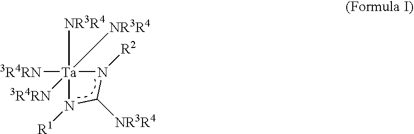
- an embodiment of the present invention relates to a tantalum compound of Formula I:
- R 1 , R 2 , R 3 and R 4 can be the same as or different from one another, and each is independently selected from the group consisting of hydrocarbyl, alkyl, silyl, and, alkylamino.
- R 1 and R 2 cannot both be isopropyl at the same time and/or R 1 and R 2 cannot both be cyclohexyl at the same time.
- One or more embodiments of the invention in another aspect relate to a tantalum precursor formulation, including a tantalum compound (Formulae I) as described above, in a solvent medium.
- a suitable solvent medium is an organic solvent, including but not limited to, hydrocarbon solvents such as pentane, hexane, heptane, octane, decane, THF, ether (e.g., dimethylether (DME)) and aromatic solvents such as toluene.
- hydrocarbon solvents such as pentane, hexane, heptane, octane, decane, THF, ether (e.g., dimethylether (DME)) and aromatic solvents such as toluene.
- DME dimethylether
- embodiments of the invention relate to a method of synthesizing a tantalum compound (Formula I) as described above, in which the method includes conducting synthesis according to Scheme 1 or Scheme 1a below:
- a still further aspect of embodiments of the invention relate to a method of forming a tantalum-containing material on a substrate, including volatilizing a tantalum compound of Formula I as described above, to form a precursor vapor, and depositing tantalum on the substrate from the precursor vapor under deposition conditions therefor.
- the tantalum-containing material on a substrate, the tantalum-containing barrier layer on a substrate, or devices containing same, or methods for making the same may involve (in whole, or in part) the tantalum compounds of Formula I.
- one or more embodiments of the present invention relate to a semiconductor device structure, including a dielectric layer, a barrier layer overlying (or, for example, directly on) the dielectric layer, and a copper metallization overlying (or, for example, directly on) the barrier layer, wherein the barrier layer is optionally amorphous. See, for example, FIG. 5 hereof.
- a still further aspect of one or more embodiments of the invention relates to a method of forming a Ta-containing barrier layer on a dielectric layer which, in turn, is on a substrate.
- the Ta-containing barrier layer may be formed by a process including CVD or ALD using precursors of Formula I as described herein.
- the CVD or ALD is conducted at a temperature below about 400° C., in a reducing atmosphere.
- Yet another aspect of one or more embodiments of the invention relates to a method of inhibiting copper migration in a structure including copper and material adversely affected by copper migration (and/or improving poor adhesion between the copper layer and the barrier layer underneath), comprising interposing a Ta-containing barrier layer between said copper and such material using precursors of Formula I as described herein.
- the CVD or ALD is conducted at a temperature below about 400° C., in a reducing atmosphere (e.g., a suitable nitriding atmosphere such as NH 3 —for example—ammonia gas or ammonia plasma).
- Additional aspects of one or more embodiments of the present invention relate to making a semiconductor device, comprising forming a migration barrier by a vapor deposition process using a vapor deposition precursor including a tantalum compound (Formula I) as described herein, and semiconductor manufacturing methods including use of a tantalum compounds of such type.
- a vapor deposition precursor including a tantalum compound (Formula I) as described herein
- semiconductor manufacturing methods including use of a tantalum compounds of such type.
- the metal source precursors of the invention are volatile and thermally stable, and are usefully employed as precursors for CVD, ALD and/or digital CVD (sometimes referred to as rapid vapor deposition, or RVD) under reduced pressure deposition conditions in corresponding CVD, ALD or digital CVD reactors.
- digital CDV as in ALD, the substrate is sequentially exposed precursors in gaseous form.
- digital CDV the process is repeated until a substrate coated with multiple layers reaches a desired thickness. The resulting coated substrate has a high conformality.
- Digital CVD differs from ALD in that the layers in digital CVD can be deposited more quickly.
- compositions of the present invention can be delivered to the CVD, ALD or digital CVD reactors in a variety of ways.
- a liquid delivery system may be utilized, with the solid precursor(s) being dissolved in organic solvents, and liquid delivery processes being used to meter the solution into a vaporizer for transport of the vapor to the reactor.
- a combined liquid delivery and flash vaporization process unit may be employed, to enable low volatility materials to be volumetrically delivered, so that reproducible transport and deposition are achieved without thermal decomposition of the precursor, in order to provide a commercially acceptable CVD, ALD or digital CVD process.
- a liquid delivery system may be utilized wherein the precursor is stored in and delivered from an ionic liquid.
- metal source precursors that are liquids may be used in neat liquid form, or liquid or solid metal source precursors may be employed in solvent formulations containing same.
- metal source precursor formulations of the invention may include solvent component(s) of suitable character as may be desirable and advantageous in a given end use application to form metals on a substrate.
- Suitable solvents may for example include alkane solvents (e.g., hexane, heptane, octane, nonane, decane and pentane), aryl solvents (e.g., benzene or toluene), amines (e.g., triethylamine, tert-butylamine), imines and carbodiimides (e.g., N,N′-diisopropylcarbodiimide).
- alkane solvents e.g., hexane, heptane, octane, nonane, decane and pentane
- aryl solvents e.g., benzene or toluene
- amines e.g., triethylamine, tert-butylamine
- imines and carbodiimides e.g., N,N′-diisopropylcarbodi
- the solvent utilized in the source reagent solutions of the invention are selected from among aliphatic hydrocarbons, aromatic hydrocarbons, ethers, esters, nitriles, and alcohols.
- the solvent component of the solution can comprise a solvent selected from the group consisting of: glyme solvents having from 1 to 20 ethoxy —(C 2 H 4 O)— repeat units; C 2 -C 12 alkanols, organic ethers selected from the group consisting of dialkyl ethers comprising C 1 -C 6 alkyl moieties, C 4 -C 8 cyclic ethers; C 12 -C 60 -crown-O 4 —O 20 ethers wherein the prefixed C i range is the number i of carbon atoms in the ether compound and the suffixed O i range is the number i of oxygen atoms in the ether compound; C 6 -C 12 aliphatic hydrocarbons; C 6 -C 18 aromatic hydrocarbons; organic esters
- a solid delivery system may be utilized, for example, using the ProE-Vap® solid delivery and vaporizer unit (commercially available from ATMI, Inc., Danbury, Conn., USA).
- a liquid delivery system may be utilized, for example using the NOWTrak® system (commercially available from ATMI, Inc., Danbury, Conn., USA).
- the packaging utilized in liquid delivery employing the NOWTrak® system includes a disposable liner adapted to hold the liquid precursor composition.
- Exemplary systems include, but are not limited to, those set forth in U.S. Pat. No. 6,879,876, filed Jun. 13, 2001 and issued Apr. 12, 2005 and titled “Liquid handling system with electronic information storage”; U.S. patent application Ser. No. 10/139,104, filed May 3, 2002 and titled “Liquid handling system with electronic information storage”; U.S. patent application Ser. No.
- FIG. 1 includes the 1 H & 13 C NMRs of [(Bu t NC(NMe 2 )NEt)Ta(NMe 2 ) 4 ].
- the top plot is the 13 C NMR.
- the bottom plot is the 1 H NMR.
- FIG. 2 is an STA (simultaneous thermal analysis) diagram illustrating comparison of STA data among DEMAT (5.15 mg), [(Bu t NC(NMe 2 )NEt)Ta(NMe 2 ) 4 ] (9.56 mg) and (NMe 2 ) 4 Ta( ⁇ Pr i NC(NMe 2 )NPr i ) (10.57 mg).
- FIG. 3 is an ORTEP diagram of [(Bu t NC(NMe 2 )NEt)Ta(NMe 2 ) 4 ].
- FIG. 4 is a packing diagram of [(Bu t NC(NMe 2 )NEt)Ta(NMe 2 ) 4 ] along the c axis.
- FIG. 5 is a schematic illustration of a semiconductor device structure according to one embodiment of the present invention, featuring an amorphous Ta-containing barrier film and copper metallization.
- One or more embodiments of the present invention relate in various aspects to precursor compositions (and vapor, gas or plasma forms thereof) useful for forming tantalum-containing films (e.g., barrier layers or films).
- Other embodiments relate to tantalum-containing films, such as may be employed as barrier layers in semiconductor devices utilizing copper metallization, as well as to other semiconductor device structures including tantalum-containing films.
- semiconductor device structures is intended to be broadly construed to include microelectronic devices, products, components, assemblies and subassemblies that include a semiconductor material as a functional material therein.
- semiconductor device structures include, without limitation, resist-coated semiconductor substrates, flat-panel displays, thin-film recording heads, microelectromechanical systems (MEMS), and other advanced microelectronic components.
- the semiconductor device structure may include patterned and/or blanketed silicon wafers, flat-panel display substrates or fluoropolymer substrates. Further, the semiconductor device structure may include mesoporous or microporous inorganic solids.
- Alkyls as used herein include, but are not limited to, methyl, ethyl, propyl, isopropyl, butyl, s-butyl, t-butyl, pentyl and isopentyl and the like.
- Aryls as used herein includes hydrocarbons derived from benzene or a benzene derivative that are unsaturated aromatic carbocyclic groups of from 6 to 10 carbon atoms. The aryls may have a single or multiple rings. The term “aryl” as used herein also includes substituted aryls.
- Examples include, but are not limited to phenyl, naphthyl, xylene, phenylethane, substituted phenyl, substituted naphthyl, substituted xylene, substituted phenylethane and the like.
- Cycloalkyls as used herein include, but are not limited to cyclopropyl, cyclobutyl, cyclopentyl, cyclohexyl and the like.
- a range of carbon numbers will be regarded as specifying a sequence of consecutive alternative carbon-containing moieties, including all moieties containing numbers of carbon atoms intermediate the endpoint values of carbon number in the specific range as well as moieties containing numbers of carbon atoms equal to an endpoint value of the specific range, e.g., C 1 -C 6 , is inclusive of C 1 , C 2 , C 3 , C 4 , C 5 and C 6 , and each of such broader ranges may be further limitingly specified with reference to carbon numbers within such ranges, as sub-ranges thereof.
- the range C 1 -C 6 would be inclusive of and can be further limited by specification of sub-ranges such as C 1 -C 3 , C 1 -C 4 , C 2 -C 6 , C 4 -C 6 , etc. within the scope of the broader range.
- film refers to a layer of deposited material having a thickness below 1000 micrometers, e.g., from such value down to atomic monolayer thickness values.
- film thicknesses of deposited material layers in the practice of the invention may for example be below 100, 10, or 1 micrometers, or in various thin film regimes below 200, 100, or 50 nanometers, depending on the specific application involved.
- the term “thin film” means a layer of a material having a thickness below 1 micrometer.
- R 1 , R 2 , R 3 and R 4 can be the same as or different from one another, and each is independently selected from the group consisting of hydrocarbyl, alkyl, silyl, and alkylamino.
- R 1 and R 2 cannot both be isopropyl at the same time and/or R 1 and R 2 cannot both be cyclohexyl at the same time.
- R 1 , R 2 , R 3 and R 4 can be the same as or different from one another, and each is independently selected from hydrocarbyl (e.g., C 1 -C 12 alkyl such as C 1 alkyl (i.e., methyl), C 2 alkyl (i.e., ethyl), C 3 alkyl (e.g., n-propyl or iso-propyl), C 4 alkyl (e.g., n-butyl, iso-butyl, t-butyl), C 5 alkyl (e.g., n-pentyl, iso-pentyl), C 8 alkyl (e.g., octyl), C 9 alkyl (e.g., nonyl), C 10 alkyl, C 11 alkyl, C 12 alkyl), alkenyl (e.g., C 1 -C 12 alkenyl), and ary
- organo substituents by reference to carbon numbers, includes ranges as well as sub-ranges within the ranges identified by end-point carbon numbers, and such sub-ranges may be specified, e.g., as including one of such end-point carbon numbers in such a sub-range, or as including carbon numbers greater than the lower end-point carbon number and less than the upper end-point carbon number of the range, to constitute various sub-ranges in the various specific embodiments of the invention.
- Alkyl groups may be branched or unbranched.
- the precursors of Formula I are useful for forming tantalum-containing films, e.g., involving CVD and ALD of tantalum nitride and Ta metal films. These precursors also have utility as low temperature deposition precursors for forming Ta 2 O 5 and other Ta oxide films, e.g., in the fabrication of capacitors such as back-end capacitors.
- novel complexes may be readily purified, and their solution behavior in solvent media employed for liquid delivery processes, e.g., for CVD or ALD of Ta, TaN or Ta 2 O 5 films is superior to that of PDMAT [Ta(NMe 2 ) 5 ], PEMAT [Ta(NEtMe) 5 ], etc.
- the precursors of Formula I may be usefully employed for deposition of Ta-containing material on substrates, including, without limitation, deposition of Ta, TaN, Ta 2 O 5 , TaSiN, BiTaO 4 , etc.
- the Ta-containing material may be deposited on the substrate in any suitable manner, with deposition processes such as CVD and ALD sometimes being preferred.
- the Formula I precursors may also be deposited by solid delivery techniques, e.g., in which the precursor is volatilized from a solid form under suitable temperature and pressure, e.g., vacuum conditions.
- the CVD process may be carried out in any suitable manner, for example, with the volatilized precursor being conveyed to a CVD reactor for contact with a heated substrate, e.g., a silicon wafer-based structure, or other microelectronic device substrate.
- the volatilized precursor may be directed to the CVD reactor in neat form, or, more typically, in a carrier gas stream, which may include inert gas, plasma, oxidant, reductant, co-deposition species, and/or the like.
- the CVD process may be carried out by liquid delivery processing, for example, in which the Ta precursor is dissolved or suspended in a solvent medium, which may include a single solvent or multi-solvent composition, as appropriate to the specific deposition application involved.
- a solvent medium which may include a single solvent or multi-solvent composition, as appropriate to the specific deposition application involved.
- Suitable solvents for such purpose include any compatible solvents that are consistent with liquid delivery processing, as for example, hydrocarbon solvents, etc., with a suitable solvent for the specific deposition application being readily determinable within the skill of the art based on the disclosure herein.
- the precursors of Formula I have particular utility as CVD or ALD precursors for deposition of thin films of TaN and TaSiN as barriers in integrated circuits, e.g., integrated circuitry including dielectric material and copper metallization.
- the precursors of Formula I may also have particular utility as CVD or ALD precursors for deposition of Ta containing metal films as barriers in integrated circuits.
- R 1 , R 2 , R 3 and R 4 can be the same as or different from one another, and each is independently selected from hydrocarbyl substituents including alkyl, arylalkyl, alkaryl, alkenyl, alkenylaryl, arylalkenyl, allyl, hydrogen, silyl, hydrazyl (for example, Me 2 NNH—) and alkylamino (for example, Me 2 N—, MeHN—, etc.) etc.
- compositions that are optionally further substituted with one or more heteroatoms such as N, S, and O and/or with halo substituents and any combination or sub-combination thereof, and providing functionality that is sterically and chemically appropriate to the use of the composition as a precursor for forming tantalum-containing films and materials—as described herein.
- the precursors of Formula I have utility for CVD and ALD of Ta carbide and Ta metal films, as well as for low temperature deposition of TaN, Ta 2 O 5 and other Ta-related oxide films for use in capacitor fabrication.
- R 1 , R 2 , R 3 , and R 4 are as described herein and M is tantalum.
- the Formula I precursors are thermally stable and stable in solution.
- the R 1 , R 2 , R 3 , and R 4 ligands may be appropriately selected for the specific deposition application employed, e.g., for CVD or ALD deposition processing to form the desired Ta-containing material on the deposition substrate, within the skill of the art—based on the disclosure herein.
- the Formula I precursors are readily purified, and their solution behavior in solvent media may be suitably employed for liquid delivery processes, e.g., for CVD or ALD of Ta, TaN or Ta 2 O 5 films.
- the precursors of Formula I have utility as CVD or ALD precursors for deposition of thin films of TaN and TaSiN as barriers in integrated circuits, e.g., integrated circuitry including dielectric material and copper metallization.
- the precursors of Formula I also have particular utility as CVD or ALD precursors for low temperature deposition of thin films of high k capacitor materials such as Ta 2 O 5 and BiTaO 4 .
- the precursors of Formula I have utility for CVD and ALD of Ta nitride and Ta metal films, as well as for low temperature deposition of Ta 2 O 5 and other Ta-related oxide films for use in capacitor fabrication.
- FIG. 1 shows a 13 C and 1 H NMR plot of. [(Bu t NC(NMe 2 )NEt)Ta(NMe 2 ) 4 ].
- the top plot is the 13 C NMR.
- the bottom plot is the 1 H NMR.
- FIG. 2 is an STA (simultaneous thermal analysis) diagram illustrating comparison of STA data among DEMAT (green line, 5.15 mg), [(Bu t NC(NMe 2 )NEt)Ta(NMe 2 ) 4 ] (blue line, 9.56 mg) and (NMe 2 ) 4 Ta( ⁇ 2-Pr i NC(NMe 2 )NPr i ) (brown line, 10.57 mg).
- Thermal analysis see STA data in FIG. 2 ) showed the material transport completely below 250° C. with a low residue of 1.6% at 800° C.
- FIG. 3 is an ORTEP diagram of [(Bu t NC(NMe 2 )NEt)Ta(NMe 2 ) 4 ]
- FIG. 4 is a packing diagram of [(Bu t NC(NMe 2 )NEt)Ta(NMe 2 ) 4 ] along the c axis.
- FIG. 5 is a schematic illustration of a semiconductor device structure according to one embodiment of the present invention, featuring an amorphous Ta-containing barrier film and copper metallization.
- the precursors of Formula I may be usefully employed for deposition of Ta-containing material on substrates, including, without limitation, deposition of Ta, TaN, Ta 2 O 5 , TaSiN, BiTaO 4 , etc.
- the Ta-containing material may be deposited on the substrate in any suitable manner, for example, with deposition processes such as CVD and ALD sometimes being preferred.
- the Formula I precursors may also be deposited by solid delivery techniques, e.g., in which the precursor is volatilized from a solid form under suitable temperature and pressure, e.g., vacuum conditions.
- the CVD process may be carried out in any suitable manner, with the volatilized precursor being conveyed to a CVD reactor for contact with a heated substrate, e.g., a silicon wafer-based structure, or other microelectronic device substrate.
- the volatilized precursor may be directed to the CVD reactor in neat form, or, more typically, in a carrier gas stream, which may include inert gas, plasma, oxidant, reductant, co-deposition species, or the like.
- the CVD process may be carried out by liquid delivery processing, in which the Ta precursor is dissolved or suspended in a solvent medium, which may include a single solvent or multi-solvent composition, as appropriate to the specific deposition application involved.
- Suitable solvents for such purpose include any compatible solvents that are consistent with liquid delivery processing, as for example, hydrocarbon solvents, etc., with a suitable solvent for a specific deposition application being readily determinable within the skill of the art based on the disclosure herein.
- suitable hydrocarbon solvents include, but are not limited to, pentane, hexane, heptane, octane, decane, cyclohexane, THF, toluene, and DME. Other suitable solvents may be used.
- the precursors of Formula I may have particular utility as CVD or ALD precursors for deposition of thin films of TaN and TaSiN as barriers in integrated circuits, e.g., integrated circuitry including dielectric material and copper metallization.
- the precursors of Formula I may also have particular utility as CVD or ALD precursors for low temperature deposition of thin films of high k capacitor materials such as Ta 2 O 5 and BiTaO 4 .
- the precursors of Formula I may also have particular utility as CVD or ALD precursors for deposition of Ta metal films as barriers in integrated circuits.
- One or more embodiments of the present invention relate to tantalum-containing barrier films, such as may usefully be employed as diffusion barriers in semiconductor devices featuring copper metallization, and reflects the discovery that Ta compounds (Formula I) can be used to efficiently form tantalum-based barrier films at low temperatures under reducing conditions.
- the Ta compounds that can be usefully employed for forming the Ta-containing barrier film may be of any suitable type, including a Ta—NR 1 —C(NR 3 R 4 )—NR 2 (see Formula I and Formula II noted herein containing same) moiety and substituents that permit the Ta-containing barrier film to be formed (in whole or in part)—sometimes preferably as an amorphous structure.
- the Ta compound precursor may be volatilized to form a precursor vapor for CVD or ALD formation of the Ta-containing barrier film.
- the precursor volatilization and delivery to the deposition chamber may be carried out in any suitable manner, e.g., by bubbler delivery involving an inert or reducing carrier gas flow through the bubbler, or by solid delivery technique, in which the precursor is volatilized from a solid form under suitable temperature and pressure, e.g., vacuum conditions involving sublimation of the precursor compound and mixing of the precursor vapor with inert or reducing carrier gas, or by liquid delivery technique in which the precursor is dissolved in a suitable solvent medium, such as hexane, octane, toluene or other organic solvent, with the resulting liquid being flash vaporized to produce the precursor vapor, or by any other appropriate technique that results in the provision of a precursor vapor suitable for contacting with the substrate (the layer to be coated).
- the precursor vapor can contain or be mixed with a reducing agent of appropriate character and concentration to provide a suitable reducing atmosphere in the deposition chamber.
- the substrate on which the barrier film is to be formed is heated to temperature effective for contacting with the precursor vapor to affect the film formation process, and then contacted with the precursor vapor to form the Ta-containing barrier film on the substrate.
- the reducing agent can be hydrogen, hydrogen plasma, remote hydrogen plasma, silane, disilane, borane, diborane, ammonia (gas or plasma), amines (Me 2 NH, t-BuNH 2 , Et 2 NH) or the like, or mixture of two or more of the foregoing species, as satisfactory to provide an atmosphere in the deposition chamber that facilitates the formation of the Ta-containing film.
- the reducing co-reactants may be introduced simultaneously with the Ta precursor or in an alternating manner (i.e., via digital or pulsed CVD or ALD).
- the substrate can be of any appropriate type.
- the substrate includes a silicon wafer having a low k dielectric film thereon, suitably patterned for the deposition of the barrier film to accommodate subsequent copper metallization of the semiconductor device structure formed on the wafer.
- the deposition may be carried out at temperature to form the Ta-containing barrier layer that is appropriate for the specific technique that is employed for the deposition, e.g., CVD, ALD, digital CVD, pulsed CVD, or the like.
- temperature 100° C. or higher, but below 400° C., can be utilized as the deposition temperature.
- the temperature for deposition is below 390° C.
- specific operating regimes for the process include temperatures in a range of from about 250° C. to about 380° C., and temperatures in a range of from about 275° C. to about 350° C. in other embodiments of the invention.
- ALD may for example be carried out at a temperature of about 280° C.
- Pressure may likewise be selected based on volatilization, transport and deposition properties of the specific precursor employed, with vacuum pressures being useful in some applications, e.g., where solid delivery is employed as the delivery technique.
- CVD and ALD pressures may include deposition pressures in a range of from about 0 to about 1000 Pascal, or other pressure appropriate to the particular deposition methodology.
- FIG. 5 is a schematic illustration of a semiconductor device structure 10 according to one embodiment of the present invention, featuring an amorphous Ta-containing barrier film and copper metallization.
- the device structure 10 includes a silicon substrate 12 , on which has been deposited a low k dielectric material 14 .
- An amorphous barrier film 16 is deposited on the dielectric in accordance with an embodiment of the invention, and overlaid with a seed layer 18 of copper or ruthenium, on which is deposited a copper metallization layer 20 .
- the barrier film e.g., Ta-containing film or layer
- the seed layer may be composed of ruthenium or other suitable seed for deposition of copper metallization.
- a precursor compound of Formula I may be used to efficiently and cost-effectively deposit a tantalum-containing film in a reducing atmosphere at low temperature, to produce an amorphous Ta-containing barrier against copper diffusion, in semiconductor device structures featuring copper metallization.
- the invention thereby achieves a significant advance in the art of copper metallization using thermally stable Ta-containing precursors to form corresponding barrier layers in the device structure.
- the R group substituents of tantalum compounds of Formula I hereof can further include variations and derivatives of the chemical moieties specifically identified herein, e.g., in respect of hydrocarbyl substituents including alkyl, arylalkyl, alkaryl, alkenyl, alkenylaryl, arylalkenyl, allyl, hydrogen, silyl, hydrazyl (for example, Me 2 NH—) and alkylamino (for example, Me 2 N—, MeHN—, etc.) etc.
- tantalum composition as a precursor for forming tantalum-containing films and materials.
- the tantalum compositions of the invention can be utilized in solution including any suitable solvents, such as for example hydrocarbon solvents (pentane, hexane, heptane, octane, decane, cyclohexane, etc.), THF, ethers (e.g., DME), toluene and the like, as necessary or desirable in a given application of a specific tantalum composition of the invention.
- suitable solvents such as for example hydrocarbon solvents (pentane, hexane, heptane, octane, decane, cyclohexane, etc.), THF, ethers (e.g., DME), toluene and the like, as necessary or desirable in a given application of a specific tantalum composition of the invention.
Abstract
Description

wherein:
R1, R2, R3 and R4 can be the same as or different from one another, and each is independently selected from the group consisting of hydrocarbyl, alkyl, silyl, and, alkylamino.

where M=Ta.
wherein:
R1, R2, R3 and R4 can be the same as or different from one another, and each is independently selected from the group consisting of hydrocarbyl, alkyl, silyl, and alkylamino. In some embodiments, R1 and R2 cannot both be isopropyl at the same time and/or R1 and R2 cannot both be cyclohexyl at the same time.


In such synthetic schemes, R1, R2, R3, and R4 are as described herein and M is tantalum.
Claims (20)

M(NR3R4)5 (Formula II),
R1N═C═NR2 (Formula III),
Priority Applications (1)
| Application Number | Priority Date | Filing Date | Title |
|---|---|---|---|
| US12/790,835 US7858816B2 (en) | 2007-01-18 | 2010-05-30 | Tantalum amido-complexes with chelate ligands useful for CVD and ALD of TaN and Ta205 thin films |
Applications Claiming Priority (3)
| Application Number | Priority Date | Filing Date | Title |
|---|---|---|---|
| US88545907P | 2007-01-18 | 2007-01-18 | |
| US12/013,433 US7750173B2 (en) | 2007-01-18 | 2008-01-12 | Tantalum amido-complexes with chelate ligands useful for CVD and ALD of TaN and Ta205 thin films |
| US12/790,835 US7858816B2 (en) | 2007-01-18 | 2010-05-30 | Tantalum amido-complexes with chelate ligands useful for CVD and ALD of TaN and Ta205 thin films |
Related Parent Applications (1)
| Application Number | Title | Priority Date | Filing Date |
|---|---|---|---|
| US12/013,433 Division US7750173B2 (en) | 2007-01-18 | 2008-01-12 | Tantalum amido-complexes with chelate ligands useful for CVD and ALD of TaN and Ta205 thin films |
Publications (2)
| Publication Number | Publication Date |
|---|---|
| US20100240918A1 US20100240918A1 (en) | 2010-09-23 |
| US7858816B2 true US7858816B2 (en) | 2010-12-28 |
Family
ID=40337345
Family Applications (2)
| Application Number | Title | Priority Date | Filing Date |
|---|---|---|---|
| US12/013,433 Active 2028-08-03 US7750173B2 (en) | 2007-01-18 | 2008-01-12 | Tantalum amido-complexes with chelate ligands useful for CVD and ALD of TaN and Ta205 thin films |
| US12/790,835 Expired - Fee Related US7858816B2 (en) | 2007-01-18 | 2010-05-30 | Tantalum amido-complexes with chelate ligands useful for CVD and ALD of TaN and Ta205 thin films |
Family Applications Before (1)
| Application Number | Title | Priority Date | Filing Date |
|---|---|---|---|
| US12/013,433 Active 2028-08-03 US7750173B2 (en) | 2007-01-18 | 2008-01-12 | Tantalum amido-complexes with chelate ligands useful for CVD and ALD of TaN and Ta205 thin films |
Country Status (1)
| Country | Link |
|---|---|
| US (2) | US7750173B2 (en) |
Cited By (1)
| Publication number | Priority date | Publication date | Assignee | Title |
|---|---|---|---|---|
| US20170178961A1 (en) * | 2015-12-21 | 2017-06-22 | Adeka Corporation | Tantalum compound and methods of forming thin film and fabricating integrated circuit device by using the same |
Families Citing this family (13)
| Publication number | Priority date | Publication date | Assignee | Title |
|---|---|---|---|---|
| US7323581B1 (en) * | 1990-07-06 | 2008-01-29 | Advanced Technology Materials, Inc. | Source reagent compositions and method for forming metal films on a substrate by chemical vapor deposition |
| US6960675B2 (en) * | 2003-10-14 | 2005-11-01 | Advanced Technology Materials, Inc. | Tantalum amide complexes for depositing tantalum-containing films, and method of making same |
| WO2007133837A2 (en) | 2006-05-12 | 2007-11-22 | Advanced Technology Materials, Inc. | Low temperature deposition of phase change memory materials |
| KR101279925B1 (en) | 2006-11-02 | 2013-07-08 | 어드밴스드 테크놀러지 머티리얼즈, 인코포레이티드 | Antimony and germanium complexes useful for cvd/ald of metal thin films |
| US7750173B2 (en) | 2007-01-18 | 2010-07-06 | Advanced Technology Materials, Inc. | Tantalum amido-complexes with chelate ligands useful for CVD and ALD of TaN and Ta205 thin films |
| US20100209610A1 (en) * | 2007-07-16 | 2010-08-19 | Advanced Technology Materials, Inc. | Group iv complexes as cvd and ald precursors for forming metal-containing thin films |
| US8834968B2 (en) | 2007-10-11 | 2014-09-16 | Samsung Electronics Co., Ltd. | Method of forming phase change material layer using Ge(II) source, and method of fabricating phase change memory device |
| KR101458953B1 (en) | 2007-10-11 | 2014-11-07 | 삼성전자주식회사 | Method of forming phase change material layer using Ge(Ⅱ) source, and method of fabricating phase change memory device |
| US20090215225A1 (en) | 2008-02-24 | 2009-08-27 | Advanced Technology Materials, Inc. | Tellurium compounds useful for deposition of tellurium containing materials |
| US20100062149A1 (en) * | 2008-09-08 | 2010-03-11 | Applied Materials, Inc. | Method for tuning a deposition rate during an atomic layer deposition process |
| US8491967B2 (en) * | 2008-09-08 | 2013-07-23 | Applied Materials, Inc. | In-situ chamber treatment and deposition process |
| TWI508176B (en) | 2011-06-20 | 2015-11-11 | Applied Materials Inc | N-metal film deposition with initiation layer |
| US10186570B2 (en) * | 2013-02-08 | 2019-01-22 | Entegris, Inc. | ALD processes for low leakage current and low equivalent oxide thickness BiTaO films |
Citations (178)
| Publication number | Priority date | Publication date | Assignee | Title |
|---|---|---|---|---|
| US2839421A (en) | 1955-04-06 | 1958-06-17 | Du Pont | An alkoxy aluminum chelate, a dispersion of it in an organic liquid and a water repellant porous object |
| US3076834A (en) | 1960-03-04 | 1963-02-05 | Dow Chemical Co | Chelate-phenol adducts |
| GB976573A (en) | 1959-12-30 | 1964-11-25 | Union Carbide Corp | Improvements in and relating to metal plating |
| US3288829A (en) | 1961-01-19 | 1966-11-29 | Ethyl Corp | Process for preparing cyclopentadienyl group vb and vib metal hydrides |
| US3356527A (en) | 1964-04-23 | 1967-12-05 | Ross W Moshier | Vapor-plating metals from fluorocarbon keto metal compounds |
| US3437516A (en) | 1966-04-28 | 1969-04-08 | Us Air Force | Vapor deposition from perfluoroorganometallic compounds |
| US3467686A (en) | 1967-10-03 | 1969-09-16 | Union Carbide Corp | Preparation of organosilicon-nitrogen compounds |
| US3594216A (en) | 1969-06-19 | 1971-07-20 | Westinghouse Electric Corp | Vapor phase deposition of metal from a metal-organic beta-ketoamine chelate |
| US3988332A (en) | 1974-05-20 | 1976-10-26 | E. I. Du Pont De Nemours And Company | Hydrocarbylidene compounds of niobium and tantalum |
| US4147556A (en) | 1972-01-12 | 1979-04-03 | Ppg Industries, Inc. | Nonflammable beta diketonate composition |
| US4281037A (en) | 1980-08-08 | 1981-07-28 | Dap, Inc. | Cleaning and priming composition containing titanium acetylacetonate and method |
| US4383119A (en) | 1982-06-04 | 1983-05-10 | Chemplex Company | Organomagnesium compounds |
| US4401474A (en) | 1979-12-03 | 1983-08-30 | Ppg Industries, Inc. | Pyrolytic coating reactant for defect and durability control |
| US4491669A (en) | 1980-11-12 | 1985-01-01 | Petrarch Systems Inc. | Mixed alkoxyaminosilanes, methods of making same and vulcanizing silicons prepared therefrom |
| US4499198A (en) | 1982-10-07 | 1985-02-12 | Chemplex Company | Polymerization catalysts and methods |
| US4510222A (en) | 1982-05-24 | 1985-04-09 | Hitachi, Ltd. | Photomask with corrected white defects |
| US4529427A (en) | 1977-05-19 | 1985-07-16 | At&T Bell Laboratories | Method for making low-loss optical waveguides on an industrial scale |
| DE3447635A1 (en) | 1983-12-28 | 1985-07-18 | Hitachi, Ltd., Tokio/Tokyo | METHOD FOR PRODUCING SOLAR CELLS |
| US4726938A (en) | 1985-01-15 | 1988-02-23 | Rhone-Poulenc Specialites Chimiques | Liquid/liquid extraction/purification of impure solutions of rare earth values |
| US4895709A (en) | 1985-04-26 | 1990-01-23 | Sri International | Method of preparing metal carbides, nitrides, and the like |
| US4898842A (en) | 1986-03-03 | 1990-02-06 | International Business Machines Corporation | Organometallic-derived cordierite and other compounds comprising oxides of silicon |
| US4908065A (en) | 1987-01-07 | 1990-03-13 | Tokyo Ohka Kogyo Co., Ltd. | Coating solution for use in the formation of metal oxide film |
| US5003092A (en) | 1989-06-02 | 1991-03-26 | The Research Foundation Of State University Of Ny | Use of R2 MR' to prepare semiconductor and ceramic precursors |
| US5008422A (en) | 1985-04-26 | 1991-04-16 | Sri International | Polysilazanes and related compositions, processes and uses |
| US5034372A (en) | 1987-12-07 | 1991-07-23 | Mitsubishi Denki Kabushiki Kaisha | Plasma based method for production of superconductive oxide layers |
| US5043049A (en) | 1989-01-26 | 1991-08-27 | Seiko Epson Corporation | Methods of forming ferroelectric thin films |
| US5084588A (en) | 1990-07-05 | 1992-01-28 | Union Carbide Chemicals & Plastics Technology Corporation | Reducing halide contamination in alkoxy silanes |
| US5085731A (en) | 1991-02-04 | 1992-02-04 | Air Products And Chemicals, Inc. | Volatile liquid precursors for the chemical vapor deposition of copper |
| US5094701A (en) | 1990-03-30 | 1992-03-10 | Air Products And Chemicals, Inc. | Cleaning agents comprising beta-diketone and beta-ketoimine ligands and a process for using the same |
| US5096737A (en) | 1990-10-24 | 1992-03-17 | International Business Machines Corporation | Ligand stabilized +1 metal beta-diketonate coordination complexes and their use in chemical vapor deposition of metal thin films |
| US5098516A (en) | 1990-12-31 | 1992-03-24 | Air Products And Chemicals, Inc. | Processes for the chemical vapor deposition of copper and etching of copper |
| US5110622A (en) | 1988-04-21 | 1992-05-05 | Matsushita Electric Industrial Co., Ltd. | Process for preparing a metal sulfide thin film |
| US5120703A (en) | 1990-04-17 | 1992-06-09 | Alfred University | Process for preparing oxide superconducting films by radio-frequency generated aerosol-plasma deposition in atmosphere |
| DE4039449A1 (en) | 1990-12-11 | 1992-06-17 | Bayer Ag | Copper (I) formamidine complexes prepn. useful as oxidn. catalysts etc. - by reacting aniline with formanilide in presence of copper(I) halide in an organic solvent |
| US5130172A (en) | 1988-10-21 | 1992-07-14 | The Regents Of The University Of California | Low temperature organometallic deposition of metals |
| US5139825A (en) | 1989-11-30 | 1992-08-18 | President And Fellows Of Harvard College | Process for chemical vapor deposition of transition metal nitrides |
| US5144049A (en) | 1991-02-04 | 1992-09-01 | Air Products And Chemicals, Inc. | Volatile liquid precursors for the chemical vapor deposition of copper |
| US5165960A (en) | 1991-07-29 | 1992-11-24 | Ford Motor Company | Deposition of magnesium fluoride films |
| US5178911A (en) | 1989-11-30 | 1993-01-12 | The President And Fellows Of Harvard College | Process for chemical vapor deposition of main group metal nitrides |
| US5187300A (en) | 1991-02-04 | 1993-02-16 | Air Products And Chemicals, Inc. | Volatile precursors for copper CVD |
| US5189503A (en) | 1988-03-04 | 1993-02-23 | Kabushiki Kaisha Toshiba | High dielectric capacitor having low current leakage |
| US5204314A (en) | 1990-07-06 | 1993-04-20 | Advanced Technology Materials, Inc. | Method for delivering an involatile reagent in vapor form to a CVD reactor |
| US5210254A (en) | 1992-03-31 | 1993-05-11 | Union Carbide Chemicals & Plastics Technology Corporation | Acidic halide neutralization in alkoxysilanes |
| US5216572A (en) | 1992-03-19 | 1993-06-01 | Ramtron International Corporation | Structure and method for increasing the dielectric constant of integrated ferroelectric capacitors |
| US5220044A (en) | 1990-10-24 | 1993-06-15 | International Business Machines Corporation | Ligand stabilized +1 metal beta-diketonate coordination complexes and their use in chemical vapor deposition of metal thin films |
| US5225561A (en) | 1990-07-06 | 1993-07-06 | Advanced Technology Materials, Inc. | Source reagent compounds for MOCVD of refractory films containing group IIA elements |
| US5252518A (en) | 1992-03-03 | 1993-10-12 | Micron Technology, Inc. | Method for forming a mixed phase TiN/TiSi film for semiconductor manufacture using metal organometallic precursors and organic silane |
| US5268496A (en) | 1992-05-27 | 1993-12-07 | Wacker-Chemie Gmbh | Process for the preparation of polysilazanes |
| US5280012A (en) | 1990-07-06 | 1994-01-18 | Advanced Technology Materials Inc. | Method of forming a superconducting oxide layer by MOCVD |
| US5322712A (en) | 1993-05-18 | 1994-06-21 | Air Products And Chemicals, Inc. | Process for improved quality of CVD copper films |
| US5362328A (en) | 1990-07-06 | 1994-11-08 | Advanced Technology Materials, Inc. | Apparatus and method for delivering reagents in vapor form to a CVD reactor, incorporating a cleaning subsystem |
| US5374578A (en) | 1992-02-25 | 1994-12-20 | Ramtron International Corporation | Ozone gas processing for ferroelectric memory circuits |
| US5376409A (en) | 1992-12-21 | 1994-12-27 | The Research Foundation Of State University Of New York | Process and apparatus for the use of solid precursor sources in liquid form for vapor deposition of materials |
| US5412129A (en) | 1994-06-17 | 1995-05-02 | Dicarolis; Stephen A. | Stabilization of precursors for thin film deposition |
| US5417823A (en) | 1993-12-17 | 1995-05-23 | Ford Motor Company | Metal-nitrides prepared by photolytic/pyrolytic decomposition of metal-amides |
| US5424095A (en) | 1994-03-07 | 1995-06-13 | Eniricerche S.P.A. | Ceramic vapor deposited coating using a steam-containing carrier gas and non-alkoxy silane precursors |
| US5440173A (en) | 1993-09-17 | 1995-08-08 | Radiant Technologies | High-temperature electrical contact for making contact to ceramic materials and improved circuit element using the same |
| US5453494A (en) | 1990-07-06 | 1995-09-26 | Advanced Technology Materials, Inc. | Metal complex source reagents for MOCVD |
| JPH07263431A (en) | 1994-03-17 | 1995-10-13 | Sony Corp | Formation of tantalum-containing high dielectric film |
| JPH08176224A (en) | 1994-12-27 | 1996-07-09 | Sumitomo Chem Co Ltd | Production of ethylene/alpha-olefin copolymer |
| US5561307A (en) | 1992-07-23 | 1996-10-01 | Symetrix Corporation | Ferroelectric integrated circuit |
| US5579258A (en) | 1991-11-28 | 1996-11-26 | Olympus Optical Co., Ltd. | Ferroelectric memory |
| US5583205A (en) | 1993-11-12 | 1996-12-10 | Florida State University | Metalorganic chemical vapor deposition method for depositing f-series metal or nitrogen and metal amides for use in mocvd |
| US5591483A (en) | 1994-08-31 | 1997-01-07 | Wayne State University | Process for the preparation of metal nitride coatings from single source precursors |
| US5593741A (en) | 1992-11-30 | 1997-01-14 | Nec Corporation | Method and apparatus for forming silicon oxide film by chemical vapor deposition |
| US5616755A (en) | 1994-09-14 | 1997-04-01 | Huels Aktiengesellschaft | Process for preparing low-chloride or chloride-free aminofunctional organosilanes |
| US5668054A (en) | 1996-01-11 | 1997-09-16 | United Microelectronics Corporation | Process for fabricating tantalum nitride diffusion barrier for copper matallization |
| US5677002A (en) | 1994-09-16 | 1997-10-14 | Advanced Technology Materials | Chemical vapor deposition of tantalum- or niobium-containing coatings |
| US5684302A (en) | 1993-07-15 | 1997-11-04 | Siemens Aktiengesellschaft | Pyrodetector element having a pyroelectric layer produced by oriented growth, and method for the fabrication of the element |
| US5688054A (en) | 1992-04-09 | 1997-11-18 | Rabe; Thore | Process for the production of a sleeve-shaped friction bearing and a friction bearing produced according to this process |
| US5705443A (en) | 1995-05-30 | 1998-01-06 | Advanced Technology Materials, Inc. | Etching method for refractory materials |
| WO1998001904A1 (en) | 1996-07-09 | 1998-01-15 | Hitachi, Ltd. | Semiconductor memory and method for manufacturing the same |
| US5711816A (en) | 1990-07-06 | 1998-01-27 | Advanced Technolgy Materials, Inc. | Source reagent liquid delivery apparatus, and chemical vapor deposition system comprising same |
| US5719417A (en) | 1996-11-27 | 1998-02-17 | Advanced Technology Materials, Inc. | Ferroelectric integrated circuit structure |
| US5736422A (en) | 1994-11-26 | 1998-04-07 | Dong Yang Cement Corporation | Method for depositing a platinum layer on a silicon wafer |
| US5744192A (en) | 1996-11-08 | 1998-04-28 | Sharp Microelectronics Technology, Inc. | Method of using water vapor to increase the conductivity of cooper desposited with cu(hfac)TMVS |
| US5751540A (en) | 1995-03-20 | 1998-05-12 | Samsung Electronics Co., Ltd. | Ferroelectric capacitor with rhodium electrodes |
| US5767301A (en) | 1997-01-21 | 1998-06-16 | Sharp Microelectronics Technology, Inc. | Precursor with (alkyloxy)(alkyl)-silylolefin ligand to deposit copper |
| EP0852229A2 (en) | 1997-01-07 | 1998-07-08 | Sharp Kabushiki Kaisha | Precursor with (methoxy) (methyl) silylolefin ligands to deposit copper and method for the same |
| US5783716A (en) | 1996-06-28 | 1998-07-21 | Advanced Technology Materials, Inc. | Platinum source compositions for chemical vapor deposition of platinum |
| US5807774A (en) | 1996-12-06 | 1998-09-15 | Sharp Kabushiki Kaisha | Simple method of fabricating ferroelectric capacitors |
| US5817367A (en) | 1995-12-29 | 1998-10-06 | Lg Semicon., Ltd. | Method of forming a thin film of copper |
| US5820678A (en) | 1997-05-30 | 1998-10-13 | The Regents Of The University Of California | Solid source MOCVD system |
| US5820664A (en) | 1990-07-06 | 1998-10-13 | Advanced Technology Materials, Inc. | Precursor compositions for chemical vapor deposition, and ligand exchange resistant metal-organic precursor solutions comprising same |
| US5840897A (en) | 1990-07-06 | 1998-11-24 | Advanced Technology Materials, Inc. | Metal complex source reagents for chemical vapor deposition |
| US5852307A (en) | 1995-07-28 | 1998-12-22 | Kabushiki Kaisha Toshiba | Semiconductor device with capacitor |
| US5859274A (en) | 1997-10-30 | 1999-01-12 | Advanced Technology Materials, Inc. | Anhydrous mononuclear tris(β-diketonate) bismuth compositions for deposition of bismuth-containing films, and method of making the same |
| US5876503A (en) | 1996-11-27 | 1999-03-02 | Advanced Technology Materials, Inc. | Multiple vaporizer reagent supply system for chemical vapor deposition utilizing dissimilar precursor compositions |
| US5892254A (en) | 1997-02-27 | 1999-04-06 | Samsung Electronics Co., Ltd. | Integrated circuit capacitors including barrier layers having grain boundary filling material |
| US5902639A (en) | 1997-03-31 | 1999-05-11 | Advanced Technology Materials, Inc | Method of forming bismuth-containing films by using bismuth amide compounds |
| US5916359A (en) | 1995-03-31 | 1999-06-29 | Advanced Technology Materials, Inc. | Alkane and polyamine solvent compositions for liquid delivery chemical vapor deposition |
| US5919522A (en) | 1995-03-31 | 1999-07-06 | Advanced Technology Materials, Inc. | Growth of BaSrTiO3 using polyamine-based precursors |
| US5923970A (en) | 1997-11-20 | 1999-07-13 | Advanced Technology Materials, Inc. | Method of fabricating a ferrolelectric capacitor with a graded barrier layer structure |
| US5924012A (en) | 1996-10-02 | 1999-07-13 | Micron Technology, Inc. | Methods, complexes, and system for forming metal-containing films |
| US5932363A (en) | 1997-10-02 | 1999-08-03 | Xerox Corporation | Electroluminescent devices |
| US5952046A (en) | 1998-01-21 | 1999-09-14 | Advanced Technology Materials, Inc. | Method for liquid delivery chemical vapor deposition of carbide films on substrates |
| US5955774A (en) | 1996-06-17 | 1999-09-21 | Samsung Electronics Co., Ltd. | Integrated circuit ferroelectric memory devices including resistors in periphery region |
| US5962884A (en) | 1997-03-07 | 1999-10-05 | Sharp Laboratories Of America, Inc. | Single transistor ferroelectric memory cell with asymmetrical ferroelectric polarization and method of making the same |
| US5972430A (en) | 1997-11-26 | 1999-10-26 | Advanced Technology Materials, Inc. | Digital chemical vapor deposition (CVD) method for forming a multi-component oxide layer |
| US5973911A (en) | 1994-07-29 | 1999-10-26 | Texas Instruments Incorporated | Ferroelectric thin-film capacitor |
| US5976991A (en) | 1998-06-11 | 1999-11-02 | Air Products And Chemicals, Inc. | Deposition of silicon dioxide and silicon oxynitride using bis(tertiarybutylamino) silane |
| US5994571A (en) | 1998-11-10 | 1999-11-30 | Sharp Laboratories Of America, Inc. | Substituted ethylene precursor and synthesis method |
| US6002150A (en) | 1998-06-17 | 1999-12-14 | Advanced Micro Devices, Inc. | Compound material T gate structure for devices with gate dielectrics having a high dielectric constant |
| US6005274A (en) | 1998-07-21 | 1999-12-21 | Advanced Micro Devices, Inc. | Semiconductor device with a multi-level gate structure and a gate dielectric composed of barium zirconium titanate material |
| US6013553A (en) | 1997-07-24 | 2000-01-11 | Texas Instruments Incorporated | Zirconium and/or hafnium oxynitride gate dielectric |
| US6015917A (en) | 1998-01-23 | 2000-01-18 | Advanced Technology Materials, Inc. | Tantalum amide precursors for deposition of tantalum nitride on a substrate |
| US6020643A (en) | 1997-07-16 | 2000-02-01 | Kabushiki Kaisha Toshiba | Semiconductor memory device having contact holes of differing structure |
| US6060406A (en) | 1998-05-28 | 2000-05-09 | Lucent Technologies Inc. | MOS transistors with improved gate dielectrics |
| US6072207A (en) | 1991-02-25 | 2000-06-06 | Symetrix Corporation | Process for fabricating layered superlattice materials and making electronic devices including same |
| US6077356A (en) | 1996-12-17 | 2000-06-20 | Advanced Technology Materials, Inc. | Reagent supply vessel for chemical vapor deposition |
| US6086779A (en) | 1999-03-01 | 2000-07-11 | Mcgean-Rohco, Inc. | Copper etching compositions and method for etching copper |
| US6099653A (en) | 1997-12-12 | 2000-08-08 | Advanced Technology Materials, Inc. | Liquid reagent delivery system with constant thermal loading of vaporizer |
| US6099903A (en) | 1999-05-19 | 2000-08-08 | Research Foundation Of State University Of New York | MOCVD processes using precursors based on organometalloid ligands |
| US6102993A (en) | 1998-08-03 | 2000-08-15 | Advanced Technology Materials, Inc. | Copper precursor composition and process for manufacture of microelectronic device structures |
| US6110529A (en) | 1990-07-06 | 2000-08-29 | Advanced Tech Materials | Method of forming metal films on a substrate by chemical vapor deposition |
| US6111124A (en) | 1997-10-30 | 2000-08-29 | Advanced Technology Materials, Inc. | Lewis base adducts of anhydrous mononuclear tris(β-diketonate) bismuth compositions for deposition of bismuth-containing films, and method of making the same |
| US6121647A (en) | 1996-06-26 | 2000-09-19 | Tdk Corporation | Film structure, electronic device, recording medium, and process of preparing ferroelectric thin films |
| WO2000067300A1 (en) | 1999-04-29 | 2000-11-09 | President And Fellows Of Harvard College | Liquid precursors for formation of materials containing alkali metals |
| US6153519A (en) | 1997-03-31 | 2000-11-28 | Motorola, Inc. | Method of forming a barrier layer |
| US6159855A (en) | 1998-04-28 | 2000-12-12 | Micron Technology, Inc. | Organometallic compound mixtures in chemical vapor deposition |
| US6165802A (en) | 1998-04-17 | 2000-12-26 | Symetrix Corporation | Method of fabricating ferroelectric integrated circuit using oxygen to inhibit and repair hydrogen degradation |
| US6177135B1 (en) | 1997-03-31 | 2001-01-23 | Advanced Technology Materials, Inc. | Low temperature CVD processes for preparing ferroelectric films using Bi amides |
| US6184550B1 (en) | 1998-08-28 | 2001-02-06 | Advanced Technology Materials, Inc. | Ternary nitride-carbide barrier layers |
| JP2001044420A (en) | 1999-07-26 | 2001-02-16 | Nec Corp | Field-effect transistor and manufacture thereof |
| US6191443B1 (en) | 1998-02-28 | 2001-02-20 | Micron Technology, Inc. | Capacitors, methods of forming capacitors, and DRAM memory cells |
| US6204525B1 (en) | 1997-09-22 | 2001-03-20 | Murata Manufacturing Co., Ltd. | Ferroelectric thin film device and method of producing the same |
| US6214105B1 (en) | 1995-03-31 | 2001-04-10 | Advanced Technology Materials, Inc. | Alkane and polyamine solvent compositions for liquid delivery chemical vapor deposition |
| US6229168B1 (en) | 1994-01-13 | 2001-05-08 | Rohm Co., Ltd. | Ferroelectric capacitor and a method for manufacturing thereof |
| US6245151B1 (en) | 1998-07-17 | 2001-06-12 | Advanced Technology Materials, Inc. | Liquid delivery system comprising upstream pressure control means |
| US6269979B1 (en) | 1999-10-05 | 2001-08-07 | Charles Dumont | Multi-compartmented mixing dispenser |
| US6284652B1 (en) | 1998-07-01 | 2001-09-04 | Advanced Technology Materials, Inc. | Adhesion promotion method for electro-chemical copper metallization in IC applications |
| US6300212B1 (en) | 1997-07-29 | 2001-10-09 | Nec Corporation | Method of fabricating semiconductor device having memory capacitor including ferroelectric layer made of composite metal oxide |
| EP1142894A2 (en) | 2000-04-03 | 2001-10-10 | Air Products And Chemicals, Inc. | Volatile precursors for deposition of metals and metal-containing films |
| US6303391B1 (en) | 1997-06-26 | 2001-10-16 | Advanced Technology Materials, Inc. | Low temperature chemical vapor deposition process for forming bismuth-containing ceramic films useful in ferroelectric memory devices |
| US6337148B1 (en) | 1999-05-25 | 2002-01-08 | Advanced Technology Materials, Inc. | Copper source reagent compositions, and method of making and using same for microelectronic device structures |
| US6342711B1 (en) | 1999-03-08 | 2002-01-29 | Advanced Technology Materials, Inc. | Confinement of E-fields in high density ferroelectric memory device structures |
| US6346741B1 (en) | 1997-11-20 | 2002-02-12 | Advanced Technology Materials, Inc. | Compositions and structures for chemical mechanical polishing of FeRAM capacitors and method of fabricating FeRAM capacitors using same |
| US6348705B1 (en) | 1999-12-22 | 2002-02-19 | Advanced Technology Materials, Inc. | Low temperature process for high density thin film integrated capacitors and amorphously frustrated ferroelectric materials therefor |
| US6355562B1 (en) | 1998-07-01 | 2002-03-12 | Advanced Technology Materials, Inc. | Adhesion promotion method for CVD copper metallization in IC applications |
| US6399208B1 (en) | 1999-10-07 | 2002-06-04 | Advanced Technology Materials Inc. | Source reagent composition and method for chemical vapor deposition formation or ZR/HF silicate gate dielectric thin films |
| US6417369B1 (en) | 2000-03-13 | 2002-07-09 | Advanced Technology Materials, Inc. | Pyrazolate copper complexes, and MOCVD of copper using same |
| US6444264B2 (en) | 1995-03-31 | 2002-09-03 | Advanced Technology Materials, Inc. | Method for liquid delivery CVD utilizing alkane and polyamine solvent compositions |
| US20020192952A1 (en) | 2000-07-31 | 2002-12-19 | Applied Materials, Inc. | Plasma treatment of tantalum nitride compound films formed by chemical vapor deposition |
| US20020197402A1 (en) | 2000-12-06 | 2002-12-26 | Chiang Tony P. | System for depositing a film by modulated ion-induced atomic layer deposition (MII-ALD) |
| US6500489B1 (en) | 1996-11-27 | 2002-12-31 | Advanced Technology Materials, Inc. | Low temperature CVD processes for preparing ferroelectric films using Bi alcoxides |
| US20030004608A1 (en) | 2001-06-13 | 2003-01-02 | O'dougherty Kevin T. | Liquid handling system with electronic information storage |
| US6511706B1 (en) | 1990-07-06 | 2003-01-28 | Advanced Technology Materials, Inc. | MOCVD of SBT using tetrahydrofuran-based solvent system for precursor delivery |
| US6541375B1 (en) | 1998-06-30 | 2003-04-01 | Matsushita Electric Industrial Co., Ltd. | DC sputtering process for making smooth electrodes and thin film ferroelectric capacitors having improved memory retention |
| US6552209B1 (en) | 2002-06-24 | 2003-04-22 | Air Products And Chemicals, Inc. | Preparation of metal imino/amino complexes for metal oxide and metal nitride thin films |
| WO2003050323A1 (en) | 2001-12-07 | 2003-06-19 | Applied Materials, Inc. | Cyclical deposition of refractory metal silicon nitride |
| US6593484B2 (en) | 2000-12-25 | 2003-07-15 | Kabushikikaisha Kojundokagaku Kenkyusho | Tantalum tertiary amylimido tris (dimethylamide), a process for producing the same, a solution of starting material for mocvd using the same, and a method of forming a tantalum nitride film using the same |
| US6713797B1 (en) | 1998-06-30 | 2004-03-30 | Advanced Technology Materials, Inc. | Textured Bi-based oxide ceramic films |
| US6736993B1 (en) | 2000-04-18 | 2004-05-18 | Advanced Technology Materials, Inc. | Silicon reagents and low temperature CVD method of forming silicon-containing gate dielectric materials using same |
| WO2004046417A2 (en) | 2002-11-15 | 2004-06-03 | President And Fellows Of Harvard College | Atomic layer deposition using metal amidinates |
| US6787186B1 (en) | 1997-12-18 | 2004-09-07 | Advanced Technology Materials, Inc. | Method of controlled chemical vapor deposition of a metal oxide ceramic layer |
| US6794703B1 (en) | 1996-09-27 | 2004-09-21 | Micron Technology, Inc. | High pressure reoxidation/anneal of high dielectric constant |
| US20040215030A1 (en) | 2003-04-22 | 2004-10-28 | Norman John Anthony Thomas | Precursors for metal containing films |
| US20050042372A1 (en) | 2003-08-19 | 2005-02-24 | Denk Michael K. | Class of volatile compounds for the deposition of thin films of metals and metal compounds |
| US6869638B2 (en) | 2001-03-30 | 2005-03-22 | Advanced Tehnology Materials, Inc. | Source reagent compositions for CVD formation of gate dielectric thin films using amide precursors and method of using same |
| US6900498B2 (en) | 2001-05-08 | 2005-05-31 | Advanced Technology Materials, Inc. | Barrier structures for integration of high K oxides with Cu and Al electrodes |
| US6951804B2 (en) | 2001-02-02 | 2005-10-04 | Applied Materials, Inc. | Formation of a tantalum-nitride layer |
| US20050224523A1 (en) | 2004-04-13 | 2005-10-13 | Advanced Technology Materials, Inc. | Liquid dispensing method and system with headspace gas removal |
| US6960675B2 (en) | 2003-10-14 | 2005-11-01 | Advanced Technology Materials, Inc. | Tantalum amide complexes for depositing tantalum-containing films, and method of making same |
| US6989457B2 (en) | 2003-01-16 | 2006-01-24 | Advanced Technology Materials, Inc. | Chemical vapor deposition precursors for deposition of tantalum-based materials |
| US20060035462A1 (en) | 2004-08-13 | 2006-02-16 | Micron Technology, Inc. | Systems and methods for forming metal-containing layers using vapor deposition processes |
| US7005303B2 (en) | 1997-11-20 | 2006-02-28 | Advanced Technology Materials, Inc. | Low temperature chemical vapor deposition process for forming bismuth-containing ceramic thin films useful in ferroelectric memory devices |
| US7012292B1 (en) | 1998-11-25 | 2006-03-14 | Advanced Technology Materials, Inc | Oxidative top electrode deposition process, and microelectronic device structure |
| US20060099831A1 (en) | 2001-03-30 | 2006-05-11 | Borovik Alexander S | Silicon source reagent compositions, and method of making and using same for microelectronic device structure |
| US20060102895A1 (en) | 2004-11-16 | 2006-05-18 | Hendrix Bryan C | Precursor compositions for forming tantalum-containing films, and tantalum-containing barrier films and copper-metallized semiconductor device structures |
| US20060292303A1 (en) | 2005-06-28 | 2006-12-28 | Micron Technology, Inc. | Beta-diketiminate ligand sources and metal-containing compounds thereof, and systems and methods including same |
| US7166732B2 (en) | 2004-06-16 | 2007-01-23 | Advanced Technology Materials, Inc. | Copper (I) compounds useful as deposition precursors of copper thin films |
| US7208427B2 (en) | 2003-08-18 | 2007-04-24 | Advanced Technology Materials, Inc. | Precursor compositions and processes for MOCVD of barrier materials in semiconductor manufacturing |
| US7285308B2 (en) | 2004-02-23 | 2007-10-23 | Advanced Technology Materials, Inc. | Chemical vapor deposition of high conductivity, adherent thin films of ruthenium |
| US7323581B1 (en) | 1990-07-06 | 2008-01-29 | Advanced Technology Materials, Inc. | Source reagent compositions and method for forming metal films on a substrate by chemical vapor deposition |
| US20080138984A1 (en) | 2004-05-10 | 2008-06-12 | Praxair Technology, Inc. | Organometallic Precursor Compounds |
| US20090032952A1 (en) | 2007-01-18 | 2009-02-05 | Advanced Technology Materials, Inc. | TANTALUM AMIDO-COMPLEXES WITH CHELATE LIGANDS USEFUL FOR CVD AND ALD OF TaN AND Ta205 THIN FILMS |
| US20090087561A1 (en) | 2007-09-28 | 2009-04-02 | Advanced Technology Materials, Inc. | Metal and metalloid silylamides, ketimates, tetraalkylguanidinates and dianionic guanidinates useful for cvd/ald of thin films |
| US7702418B2 (en) | 2001-06-13 | 2010-04-20 | Advanced Technology Materials, Inc. | Secure reader system |
-
2008
- 2008-01-12 US US12/013,433 patent/US7750173B2/en active Active
-
2010
- 2010-05-30 US US12/790,835 patent/US7858816B2/en not_active Expired - Fee Related
Patent Citations (207)
| Publication number | Priority date | Publication date | Assignee | Title |
|---|---|---|---|---|
| US2839421A (en) | 1955-04-06 | 1958-06-17 | Du Pont | An alkoxy aluminum chelate, a dispersion of it in an organic liquid and a water repellant porous object |
| GB976573A (en) | 1959-12-30 | 1964-11-25 | Union Carbide Corp | Improvements in and relating to metal plating |
| US3076834A (en) | 1960-03-04 | 1963-02-05 | Dow Chemical Co | Chelate-phenol adducts |
| US3288829A (en) | 1961-01-19 | 1966-11-29 | Ethyl Corp | Process for preparing cyclopentadienyl group vb and vib metal hydrides |
| US3356527A (en) | 1964-04-23 | 1967-12-05 | Ross W Moshier | Vapor-plating metals from fluorocarbon keto metal compounds |
| US3437516A (en) | 1966-04-28 | 1969-04-08 | Us Air Force | Vapor deposition from perfluoroorganometallic compounds |
| US3467686A (en) | 1967-10-03 | 1969-09-16 | Union Carbide Corp | Preparation of organosilicon-nitrogen compounds |
| US3594216A (en) | 1969-06-19 | 1971-07-20 | Westinghouse Electric Corp | Vapor phase deposition of metal from a metal-organic beta-ketoamine chelate |
| US4147556A (en) | 1972-01-12 | 1979-04-03 | Ppg Industries, Inc. | Nonflammable beta diketonate composition |
| US3988332A (en) | 1974-05-20 | 1976-10-26 | E. I. Du Pont De Nemours And Company | Hydrocarbylidene compounds of niobium and tantalum |
| US4529427A (en) | 1977-05-19 | 1985-07-16 | At&T Bell Laboratories | Method for making low-loss optical waveguides on an industrial scale |
| US4401474A (en) | 1979-12-03 | 1983-08-30 | Ppg Industries, Inc. | Pyrolytic coating reactant for defect and durability control |
| US4281037A (en) | 1980-08-08 | 1981-07-28 | Dap, Inc. | Cleaning and priming composition containing titanium acetylacetonate and method |
| US4491669A (en) | 1980-11-12 | 1985-01-01 | Petrarch Systems Inc. | Mixed alkoxyaminosilanes, methods of making same and vulcanizing silicons prepared therefrom |
| US4510222A (en) | 1982-05-24 | 1985-04-09 | Hitachi, Ltd. | Photomask with corrected white defects |
| US4383119A (en) | 1982-06-04 | 1983-05-10 | Chemplex Company | Organomagnesium compounds |
| US4499198A (en) | 1982-10-07 | 1985-02-12 | Chemplex Company | Polymerization catalysts and methods |
| DE3447635A1 (en) | 1983-12-28 | 1985-07-18 | Hitachi, Ltd., Tokio/Tokyo | METHOD FOR PRODUCING SOLAR CELLS |
| US4726938A (en) | 1985-01-15 | 1988-02-23 | Rhone-Poulenc Specialites Chimiques | Liquid/liquid extraction/purification of impure solutions of rare earth values |
| US4895709A (en) | 1985-04-26 | 1990-01-23 | Sri International | Method of preparing metal carbides, nitrides, and the like |
| US5008422A (en) | 1985-04-26 | 1991-04-16 | Sri International | Polysilazanes and related compositions, processes and uses |
| US4898842A (en) | 1986-03-03 | 1990-02-06 | International Business Machines Corporation | Organometallic-derived cordierite and other compounds comprising oxides of silicon |
| US4908065A (en) | 1987-01-07 | 1990-03-13 | Tokyo Ohka Kogyo Co., Ltd. | Coating solution for use in the formation of metal oxide film |
| US5034372A (en) | 1987-12-07 | 1991-07-23 | Mitsubishi Denki Kabushiki Kaisha | Plasma based method for production of superconductive oxide layers |
| US5189503A (en) | 1988-03-04 | 1993-02-23 | Kabushiki Kaisha Toshiba | High dielectric capacitor having low current leakage |
| US5110622A (en) | 1988-04-21 | 1992-05-05 | Matsushita Electric Industrial Co., Ltd. | Process for preparing a metal sulfide thin film |
| US5130172A (en) | 1988-10-21 | 1992-07-14 | The Regents Of The University Of California | Low temperature organometallic deposition of metals |
| US5043049A (en) | 1989-01-26 | 1991-08-27 | Seiko Epson Corporation | Methods of forming ferroelectric thin films |
| US5003092A (en) | 1989-06-02 | 1991-03-26 | The Research Foundation Of State University Of Ny | Use of R2 MR' to prepare semiconductor and ceramic precursors |
| US5178911A (en) | 1989-11-30 | 1993-01-12 | The President And Fellows Of Harvard College | Process for chemical vapor deposition of main group metal nitrides |
| US5139825A (en) | 1989-11-30 | 1992-08-18 | President And Fellows Of Harvard College | Process for chemical vapor deposition of transition metal nitrides |
| US5094701A (en) | 1990-03-30 | 1992-03-10 | Air Products And Chemicals, Inc. | Cleaning agents comprising beta-diketone and beta-ketoimine ligands and a process for using the same |
| US5120703A (en) | 1990-04-17 | 1992-06-09 | Alfred University | Process for preparing oxide superconducting films by radio-frequency generated aerosol-plasma deposition in atmosphere |
| US5084588A (en) | 1990-07-05 | 1992-01-28 | Union Carbide Chemicals & Plastics Technology Corporation | Reducing halide contamination in alkoxy silanes |
| US6511706B1 (en) | 1990-07-06 | 2003-01-28 | Advanced Technology Materials, Inc. | MOCVD of SBT using tetrahydrofuran-based solvent system for precursor delivery |
| US7323581B1 (en) | 1990-07-06 | 2008-01-29 | Advanced Technology Materials, Inc. | Source reagent compositions and method for forming metal films on a substrate by chemical vapor deposition |
| US5711816A (en) | 1990-07-06 | 1998-01-27 | Advanced Technolgy Materials, Inc. | Source reagent liquid delivery apparatus, and chemical vapor deposition system comprising same |
| US5820664A (en) | 1990-07-06 | 1998-10-13 | Advanced Technology Materials, Inc. | Precursor compositions for chemical vapor deposition, and ligand exchange resistant metal-organic precursor solutions comprising same |
| US5362328A (en) | 1990-07-06 | 1994-11-08 | Advanced Technology Materials, Inc. | Apparatus and method for delivering reagents in vapor form to a CVD reactor, incorporating a cleaning subsystem |
| US5840897A (en) | 1990-07-06 | 1998-11-24 | Advanced Technology Materials, Inc. | Metal complex source reagents for chemical vapor deposition |
| US5453494A (en) | 1990-07-06 | 1995-09-26 | Advanced Technology Materials, Inc. | Metal complex source reagents for MOCVD |
| US5204314A (en) | 1990-07-06 | 1993-04-20 | Advanced Technology Materials, Inc. | Method for delivering an involatile reagent in vapor form to a CVD reactor |
| US6110529A (en) | 1990-07-06 | 2000-08-29 | Advanced Tech Materials | Method of forming metal films on a substrate by chemical vapor deposition |
| US5280012A (en) | 1990-07-06 | 1994-01-18 | Advanced Technology Materials Inc. | Method of forming a superconducting oxide layer by MOCVD |
| US6126996A (en) | 1990-07-06 | 2000-10-03 | Advanced Technology Materials, Inc. | Metal complex source reagents for chemical vapor deposition |
| US5225561A (en) | 1990-07-06 | 1993-07-06 | Advanced Technology Materials, Inc. | Source reagent compounds for MOCVD of refractory films containing group IIA elements |
| US5536323A (en) | 1990-07-06 | 1996-07-16 | Advanced Technology Materials, Inc. | Apparatus for flash vaporization delivery of reagents |
| US5220044A (en) | 1990-10-24 | 1993-06-15 | International Business Machines Corporation | Ligand stabilized +1 metal beta-diketonate coordination complexes and their use in chemical vapor deposition of metal thin films |
| US5096737A (en) | 1990-10-24 | 1992-03-17 | International Business Machines Corporation | Ligand stabilized +1 metal beta-diketonate coordination complexes and their use in chemical vapor deposition of metal thin films |
| DE4039449A1 (en) | 1990-12-11 | 1992-06-17 | Bayer Ag | Copper (I) formamidine complexes prepn. useful as oxidn. catalysts etc. - by reacting aniline with formanilide in presence of copper(I) halide in an organic solvent |
| US5098516A (en) | 1990-12-31 | 1992-03-24 | Air Products And Chemicals, Inc. | Processes for the chemical vapor deposition of copper and etching of copper |
| US5144049A (en) | 1991-02-04 | 1992-09-01 | Air Products And Chemicals, Inc. | Volatile liquid precursors for the chemical vapor deposition of copper |
| US5085731A (en) | 1991-02-04 | 1992-02-04 | Air Products And Chemicals, Inc. | Volatile liquid precursors for the chemical vapor deposition of copper |
| US5187300A (en) | 1991-02-04 | 1993-02-16 | Air Products And Chemicals, Inc. | Volatile precursors for copper CVD |
| US6072207A (en) | 1991-02-25 | 2000-06-06 | Symetrix Corporation | Process for fabricating layered superlattice materials and making electronic devices including same |
| US5165960A (en) | 1991-07-29 | 1992-11-24 | Ford Motor Company | Deposition of magnesium fluoride films |
| US5579258A (en) | 1991-11-28 | 1996-11-26 | Olympus Optical Co., Ltd. | Ferroelectric memory |
| US5374578A (en) | 1992-02-25 | 1994-12-20 | Ramtron International Corporation | Ozone gas processing for ferroelectric memory circuits |
| US5252518A (en) | 1992-03-03 | 1993-10-12 | Micron Technology, Inc. | Method for forming a mixed phase TiN/TiSi film for semiconductor manufacture using metal organometallic precursors and organic silane |
| US5216572A (en) | 1992-03-19 | 1993-06-01 | Ramtron International Corporation | Structure and method for increasing the dielectric constant of integrated ferroelectric capacitors |
| US5210254A (en) | 1992-03-31 | 1993-05-11 | Union Carbide Chemicals & Plastics Technology Corporation | Acidic halide neutralization in alkoxysilanes |
| US5688054A (en) | 1992-04-09 | 1997-11-18 | Rabe; Thore | Process for the production of a sleeve-shaped friction bearing and a friction bearing produced according to this process |
| US5268496A (en) | 1992-05-27 | 1993-12-07 | Wacker-Chemie Gmbh | Process for the preparation of polysilazanes |
| US5561307A (en) | 1992-07-23 | 1996-10-01 | Symetrix Corporation | Ferroelectric integrated circuit |
| US5593741A (en) | 1992-11-30 | 1997-01-14 | Nec Corporation | Method and apparatus for forming silicon oxide film by chemical vapor deposition |
| US5376409B1 (en) | 1992-12-21 | 1997-06-03 | Univ New York State Res Found | Process and apparatus for the use of solid precursor sources in liquid form for vapor deposition of materials |
| US5376409A (en) | 1992-12-21 | 1994-12-27 | The Research Foundation Of State University Of New York | Process and apparatus for the use of solid precursor sources in liquid form for vapor deposition of materials |
| US5322712A (en) | 1993-05-18 | 1994-06-21 | Air Products And Chemicals, Inc. | Process for improved quality of CVD copper films |
| US5684302A (en) | 1993-07-15 | 1997-11-04 | Siemens Aktiengesellschaft | Pyrodetector element having a pyroelectric layer produced by oriented growth, and method for the fabrication of the element |
| US5440173A (en) | 1993-09-17 | 1995-08-08 | Radiant Technologies | High-temperature electrical contact for making contact to ceramic materials and improved circuit element using the same |
| US5583205A (en) | 1993-11-12 | 1996-12-10 | Florida State University | Metalorganic chemical vapor deposition method for depositing f-series metal or nitrogen and metal amides for use in mocvd |
| US5726294A (en) | 1993-11-12 | 1998-03-10 | Florida State University | Metalorganic chemical vapor deposition method for depositing F-series metal or nitrogen and metal amides for use in MOCVD |
| US5417823A (en) | 1993-12-17 | 1995-05-23 | Ford Motor Company | Metal-nitrides prepared by photolytic/pyrolytic decomposition of metal-amides |
| US6229168B1 (en) | 1994-01-13 | 2001-05-08 | Rohm Co., Ltd. | Ferroelectric capacitor and a method for manufacturing thereof |
| US5424095A (en) | 1994-03-07 | 1995-06-13 | Eniricerche S.P.A. | Ceramic vapor deposited coating using a steam-containing carrier gas and non-alkoxy silane precursors |
| JPH07263431A (en) | 1994-03-17 | 1995-10-13 | Sony Corp | Formation of tantalum-containing high dielectric film |
| US5412129A (en) | 1994-06-17 | 1995-05-02 | Dicarolis; Stephen A. | Stabilization of precursors for thin film deposition |
| US5973911A (en) | 1994-07-29 | 1999-10-26 | Texas Instruments Incorporated | Ferroelectric thin-film capacitor |
| US5591483A (en) | 1994-08-31 | 1997-01-07 | Wayne State University | Process for the preparation of metal nitride coatings from single source precursors |
| US5616755A (en) | 1994-09-14 | 1997-04-01 | Huels Aktiengesellschaft | Process for preparing low-chloride or chloride-free aminofunctional organosilanes |
| US5679815A (en) | 1994-09-16 | 1997-10-21 | Advanced Technology Materials, Inc. | Tantalum and niobium reagents useful in chemical vapor deposition processes, and process for depositing coatings using the same |
| US5677002A (en) | 1994-09-16 | 1997-10-14 | Advanced Technology Materials | Chemical vapor deposition of tantalum- or niobium-containing coatings |
| US5736422A (en) | 1994-11-26 | 1998-04-07 | Dong Yang Cement Corporation | Method for depositing a platinum layer on a silicon wafer |
| JPH08176224A (en) | 1994-12-27 | 1996-07-09 | Sumitomo Chem Co Ltd | Production of ethylene/alpha-olefin copolymer |
| US5751540A (en) | 1995-03-20 | 1998-05-12 | Samsung Electronics Co., Ltd. | Ferroelectric capacitor with rhodium electrodes |
| US6214105B1 (en) | 1995-03-31 | 2001-04-10 | Advanced Technology Materials, Inc. | Alkane and polyamine solvent compositions for liquid delivery chemical vapor deposition |
| US6444264B2 (en) | 1995-03-31 | 2002-09-03 | Advanced Technology Materials, Inc. | Method for liquid delivery CVD utilizing alkane and polyamine solvent compositions |
| US5916359A (en) | 1995-03-31 | 1999-06-29 | Advanced Technology Materials, Inc. | Alkane and polyamine solvent compositions for liquid delivery chemical vapor deposition |
| US5919522A (en) | 1995-03-31 | 1999-07-06 | Advanced Technology Materials, Inc. | Growth of BaSrTiO3 using polyamine-based precursors |
| US5705443A (en) | 1995-05-30 | 1998-01-06 | Advanced Technology Materials, Inc. | Etching method for refractory materials |
| US6162712A (en) | 1995-06-30 | 2000-12-19 | Advanced Technology Materials, Inc. | Platinum source compositions for chemical vapor deposition of platinum |
| US5852307A (en) | 1995-07-28 | 1998-12-22 | Kabushiki Kaisha Toshiba | Semiconductor device with capacitor |
| US5817367A (en) | 1995-12-29 | 1998-10-06 | Lg Semicon., Ltd. | Method of forming a thin film of copper |
| US5668054A (en) | 1996-01-11 | 1997-09-16 | United Microelectronics Corporation | Process for fabricating tantalum nitride diffusion barrier for copper matallization |
| US5955774A (en) | 1996-06-17 | 1999-09-21 | Samsung Electronics Co., Ltd. | Integrated circuit ferroelectric memory devices including resistors in periphery region |
| US6121647A (en) | 1996-06-26 | 2000-09-19 | Tdk Corporation | Film structure, electronic device, recording medium, and process of preparing ferroelectric thin films |
| US5783716A (en) | 1996-06-28 | 1998-07-21 | Advanced Technology Materials, Inc. | Platinum source compositions for chemical vapor deposition of platinum |
| US6309894B1 (en) | 1996-07-09 | 2001-10-30 | Hitachi, Ltd | Semiconductor memory and method of manufacturing the same |
| WO1998001904A1 (en) | 1996-07-09 | 1998-01-15 | Hitachi, Ltd. | Semiconductor memory and method for manufacturing the same |
| US6794703B1 (en) | 1996-09-27 | 2004-09-21 | Micron Technology, Inc. | High pressure reoxidation/anneal of high dielectric constant |
| US5924012A (en) | 1996-10-02 | 1999-07-13 | Micron Technology, Inc. | Methods, complexes, and system for forming metal-containing films |
| US5744192A (en) | 1996-11-08 | 1998-04-28 | Sharp Microelectronics Technology, Inc. | Method of using water vapor to increase the conductivity of cooper desposited with cu(hfac)TMVS |
| US6500489B1 (en) | 1996-11-27 | 2002-12-31 | Advanced Technology Materials, Inc. | Low temperature CVD processes for preparing ferroelectric films using Bi alcoxides |
| US5876503A (en) | 1996-11-27 | 1999-03-02 | Advanced Technology Materials, Inc. | Multiple vaporizer reagent supply system for chemical vapor deposition utilizing dissimilar precursor compositions |
| US5719417A (en) | 1996-11-27 | 1998-02-17 | Advanced Technology Materials, Inc. | Ferroelectric integrated circuit structure |
| US5807774A (en) | 1996-12-06 | 1998-09-15 | Sharp Kabushiki Kaisha | Simple method of fabricating ferroelectric capacitors |
| US6077356A (en) | 1996-12-17 | 2000-06-20 | Advanced Technology Materials, Inc. | Reagent supply vessel for chemical vapor deposition |
| EP0852229A2 (en) | 1997-01-07 | 1998-07-08 | Sharp Kabushiki Kaisha | Precursor with (methoxy) (methyl) silylolefin ligands to deposit copper and method for the same |
| US5767301A (en) | 1997-01-21 | 1998-06-16 | Sharp Microelectronics Technology, Inc. | Precursor with (alkyloxy)(alkyl)-silylolefin ligand to deposit copper |
| US5892254A (en) | 1997-02-27 | 1999-04-06 | Samsung Electronics Co., Ltd. | Integrated circuit capacitors including barrier layers having grain boundary filling material |
| US5962884A (en) | 1997-03-07 | 1999-10-05 | Sharp Laboratories Of America, Inc. | Single transistor ferroelectric memory cell with asymmetrical ferroelectric polarization and method of making the same |
| US6177135B1 (en) | 1997-03-31 | 2001-01-23 | Advanced Technology Materials, Inc. | Low temperature CVD processes for preparing ferroelectric films using Bi amides |
| US6153519A (en) | 1997-03-31 | 2000-11-28 | Motorola, Inc. | Method of forming a barrier layer |
| US5902639A (en) | 1997-03-31 | 1999-05-11 | Advanced Technology Materials, Inc | Method of forming bismuth-containing films by using bismuth amide compounds |
| US5820678A (en) | 1997-05-30 | 1998-10-13 | The Regents Of The University Of California | Solid source MOCVD system |
| US6730523B2 (en) | 1997-06-26 | 2004-05-04 | Advanced Technology Materials, Inc. | Low temperature chemical vapor deposition process for forming bismuth-containing ceramic thin films useful in ferroelectric memory devices |
| US6303391B1 (en) | 1997-06-26 | 2001-10-16 | Advanced Technology Materials, Inc. | Low temperature chemical vapor deposition process for forming bismuth-containing ceramic films useful in ferroelectric memory devices |
| US6020643A (en) | 1997-07-16 | 2000-02-01 | Kabushiki Kaisha Toshiba | Semiconductor memory device having contact holes of differing structure |
| US6013553A (en) | 1997-07-24 | 2000-01-11 | Texas Instruments Incorporated | Zirconium and/or hafnium oxynitride gate dielectric |
| US6020243A (en) | 1997-07-24 | 2000-02-01 | Texas Instruments Incorporated | Zirconium and/or hafnium silicon-oxynitride gate dielectric |
| US6300212B1 (en) | 1997-07-29 | 2001-10-09 | Nec Corporation | Method of fabricating semiconductor device having memory capacitor including ferroelectric layer made of composite metal oxide |
| US6204525B1 (en) | 1997-09-22 | 2001-03-20 | Murata Manufacturing Co., Ltd. | Ferroelectric thin film device and method of producing the same |
| US5932363A (en) | 1997-10-02 | 1999-08-03 | Xerox Corporation | Electroluminescent devices |
| US5859274A (en) | 1997-10-30 | 1999-01-12 | Advanced Technology Materials, Inc. | Anhydrous mononuclear tris(β-diketonate) bismuth compositions for deposition of bismuth-containing films, and method of making the same |
| US6111124A (en) | 1997-10-30 | 2000-08-29 | Advanced Technology Materials, Inc. | Lewis base adducts of anhydrous mononuclear tris(β-diketonate) bismuth compositions for deposition of bismuth-containing films, and method of making the same |
| US7005303B2 (en) | 1997-11-20 | 2006-02-28 | Advanced Technology Materials, Inc. | Low temperature chemical vapor deposition process for forming bismuth-containing ceramic thin films useful in ferroelectric memory devices |
| US5923970A (en) | 1997-11-20 | 1999-07-13 | Advanced Technology Materials, Inc. | Method of fabricating a ferrolelectric capacitor with a graded barrier layer structure |
| US6072689A (en) | 1997-11-20 | 2000-06-06 | Advanced Technology Materials, Inc. | Ferroelectric capacitor and integrated circuit device comprising same |
| US6346741B1 (en) | 1997-11-20 | 2002-02-12 | Advanced Technology Materials, Inc. | Compositions and structures for chemical mechanical polishing of FeRAM capacitors and method of fabricating FeRAM capacitors using same |
| US5972430A (en) | 1997-11-26 | 1999-10-26 | Advanced Technology Materials, Inc. | Digital chemical vapor deposition (CVD) method for forming a multi-component oxide layer |
| US6099653A (en) | 1997-12-12 | 2000-08-08 | Advanced Technology Materials, Inc. | Liquid reagent delivery system with constant thermal loading of vaporizer |
| US6787186B1 (en) | 1997-12-18 | 2004-09-07 | Advanced Technology Materials, Inc. | Method of controlled chemical vapor deposition of a metal oxide ceramic layer |
| US5952046A (en) | 1998-01-21 | 1999-09-14 | Advanced Technology Materials, Inc. | Method for liquid delivery chemical vapor deposition of carbide films on substrates |
| US6015917A (en) | 1998-01-23 | 2000-01-18 | Advanced Technology Materials, Inc. | Tantalum amide precursors for deposition of tantalum nitride on a substrate |
| US6379748B1 (en) | 1998-01-23 | 2002-04-30 | Advanced Technology Materials, Inc. | Tantalum amide precursors for deposition of tantalum nitride on a substrate |
| US6191443B1 (en) | 1998-02-28 | 2001-02-20 | Micron Technology, Inc. | Capacitors, methods of forming capacitors, and DRAM memory cells |
| US6165802A (en) | 1998-04-17 | 2000-12-26 | Symetrix Corporation | Method of fabricating ferroelectric integrated circuit using oxygen to inhibit and repair hydrogen degradation |
| US6348412B1 (en) | 1998-04-28 | 2002-02-19 | Micron Technology, Inc. | Organometallic compound mixtures in chemical vapor deposition |
| US6159855A (en) | 1998-04-28 | 2000-12-12 | Micron Technology, Inc. | Organometallic compound mixtures in chemical vapor deposition |
| US6060406A (en) | 1998-05-28 | 2000-05-09 | Lucent Technologies Inc. | MOS transistors with improved gate dielectrics |
| US5976991A (en) | 1998-06-11 | 1999-11-02 | Air Products And Chemicals, Inc. | Deposition of silicon dioxide and silicon oxynitride using bis(tertiarybutylamino) silane |
| US6002150A (en) | 1998-06-17 | 1999-12-14 | Advanced Micro Devices, Inc. | Compound material T gate structure for devices with gate dielectrics having a high dielectric constant |
| US6713797B1 (en) | 1998-06-30 | 2004-03-30 | Advanced Technology Materials, Inc. | Textured Bi-based oxide ceramic films |
| US6541375B1 (en) | 1998-06-30 | 2003-04-01 | Matsushita Electric Industrial Co., Ltd. | DC sputtering process for making smooth electrodes and thin film ferroelectric capacitors having improved memory retention |
| US6645860B2 (en) | 1998-07-01 | 2003-11-11 | Advanced Technology Materials, Inc. | Adhesion promotion method for CVD copper metallization in IC applications |
| US6355562B1 (en) | 1998-07-01 | 2002-03-12 | Advanced Technology Materials, Inc. | Adhesion promotion method for CVD copper metallization in IC applications |
| US6284652B1 (en) | 1998-07-01 | 2001-09-04 | Advanced Technology Materials, Inc. | Adhesion promotion method for electro-chemical copper metallization in IC applications |
| US6245151B1 (en) | 1998-07-17 | 2001-06-12 | Advanced Technology Materials, Inc. | Liquid delivery system comprising upstream pressure control means |
| US6005274A (en) | 1998-07-21 | 1999-12-21 | Advanced Micro Devices, Inc. | Semiconductor device with a multi-level gate structure and a gate dielectric composed of barium zirconium titanate material |
| US6102993A (en) | 1998-08-03 | 2000-08-15 | Advanced Technology Materials, Inc. | Copper precursor composition and process for manufacture of microelectronic device structures |
| US6184550B1 (en) | 1998-08-28 | 2001-02-06 | Advanced Technology Materials, Inc. | Ternary nitride-carbide barrier layers |
| US5994571A (en) | 1998-11-10 | 1999-11-30 | Sharp Laboratories Of America, Inc. | Substituted ethylene precursor and synthesis method |
| US7012292B1 (en) | 1998-11-25 | 2006-03-14 | Advanced Technology Materials, Inc | Oxidative top electrode deposition process, and microelectronic device structure |
| US20060108623A1 (en) | 1998-11-25 | 2006-05-25 | Buskirk Peter C V | Oxidative top electrode deposition process, and microelectronic device structure |
| US6340386B1 (en) | 1998-12-31 | 2002-01-22 | Advanced Technology Materials, Inc. | MOCVD of SBT using toluene based solvent system for precursor delivery |
| US6660331B2 (en) | 1998-12-31 | 2003-12-09 | Advanced Technology Materials, Inc. | MOCVD of SBT using toluene-based solvent system for precursor delivery |
| US6086779A (en) | 1999-03-01 | 2000-07-11 | Mcgean-Rohco, Inc. | Copper etching compositions and method for etching copper |
| US6511856B2 (en) | 1999-03-08 | 2003-01-28 | Advanced Technology Materials, Inc. | Confinement of E-fields in high density ferroelectric memory device structures |
| US6342711B1 (en) | 1999-03-08 | 2002-01-29 | Advanced Technology Materials, Inc. | Confinement of E-fields in high density ferroelectric memory device structures |
| WO2000067300A1 (en) | 1999-04-29 | 2000-11-09 | President And Fellows Of Harvard College | Liquid precursors for formation of materials containing alkali metals |
| US6099903A (en) | 1999-05-19 | 2000-08-08 | Research Foundation Of State University Of New York | MOCVD processes using precursors based on organometalloid ligands |
| US6337148B1 (en) | 1999-05-25 | 2002-01-08 | Advanced Technology Materials, Inc. | Copper source reagent compositions, and method of making and using same for microelectronic device structures |
| JP2001044420A (en) | 1999-07-26 | 2001-02-16 | Nec Corp | Field-effect transistor and manufacture thereof |
| US6269979B1 (en) | 1999-10-05 | 2001-08-07 | Charles Dumont | Multi-compartmented mixing dispenser |
| US6399208B1 (en) | 1999-10-07 | 2002-06-04 | Advanced Technology Materials Inc. | Source reagent composition and method for chemical vapor deposition formation or ZR/HF silicate gate dielectric thin films |
| US6348705B1 (en) | 1999-12-22 | 2002-02-19 | Advanced Technology Materials, Inc. | Low temperature process for high density thin film integrated capacitors and amorphously frustrated ferroelectric materials therefor |
| US6639080B2 (en) | 2000-03-13 | 2003-10-28 | Advanced Technology Materials, Inc. | Pyrazolate copper complexes, and MOCVD of copper using same |
| US6417369B1 (en) | 2000-03-13 | 2002-07-09 | Advanced Technology Materials, Inc. | Pyrazolate copper complexes, and MOCVD of copper using same |
| US6440202B1 (en) | 2000-03-13 | 2002-08-27 | Advanced Technology Materials, Inc. | Pyrazolate copper complexes, and MOCVD of copper using same |
| EP1142894A2 (en) | 2000-04-03 | 2001-10-10 | Air Products And Chemicals, Inc. | Volatile precursors for deposition of metals and metal-containing films |
| US6736993B1 (en) | 2000-04-18 | 2004-05-18 | Advanced Technology Materials, Inc. | Silicon reagents and low temperature CVD method of forming silicon-containing gate dielectric materials using same |
| US20020192952A1 (en) | 2000-07-31 | 2002-12-19 | Applied Materials, Inc. | Plasma treatment of tantalum nitride compound films formed by chemical vapor deposition |
| US20020197402A1 (en) | 2000-12-06 | 2002-12-26 | Chiang Tony P. | System for depositing a film by modulated ion-induced atomic layer deposition (MII-ALD) |
| US6593484B2 (en) | 2000-12-25 | 2003-07-15 | Kabushikikaisha Kojundokagaku Kenkyusho | Tantalum tertiary amylimido tris (dimethylamide), a process for producing the same, a solution of starting material for mocvd using the same, and a method of forming a tantalum nitride film using the same |
| US6951804B2 (en) | 2001-02-02 | 2005-10-04 | Applied Materials, Inc. | Formation of a tantalum-nitride layer |
| US7005392B2 (en) | 2001-03-30 | 2006-02-28 | Advanced Technology Materials, Inc. | Source reagent compositions for CVD formation of gate dielectric thin films using amide precursors and method of using same |
| US20060148271A1 (en) | 2001-03-30 | 2006-07-06 | Borovik Alexander S | Silicon source reagent compositions, and method of making and using same for microelectronic device structure |
| US6869638B2 (en) | 2001-03-30 | 2005-03-22 | Advanced Tehnology Materials, Inc. | Source reagent compositions for CVD formation of gate dielectric thin films using amide precursors and method of using same |
| US20060099831A1 (en) | 2001-03-30 | 2006-05-11 | Borovik Alexander S | Silicon source reagent compositions, and method of making and using same for microelectronic device structure |
| US7084080B2 (en) | 2001-03-30 | 2006-08-01 | Advanced Technology Materials, Inc. | Silicon source reagent compositions, and method of making and using same for microelectronic device structure |
| US6900498B2 (en) | 2001-05-08 | 2005-05-31 | Advanced Technology Materials, Inc. | Barrier structures for integration of high K oxides with Cu and Al electrodes |
| US20030004608A1 (en) | 2001-06-13 | 2003-01-02 | O'dougherty Kevin T. | Liquid handling system with electronic information storage |
| US6879876B2 (en) | 2001-06-13 | 2005-04-12 | Advanced Technology Materials, Inc. | Liquid handling system with electronic information storage |
| US7702418B2 (en) | 2001-06-13 | 2010-04-20 | Advanced Technology Materials, Inc. | Secure reader system |
| WO2003050323A1 (en) | 2001-12-07 | 2003-06-19 | Applied Materials, Inc. | Cyclical deposition of refractory metal silicon nitride |
| US6552209B1 (en) | 2002-06-24 | 2003-04-22 | Air Products And Chemicals, Inc. | Preparation of metal imino/amino complexes for metal oxide and metal nitride thin films |
| WO2004046417A2 (en) | 2002-11-15 | 2004-06-03 | President And Fellows Of Harvard College | Atomic layer deposition using metal amidinates |
| US6989457B2 (en) | 2003-01-16 | 2006-01-24 | Advanced Technology Materials, Inc. | Chemical vapor deposition precursors for deposition of tantalum-based materials |
| US7329768B2 (en) | 2003-01-16 | 2008-02-12 | Advanced Technology Materials, Inc. | Chemical vapor deposition precursors for deposition of tantalum-based materials |
| US20040215030A1 (en) | 2003-04-22 | 2004-10-28 | Norman John Anthony Thomas | Precursors for metal containing films |
| US7208427B2 (en) | 2003-08-18 | 2007-04-24 | Advanced Technology Materials, Inc. | Precursor compositions and processes for MOCVD of barrier materials in semiconductor manufacturing |
| US20050042372A1 (en) | 2003-08-19 | 2005-02-24 | Denk Michael K. | Class of volatile compounds for the deposition of thin films of metals and metal compounds |
| US6960675B2 (en) | 2003-10-14 | 2005-11-01 | Advanced Technology Materials, Inc. | Tantalum amide complexes for depositing tantalum-containing films, and method of making same |
| US20090004858A1 (en) | 2003-10-14 | 2009-01-01 | Advanced Technology Materials, Inc. | Tantalum amide complexes for depositing tantalum-containing films, and method of making same |
| US7198815B2 (en) | 2003-10-14 | 2007-04-03 | Advanced Technology Materials, Inc. | Tantalum amide complexes for depositing tantalum-containing films, and method of making same |
| US20070117385A1 (en) | 2003-10-14 | 2007-05-24 | Tianniu Chen | Tantalum amide complexes for depositing tantalum-containing films, and method of making same |
| US7285308B2 (en) | 2004-02-23 | 2007-10-23 | Advanced Technology Materials, Inc. | Chemical vapor deposition of high conductivity, adherent thin films of ruthenium |
| US20050224523A1 (en) | 2004-04-13 | 2005-10-13 | Advanced Technology Materials, Inc. | Liquid dispensing method and system with headspace gas removal |
| US20080138984A1 (en) | 2004-05-10 | 2008-06-12 | Praxair Technology, Inc. | Organometallic Precursor Compounds |
| US20070116876A1 (en) | 2004-06-16 | 2007-05-24 | Chongying Xu | Copper (i) compounds useful as deposition precursors of copper thin films |
| US7241912B2 (en) | 2004-06-16 | 2007-07-10 | Advanced Technology Materials, Inc. | Copper (I) compounds useful as deposition precursors of copper thin films |
| US7166732B2 (en) | 2004-06-16 | 2007-01-23 | Advanced Technology Materials, Inc. | Copper (I) compounds useful as deposition precursors of copper thin films |
| US20060035462A1 (en) | 2004-08-13 | 2006-02-16 | Micron Technology, Inc. | Systems and methods for forming metal-containing layers using vapor deposition processes |
| US20060102895A1 (en) | 2004-11-16 | 2006-05-18 | Hendrix Bryan C | Precursor compositions for forming tantalum-containing films, and tantalum-containing barrier films and copper-metallized semiconductor device structures |
| US20060292303A1 (en) | 2005-06-28 | 2006-12-28 | Micron Technology, Inc. | Beta-diketiminate ligand sources and metal-containing compounds thereof, and systems and methods including same |
| US20090032952A1 (en) | 2007-01-18 | 2009-02-05 | Advanced Technology Materials, Inc. | TANTALUM AMIDO-COMPLEXES WITH CHELATE LIGANDS USEFUL FOR CVD AND ALD OF TaN AND Ta205 THIN FILMS |
| US20090087561A1 (en) | 2007-09-28 | 2009-04-02 | Advanced Technology Materials, Inc. | Metal and metalloid silylamides, ketimates, tetraalkylguanidinates and dianionic guanidinates useful for cvd/ald of thin films |
Non-Patent Citations (146)
Cited By (3)
| Publication number | Priority date | Publication date | Assignee | Title |
|---|---|---|---|---|
| US20170178961A1 (en) * | 2015-12-21 | 2017-06-22 | Adeka Corporation | Tantalum compound and methods of forming thin film and fabricating integrated circuit device by using the same |
| US10134582B2 (en) * | 2015-12-21 | 2018-11-20 | Samsung Electronics Co., Ltd. | Tantalum compound and methods of forming thin film and fabricating integrated circuit device by using the same |
| US10651031B2 (en) | 2015-12-21 | 2020-05-12 | Samsung Electronics Co., Ltd. | Tantalum compound |
Also Published As
| Publication number | Publication date |
|---|---|
| US7750173B2 (en) | 2010-07-06 |
| US20090032952A1 (en) | 2009-02-05 |
| US20100240918A1 (en) | 2010-09-23 |
Similar Documents
| Publication | Publication Date | Title |
|---|---|---|
| US7858816B2 (en) | Tantalum amido-complexes with chelate ligands useful for CVD and ALD of TaN and Ta205 thin films | |
| US10914001B2 (en) | Volatile dihydropyrazinly and dihydropyrazine metal complexes | |
| US7198815B2 (en) | Tantalum amide complexes for depositing tantalum-containing films, and method of making same | |
| US7754906B2 (en) | Ti, Ta, Hf, Zr and related metal silicon amides for ALD/CVD of metal-silicon nitrides, oxides or oxynitrides | |
| US8524931B2 (en) | Precursor compositions for ALD/CVD of group II ruthenate thin films | |
| JP5873494B2 (en) | Molybdenum (IV) amide precursors and their use in atomic layer deposition methods | |
| US7064224B1 (en) | Organometallic complexes and their use as precursors to deposit metal films | |
| US8481121B2 (en) | Methods of forming thin metal-containing films by chemical phase deposition | |
| US20060102895A1 (en) | Precursor compositions for forming tantalum-containing films, and tantalum-containing barrier films and copper-metallized semiconductor device structures | |
| JP7385687B2 (en) | Metal complexes containing cyclopentadienyl ligands | |
| KR101841444B1 (en) | Group 5 metal compounds, preparing methods thereof, precursor compositions including the same for film deposition, and depositing methods of film using the same | |
| US20210403492A1 (en) | Group 5 metal compound for thin film deposition and method of forming group 5 metal-containing thin film using same | |
| US10723749B2 (en) | Metal complexes containing allyl ligands | |
| US20090162550A1 (en) | Copper (i) amidinates and guanidinates, mixed ligand copper complexes, and compositions for chemical vapor deposition, atomic layer deposition, and rapid vapor deposition of copper | |
| US7964746B2 (en) | Copper precursors for CVD/ALD/digital CVD of copper metal films | |
| KR20210058370A (en) | Tungsten Compound, Method for Preparation of the Same, and Tungsten-Containing Thin Film, Method of Manufacturing the Same |
Legal Events
| Date | Code | Title | Description |
|---|---|---|---|
| AS | Assignment |
Owner name: ADVANCED TECHNOLOGY MATERIALS, INC., CONNECTICUT Free format text: ASSIGNMENT OF ASSIGNORS INTEREST;ASSIGNORS:CHEN, TIANNIU;XU, CHONGYING;ROEDER, JEFFREY F.;AND OTHERS;SIGNING DATES FROM 20100604 TO 20100607;REEL/FRAME:024636/0769 |
|
| FEPP | Fee payment procedure |
Free format text: PAYOR NUMBER ASSIGNED (ORIGINAL EVENT CODE: ASPN); ENTITY STATUS OF PATENT OWNER: LARGE ENTITY |
|
| CC | Certificate of correction | ||
| AS | Assignment |
Owner name: GOLDMAN SACHS BANK USA, AS COLLATERAL AGENT, NEW YORK Free format text: SECURITY INTEREST;ASSIGNORS:ENTEGRIS, INC.;POCO GRAPHITE, INC.;ATMI, INC.;AND OTHERS;REEL/FRAME:032815/0852 Effective date: 20140430 Owner name: GOLDMAN SACHS BANK USA, AS COLLATERAL AGENT, NEW Y Free format text: SECURITY INTEREST;ASSIGNORS:ENTEGRIS, INC.;POCO GRAPHITE, INC.;ATMI, INC.;AND OTHERS;REEL/FRAME:032815/0852 Effective date: 20140430 |
|
| AS | Assignment |
Owner name: GOLDMAN SACHS BANK USA, AS COLLATERAL AGENT, NEW YORK Free format text: SECURITY INTEREST;ASSIGNORS:ENTEGRIS, INC.;POCO GRAPHITE, INC.;ATMI, INC.;AND OTHERS;REEL/FRAME:032812/0192 Effective date: 20140430 Owner name: GOLDMAN SACHS BANK USA, AS COLLATERAL AGENT, NEW Y Free format text: SECURITY INTEREST;ASSIGNORS:ENTEGRIS, INC.;POCO GRAPHITE, INC.;ATMI, INC.;AND OTHERS;REEL/FRAME:032812/0192 Effective date: 20140430 |
|
| FPAY | Fee payment |
Year of fee payment: 4 |
|
| AS | Assignment |
Owner name: ENTEGRIS, INC., MASSACHUSETTS Free format text: ASSIGNMENT OF ASSIGNORS INTEREST;ASSIGNOR:ADVANCED TECHNOLOGY MATERIALS, INC.;REEL/FRAME:034894/0025 Effective date: 20150204 |
|
| FEPP | Fee payment procedure |
Free format text: MAINTENANCE FEE REMINDER MAILED (ORIGINAL EVENT CODE: REM.); ENTITY STATUS OF PATENT OWNER: LARGE ENTITY |
|
| AS | Assignment |
Owner name: POCO GRAPHITE, INC., MASSACHUSETTS Free format text: RELEASE BY SECURED PARTY;ASSIGNOR:GOLDMAN SACHS BANK USA, AS COLLATERAL AGENT;REEL/FRAME:047477/0032 Effective date: 20181106 Owner name: ATMI, INC., CONNECTICUT Free format text: RELEASE BY SECURED PARTY;ASSIGNOR:GOLDMAN SACHS BANK USA, AS COLLATERAL AGENT;REEL/FRAME:047477/0032 Effective date: 20181106 Owner name: ATMI PACKAGING, INC., CONNECTICUT Free format text: RELEASE BY SECURED PARTY;ASSIGNOR:GOLDMAN SACHS BANK USA, AS COLLATERAL AGENT;REEL/FRAME:047477/0032 Effective date: 20181106 Owner name: ENTEGRIS, INC., MASSACHUSETTS Free format text: RELEASE BY SECURED PARTY;ASSIGNOR:GOLDMAN SACHS BANK USA, AS COLLATERAL AGENT;REEL/FRAME:047477/0032 Effective date: 20181106 Owner name: ADVANCED TECHNOLOGY MATERIALS, INC., CONNECTICUT Free format text: RELEASE BY SECURED PARTY;ASSIGNOR:GOLDMAN SACHS BANK USA, AS COLLATERAL AGENT;REEL/FRAME:047477/0032 Effective date: 20181106 Owner name: POCO GRAPHITE, INC., MASSACHUSETTS Free format text: RELEASE BY SECURED PARTY;ASSIGNOR:GOLDMAN SACHS BANK USA, AS COLLATERAL AGENT;REEL/FRAME:047477/0151 Effective date: 20181106 Owner name: ATMI, INC., CONNECTICUT Free format text: RELEASE BY SECURED PARTY;ASSIGNOR:GOLDMAN SACHS BANK USA, AS COLLATERAL AGENT;REEL/FRAME:047477/0151 Effective date: 20181106 Owner name: ENTEGRIS, INC., MASSACHUSETTS Free format text: RELEASE BY SECURED PARTY;ASSIGNOR:GOLDMAN SACHS BANK USA, AS COLLATERAL AGENT;REEL/FRAME:047477/0151 Effective date: 20181106 Owner name: ADVANCED TECHNOLOGY MATERIALS, INC., CONNECTICUT Free format text: RELEASE BY SECURED PARTY;ASSIGNOR:GOLDMAN SACHS BANK USA, AS COLLATERAL AGENT;REEL/FRAME:047477/0151 Effective date: 20181106 Owner name: ATMI PACKAGING, INC., CONNECTICUT Free format text: RELEASE BY SECURED PARTY;ASSIGNOR:GOLDMAN SACHS BANK USA, AS COLLATERAL AGENT;REEL/FRAME:047477/0151 Effective date: 20181106 |
|
| LAPS | Lapse for failure to pay maintenance fees |
Free format text: PATENT EXPIRED FOR FAILURE TO PAY MAINTENANCE FEES (ORIGINAL EVENT CODE: EXP.); ENTITY STATUS OF PATENT OWNER: LARGE ENTITY |
|
| STCH | Information on status: patent discontinuation |
Free format text: PATENT EXPIRED DUE TO NONPAYMENT OF MAINTENANCE FEES UNDER 37 CFR 1.362 |
|
| FP | Lapsed due to failure to pay maintenance fee |
Effective date: 20181228 |