US7884342B2 - Phase change memory bridge cell - Google Patents
Phase change memory bridge cell Download PDFInfo
- Publication number
- US7884342B2 US7884342B2 US11/831,819 US83181907A US7884342B2 US 7884342 B2 US7884342 B2 US 7884342B2 US 83181907 A US83181907 A US 83181907A US 7884342 B2 US7884342 B2 US 7884342B2
- Authority
- US
- United States
- Prior art keywords
- bit line
- electrode
- electrodes
- bridges
- conductive
- Prior art date
- Legal status (The legal status is an assumption and is not a legal conclusion. Google has not performed a legal analysis and makes no representation as to the accuracy of the status listed.)
- Expired - Fee Related
Links
Images


Classifications
-
- H—ELECTRICITY
- H10—SEMICONDUCTOR DEVICES; ELECTRIC SOLID-STATE DEVICES NOT OTHERWISE PROVIDED FOR
- H10B—ELECTRONIC MEMORY DEVICES
- H10B63/00—Resistance change memory devices, e.g. resistive RAM [ReRAM] devices
- H10B63/30—Resistance change memory devices, e.g. resistive RAM [ReRAM] devices comprising selection components having three or more electrodes, e.g. transistors
-
- H—ELECTRICITY
- H10—SEMICONDUCTOR DEVICES; ELECTRIC SOLID-STATE DEVICES NOT OTHERWISE PROVIDED FOR
- H10B—ELECTRONIC MEMORY DEVICES
- H10B63/00—Resistance change memory devices, e.g. resistive RAM [ReRAM] devices
- H10B63/80—Arrangements comprising multiple bistable or multi-stable switching components of the same type on a plane parallel to the substrate, e.g. cross-point arrays
-
- H—ELECTRICITY
- H10—SEMICONDUCTOR DEVICES; ELECTRIC SOLID-STATE DEVICES NOT OTHERWISE PROVIDED FOR
- H10N—ELECTRIC SOLID-STATE DEVICES NOT OTHERWISE PROVIDED FOR
- H10N70/00—Solid-state devices without a potential-jump barrier or surface barrier, and specially adapted for rectifying, amplifying, oscillating or switching
- H10N70/011—Manufacture or treatment of multistable switching devices
- H10N70/021—Formation of the switching material, e.g. layer deposition
- H10N70/026—Formation of the switching material, e.g. layer deposition by physical vapor deposition, e.g. sputtering
-
- H—ELECTRICITY
- H10—SEMICONDUCTOR DEVICES; ELECTRIC SOLID-STATE DEVICES NOT OTHERWISE PROVIDED FOR
- H10N—ELECTRIC SOLID-STATE DEVICES NOT OTHERWISE PROVIDED FOR
- H10N70/00—Solid-state devices without a potential-jump barrier or surface barrier, and specially adapted for rectifying, amplifying, oscillating or switching
- H10N70/011—Manufacture or treatment of multistable switching devices
- H10N70/041—Modification of the switching material, e.g. post-treatment, doping
-
- H—ELECTRICITY
- H10—SEMICONDUCTOR DEVICES; ELECTRIC SOLID-STATE DEVICES NOT OTHERWISE PROVIDED FOR
- H10N—ELECTRIC SOLID-STATE DEVICES NOT OTHERWISE PROVIDED FOR
- H10N70/00—Solid-state devices without a potential-jump barrier or surface barrier, and specially adapted for rectifying, amplifying, oscillating or switching
- H10N70/011—Manufacture or treatment of multistable switching devices
- H10N70/061—Patterning of the switching material
- H10N70/063—Patterning of the switching material by etching of pre-deposited switching material layers, e.g. lithography
-
- H—ELECTRICITY
- H10—SEMICONDUCTOR DEVICES; ELECTRIC SOLID-STATE DEVICES NOT OTHERWISE PROVIDED FOR
- H10N—ELECTRIC SOLID-STATE DEVICES NOT OTHERWISE PROVIDED FOR
- H10N70/00—Solid-state devices without a potential-jump barrier or surface barrier, and specially adapted for rectifying, amplifying, oscillating or switching
- H10N70/20—Multistable switching devices, e.g. memristors
- H10N70/231—Multistable switching devices, e.g. memristors based on solid-state phase change, e.g. between amorphous and crystalline phases, Ovshinsky effect
-
- H—ELECTRICITY
- H10—SEMICONDUCTOR DEVICES; ELECTRIC SOLID-STATE DEVICES NOT OTHERWISE PROVIDED FOR
- H10N—ELECTRIC SOLID-STATE DEVICES NOT OTHERWISE PROVIDED FOR
- H10N70/00—Solid-state devices without a potential-jump barrier or surface barrier, and specially adapted for rectifying, amplifying, oscillating or switching
- H10N70/801—Constructional details of multistable switching devices
- H10N70/821—Device geometry
- H10N70/823—Device geometry adapted for essentially horizontal current flow, e.g. bridge type devices
-
- H—ELECTRICITY
- H10—SEMICONDUCTOR DEVICES; ELECTRIC SOLID-STATE DEVICES NOT OTHERWISE PROVIDED FOR
- H10N—ELECTRIC SOLID-STATE DEVICES NOT OTHERWISE PROVIDED FOR
- H10N70/00—Solid-state devices without a potential-jump barrier or surface barrier, and specially adapted for rectifying, amplifying, oscillating or switching
- H10N70/801—Constructional details of multistable switching devices
- H10N70/881—Switching materials
- H10N70/882—Compounds of sulfur, selenium or tellurium, e.g. chalcogenides
- H10N70/8828—Tellurides, e.g. GeSbTe
-
- H—ELECTRICITY
- H10—SEMICONDUCTOR DEVICES; ELECTRIC SOLID-STATE DEVICES NOT OTHERWISE PROVIDED FOR
- H10N—ELECTRIC SOLID-STATE DEVICES NOT OTHERWISE PROVIDED FOR
- H10N70/00—Solid-state devices without a potential-jump barrier or surface barrier, and specially adapted for rectifying, amplifying, oscillating or switching
- H10N70/801—Constructional details of multistable switching devices
- H10N70/881—Switching materials
- H10N70/883—Oxides or nitrides
- H10N70/8833—Binary metal oxides, e.g. TaOx
-
- H—ELECTRICITY
- H10—SEMICONDUCTOR DEVICES; ELECTRIC SOLID-STATE DEVICES NOT OTHERWISE PROVIDED FOR
- H10N—ELECTRIC SOLID-STATE DEVICES NOT OTHERWISE PROVIDED FOR
- H10N70/00—Solid-state devices without a potential-jump barrier or surface barrier, and specially adapted for rectifying, amplifying, oscillating or switching
- H10N70/801—Constructional details of multistable switching devices
- H10N70/881—Switching materials
- H10N70/883—Oxides or nitrides
- H10N70/8836—Complex metal oxides, e.g. perovskites, spinels
Definitions
- the present invention relates to high density memory devices based on phase change based memory materials, including chalcogenide based materials and on other programmable resistive materials, and to methods for manufacturing such devices.
- Phase change based memory materials are widely used in read-write optical disks. These materials have at least two solid phases, including for example a generally amorphous solid phase and a generally crystalline solid phase. Laser pulses are used in read-write optical disks to switch between phases and to read the optical properties of the material after the phase change.
- Phase change based memory materials like chalcogenide based materials and similar materials, also can be caused to change phase by application of electrical current at levels suitable for implementation in integrated circuits.
- the generally amorphous state is characterized by higher resistivity than the generally crystalline state, which can be readily sensed to indicate data. These properties have generated interest in using programmable resistive material to form nonvolatile memory circuits, which can be read and written with random access.
- the change from the amorphous to the crystalline state is generally a lower current operation.
- the change from crystalline to amorphous referred to as reset herein, is generally a higher current operation, which includes a short high current density pulse to melt or break down the crystalline structure, after which the phase change material cools quickly, quenching the phase change process, allowing at least a portion of the phase change structure to stabilize in the amorphous state. It is desirable to minimize the magnitude of the reset current used to cause transition of phase change material from the crystalline state to the amorphous state.
- the magnitude of the reset current needed for reset can be reduced by reducing the size of the phase change material element in the cell and of the contact area between electrodes and the phase change material, so that higher current densities are achieved with small absolute current values through the phase change material element.
- phase change bridge cell A technology developed by the assignee of the present application is referred to as a phase change bridge cell, in which a very small patch of memory material is formed as a bridge across a thin film insulating member between electrodes.
- the phase change bridge is easily integrated with logic and other types of circuitry on integrated circuits. See, U.S. application Ser. No. 11/155,067, filed 17 Jun. 2005, entitled “Thin Film Fuse Phase Change RAM and Manufacturing Method,” by Lung et al., which application was owned at the time of invention and is currently owned by the same assignee.
- An embodiment of a memory device as described herein includes a conductive bit line and a plurality of first electrodes.
- the memory device includes a plurality of insulating members, the insulating members having a thickness between a corresponding first electrode and a portion of the bit line acting as a second electrode.
- the memory device further includes an array of bridges of memory material having at least two solid phases, the bridges contacting respective first electrodes and extending across the corresponding insulating member to the bit line. The bridges define an inter-electrode path between the corresponding first electrode and the bit line defined by the thickness of the insulating member.
- An embodiment of a method for manufacturing an array of memory cells as described herein includes forming a conductive bit line.
- the method includes forming a plurality of first electrodes and forming a plurality of insulating members, the insulating members having a thickness between a corresponding first electrode and a portion of the bit line acting as a second electrode.
- the method further includes forming an array of bridges of memory material having at least two solid phases, the bridges contacting respective first electrodes and extending across the corresponding insulating member to the bit line.
- the bridges define an inter-electrode path between the corresponding first electrode and the bit line defined by the thickness of the insulating member.
- FIG. 1 illustrates a cross-sectional view of a memory cell in accordance with an embodiment.
- FIGS. 2A through 2C illustrate cross-sectional views of a portion of a memory device in accordance with an embodiment.
- FIG. 2D illustrates a top view of a portion of the memory device of FIGS. 2A-2C .
- FIGS. 3A through 11C illustrate a fabrication sequence of a memory device in accordance with an embodiment.
- FIGS. 1-11C A detailed description is provided with reference to FIGS. 1-11C .
- FIG. 1 illustrates a cross-sectional view of a memory cell 100 having a phase change memory bridge 110 in accordance with an embodiment.
- the memory cell 100 is formed on a contact 120 having a contact surface 125 .
- Contact 120 extends through an inter-layer dielectric (not shown) to underlying access circuitry (not shown), formed using tungsten or another conductive material in the illustrated embodiment. Other contact structures can be used as well.
- a first electrode 130 comprising conductive material is on the contact 120 .
- An insulating member 140 has a thickness 145 between the first electrode 130 and a bit line 150 .
- the bridge of memory material 110 contacts the first electrode 130 and extends across the insulating member 140 to the bit line 150 .
- voltages on the contact 120 and the bit line 150 can induce current to flow from the contact 120 to the bit line 150 , or vice-versa, via the first electrode 130 and the bridge 110 of memory material.
- the active region 160 is the region of the bridge 110 in which the memory material is induced to change between at least two solid phases. As can be appreciated the active region 160 can be made extremely small in the illustrated structure, reducing the magnitude of current needed to induce the phase changes.
- the inter-electrode path length between the first electrode 130 and the bit line 150 is defined by the thickness 145 of the insulating member 140 .
- the thickness 145 of the insulating member 140 can be established using a thin film deposition technique to form a thin sidewall dielectric on the sidewall of the first electrode 130 .
- the thickness 145 is less than a minimum feature size for a process, for example a lithographic process, used to form the memory cell 100 .
- the thickness 115 of the bridge 110 of memory material can be very small, for example less than a minimum feature size for a process used to form the memory cell 100 .
- the thickness 115 can be established using a thin film deposition technique of memory material on the first electrode 130 , the insulating member 140 , and the bit line 150 .
- the thickness 115 is less than or equal to about 10 nm, for example being between about 1 and 10 nm.
- the thickness 145 of the insulating member 140 and the thickness 115 of the bridge 110 can be well controlled, such that an array of memory cells having bridges 110 can have small performance variations from cell to cell in the array.
- Embodiments of the memory cell 100 include phase change based memory materials, including chalcogenide based materials and other materials, for the bridge 110 .
- Chalcogens include any of the four elements oxygen (O), sulfur (S), selenium (Se), and tellurium (Te), forming part of group VI of the periodic table.
- Chalcogenides comprise compounds of a chalcogen with a more electropositive element or radical.
- Chalcogenide alloys comprise combinations of chalcogenides with other materials such as transition metals.
- a chalcogenide alloy usually contains one or more elements from column six of the periodic table of elements, such as germanium (Ge) and tin (Sn).
- chalcogenide alloys include combinations including one or more of antimony (Sb), gallium (Ga), indium (In), and silver (Ag).
- Many phase change based memory materials have been described in technical literature, including alloys of: Ga/Sb, In/Sb, In/Se, Sb/Te, Ge/Te, Ge/Sb/Te, In/Sb/Te, Ga/Se/Te, Sn/Sb/Te, In/Sb/Ge, Ag/In/Sb/Te, Ge/Sn/Sb/Te, Ge/Sb/Se/Te and Te/Ge/Sb/S.
- a wide range of alloy compositions may be workable.
- the compositions can be characterized as Te a Ge b Sb 100-(a+b) .
- Phase change alloys are capable of being switched between a first structural state in which the material is in a generally amorphous solid phase, and a second structural state in which the material is in a generally crystalline solid phase in its local order in the active channel region of the cell.
- amorphous is used to refer to a relatively less ordered structure, more disordered than a single crystal, which has the detectable characteristics such as higher electrical resistivity than the crystalline phase.
- crystalline is used to refer to a relatively more ordered structure, more ordered than in an amorphous structure, which has detectable characteristics such as lower electrical resistivity than the amorphous phase.
- phase change materials may be electrically switched between different detectable states of local order across the spectrum between completely amorphous and completely crystalline states.
- material characteristics affected by the change between amorphous and crystalline phases include atomic order, free electron density and activation energy.
- the material may be switched either into different solid phases or into mixtures of two or more solid phases, providing a gray scale between completely amorphous and completely crystalline states.
- the electrical properties in the material may vary accordingly.
- Phase change alloys can be changed from one phase state to another by application of electrical pulses. It has been observed that a shorter, higher amplitude pulse tends to change the phase change material to a generally amorphous state. A longer, lower amplitude pulse tends to change the phase change material to a generally crystalline state. The energy in a shorter, higher amplitude pulse is high enough to allow for bonds of the crystalline structure to be broken and short enough to prevent the atoms from realigning into a crystalline state. Appropriate profiles for pulses can be determined empirically or by modeling, and specifically adapted to a particular phase change alloy. In following sections of the disclosure, the phase change material is referred to as GST, and it will be understood that other types of phase change materials can be used. A material useful for implementation of a PCRAM described herein is Ge 2 Sb 2 Te 5 .
- Deposition By PVD sputtering or magnetron-sputtering method with reactive gases of Ar, N 2 , O 2 , and/or He, etc. at the pressure of 1 mtorr ⁇ 100 mtorr, using a target of metal oxide, such as Ni x O y ; Ti x O y ; Al x O y ; W x O y ; Zn x O y ; Zr x O y ; Cu x O y ; etc.
- the deposition is usually done at room temperature.
- a collimator with an aspect ratio of 1 ⁇ 5 can be used to improve the fill-in performance.
- the DC bias of several ten to several hundred volts is also used. If desired, they combination of DC bias and the collimator can be used simultaneously.
- An exemplary method for forming chalcogenide material uses the PVD-sputtering or magnetron-sputtering method with source gas(es) of Ar, N 2 , and/or He, etc. at the pressure of 1 mTorr ⁇ 100 mTorr.
- the deposition is usually done at room temperature.
- a collimator with an aspect ratio of 1 ⁇ 5 can be used to improve the fill-in performance.
- a DC bias of several tens of volts to several hundreds of volts is also used.
- the combination of DC bias and the collimator can be used simultaneously.
- a post-deposition annealing treatment in vacuum or in an N 2 ambient is optionally performed to improve the crystallize state of chalcogenide material.
- the annealing temperature typically ranges from 100° C. to 400° C. with an anneal time of less than 30 minutes.
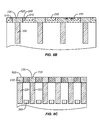
- FIGS. 2A-2C are cross-sectional views of a portion of a memory device in accordance with an embodiment.
- FIG. 2A is a cross-section taken orthogonal to bit lines 250 and includes substrate 205 having access circuitry for a plurality of memory cells.
- FIG. 2B and FIG. 2C are respective cross-sections taken orthogonal to source lines 255 .
- FIG. 2D is a top view, or plan view, of the array of memory cells illustrated in FIGS. 2A-2C .
- the second dielectric material 275 is omitted from FIG. 2D for clarity.
- Substrate 205 can be formed in a variety of ways. Any method, known or to be developed, for forming the elements of substrate 205 as described herein can be used.
- the substrate 205 includes access circuitry formed on a semiconductor substrate (not shown) for a plurality of memory cells. Access circuitry in the illustrated embodiment includes conductive word lines 265 forming the gates of access transistors, and pairs of doped regions (not shown) adjacent to the word lines 265 forming the source and drain regions of the access transistors.
- the word lines 265 extend in parallel in a first direction into and out of the cross-section illustrated in FIG. 2B .
- Substrate 205 includes an array of conductive drain contacts 220 and an array of conductive source contacts 222 .
- the conductive drain contacts 220 are electrically coupled to access transistor drain regions, and the array of conductive source contacts 222 are electrically coupled to access transistor source regions.
- access transistor source regions are shared among adjacent access transistors.
- other configurations and structures of access circuitry and contacts 220 , 222 as known or to be developed, can be used as well.
- the memory device in the illustrated embodiment includes a plurality of bit lines 250 , a plurality of first electrodes 230 , and a plurality of insulating members 240 .
- the bit lines 250 comprise conductive material extending in parallel in a second direction into and out of the cross-section illustrated in FIG. 2A .
- the insulating member 240 has a thickness 245 between a corresponding first electrode 230 and a portion of a bit line 250 acting as a second electrode.
- the first electrodes 230 are electrically coupled to corresponding conductive drain contacts 220 .
- the memory device in the illustrated embodiment includes an array of bridges 210 of memory material, the bridges 210 contacting respective first electrodes 230 and extending across the corresponding insulating member 240 to the corresponding bit line 250 .
- An inter-electrode path between the corresponding first electrode 230 and bit line 250 has a path length defined by the thickness 245 of the insulating member 240 .
- the bridges 210 in the illustrated embodiment comprise memory material having at least two solid phases that are reversible, such as chalcogenide material or other related material, by applying a current through the bridge 210 or applying a voltage across the first electrodes 230 and the bit lines 250 .
- the array of memory cells in the illustrated embodiment includes conductive elements 235 in electrical contact with corresponding source contacts 222 .
- First dielectric material 270 is between adjacent first electrodes 230 and conductive elements 235 .
- Second dielectric material 275 overlies the first electrodes 230 , bit lines 250 , and bridges 210 .
- An array of conductive vias 280 extends through the second dielectric material 275 , the conductive vias 280 in electrical contact with corresponding conductive elements 235 .
- Conductive source lines 255 extend in parallel in the first direction, the source lines 255 on the dielectric layer 275 and in electrical contact with conductive vias 280 in the plurality of conductive vias 280 .
- first electrodes 230 and bit lines 250 in the illustrated embodiment are preferably TiN or TaN.
- first electrodes 230 and bit lines 250 are TiAlN or TaAlN, or comprise, for further examples, one or more elements selected from the group consisting of Ti, W, Mo, Al, Ta, Cu, Pt, Ir, La, Ni, and Ru and alloys thereof
- FIGS. 3-10 illustrate an embodiment of a process flow for manufacturing a memory array, utilizing a memory cell as described herein.
- FIG. 3A illustrates a top view
- FIGS. 3B-3C illustrate cross-sectional views of a first step in a process flow comprising providing a substrate 205 .
- Substrate 205 includes access circuitry for a plurality of memory cells.
- Substrate 205 has a contact surface 206 with an array of conductive drain contacts 220 and an array of conductive source contacts 222 connected to the access circuitry.
- substrate 205 can be formed in a variety of ways and many other configurations and structures for access circuitry and contacts 222 , 220 can be used as well.
- a layer of conductive first electrode material 400 is formed on the contact surface 206 of the substrate 205 , resulting in the structure illustrated in FIGS. 4A-4C .
- the first electrode material 400 of the structure illustrated in FIGS. 4A-4C is patterned to form a plurality of strips 500 extending in parallel in a first direction and defining first trenches between the strips 500 .
- a first dielectric material 270 comprising, for example, silicon dioxide, is then formed in the first trenches, resulting in the structure illustrated in FIGS. 5A-5C .
- the dielectric material 270 can be formed by a fill-in process and planarized using, for example, chemical mechanical polishing CMP.
- a plurality of second trenches 600 are formed by etching the structure illustrated in FIGS. 5A-5C , resulting in the structure illustrated in FIGS. 6A-6C having a plurality of pairs of conductive elements 230 , 235 between the second trenches 600 .
- the second trenches extend in parallel in a second direction perpendicular to the first direction.
- the portions of the contact surface 206 beneath the trenches 600 are exposed.
- the pairs of conductive elements 230 , 235 include a first conductive element comprising a first electrode 230 in electrical contact with a corresponding drain contact 220 , and a second conductive element 235 in electrical contact with a corresponding source contact 222 .
- the conductive elements 230 , 235 have sidewall surfaces 610 and top surfaces 620 .
- a conformal layer of a sidewall dielectric material 700 is formed on the structure illustrated in FIGS. 6A-6C and a layer of bit line material 710 is formed on the sidewall dielectric material 700 , resulting in the structure illustrated in FIGS. 7A-7C .
- FIGS. 7A-7C is planarized to expose the top surfaces 620 of the conductive elements 230 , 235 resulting in the structure illustrated in FIGS. 8A-8C .
- a plurality of bit lines 250 comprising bit line material 710 extend in parallel in the second direction.
- the insulating members 240 in the plurality of insulating members have a thickness 245 between corresponding first electrodes 230 and bit lines 250 .
- phase change bridges 210 are patterned on the structure illustrated in FIGS. 8A-8C to form a plurality of phase change bridges 210 , resulting in the subassembly illustrated in FIGS. 9A-9C .
- the bridges 210 contact the first electrodes 230 and extend across the insulating members 240 to the bit lines 250 .
- the bridges 210 define an inter-electrode path between the corresponding first electrodes 230 and bit lines 250 defined by the thickness 245 of the insulating member 240 .
- the phase change bridges 210 may be formed, for example, by patterning a layer of dielectric material over the structure illustrated in FIGS. 8A-8C and using that layer of dielectric material as a mask for forming the phase change bridges 210 .
- a layer of second dielectric material 275 and an array of conductive vias 280 are formed on the subassembly illustrated in FIGS. 9A-9C , resulting in the structure illustrated in FIGS. 10A-10C .
- the conductive vias 280 are in electrical contact with corresponding second conductive elements 235 .
- a plurality of source lines 255 are formed on the second dielectric material 275 as illustrated in FIGS. 11A-11C , resulting in the array of memory cells as illustrated in FIGS. 2A-2D .
- the source lines 255 extend in parallel in the first direction and are in electrical contact with conductive vias 280 .
- An embodiment of a memory device as described herein includes a conductive bit line and a plurality of first electrodes.
- the memory device includes a plurality of insulating members, the insulating members having a thickness between a corresponding first electrode and a portion of the bit line acting as a second electrode.
- the memory device further includes an array of bridges of memory material having at least two solid phases, the bridges contacting respective first electrodes and extending across the corresponding insulating member to the bit line. The bridges define an inter-electrode path between the corresponding first electrode and the bit line defined by the thickness of the insulating member.
- Advantages of an embodiment described herein include memory cells having reduced cell sizes, providing an array architecture supporting high-density devices, and a method for manufacturing such structure that meets tight process variation specifications needed for large-scale memory devices.
Abstract
Description
-
- GexSbyTez
- x:y:z=2:2:5
- Or other compositions with x: 0˜5; y: 0˜5; z: 0˜10
- GeSbTe with doping, such as N—, Si—, Ti—, or other element doping may also be used.
- Formation method: By PVD sputtering or magnetron-sputtering method with reactive gases of Ar, N2, and/or He, etc chalcogenide @ the pressure of 1 mtorr˜100 mtorr. The deposition is usually done at room temperature. The collimator with aspect ratio of 1˜5 can be used to improve the fill-in performance. To improve the fill-in performance, the DC bias of several ten to several hundred volts is also used. On the other hand, the combination of DC bias and the collimator can be used simultaneously.
- The post deposition annealing treatment with vacuum or N2 ambient is sometimes needed to improve the crystallize state of chalcogenide material. The annealing temperature typically ranges 100C to 400C with an anneal time of less than 30 minutes.
- The thickness of chalcogenide material depends on the design of cell structure. In general, a chalcogenide material with thickness of higher than 8 nm can have a phase change characterization so that the material exhibits at least two stable resistance states.
2. CMR (colossal magneto resistance) material - PrxCayMnO3
- x:y=0.5:0.5
- Or other compositions with x: 0˜1; y: 0˜1
- Another CMR material that includes Mn oxide may be used
- Formation method: By PVD sputtering or magnetron-sputtering method with reactive gases of Ar, N2, O2, and/or He, etc. at the pressure of 1 mtorr˜100 mtorr. The deposition temperature can range from room temperature to ˜600C, depending on the post deposition treatment condition. A collimator with an aspect ratio of 1˜5 can be used to improve the fill-in performance. To improve the fill-in performance, the DC bias of several ten to several hundred volts is also used. On the other hand, the combination of DC bias and the collimator can be used simultaneously. A magnetic field of several ten gauss to 10,000 gauss may be applied to improve the magnetic crystallized phase.
- The post deposition annealing treatment with vacuum or N2 ambient or O2/N2 mixed ambient may be needed to improve the crystallized state of CMR material. The annealing temperature typically ranges 400C to 600C with an anneal time of less than 2 hours.
- The thickness of CMR material depends on the design of cell structure. The CMR thickness of 10 nm to 200 nm can be used to be the core material.
- A buffer layer of YBCO (YBaCuO3, a kind of high temperature superconductor material) is often used to improve the crystallized state of CMR material. The YBCO is deposited before the deposition of CMR material. The thickness of YBCO ranges 30 nm to 200 nm.
3. 2-element Compound - NixOy; TixOy; AlxOy; WxOy; ZnxOy; ZrxOy; CuxOy; etc
- x:y=0.5:0.5
- Other compositions with x: 0˜1; y: 0˜1
- Formation method:
-
- The post deposition annealing treatment with vacuum or N2 ambient or O2/N2 mixed ambient as sometimes needed to improve the oxygen distribution of metal oxide. The annealing temperature ranges 400C to 600C with an anneal time of less than 2 hours.
- 2. Reactive deposition: By PVD sputtering or magnetron-sputtering method with reactive gases of Ar/O2, Ar/N2/O2, pure O2, He/O2, He/N2/O2 etc. at the pressure of 1 mtorr˜100 mtorr, using a target of metal oxide, such as Ni, Ti, Al, W, Zn, Zr, or Cu etc. The deposition is usually done at room temperature. A collimator with an aspect ratio of 1˜5 can be used to improve the fill-in performance. To improve the fill-in performance, a DC bias of several ten to several hundred volts is also used. If desired, the combination of DC bias and the collimator can be used simultaneously.
- The post deposition annealing treatment with vacuum or N2 ambient or O2/N2 mixed ambient is sometimes needed to improve the oxygen distribution of metal oxide. The annealing temperature ranges 400C to 600C with an anneal time of less than 2 hours.
- 3. Oxidation: By a high temperature oxidation system, such as furnace or RTP system. The temperature ranges from 200C to 700C with pure O2 or N2/O2 mixed gas at a pressure of several mtorr to 1 atm. The time can range several minute to hours. Another oxidation method is plasma oxidation. An RF or a DC source plasma with pure O2 or Ar/O2 mixed gas or Ar/N2/O2 mixed gas at a pressure of 1 mtorrr to 100 mtorr is used to oxidize the surface of metal, such as Ni, Ti, Al, W, Zn, Zr, or Cu etc. The oxidation time ranges several seconds to several minutes. The oxidation temperature ranges room temperature to 300C, depending on the degree of plasma oxidation.
4. Polymer Material - TCNQ with doping of Cu, C60, Ag etc.
- PCBM-TCNQ mixed polymer
- Formation method:
- 1. Evaporation: By thermal evaporation, e-beam evaporation, or molecular beam epitaxy (MBE) system. A solid-state TCNQ and dopant pellets are co-evaporated in a single chamber. The solid-state TCNQ and dopant pellets are put in a W-boat or a Ta-boat or a ceramic boat. A high electrical current or an electron-beam is applied to melt the source so that the materials are mixed and deposited on wafers. There are no reactive chemistries or gases. The deposition is done at a pressure of 10-4 torr to 10-10 torr. The wafer temperature ranges from room temperature to 200C.
- The post deposition annealing treatment with vacuum or N2 ambient is sometimes needed to improve the composition distribution of polymer material. The annealing temperature ranges room temperature to 300C with an anneal time of less than 1 hour.
- 2. Spin-coat: By a spin-coater with the doped-TCNQ solution @ the rotation of less than 1000 rpm. After spin-coating, the wafer is put to wait the solid-state formation @ room temperature or temperature of less than 200C. The waiting time ranges from several minutes to days, depending on the temperature and on the formation conditions.
Claims (16)
Priority Applications (3)
| Application Number | Priority Date | Filing Date | Title |
|---|---|---|---|
| US11/831,819 US7884342B2 (en) | 2007-07-31 | 2007-07-31 | Phase change memory bridge cell |
| TW096132949A TWI369783B (en) | 2007-07-31 | 2007-09-04 | Memory device with phase change memory bridge cell and method of making the same |
| CN2008100031771A CN101359677B (en) | 2007-07-31 | 2008-01-15 | Phase change memory bridge |
Applications Claiming Priority (1)
| Application Number | Priority Date | Filing Date | Title |
|---|---|---|---|
| US11/831,819 US7884342B2 (en) | 2007-07-31 | 2007-07-31 | Phase change memory bridge cell |
Publications (2)
| Publication Number | Publication Date |
|---|---|
| US20090032796A1 US20090032796A1 (en) | 2009-02-05 |
| US7884342B2 true US7884342B2 (en) | 2011-02-08 |
Family
ID=40332069
Family Applications (1)
| Application Number | Title | Priority Date | Filing Date |
|---|---|---|---|
| US11/831,819 Expired - Fee Related US7884342B2 (en) | 2007-07-31 | 2007-07-31 | Phase change memory bridge cell |
Country Status (3)
| Country | Link |
|---|---|
| US (1) | US7884342B2 (en) |
| CN (1) | CN101359677B (en) |
| TW (1) | TWI369783B (en) |
Cited By (4)
| Publication number | Priority date | Publication date | Assignee | Title |
|---|---|---|---|---|
| US9741918B2 (en) | 2013-10-07 | 2017-08-22 | Hypres, Inc. | Method for increasing the integration level of superconducting electronics circuits, and a resulting circuit |
| US10566531B2 (en) | 2017-11-17 | 2020-02-18 | International Business Machines Corporation | Crosspoint fill-in memory cell with etched access device |
| US11251189B2 (en) | 2009-02-09 | 2022-02-15 | Longitude Flash Memory Solutions Ltd. | Gate fringing effect based channel formation for semiconductor device |
| US11683998B2 (en) | 2021-03-22 | 2023-06-20 | International Business Machines Corporation | Vertical phase change bridge memory cell |
Families Citing this family (5)
| Publication number | Priority date | Publication date | Assignee | Title |
|---|---|---|---|---|
| KR20090108479A (en) * | 2008-04-11 | 2009-10-15 | 삼성전자주식회사 | Method of forming a phase-change memory unit, method of manufacturing a phase-change memory device using the same, and phase-change memory device manufactured using the same |
| US8097537B2 (en) | 2010-05-25 | 2012-01-17 | Micron Technology, Inc. | Phase change memory cell structures and methods |
| JP5696378B2 (en) * | 2010-06-15 | 2015-04-08 | ソニー株式会社 | Manufacturing method of storage device |
| US8624217B2 (en) * | 2010-06-25 | 2014-01-07 | International Business Machines Corporation | Planar phase-change memory cell with parallel electrical paths |
| FR3125917B1 (en) * | 2021-07-30 | 2023-08-04 | St Microelectronics Crolles 2 Sas | Phase change memory |
Citations (163)
| Publication number | Priority date | Publication date | Assignee | Title |
|---|---|---|---|---|
| US3530441A (en) | 1969-01-15 | 1970-09-22 | Energy Conversion Devices Inc | Method and apparatus for storing and retrieving information |
| US3846767A (en) * | 1973-10-24 | 1974-11-05 | Energy Conversion Devices Inc | Method and means for resetting filament-forming memory semiconductor device |
| US4599705A (en) | 1979-12-13 | 1986-07-08 | Energy Conversion Devices, Inc. | Programmable cell for use in programmable electronic arrays |
| US4719594A (en) | 1984-11-01 | 1988-01-12 | Energy Conversion Devices, Inc. | Grooved optical data storage device including a chalcogenide memory layer |
| US4876220A (en) | 1986-05-16 | 1989-10-24 | Actel Corporation | Method of making programmable low impedance interconnect diode element |
| US4959812A (en) | 1987-12-28 | 1990-09-25 | Kabushiki Kaisha Toshiba | Electrically erasable programmable read-only memory with NAND cell structure |
| US5166096A (en) | 1991-10-29 | 1992-11-24 | International Business Machines Corporation | Process for fabricating self-aligned contact studs for semiconductor structures |
| US5166758A (en) | 1991-01-18 | 1992-11-24 | Energy Conversion Devices, Inc. | Electrically erasable phase change memory |
| US5177567A (en) | 1991-07-19 | 1993-01-05 | Energy Conversion Devices, Inc. | Thin-film structure for chalcogenide electrical switching devices and process therefor |
| US5332923A (en) | 1991-08-06 | 1994-07-26 | Nec Corporation | Semiconductor memory |
| US5391901A (en) | 1992-10-30 | 1995-02-21 | Nec Corporation | Semiconductor memory with oblique folded bit-line arrangement |
| US5515488A (en) | 1994-08-30 | 1996-05-07 | Xerox Corporation | Method and apparatus for concurrent graphical visualization of a database search and its search history |
| US5534712A (en) | 1991-01-18 | 1996-07-09 | Energy Conversion Devices, Inc. | Electrically erasable memory elements characterized by reduced current and improved thermal stability |
| US5687112A (en) | 1996-04-19 | 1997-11-11 | Energy Conversion Devices, Inc. | Multibit single cell memory element having tapered contact |
| US5789277A (en) | 1996-07-22 | 1998-08-04 | Micron Technology, Inc. | Method of making chalogenide memory device |
| US5789758A (en) | 1995-06-07 | 1998-08-04 | Micron Technology, Inc. | Chalcogenide memory cell with a plurality of chalcogenide electrodes |
| US5814527A (en) | 1996-07-22 | 1998-09-29 | Micron Technology, Inc. | Method of making small pores defined by a disposable internal spacer for use in chalcogenide memories |
| US5831276A (en) | 1995-06-07 | 1998-11-03 | Micron Technology, Inc. | Three-dimensional container diode for use with multi-state material in a non-volatile memory cell |
| US5837564A (en) | 1995-11-01 | 1998-11-17 | Micron Technology, Inc. | Method for optimal crystallization to obtain high electrical performance from chalcogenides |
| US5869843A (en) | 1995-06-07 | 1999-02-09 | Micron Technology, Inc. | Memory array having a multi-state element and method for forming such array or cells thereof |
| US5879955A (en) | 1995-06-07 | 1999-03-09 | Micron Technology, Inc. | Method for fabricating an array of ultra-small pores for chalcogenide memory cells |
| US5902704A (en) | 1997-07-02 | 1999-05-11 | Lsi Logic Corporation | Process for forming photoresist mask over integrated circuit structures with critical dimension control |
| US5952671A (en) | 1997-05-09 | 1999-09-14 | Micron Technology, Inc. | Small electrode for a chalcogenide switching device and method for fabricating same |
| US5958358A (en) | 1992-07-08 | 1999-09-28 | Yeda Research And Development Co., Ltd. | Oriented polycrystalline thin films of transition metal chalcogenides |
| US5970336A (en) | 1996-08-22 | 1999-10-19 | Micron Technology, Inc. | Method of making memory cell incorporating a chalcogenide element |
| US5985698A (en) | 1996-07-22 | 1999-11-16 | Micron Technology, Inc. | Fabrication of three dimensional container diode for use with multi-state material in a non-volatile memory cell |
| US6011725A (en) | 1997-08-01 | 2000-01-04 | Saifun Semiconductors, Ltd. | Two bit non-volatile electrically erasable and programmable semiconductor memory cell utilizing asymmetrical charge trapping |
| US6025220A (en) | 1996-06-18 | 2000-02-15 | Micron Technology, Inc. | Method of forming a polysilicon diode and devices incorporating such diode |
| US6031287A (en) | 1997-06-18 | 2000-02-29 | Micron Technology, Inc. | Contact structure and memory element incorporating the same |
| US6034882A (en) | 1998-11-16 | 2000-03-07 | Matrix Semiconductor, Inc. | Vertically stacked field programmable nonvolatile memory and method of fabrication |
| US6066870A (en) | 1996-07-16 | 2000-05-23 | Micron Technology, Inc. | Single digit line with cell contact interconnect |
| US6077674A (en) | 1999-10-27 | 2000-06-20 | Agilent Technologies Inc. | Method of producing oligonucleotide arrays with features of high purity |
| US6087674A (en) | 1996-10-28 | 2000-07-11 | Energy Conversion Devices, Inc. | Memory element with memory material comprising phase-change material and dielectric material |
| US6087269A (en) | 1998-04-20 | 2000-07-11 | Advanced Micro Devices, Inc. | Method of making an interconnect using a tungsten hard mask |
| US6114713A (en) | 1997-01-28 | 2000-09-05 | Zahorik; Russell C. | Integrated circuit memory cell having a small active area and method of forming same |
| US6117720A (en) | 1995-06-07 | 2000-09-12 | Micron Technology, Inc. | Method of making an integrated circuit electrode having a reduced contact area |
| US6147395A (en) | 1996-10-02 | 2000-11-14 | Micron Technology, Inc. | Method for fabricating a small area of contact between electrodes |
| US6177317B1 (en) | 1999-04-14 | 2001-01-23 | Macronix International Co., Ltd. | Method of making nonvolatile memory devices having reduced resistance diffusion regions |
| US6271090B1 (en) | 2000-12-22 | 2001-08-07 | Macronix International Co., Ltd. | Method for manufacturing flash memory device with dual floating gates and two bits per cell |
| US6280684B1 (en) | 1994-12-13 | 2001-08-28 | Ricoh Company, Ltd. | Sputtering target, method of producing the target, optical recording medium fabricated by using the sputtering target, and method of fabricating the optical recording medium |
| US6314014B1 (en) | 1999-12-16 | 2001-11-06 | Ovonyx, Inc. | Programmable resistance memory arrays with reference cells |
| US6320786B1 (en) | 2000-12-22 | 2001-11-20 | Macronix International Co., Ltd. | Method of controlling multi-state NROM |
| US20010055838A1 (en) | 2000-04-28 | 2001-12-27 | Matrix Semiconductor Inc. | Nonvolatile memory on SOI and compound semiconductor substrates and method of fabrication |
| US6339544B1 (en) | 2000-09-29 | 2002-01-15 | Intel Corporation | Method to enhance performance of thermal resistor device |
| US6351406B1 (en) | 1998-11-16 | 2002-02-26 | Matrix Semiconductor, Inc. | Vertically stacked field programmable nonvolatile memory and method of fabrication |
| US6372651B1 (en) | 1998-07-17 | 2002-04-16 | Advanced Micro Devices, Inc. | Method for trimming a photoresist pattern line for memory gate etching |
| US20020081833A1 (en) | 2000-12-22 | 2002-06-27 | Li Calvin K. | Patterning three dimensional structures |
| US6420216B1 (en) | 2000-03-14 | 2002-07-16 | International Business Machines Corporation | Fuse processing using dielectric planarization pillars |
| US6420215B1 (en) | 2000-04-28 | 2002-07-16 | Matrix Semiconductor, Inc. | Three-dimensional memory array and method of fabrication |
| US6429064B1 (en) | 2000-09-29 | 2002-08-06 | Intel Corporation | Reduced contact area of sidewall conductor |
| US20020168852A1 (en) * | 2001-05-11 | 2002-11-14 | Harshfield Steven T. | PCRAM memory cell and method of making same |
| US6483736B2 (en) | 1998-11-16 | 2002-11-19 | Matrix Semiconductor, Inc. | Vertically stacked field programmable nonvolatile memory and method of fabrication |
| US6487114B2 (en) | 2001-02-28 | 2002-11-26 | Macronix International Co., Ltd. | Method of reading two-bit memories of NROM cell |
| US20020182835A1 (en) | 2001-05-29 | 2002-12-05 | Quinn Robert M. | Method for manufacturing contacts for a Chalcogenide memory device |
| US6501111B1 (en) | 2000-06-30 | 2002-12-31 | Intel Corporation | Three-dimensional (3D) programmable device |
| US6511867B2 (en) | 2001-06-30 | 2003-01-28 | Ovonyx, Inc. | Utilizing atomic layer deposition for programmable device |
| US6512241B1 (en) | 2001-12-31 | 2003-01-28 | Intel Corporation | Phase change material memory device |
| US6534781B2 (en) | 2000-12-26 | 2003-03-18 | Ovonyx, Inc. | Phase-change memory bipolar array utilizing a single shallow trench isolation for creating an individual active area region for two memory array elements and one bipolar base contact |
| US6545903B1 (en) | 2001-12-17 | 2003-04-08 | Texas Instruments Incorporated | Self-aligned resistive plugs for forming memory cell with phase change material |
| US6555860B2 (en) | 2000-09-29 | 2003-04-29 | Intel Corporation | Compositionally modified resistive electrode |
| US6563156B2 (en) | 2001-03-15 | 2003-05-13 | Micron Technology, Inc. | Memory elements and methods for making same |
| US6567293B1 (en) | 2000-09-29 | 2003-05-20 | Ovonyx, Inc. | Single level metal memory cell using chalcogenide cladding |
| US6566700B2 (en) | 2001-10-11 | 2003-05-20 | Ovonyx, Inc. | Carbon-containing interfacial layer for phase-change memory |
| US6579760B1 (en) | 2002-03-28 | 2003-06-17 | Macronix International Co., Ltd. | Self-aligned, programmable phase change memory |
| US6586761B2 (en) | 2001-09-07 | 2003-07-01 | Intel Corporation | Phase change material memory device |
| US6589714B2 (en) | 2001-06-26 | 2003-07-08 | Ovonyx, Inc. | Method for making programmable resistance memory element using silylated photoresist |
| US6605527B2 (en) | 2001-06-30 | 2003-08-12 | Intel Corporation | Reduced area intersection between electrode and programming element |
| US6605821B1 (en) | 2002-05-10 | 2003-08-12 | Hewlett-Packard Development Company, L.P. | Phase change material electronic memory structure and method for forming |
| US6607974B2 (en) | 2000-07-14 | 2003-08-19 | Micron Technology, Inc. | Method of forming a contact structure in a semiconductor device |
| US6613604B2 (en) | 2001-08-02 | 2003-09-02 | Ovonyx, Inc. | Method for making small pore for use in programmable resistance memory element |
| US6617192B1 (en) | 1997-10-01 | 2003-09-09 | Ovonyx, Inc. | Electrically programmable memory element with multi-regioned contact |
| US6620715B1 (en) | 2002-03-29 | 2003-09-16 | Cypress Semiconductor Corp. | Method for forming sub-critical dimension structures in an integrated circuit |
| US6639849B2 (en) | 2002-02-28 | 2003-10-28 | Fujitsu Limited | Nonvolatile semiconductor memory device programming second dynamic reference cell according to threshold value of first dynamic reference cell |
| US6673700B2 (en) | 2001-06-30 | 2004-01-06 | Ovonyx, Inc. | Reduced area intersection between electrode and programming element |
| US20040037106A1 (en) * | 2002-08-20 | 2004-02-26 | Macronix International Co., Ltd. | Laser programmable electrically readable phase-change memory method and device |
| US20040051094A1 (en) | 2002-09-13 | 2004-03-18 | Mitsubishi Denki Kabushiki Kaisha | Non-volatile semiconductor memory device allowing shrinking of memory cell |
| US20040051161A1 (en) | 2002-04-09 | 2004-03-18 | Matsushita Electric Industrial Co., Ltd. | Non-volatile memory and the fabrication method thereof |
| US6744088B1 (en) | 2002-12-13 | 2004-06-01 | Intel Corporation | Phase change memory device on a planar composite layer |
| US6746892B2 (en) | 2002-04-04 | 2004-06-08 | Hewlett-Packard Development Company, L.P. | Low heat loss and small contact area composite electrode for a phase change media memory device |
| US20040166604A1 (en) * | 2003-02-25 | 2004-08-26 | Samsung Electronics Co. Ltd. | Phase changeable memory cells and methods of fabricating the same |
| US6791102B2 (en) | 2002-12-13 | 2004-09-14 | Intel Corporation | Phase change memory |
| US6797979B2 (en) | 2000-12-21 | 2004-09-28 | Intel Corporation | Metal structure for a phase-change memory device |
| US6800504B2 (en) | 2001-08-30 | 2004-10-05 | Micron Technology, Inc. | Integrated circuit device and fabrication using metal-doped chalcogenide materials |
| US6800563B2 (en) | 2001-10-11 | 2004-10-05 | Ovonyx, Inc. | Forming tapered lower electrode phase-change memories |
| US6805563B2 (en) | 2002-09-10 | 2004-10-19 | Enplas Corporation | Socket for electrical parts |
| US6808991B1 (en) | 2003-11-19 | 2004-10-26 | Macronix International Co., Ltd. | Method for forming twin bit cell flash memory |
| US6815704B1 (en) | 2003-09-04 | 2004-11-09 | Silicon Storage Technology, Inc. | Phase change memory device employing thermally insulating voids |
| US6830952B2 (en) | 2002-08-09 | 2004-12-14 | Macronix International Co., Ltd. | Spacer chalcogenide memory method and device |
| US20050029502A1 (en) | 2003-08-04 | 2005-02-10 | Hudgens Stephen J. | Processing phase change material to improve programming speed |
| US6859389B2 (en) | 2002-10-31 | 2005-02-22 | Dai Nippon Printing Co., Ltd. | Phase change-type memory element and process for producing the same |
| US6861267B2 (en) | 2001-09-17 | 2005-03-01 | Intel Corporation | Reducing shunts in memories with phase-change material |
| US6864500B2 (en) | 2002-04-10 | 2005-03-08 | Micron Technology, Inc. | Programmable conductor memory cell structure |
| US6867638B2 (en) | 2002-01-10 | 2005-03-15 | Silicon Storage Technology, Inc. | High voltage generation and regulation system for digital multilevel nonvolatile memory |
| US6894305B2 (en) | 2003-02-24 | 2005-05-17 | Samsung Electronics Co., Ltd. | Phase-change memory devices with a self-heater structure |
| US6903362B2 (en) | 2001-05-09 | 2005-06-07 | Science Applications International Corporation | Phase change switches and circuits coupling to electromagnetic waves containing phase change switches |
| US20050127347A1 (en) | 2003-12-12 | 2005-06-16 | Suk-Hun Choi | Methods for fabricating memory devices using sacrificial layers and memory devices fabricated by same |
| US6909107B2 (en) | 2002-12-30 | 2005-06-21 | Bae Systems, Information And Electronic Systems Integration, Inc. | Method for manufacturing sidewall contacts for a chalcogenide memory device |
| US20050167656A1 (en) | 2004-01-30 | 2005-08-04 | International Business Machines Corporation | Phase-change memory cell and method of fabricating the phase-change memory cell |
| US6927410B2 (en) | 2003-09-04 | 2005-08-09 | Silicon Storage Technology, Inc. | Memory device with discrete layers of phase change memory material |
| US6937507B2 (en) | 2003-12-05 | 2005-08-30 | Silicon Storage Technology, Inc. | Memory device and method of operating same |
| US20050191804A1 (en) | 2004-03-01 | 2005-09-01 | Taiwan Semiconductor Manufacturing Co., Ltd. | Method for forming a reduced active area in a phase change memory structure |
| US20050201182A1 (en) | 2004-03-12 | 2005-09-15 | Kenichi Osada | Semiconductor device |
| US20050212024A1 (en) | 2004-03-24 | 2005-09-29 | Infineon Technologies Ag | Memory device with an active material embedded in an insulating material |
| US20050215009A1 (en) | 2004-03-19 | 2005-09-29 | Sung-Lae Cho | Methods of forming phase-change memory devices |
| US20050211978A1 (en) * | 2004-03-24 | 2005-09-29 | Lujia Bu | Memory devices based on electric field programmable films |
| US6972430B2 (en) | 2002-02-20 | 2005-12-06 | Stmicroelectronics S.R.L. | Sublithographic contact structure, phase change memory cell with optimized heater shape, and manufacturing method thereof |
| US6992932B2 (en) | 2002-10-29 | 2006-01-31 | Saifun Semiconductors Ltd | Method circuit and system for read error detection in a non-volatile memory array |
| US20060043617A1 (en) | 2004-08-30 | 2006-03-02 | Abbott Todd R | DRAM layout with vertical FETs and method of formation |
| US7023009B2 (en) | 1997-10-01 | 2006-04-04 | Ovonyx, Inc. | Electrically programmable memory element with improved contacts |
| US7042001B2 (en) | 2004-01-29 | 2006-05-09 | Samsung Electronics Co., Ltd. | Phase change memory devices including memory elements having variable cross-sectional areas |
| US20060110878A1 (en) | 2004-11-22 | 2006-05-25 | Macronix International Co., Ltd. | Side wall active pin memory and manufacturing method |
| US20060118913A1 (en) | 2004-12-06 | 2006-06-08 | Samsung Electronics Co., Ltd. | Phase changeable memory cells and methods of forming the same |
| US7067864B2 (en) | 2001-01-30 | 2006-06-27 | Renesas Technology Corp. | SRAM having an improved capacitor |
| US7067865B2 (en) | 2003-06-06 | 2006-06-27 | Macronix International Co., Ltd. | High density chalcogenide memory cells |
| US20060154185A1 (en) | 2005-01-11 | 2006-07-13 | Taiwan Semiconductor Manufacturing Co., Ltd. | Method for forming a finely patterned resist |
| US20060175599A1 (en) | 2005-02-10 | 2006-08-10 | Infineon Technologies North America Corp. | Phase change memory cell with high read margin at low power operation |
| US20060226409A1 (en) | 2005-04-06 | 2006-10-12 | International Business Machines Corporation | Structure for confining the switching current in phase memory (PCM) cells |
| US7122281B2 (en) | 2002-02-26 | 2006-10-17 | Synopsys, Inc. | Critical dimension control using full phase and trim masks |
| US7122824B2 (en) | 2003-01-15 | 2006-10-17 | Stmicroelectronics S.R.L. | Sublithographic contact structure, in particular for a phase change memory cell, and fabrication process thereof |
| US20060234138A1 (en) | 2003-09-30 | 2006-10-19 | Rodger Fehlhaber | Hard mask arrangement |
| US7126149B2 (en) | 2004-01-21 | 2006-10-24 | Renesas Technology Corp. | Phase change memory and phase change recording medium |
| US20060286709A1 (en) | 2005-06-17 | 2006-12-21 | Macronix International Co., Ltd. | Manufacturing methods for thin film fuse phase change ram |
| US20060284214A1 (en) | 2005-06-17 | 2006-12-21 | Macronix International Co., Ltd. | Thin film fuse phase change cell with thermal isolation layer and manufacturing method |
| US20060284158A1 (en) | 2005-06-17 | 2006-12-21 | Macronix International Co., Ltd. | Self-aligned, embedded phase change ram and manufacturing method |
| US20060284279A1 (en) | 2005-06-17 | 2006-12-21 | Macronix International Co., Ltd. | Thin film fuse phase change RAM and manufacturing method |
| US20060286743A1 (en) | 2005-06-17 | 2006-12-21 | Macronix International Co., Ltd. | Method for Manufacturing a Narrow Structure on an Integrated Circuit |
| US20060284157A1 (en) | 2005-06-17 | 2006-12-21 | Macronix International Co., Ltd. | Thin film plate phase change RAM circuit and manufacturing method |
| US7166533B2 (en) | 2005-04-08 | 2007-01-23 | Infineon Technologies, Ag | Phase change memory cell defined by a pattern shrink material process |
| US20070030721A1 (en) | 2001-07-25 | 2007-02-08 | Nantero, Inc. | Device selection circuitry constructed with nanotube technology |
| US20070037101A1 (en) | 2005-08-15 | 2007-02-15 | Fujitsu Limited | Manufacture method for micro structure |
| US20070045606A1 (en) | 2005-08-30 | 2007-03-01 | Michele Magistretti | Shaping a phase change layer in a phase change memory cell |
| US20070111429A1 (en) | 2005-11-14 | 2007-05-17 | Macronix International Co., Ltd. | Method of manufacturing a pipe shaped phase change memory |
| US20070108077A1 (en) | 2005-11-16 | 2007-05-17 | Macronix International Co., Ltd. | Spacer Electrode Small Pin Phase Change Memory RAM and Manufacturing Method |
| US20070108431A1 (en) | 2005-11-15 | 2007-05-17 | Chen Shih H | I-shaped phase change memory cell |
| US20070108429A1 (en) | 2005-11-14 | 2007-05-17 | Macronix International Co., Ltd. | Pipe shaped phase change memory |
| US20070108430A1 (en) * | 2005-11-15 | 2007-05-17 | Macronix International Co., Ltd. | Thermally contained/insulated phase change memory device and method (combined) |
| US20070109843A1 (en) | 2005-11-15 | 2007-05-17 | Macronix International Co., Ltd. | Phase Change Memory Device and Manufacturing Method |
| US7220983B2 (en) | 2004-12-09 | 2007-05-22 | Macronix International Co., Ltd. | Self-aligned small contact phase-change memory method and device |
| US20070115794A1 (en) | 2005-11-21 | 2007-05-24 | Macronix International Co., Ltd. | Thermal isolation for an active-sidewall phase change memory cell |
| US20070117315A1 (en) | 2005-11-22 | 2007-05-24 | Macronix International Co., Ltd. | Memory cell device and manufacturing method |
| US20070121363A1 (en) | 2005-11-28 | 2007-05-31 | Macronix International Co., Ltd. | Phase Change Memory Cell and Manufacturing Method |
| US20070121374A1 (en) | 2005-11-15 | 2007-05-31 | Macronix International Co., Ltd. | Phase Change Memory Device and Manufacturing Method |
| US20070126040A1 (en) | 2005-11-21 | 2007-06-07 | Hsiang-Lan Lung | Vacuum cell thermal isolation for a phase change memory device |
| US20070131980A1 (en) | 2005-11-21 | 2007-06-14 | Lung Hsiang L | Vacuum jacket for phase change memory element |
| US20070131922A1 (en) | 2005-12-13 | 2007-06-14 | Macronix International Co., Ltd. | Thin Film Fuse Phase Change Cell with Thermal Isolation Pad and Manufacturing Method |
| US20070138458A1 (en) | 2005-06-17 | 2007-06-21 | Macronix International Co., Ltd. | Damascene Phase Change RAM and Manufacturing Method |
| US20070147105A1 (en) | 2005-11-28 | 2007-06-28 | Macronix International Co., Ltd. | Phase Change Memory Cell and Manufacturing Method |
| US20070155172A1 (en) | 2005-12-05 | 2007-07-05 | Macronix International Co., Ltd. | Manufacturing Method for Phase Change RAM with Electrode Layer Process |
| US20070154847A1 (en) | 2005-12-30 | 2007-07-05 | Macronix International Co., Ltd. | Chalcogenide layer etching method |
| US20070158645A1 (en) | 2006-01-11 | 2007-07-12 | Macronix International Co., Ltd. | Self-align planerized bottom electrode phase change memory and manufacturing method |
| US20070158632A1 (en) | 2006-01-09 | 2007-07-12 | Macronix International Co., Ltd. | Method for Fabricating a Pillar-Shaped Phase Change Memory Element |
| US20070158690A1 (en) | 2006-01-09 | 2007-07-12 | Macronix International Co., Ltd. | Programmable Resistive RAM and Manufacturing Method |
| US20070161186A1 (en) | 2006-01-09 | 2007-07-12 | Macronix International Co., Ltd. | Programmable Resistive RAM and Manufacturing Method |
| US20070158633A1 (en) | 2005-12-27 | 2007-07-12 | Macronix International Co., Ltd. | Method for Forming Self-Aligned Thermal Isolation Cell for a Variable Resistance Memory Array |
| US20070158862A1 (en) | 2005-11-21 | 2007-07-12 | Hsiang-Lan Lung | Vacuum jacketed electrode for phase change memory element |
| US20070173063A1 (en) | 2006-01-24 | 2007-07-26 | Macronix International Co., Ltd. | Self-aligned manufacturing method, and manufacturing method for thin film fuse phase change ram |
| US20070173019A1 (en) | 2006-01-09 | 2007-07-26 | Macronix International Co., Ltd. | Programmable Resistive Ram and Manufacturing Method |
| US20070176261A1 (en) | 2006-01-30 | 2007-08-02 | Macronix International Co., Ltd. | Vertical Side Wall Active Pin Structures in a Phase Change Memory and Manufacturing Methods |
| US7277317B2 (en) | 2003-01-31 | 2007-10-02 | Nxp B.V. | MRAM architecture for low power consumption and high selectivity |
| US20070246699A1 (en) | 2006-04-21 | 2007-10-25 | Hsiang-Lan Lung | Phase change memory cell with vacuum spacer |
| US20070257300A1 (en) | 2006-05-05 | 2007-11-08 | Macronix International Co., Ltd. | Structures and Methods of a Bistable Resistive Random Access Memory |
| US20070262388A1 (en) | 2006-05-09 | 2007-11-15 | Macronix International Co., Ltd. | Bridge Resistance Random Access Memory Device and Method With A Singular Contact Structure |
| US20070285960A1 (en) | 2006-05-24 | 2007-12-13 | Macronix International Co., Ltd. | Single-Mask Phase Change Memory Element |
-
2007
- 2007-07-31 US US11/831,819 patent/US7884342B2/en not_active Expired - Fee Related
- 2007-09-04 TW TW096132949A patent/TWI369783B/en active
-
2008
- 2008-01-15 CN CN2008100031771A patent/CN101359677B/en not_active Expired - Fee Related
Patent Citations (195)
| Publication number | Priority date | Publication date | Assignee | Title |
|---|---|---|---|---|
| US3530441A (en) | 1969-01-15 | 1970-09-22 | Energy Conversion Devices Inc | Method and apparatus for storing and retrieving information |
| US3846767A (en) * | 1973-10-24 | 1974-11-05 | Energy Conversion Devices Inc | Method and means for resetting filament-forming memory semiconductor device |
| US4599705A (en) | 1979-12-13 | 1986-07-08 | Energy Conversion Devices, Inc. | Programmable cell for use in programmable electronic arrays |
| US4719594A (en) | 1984-11-01 | 1988-01-12 | Energy Conversion Devices, Inc. | Grooved optical data storage device including a chalcogenide memory layer |
| US4876220A (en) | 1986-05-16 | 1989-10-24 | Actel Corporation | Method of making programmable low impedance interconnect diode element |
| US4959812A (en) | 1987-12-28 | 1990-09-25 | Kabushiki Kaisha Toshiba | Electrically erasable programmable read-only memory with NAND cell structure |
| US5534712A (en) | 1991-01-18 | 1996-07-09 | Energy Conversion Devices, Inc. | Electrically erasable memory elements characterized by reduced current and improved thermal stability |
| US5166758A (en) | 1991-01-18 | 1992-11-24 | Energy Conversion Devices, Inc. | Electrically erasable phase change memory |
| US5177567A (en) | 1991-07-19 | 1993-01-05 | Energy Conversion Devices, Inc. | Thin-film structure for chalcogenide electrical switching devices and process therefor |
| US5332923A (en) | 1991-08-06 | 1994-07-26 | Nec Corporation | Semiconductor memory |
| US5166096A (en) | 1991-10-29 | 1992-11-24 | International Business Machines Corporation | Process for fabricating self-aligned contact studs for semiconductor structures |
| US5958358A (en) | 1992-07-08 | 1999-09-28 | Yeda Research And Development Co., Ltd. | Oriented polycrystalline thin films of transition metal chalcogenides |
| US5391901A (en) | 1992-10-30 | 1995-02-21 | Nec Corporation | Semiconductor memory with oblique folded bit-line arrangement |
| US5515488A (en) | 1994-08-30 | 1996-05-07 | Xerox Corporation | Method and apparatus for concurrent graphical visualization of a database search and its search history |
| US6280684B1 (en) | 1994-12-13 | 2001-08-28 | Ricoh Company, Ltd. | Sputtering target, method of producing the target, optical recording medium fabricated by using the sputtering target, and method of fabricating the optical recording medium |
| US5920788A (en) | 1995-06-07 | 1999-07-06 | Micron Technology, Inc. | Chalcogenide memory cell with a plurality of chalcogenide electrodes |
| US6104038A (en) | 1995-06-07 | 2000-08-15 | Micron Technology, Inc. | Method for fabricating an array of ultra-small pores for chalcogenide memory cells |
| US5831276A (en) | 1995-06-07 | 1998-11-03 | Micron Technology, Inc. | Three-dimensional container diode for use with multi-state material in a non-volatile memory cell |
| US6117720A (en) | 1995-06-07 | 2000-09-12 | Micron Technology, Inc. | Method of making an integrated circuit electrode having a reduced contact area |
| US5869843A (en) | 1995-06-07 | 1999-02-09 | Micron Technology, Inc. | Memory array having a multi-state element and method for forming such array or cells thereof |
| US5879955A (en) | 1995-06-07 | 1999-03-09 | Micron Technology, Inc. | Method for fabricating an array of ultra-small pores for chalcogenide memory cells |
| US6077729A (en) | 1995-06-07 | 2000-06-20 | Micron Technology, Inc. | Memory array having a multi-state element and method for forming such array or cellis thereof |
| US6420725B1 (en) | 1995-06-07 | 2002-07-16 | Micron Technology, Inc. | Method and apparatus for forming an integrated circuit electrode having a reduced contact area |
| US5789758A (en) | 1995-06-07 | 1998-08-04 | Micron Technology, Inc. | Chalcogenide memory cell with a plurality of chalcogenide electrodes |
| US5837564A (en) | 1995-11-01 | 1998-11-17 | Micron Technology, Inc. | Method for optimal crystallization to obtain high electrical performance from chalcogenides |
| US5687112A (en) | 1996-04-19 | 1997-11-11 | Energy Conversion Devices, Inc. | Multibit single cell memory element having tapered contact |
| USRE37259E1 (en) | 1996-04-19 | 2001-07-03 | Energy Conversion Devices, Inc. | Multibit single cell memory element having tapered contact |
| US6025220A (en) | 1996-06-18 | 2000-02-15 | Micron Technology, Inc. | Method of forming a polysilicon diode and devices incorporating such diode |
| US6066870A (en) | 1996-07-16 | 2000-05-23 | Micron Technology, Inc. | Single digit line with cell contact interconnect |
| US5985698A (en) | 1996-07-22 | 1999-11-16 | Micron Technology, Inc. | Fabrication of three dimensional container diode for use with multi-state material in a non-volatile memory cell |
| US5814527A (en) | 1996-07-22 | 1998-09-29 | Micron Technology, Inc. | Method of making small pores defined by a disposable internal spacer for use in chalcogenide memories |
| US6111264A (en) | 1996-07-22 | 2000-08-29 | Micron Technology, Inc. | Small pores defined by a disposable internal spacer for use in chalcogenide memories |
| US5789277A (en) | 1996-07-22 | 1998-08-04 | Micron Technology, Inc. | Method of making chalogenide memory device |
| US5998244A (en) | 1996-08-22 | 1999-12-07 | Micron Technology, Inc. | Memory cell incorporating a chalcogenide element and method of making same |
| US6153890A (en) | 1996-08-22 | 2000-11-28 | Micron Technology, Inc. | Memory cell incorporating a chalcogenide element |
| US6236059B1 (en) | 1996-08-22 | 2001-05-22 | Micron Technology, Inc. | Memory cell incorporating a chalcogenide element and method of making same |
| US5970336A (en) | 1996-08-22 | 1999-10-19 | Micron Technology, Inc. | Method of making memory cell incorporating a chalcogenide element |
| US6423621B2 (en) | 1996-10-02 | 2002-07-23 | Micron Technology, Inc. | Controllable ovonic phase-change semiconductor memory device and methods of fabricating the same |
| US6147395A (en) | 1996-10-02 | 2000-11-14 | Micron Technology, Inc. | Method for fabricating a small area of contact between electrodes |
| US6150253A (en) | 1996-10-02 | 2000-11-21 | Micron Technology, Inc. | Controllable ovonic phase-change semiconductor memory device and methods of fabricating the same |
| US6287887B1 (en) | 1996-10-02 | 2001-09-11 | Micron Technology, Inc. | Method for fabricating a small area of contact between electrodes |
| US6462353B1 (en) | 1996-10-02 | 2002-10-08 | Micron Technology Inc. | Method for fabricating a small area of contact between electrodes |
| US6087674A (en) | 1996-10-28 | 2000-07-11 | Energy Conversion Devices, Inc. | Memory element with memory material comprising phase-change material and dielectric material |
| US6114713A (en) | 1997-01-28 | 2000-09-05 | Zahorik; Russell C. | Integrated circuit memory cell having a small active area and method of forming same |
| US5952671A (en) | 1997-05-09 | 1999-09-14 | Micron Technology, Inc. | Small electrode for a chalcogenide switching device and method for fabricating same |
| US6189582B1 (en) | 1997-05-09 | 2001-02-20 | Micron Technology, Inc. | Small electrode for a chalcogenide switching device and method for fabricating same |
| US6031287A (en) | 1997-06-18 | 2000-02-29 | Micron Technology, Inc. | Contact structure and memory element incorporating the same |
| US5902704A (en) | 1997-07-02 | 1999-05-11 | Lsi Logic Corporation | Process for forming photoresist mask over integrated circuit structures with critical dimension control |
| US6011725A (en) | 1997-08-01 | 2000-01-04 | Saifun Semiconductors, Ltd. | Two bit non-volatile electrically erasable and programmable semiconductor memory cell utilizing asymmetrical charge trapping |
| US6617192B1 (en) | 1997-10-01 | 2003-09-09 | Ovonyx, Inc. | Electrically programmable memory element with multi-regioned contact |
| US7023009B2 (en) | 1997-10-01 | 2006-04-04 | Ovonyx, Inc. | Electrically programmable memory element with improved contacts |
| US6087269A (en) | 1998-04-20 | 2000-07-11 | Advanced Micro Devices, Inc. | Method of making an interconnect using a tungsten hard mask |
| US6372651B1 (en) | 1998-07-17 | 2002-04-16 | Advanced Micro Devices, Inc. | Method for trimming a photoresist pattern line for memory gate etching |
| US6034882A (en) | 1998-11-16 | 2000-03-07 | Matrix Semiconductor, Inc. | Vertically stacked field programmable nonvolatile memory and method of fabrication |
| US6185122B1 (en) | 1998-11-16 | 2001-02-06 | Matrix Semiconductor, Inc. | Vertically stacked field programmable nonvolatile memory and method of fabrication |
| US6483736B2 (en) | 1998-11-16 | 2002-11-19 | Matrix Semiconductor, Inc. | Vertically stacked field programmable nonvolatile memory and method of fabrication |
| US6351406B1 (en) | 1998-11-16 | 2002-02-26 | Matrix Semiconductor, Inc. | Vertically stacked field programmable nonvolatile memory and method of fabrication |
| US6177317B1 (en) | 1999-04-14 | 2001-01-23 | Macronix International Co., Ltd. | Method of making nonvolatile memory devices having reduced resistance diffusion regions |
| US6077674A (en) | 1999-10-27 | 2000-06-20 | Agilent Technologies Inc. | Method of producing oligonucleotide arrays with features of high purity |
| US6314014B1 (en) | 1999-12-16 | 2001-11-06 | Ovonyx, Inc. | Programmable resistance memory arrays with reference cells |
| US6420216B1 (en) | 2000-03-14 | 2002-07-16 | International Business Machines Corporation | Fuse processing using dielectric planarization pillars |
| US6888750B2 (en) | 2000-04-28 | 2005-05-03 | Matrix Semiconductor, Inc. | Nonvolatile memory on SOI and compound semiconductor substrates and method of fabrication |
| US20010055838A1 (en) | 2000-04-28 | 2001-12-27 | Matrix Semiconductor Inc. | Nonvolatile memory on SOI and compound semiconductor substrates and method of fabrication |
| US6420215B1 (en) | 2000-04-28 | 2002-07-16 | Matrix Semiconductor, Inc. | Three-dimensional memory array and method of fabrication |
| US6501111B1 (en) | 2000-06-30 | 2002-12-31 | Intel Corporation | Three-dimensional (3D) programmable device |
| US6607974B2 (en) | 2000-07-14 | 2003-08-19 | Micron Technology, Inc. | Method of forming a contact structure in a semiconductor device |
| US6339544B1 (en) | 2000-09-29 | 2002-01-15 | Intel Corporation | Method to enhance performance of thermal resistor device |
| US6621095B2 (en) | 2000-09-29 | 2003-09-16 | Ovonyx, Inc. | Method to enhance performance of thermal resistor device |
| US6597009B2 (en) | 2000-09-29 | 2003-07-22 | Intel Corporation | Reduced contact area of sidewall conductor |
| US6429064B1 (en) | 2000-09-29 | 2002-08-06 | Intel Corporation | Reduced contact area of sidewall conductor |
| US6567293B1 (en) | 2000-09-29 | 2003-05-20 | Ovonyx, Inc. | Single level metal memory cell using chalcogenide cladding |
| US6555860B2 (en) | 2000-09-29 | 2003-04-29 | Intel Corporation | Compositionally modified resistive electrode |
| US6797979B2 (en) | 2000-12-21 | 2004-09-28 | Intel Corporation | Metal structure for a phase-change memory device |
| US6271090B1 (en) | 2000-12-22 | 2001-08-07 | Macronix International Co., Ltd. | Method for manufacturing flash memory device with dual floating gates and two bits per cell |
| US6627530B2 (en) | 2000-12-22 | 2003-09-30 | Matrix Semiconductor, Inc. | Patterning three dimensional structures |
| US6320786B1 (en) | 2000-12-22 | 2001-11-20 | Macronix International Co., Ltd. | Method of controlling multi-state NROM |
| US20020081833A1 (en) | 2000-12-22 | 2002-06-27 | Li Calvin K. | Patterning three dimensional structures |
| US6534781B2 (en) | 2000-12-26 | 2003-03-18 | Ovonyx, Inc. | Phase-change memory bipolar array utilizing a single shallow trench isolation for creating an individual active area region for two memory array elements and one bipolar base contact |
| US6593176B2 (en) | 2000-12-26 | 2003-07-15 | Ovonyx, Inc. | Method for forming phase-change memory bipolar array utilizing a single shallow trench isolation for creating an individual active area region for two memory array elements and one bipolar base contact |
| US7067864B2 (en) | 2001-01-30 | 2006-06-27 | Renesas Technology Corp. | SRAM having an improved capacitor |
| US6487114B2 (en) | 2001-02-28 | 2002-11-26 | Macronix International Co., Ltd. | Method of reading two-bit memories of NROM cell |
| US6563156B2 (en) | 2001-03-15 | 2003-05-13 | Micron Technology, Inc. | Memory elements and methods for making same |
| US6903362B2 (en) | 2001-05-09 | 2005-06-07 | Science Applications International Corporation | Phase change switches and circuits coupling to electromagnetic waves containing phase change switches |
| US20020168852A1 (en) * | 2001-05-11 | 2002-11-14 | Harshfield Steven T. | PCRAM memory cell and method of making same |
| US6514788B2 (en) | 2001-05-29 | 2003-02-04 | Bae Systems Information And Electronic Systems Integration Inc. | Method for manufacturing contacts for a Chalcogenide memory device |
| US20020182835A1 (en) | 2001-05-29 | 2002-12-05 | Quinn Robert M. | Method for manufacturing contacts for a Chalcogenide memory device |
| US6589714B2 (en) | 2001-06-26 | 2003-07-08 | Ovonyx, Inc. | Method for making programmable resistance memory element using silylated photoresist |
| US6605527B2 (en) | 2001-06-30 | 2003-08-12 | Intel Corporation | Reduced area intersection between electrode and programming element |
| US6673700B2 (en) | 2001-06-30 | 2004-01-06 | Ovonyx, Inc. | Reduced area intersection between electrode and programming element |
| US6511867B2 (en) | 2001-06-30 | 2003-01-28 | Ovonyx, Inc. | Utilizing atomic layer deposition for programmable device |
| US20070030721A1 (en) | 2001-07-25 | 2007-02-08 | Nantero, Inc. | Device selection circuitry constructed with nanotube technology |
| US6613604B2 (en) | 2001-08-02 | 2003-09-02 | Ovonyx, Inc. | Method for making small pore for use in programmable resistance memory element |
| US6800504B2 (en) | 2001-08-30 | 2004-10-05 | Micron Technology, Inc. | Integrated circuit device and fabrication using metal-doped chalcogenide materials |
| US6586761B2 (en) | 2001-09-07 | 2003-07-01 | Intel Corporation | Phase change material memory device |
| US6861267B2 (en) | 2001-09-17 | 2005-03-01 | Intel Corporation | Reducing shunts in memories with phase-change material |
| US6566700B2 (en) | 2001-10-11 | 2003-05-20 | Ovonyx, Inc. | Carbon-containing interfacial layer for phase-change memory |
| US6800563B2 (en) | 2001-10-11 | 2004-10-05 | Ovonyx, Inc. | Forming tapered lower electrode phase-change memories |
| US6933516B2 (en) | 2001-10-11 | 2005-08-23 | Ovonyx, Inc. | Forming tapered lower electrode phase-change memories |
| US6545903B1 (en) | 2001-12-17 | 2003-04-08 | Texas Instruments Incorporated | Self-aligned resistive plugs for forming memory cell with phase change material |
| US6512241B1 (en) | 2001-12-31 | 2003-01-28 | Intel Corporation | Phase change material memory device |
| US6867638B2 (en) | 2002-01-10 | 2005-03-15 | Silicon Storage Technology, Inc. | High voltage generation and regulation system for digital multilevel nonvolatile memory |
| US6972430B2 (en) | 2002-02-20 | 2005-12-06 | Stmicroelectronics S.R.L. | Sublithographic contact structure, phase change memory cell with optimized heater shape, and manufacturing method thereof |
| US7122281B2 (en) | 2002-02-26 | 2006-10-17 | Synopsys, Inc. | Critical dimension control using full phase and trim masks |
| US6639849B2 (en) | 2002-02-28 | 2003-10-28 | Fujitsu Limited | Nonvolatile semiconductor memory device programming second dynamic reference cell according to threshold value of first dynamic reference cell |
| US6579760B1 (en) | 2002-03-28 | 2003-06-17 | Macronix International Co., Ltd. | Self-aligned, programmable phase change memory |
| US6620715B1 (en) | 2002-03-29 | 2003-09-16 | Cypress Semiconductor Corp. | Method for forming sub-critical dimension structures in an integrated circuit |
| US6746892B2 (en) | 2002-04-04 | 2004-06-08 | Hewlett-Packard Development Company, L.P. | Low heat loss and small contact area composite electrode for a phase change media memory device |
| US20040051161A1 (en) | 2002-04-09 | 2004-03-18 | Matsushita Electric Industrial Co., Ltd. | Non-volatile memory and the fabrication method thereof |
| US6864500B2 (en) | 2002-04-10 | 2005-03-08 | Micron Technology, Inc. | Programmable conductor memory cell structure |
| US7132675B2 (en) | 2002-04-10 | 2006-11-07 | Micron Technology, Inc. | Programmable conductor memory cell structure and method therefor |
| US6605821B1 (en) | 2002-05-10 | 2003-08-12 | Hewlett-Packard Development Company, L.P. | Phase change material electronic memory structure and method for forming |
| US20050093022A1 (en) | 2002-08-09 | 2005-05-05 | Macronix International Co., Ltd. | Spacer chalcogenide memory device |
| US6864503B2 (en) | 2002-08-09 | 2005-03-08 | Macronix International Co., Ltd. | Spacer chalcogenide memory method and device |
| US6830952B2 (en) | 2002-08-09 | 2004-12-14 | Macronix International Co., Ltd. | Spacer chalcogenide memory method and device |
| US7033856B2 (en) | 2002-08-09 | 2006-04-25 | Macronix International Co. Ltd | Spacer chalcogenide memory method |
| US6850432B2 (en) | 2002-08-20 | 2005-02-01 | Macronix International Co., Ltd. | Laser programmable electrically readable phase-change memory method and device |
| US20040037106A1 (en) * | 2002-08-20 | 2004-02-26 | Macronix International Co., Ltd. | Laser programmable electrically readable phase-change memory method and device |
| US6805563B2 (en) | 2002-09-10 | 2004-10-19 | Enplas Corporation | Socket for electrical parts |
| US20040051094A1 (en) | 2002-09-13 | 2004-03-18 | Mitsubishi Denki Kabushiki Kaisha | Non-volatile semiconductor memory device allowing shrinking of memory cell |
| US6992932B2 (en) | 2002-10-29 | 2006-01-31 | Saifun Semiconductors Ltd | Method circuit and system for read error detection in a non-volatile memory array |
| US6859389B2 (en) | 2002-10-31 | 2005-02-22 | Dai Nippon Printing Co., Ltd. | Phase change-type memory element and process for producing the same |
| US6791102B2 (en) | 2002-12-13 | 2004-09-14 | Intel Corporation | Phase change memory |
| US6744088B1 (en) | 2002-12-13 | 2004-06-01 | Intel Corporation | Phase change memory device on a planar composite layer |
| US6909107B2 (en) | 2002-12-30 | 2005-06-21 | Bae Systems, Information And Electronic Systems Integration, Inc. | Method for manufacturing sidewall contacts for a chalcogenide memory device |
| US7122824B2 (en) | 2003-01-15 | 2006-10-17 | Stmicroelectronics S.R.L. | Sublithographic contact structure, in particular for a phase change memory cell, and fabrication process thereof |
| US7277317B2 (en) | 2003-01-31 | 2007-10-02 | Nxp B.V. | MRAM architecture for low power consumption and high selectivity |
| US6894305B2 (en) | 2003-02-24 | 2005-05-17 | Samsung Electronics Co., Ltd. | Phase-change memory devices with a self-heater structure |
| US20040166604A1 (en) * | 2003-02-25 | 2004-08-26 | Samsung Electronics Co. Ltd. | Phase changeable memory cells and methods of fabricating the same |
| US7067865B2 (en) | 2003-06-06 | 2006-06-27 | Macronix International Co., Ltd. | High density chalcogenide memory cells |
| US20050029502A1 (en) | 2003-08-04 | 2005-02-10 | Hudgens Stephen J. | Processing phase change material to improve programming speed |
| US6815704B1 (en) | 2003-09-04 | 2004-11-09 | Silicon Storage Technology, Inc. | Phase change memory device employing thermally insulating voids |
| US6927410B2 (en) | 2003-09-04 | 2005-08-09 | Silicon Storage Technology, Inc. | Memory device with discrete layers of phase change memory material |
| US20060234138A1 (en) | 2003-09-30 | 2006-10-19 | Rodger Fehlhaber | Hard mask arrangement |
| US6808991B1 (en) | 2003-11-19 | 2004-10-26 | Macronix International Co., Ltd. | Method for forming twin bit cell flash memory |
| US6937507B2 (en) | 2003-12-05 | 2005-08-30 | Silicon Storage Technology, Inc. | Memory device and method of operating same |
| US20050127347A1 (en) | 2003-12-12 | 2005-06-16 | Suk-Hun Choi | Methods for fabricating memory devices using sacrificial layers and memory devices fabricated by same |
| US7126149B2 (en) | 2004-01-21 | 2006-10-24 | Renesas Technology Corp. | Phase change memory and phase change recording medium |
| US7042001B2 (en) | 2004-01-29 | 2006-05-09 | Samsung Electronics Co., Ltd. | Phase change memory devices including memory elements having variable cross-sectional areas |
| US6936840B2 (en) | 2004-01-30 | 2005-08-30 | International Business Machines Corporation | Phase-change memory cell and method of fabricating the phase-change memory cell |
| US20050167656A1 (en) | 2004-01-30 | 2005-08-04 | International Business Machines Corporation | Phase-change memory cell and method of fabricating the phase-change memory cell |
| US20050191804A1 (en) | 2004-03-01 | 2005-09-01 | Taiwan Semiconductor Manufacturing Co., Ltd. | Method for forming a reduced active area in a phase change memory structure |
| US20050201182A1 (en) | 2004-03-12 | 2005-09-15 | Kenichi Osada | Semiconductor device |
| US20050215009A1 (en) | 2004-03-19 | 2005-09-29 | Sung-Lae Cho | Methods of forming phase-change memory devices |
| US20050211978A1 (en) * | 2004-03-24 | 2005-09-29 | Lujia Bu | Memory devices based on electric field programmable films |
| US20050212024A1 (en) | 2004-03-24 | 2005-09-29 | Infineon Technologies Ag | Memory device with an active material embedded in an insulating material |
| US20060043617A1 (en) | 2004-08-30 | 2006-03-02 | Abbott Todd R | DRAM layout with vertical FETs and method of formation |
| US20060108667A1 (en) | 2004-11-22 | 2006-05-25 | Macronix International Co., Ltd. | Method for manufacturing a small pin on integrated circuits or other devices |
| US20060110878A1 (en) | 2004-11-22 | 2006-05-25 | Macronix International Co., Ltd. | Side wall active pin memory and manufacturing method |
| US20060118913A1 (en) | 2004-12-06 | 2006-06-08 | Samsung Electronics Co., Ltd. | Phase changeable memory cells and methods of forming the same |
| US7220983B2 (en) | 2004-12-09 | 2007-05-22 | Macronix International Co., Ltd. | Self-aligned small contact phase-change memory method and device |
| US20060154185A1 (en) | 2005-01-11 | 2006-07-13 | Taiwan Semiconductor Manufacturing Co., Ltd. | Method for forming a finely patterned resist |
| US20060175599A1 (en) | 2005-02-10 | 2006-08-10 | Infineon Technologies North America Corp. | Phase change memory cell with high read margin at low power operation |
| US7214958B2 (en) | 2005-02-10 | 2007-05-08 | Infineon Technologies Ag | Phase change memory cell with high read margin at low power operation |
| US20060226409A1 (en) | 2005-04-06 | 2006-10-12 | International Business Machines Corporation | Structure for confining the switching current in phase memory (PCM) cells |
| US7166533B2 (en) | 2005-04-08 | 2007-01-23 | Infineon Technologies, Ag | Phase change memory cell defined by a pattern shrink material process |
| US20060284214A1 (en) | 2005-06-17 | 2006-12-21 | Macronix International Co., Ltd. | Thin film fuse phase change cell with thermal isolation layer and manufacturing method |
| US20060286743A1 (en) | 2005-06-17 | 2006-12-21 | Macronix International Co., Ltd. | Method for Manufacturing a Narrow Structure on an Integrated Circuit |
| US20060284279A1 (en) | 2005-06-17 | 2006-12-21 | Macronix International Co., Ltd. | Thin film fuse phase change RAM and manufacturing method |
| US20060284158A1 (en) | 2005-06-17 | 2006-12-21 | Macronix International Co., Ltd. | Self-aligned, embedded phase change ram and manufacturing method |
| US20060284157A1 (en) | 2005-06-17 | 2006-12-21 | Macronix International Co., Ltd. | Thin film plate phase change RAM circuit and manufacturing method |
| US20070138458A1 (en) | 2005-06-17 | 2007-06-21 | Macronix International Co., Ltd. | Damascene Phase Change RAM and Manufacturing Method |
| US20070224726A1 (en) | 2005-06-17 | 2007-09-27 | Macronix International Co., Ltd. | Thin film plate phase change ram circuit and manufacturing method |
| US20060286709A1 (en) | 2005-06-17 | 2006-12-21 | Macronix International Co., Ltd. | Manufacturing methods for thin film fuse phase change ram |
| US20070037101A1 (en) | 2005-08-15 | 2007-02-15 | Fujitsu Limited | Manufacture method for micro structure |
| US20070045606A1 (en) | 2005-08-30 | 2007-03-01 | Michele Magistretti | Shaping a phase change layer in a phase change memory cell |
| US20070111429A1 (en) | 2005-11-14 | 2007-05-17 | Macronix International Co., Ltd. | Method of manufacturing a pipe shaped phase change memory |
| US20070108429A1 (en) | 2005-11-14 | 2007-05-17 | Macronix International Co., Ltd. | Pipe shaped phase change memory |
| US20070108431A1 (en) | 2005-11-15 | 2007-05-17 | Chen Shih H | I-shaped phase change memory cell |
| US20070109836A1 (en) | 2005-11-15 | 2007-05-17 | Macronix International Co., Ltd. | Thermally insulated phase change memory device and manufacturing method |
| US20070109843A1 (en) | 2005-11-15 | 2007-05-17 | Macronix International Co., Ltd. | Phase Change Memory Device and Manufacturing Method |
| US20070108430A1 (en) * | 2005-11-15 | 2007-05-17 | Macronix International Co., Ltd. | Thermally contained/insulated phase change memory device and method (combined) |
| US20070121374A1 (en) | 2005-11-15 | 2007-05-31 | Macronix International Co., Ltd. | Phase Change Memory Device and Manufacturing Method |
| US20070108077A1 (en) | 2005-11-16 | 2007-05-17 | Macronix International Co., Ltd. | Spacer Electrode Small Pin Phase Change Memory RAM and Manufacturing Method |
| US20070158862A1 (en) | 2005-11-21 | 2007-07-12 | Hsiang-Lan Lung | Vacuum jacketed electrode for phase change memory element |
| US20070131980A1 (en) | 2005-11-21 | 2007-06-14 | Lung Hsiang L | Vacuum jacket for phase change memory element |
| US20070126040A1 (en) | 2005-11-21 | 2007-06-07 | Hsiang-Lan Lung | Vacuum cell thermal isolation for a phase change memory device |
| US20070115794A1 (en) | 2005-11-21 | 2007-05-24 | Macronix International Co., Ltd. | Thermal isolation for an active-sidewall phase change memory cell |
| US20070117315A1 (en) | 2005-11-22 | 2007-05-24 | Macronix International Co., Ltd. | Memory cell device and manufacturing method |
| US20070147105A1 (en) | 2005-11-28 | 2007-06-28 | Macronix International Co., Ltd. | Phase Change Memory Cell and Manufacturing Method |
| US20070121363A1 (en) | 2005-11-28 | 2007-05-31 | Macronix International Co., Ltd. | Phase Change Memory Cell and Manufacturing Method |
| US20070155172A1 (en) | 2005-12-05 | 2007-07-05 | Macronix International Co., Ltd. | Manufacturing Method for Phase Change RAM with Electrode Layer Process |
| US20070131922A1 (en) | 2005-12-13 | 2007-06-14 | Macronix International Co., Ltd. | Thin Film Fuse Phase Change Cell with Thermal Isolation Pad and Manufacturing Method |
| US20070158633A1 (en) | 2005-12-27 | 2007-07-12 | Macronix International Co., Ltd. | Method for Forming Self-Aligned Thermal Isolation Cell for a Variable Resistance Memory Array |
| US20070154847A1 (en) | 2005-12-30 | 2007-07-05 | Macronix International Co., Ltd. | Chalcogenide layer etching method |
| US20070161186A1 (en) | 2006-01-09 | 2007-07-12 | Macronix International Co., Ltd. | Programmable Resistive RAM and Manufacturing Method |
| US20070158690A1 (en) | 2006-01-09 | 2007-07-12 | Macronix International Co., Ltd. | Programmable Resistive RAM and Manufacturing Method |
| US20070158632A1 (en) | 2006-01-09 | 2007-07-12 | Macronix International Co., Ltd. | Method for Fabricating a Pillar-Shaped Phase Change Memory Element |
| US20070173019A1 (en) | 2006-01-09 | 2007-07-26 | Macronix International Co., Ltd. | Programmable Resistive Ram and Manufacturing Method |
| US20070158645A1 (en) | 2006-01-11 | 2007-07-12 | Macronix International Co., Ltd. | Self-align planerized bottom electrode phase change memory and manufacturing method |
| US20070173063A1 (en) | 2006-01-24 | 2007-07-26 | Macronix International Co., Ltd. | Self-aligned manufacturing method, and manufacturing method for thin film fuse phase change ram |
| US20070176261A1 (en) | 2006-01-30 | 2007-08-02 | Macronix International Co., Ltd. | Vertical Side Wall Active Pin Structures in a Phase Change Memory and Manufacturing Methods |
| US20070246699A1 (en) | 2006-04-21 | 2007-10-25 | Hsiang-Lan Lung | Phase change memory cell with vacuum spacer |
| US20070257300A1 (en) | 2006-05-05 | 2007-11-08 | Macronix International Co., Ltd. | Structures and Methods of a Bistable Resistive Random Access Memory |
| US20070262388A1 (en) | 2006-05-09 | 2007-11-15 | Macronix International Co., Ltd. | Bridge Resistance Random Access Memory Device and Method With A Singular Contact Structure |
| US20070285960A1 (en) | 2006-05-24 | 2007-12-13 | Macronix International Co., Ltd. | Single-Mask Phase Change Memory Element |
Non-Patent Citations (53)
| Title |
|---|
| "Magnetic Bit Boost," www.sciencenews.org , Dec. 18 & 25, 2004, p. 389, vol. 166. |
| "Magnetic Bit Boost," www.sciencenews.org <http://www.sciencenews.org>, Dec. 18 & 25, 2004, p. 389, vol. 166. |
| "New Memories Tap Spin, Gird for Battle," Science News, Apr. 3, 1999, p. 223, vol. 155. |
| "Optimized Thermal Capacitance in a Phase Change Memory Cell Design," IPCOM000141986D, IP.com Prior Art Database, Oct. 18, 2006, 4 pp. |
| "Remembering on the Cheap," www.sciencenews.org , Mar. 19, 2005, p. 189, vol. 167. |
| "Remembering on the Cheap," www.sciencenews.org <http://www.sciencenews.org>, Mar. 19, 2005, p. 189, vol. 167. |
| "Thermal Conductivity of Crystalline Dielectrics" in CRC Handbook of Chemistry and Physics, Internet Version 2007, (87th edition), David R. Lide, ed. Taylor and Francis, Boca Raton, FL. |
| Adler, D. et al., "Threshold Switching in Chalgenid-Glass Thin Films," J. Appl/Phys 51(6), Jun. 1980, pp. 3289-3309. |
| Adler, David, "Amorphous-Semiconductor Devices," Sci. Amer., vol. 236, pp. 36-48, May 1977. |
| Ahn, S. J. et al., "Highly Reliable 5nm Contact Cell Technology for 256Mb PRAM," VLSI Technology, Digest of Technical Papers, Jun. 14-16, 2005, pp. 98-99. |
| Ahn, S.J. et al., "A Highly Manufacturable High Density Phase Change Memory og 64 Mb and Beyond," IEEE IEDM 2004, pp. 907-910. |
| Axon Technologies Corporation paper: Technology Description, pp. 1-6. |
| Bedeschi, F. et al., "4-MB MOSFET-Selected Phase-Change Memory Experimental Chip," IEEE, 2004, 4 pp. |
| Blake thesis, "Investigation of GeTeSb5 Chalcogenide Films for Use as an Analog Memory,"AFIT/GE/ENG/00M-04, Mar. 2000 121 pages. |
| Chao, D-S. et al., "Low Programming Current Phase Change Memory Cell with Double gst Thermally Confined Structure," VLSI-TSA 2007, International symposium Apr. 23-25, 2007, 2pp. |
| Chen, et al., "Non-Volatile Resistive Switching for Advanced Memory Applications," IEEE IEDM, Dec. 5-7, 2005, 4 pp. |
| Cho, S.L. et al., "Highly Scalable On-axis Confined Cell Structure for High Density PRAM beyond 256Mb," 2005 Symposium on VLSI Technology Digest of Technical Papers, pp. 96-97. |
| Gibson, G.A. et al., "Phase-change Recording Medium that Enables Ultrahigh-density Electron-beam Data Storage," Applied Physics Letter, 2005, 3 pp., vol. 86. |
| Gill, Manzur et al., "A High-Performance Nonvolatile Memory Technology for Stand-Alone Memory and Embedded Applications," 2002 IEEE-ISSCC Technical Digest (TD 12.4), 7 pp. |
| Ha, Y.H. et al., "An Edge Contact Type Cell from Phase Change RAM Featuring Very Low Power Consumtion," 2003 Symposium on VSLI Technology Digest of Technical Papers, pp. 175-176. |
| Happ, T.D. et al., "Novel None-Mask Self-Heating Pillar Phase Change Memory," 2006 Symposium on VLSI Technology, 2 pp. |
| Haring Bolivar, P. et al., "Lateral Design for Phase Change Random Access Memory Cells with Low-Current Consumption," presented at 3rd E*PCOS 04 Symposium in Balzers, Principality of Liechtenstein, Sep. 4-7, 2004, 4 pp. |
| Horii, H. et al., "A Novel Cell Technology Using N-doped GeSbTe Films for Phase Change RAM," 2003 Symposium on VLSI Technology Digest of Technical Papers, pp. 177-178. |
| Hudgens, S. et al., "Overview of Phase-Change Chalcogenide Nonvolatile Memory Technology," MRS Bulletin, Nov. 2004, pp. 829-832. |
| Hwang, Y. N. et al., "Full Integration and Reliability Evaluation of Phase-Change RAM Based on 0.24 mum-CMOS Technologies," 2003 Symposium on VLSI Technology Digest of Technical Papers, pp. 173-174. |
| Hwang, Y. N. et al., "Full Integration and Reliability Evaluation of Phase-Change RAM Based on 0.24 μm-CMOS Technologies," 2003 Symposium on VLSI Technology Digest of Technical Papers, pp. 173-174. |
| Iwasaki, Hiroko et al, "Completely Erasable Phase Change Optical Disk," Jpn. J. Appl. Phys., Feb. 1992, pp. 461-465, vol. 31. |
| Jeong, C.W. et al., "Switching Current Scaling and Reliability Evaluation in PRAM," IEEE Non-Volatile Semiconductor Memory Workshop, Monterey, CA, 2004, pp. 28-29 and workshop cover sheet. |
| Kim, Kinam et al., "Reliability Investigations for Manufacturable High Density PRAM," IEEE 43rd Annual International Reliability Physics Symposium, San Jose, 2005, pp. 157-162. |
| Kojima, Rie et al., "Ge-Sn-Sb-Te Phase-change Recording Material Having High Crystallization Speed," Proceedings of PCOS 2000, pp. 36-41. |
| Lacita, A. L.; "Electrothermal and Phase-change Dynamics in Chalcogenide-based Memories," IEEE IEDM 2004, 4 pp. |
| Lai, Stefan, "Current Status of the Phase Change Memory and Its Future," IEEE IEDM 2003, pp. 255-258. |
| Lai, Stephan et al., OUM-A 180 nm Nonvolatile Memory Cell Element Technology for Stand Alone and Embedded Applications, IEEE IEDM 2001, pp. 803-806. |
| Lankhorst, Martijn H. R., et al; Low-Cost and Nanoscale Non-Volatile Memory Concept for Future Silicon Chips, Mar. 13, 2005, 6 pp., Nature Materials Advance Online Publication, www.nature.com/naturematerials. |
| Mott, Nevill, "Electrons in Glass," Nobel Lecture, Dec. 8, 1977, Physics, 1977, pp. 403-413. |
| Ovonyx Non-Confidential paper entitled "Ovonic Unified Memory," Dec. 1999, pp. 1-80. |
| Ovshinsky, Sandford R., "Reversible Electrical Switching Phenomena in Disordered Structures," Physical Review Letters, vol. 21, No. 20, Nov. 11, 1968, pp. 1450-1453. |
| Owen, Alan E. et al., "Electronic Conduction and Switching in Chalcogenide Glasses," IEEE Transactions on Electron Devices, vol. Ed. 20, No. 2, Feb. 1973, pp. 105-122. |
| Pellizer, F. et al., "Novel muTrench Phase-Change Memory Cell for Embedded and Stand-Alone Non-Volatile Memory Applications," 2004 Symposium on VLSI Technology Digest of Technical Papers, pp. 18-19. |
| Pellizer, F. et al., "Novel μTrench Phase-Change Memory Cell for Embedded and Stand-Alone Non-Volatile Memory Applications," 2004 Symposium on VLSI Technology Digest of Technical Papers, pp. 18-19. |
| Pirovano, Agostino et al., "Reliability Study of Phase-Change Nonvolatile Memories," IEEE Transactions on Device and Materials Reliability, Sep. 2004, pp. 422-427, vol. 4, No. 3. |
| Prakash, S. et al., "A Guideline for Designing Chalcogenide-Based Glasses for Threshold Switching Characteristics," IEEE Electron Device Letters, vol. 18, No. 2, Feb. 1997, pp. 45-47. |
| Radaelli, A. et al., "Electronic Switching Effect and Phase-Change Transition in Chalcogenide Materials," IEEE Electron Device Letters, Oct. 2004, pp. 684-686, vol. 25, No. 10. |
| Rochefort, C. et al., "Manufacturing of High Aspect-Ration p-n Junctions Using Vapor Phase Doping for Application in Multi-Resurf Devices," IEEE 2002. |
| Schafft, Harry A. et al., "Thermal Conductivity Measurements of Thin Films Silicon Dioxide", Proceedings of the IEEE 1989 International Conference on Microelectronic Test Structures, vol. 2, No. 1, Mar. 1989, pp. 121-124. |
| Strauss, Karl F. et al., "Overview of Radiation Tolerant Unlimited Write Cycle Non-Volatile Memory," IEEE 2000. |
| Subramanian, Vivek et al., "Low Leakage Germanium-Seeded Laterally-Crystallized Single-Grain 100-nm TFT's for Vertical lntergration Applications," IEEE Electron Device Letters, vol. 20, No. 7, Jul. 1999. |
| Wicker, Guy et al., Nonvolatile, High Density, High Performance Phase Change Memory, 1999, :http://klabs.org/richcontent/MAPLDCon99/Papers/P21-Tyson-P.PDF#search=nonvolatile%20 high%20density%20high%20performance%20phase%20change%20memory <http://klabs.org/richcontent/MAPLDCon99/Papers/P21-Tyson-P.PDF#search='nonvolatile%20high%20density%20high%20performance%20phase%20change%20memory>', 8 pages. |
| Wicker, Guy, "A Comprehensive Model of Submicron Chalcogenide Switching Devices," Doctoral Dissertation, Wayne State University, Detroit, MI, 1996. |
| Wolf, Stanley, Excerpt from: Silicon Processing for the VLSI Era-vol. 4, pp. 674-679, 2004. |
| Wuttig, Matthias, "Towards a Universal Memory?" Nature Materials, Apr. 2005, pp. 265-266, vol. 4. |
| Yi, J. H. et al., "Novel Cell Structure of PRAM with Thin Metal Layer Inserted GeSbTe," IEEE IEDM 2003, 4 pages. |
| Yonehara, T. et al., "Control of Grain Boundary Location by Selective Nucleation Over Amorphous Substrates," Mat. Res. Soc. Symp. Proc., vol. 106, 1998, pp. 21-26. |
Cited By (7)
| Publication number | Priority date | Publication date | Assignee | Title |
|---|---|---|---|---|
| US11251189B2 (en) | 2009-02-09 | 2022-02-15 | Longitude Flash Memory Solutions Ltd. | Gate fringing effect based channel formation for semiconductor device |
| US11950412B2 (en) | 2009-02-09 | 2024-04-02 | Longitude Flash Memory Solutions Ltd. | Gate fringing effect based channel formation for semiconductor device |
| US9741918B2 (en) | 2013-10-07 | 2017-08-22 | Hypres, Inc. | Method for increasing the integration level of superconducting electronics circuits, and a resulting circuit |
| US10283694B2 (en) | 2013-10-07 | 2019-05-07 | Hypres, Inc. | Method for increasing the integration level of superconducting electronics circuits, and a resulting circuit |
| US10566531B2 (en) | 2017-11-17 | 2020-02-18 | International Business Machines Corporation | Crosspoint fill-in memory cell with etched access device |
| US10622562B2 (en) | 2017-11-17 | 2020-04-14 | International Business Machines Corporation | Crosspoint fill-in memory cell with etched access device |
| US11683998B2 (en) | 2021-03-22 | 2023-06-20 | International Business Machines Corporation | Vertical phase change bridge memory cell |
Also Published As
| Publication number | Publication date |
|---|---|
| CN101359677B (en) | 2011-08-31 |
| TWI369783B (en) | 2012-08-01 |
| TW200913251A (en) | 2009-03-16 |
| US20090032796A1 (en) | 2009-02-05 |
| CN101359677A (en) | 2009-02-04 |
Similar Documents
| Publication | Publication Date | Title |
|---|---|---|
| US7696506B2 (en) | Memory cell with memory material insulation and manufacturing method | |
| US7569844B2 (en) | Memory cell sidewall contacting side electrode | |
| US7514367B2 (en) | Method for manufacturing a narrow structure on an integrated circuit | |
| US8106376B2 (en) | Method for manufacturing a resistor random access memory with a self-aligned air gap insulator | |
| US7463512B2 (en) | Memory element with reduced-current phase change element | |
| US8513637B2 (en) | 4F2 self align fin bottom electrodes FET drive phase change memory | |
| US7642539B2 (en) | Thin film fuse phase change cell with thermal isolation pad and manufacturing method | |
| US7755076B2 (en) | 4F2 self align side wall active phase change memory | |
| US7599217B2 (en) | Memory cell device and manufacturing method | |
| US7397060B2 (en) | Pipe shaped phase change memory | |
| US7863655B2 (en) | Phase change memory cells with dual access devices | |
| US7919766B2 (en) | Method for making self aligning pillar memory cell device | |
| US7682868B2 (en) | Method for making a keyhole opening during the manufacture of a memory cell | |
| US7785920B2 (en) | Method for making a pillar-type phase change memory element | |
| US7473576B2 (en) | Method for making a self-converged void and bottom electrode for memory cell | |
| US7879645B2 (en) | Fill-in etching free pore device | |
| US7884342B2 (en) | Phase change memory bridge cell | |
| US7510929B2 (en) | Method for making memory cell device | |
| US7527985B2 (en) | Method for manufacturing a resistor random access memory with reduced active area and reduced contact areas | |
| US7956344B2 (en) | Memory cell with memory element contacting ring-shaped upper end of bottom electrode | |
| US7972893B2 (en) | Memory device manufacturing method | |
| US8610098B2 (en) | Phase change memory bridge cell with diode isolation device |
Legal Events
| Date | Code | Title | Description |
|---|---|---|---|
| AS | Assignment |
Owner name: MACRONIX INTERNATIONAL CO., LTD., TAIWAN Free format text: ASSIGNMENT OF ASSIGNORS INTEREST;ASSIGNOR:LUNG, HSIANG-LAN;REEL/FRAME:019627/0223 Effective date: 20070713 |
|
| STCF | Information on status: patent grant |
Free format text: PATENTED CASE |
|
| FPAY | Fee payment |
Year of fee payment: 4 |
|
| MAFP | Maintenance fee payment |
Free format text: PAYMENT OF MAINTENANCE FEE, 8TH YEAR, LARGE ENTITY (ORIGINAL EVENT CODE: M1552) Year of fee payment: 8 |
|
| FEPP | Fee payment procedure |
Free format text: MAINTENANCE FEE REMINDER MAILED (ORIGINAL EVENT CODE: REM.); ENTITY STATUS OF PATENT OWNER: LARGE ENTITY |
|
| LAPS | Lapse for failure to pay maintenance fees |
Free format text: PATENT EXPIRED FOR FAILURE TO PAY MAINTENANCE FEES (ORIGINAL EVENT CODE: EXP.); ENTITY STATUS OF PATENT OWNER: LARGE ENTITY |
|
| STCH | Information on status: patent discontinuation |
Free format text: PATENT EXPIRED DUE TO NONPAYMENT OF MAINTENANCE FEES UNDER 37 CFR 1.362 |
|
| FP | Lapsed due to failure to pay maintenance fee |
Effective date: 20230208 |