US7906858B2 - Contact securing element for bonding a contact wire and for establishing an electrical connection - Google Patents
Contact securing element for bonding a contact wire and for establishing an electrical connection Download PDFInfo
- Publication number
- US7906858B2 US7906858B2 US11/436,794 US43679406A US7906858B2 US 7906858 B2 US7906858 B2 US 7906858B2 US 43679406 A US43679406 A US 43679406A US 7906858 B2 US7906858 B2 US 7906858B2
- Authority
- US
- United States
- Prior art keywords
- contact
- wire
- securing element
- additional
- contact point
- Prior art date
- Legal status (The legal status is an assumption and is not a legal conclusion. Google has not performed a legal analysis and makes no representation as to the accuracy of the status listed.)
- Expired - Lifetime, expires
Links
Images


Classifications
-
- H—ELECTRICITY
- H01—ELECTRIC ELEMENTS
- H01L—SEMICONDUCTOR DEVICES NOT COVERED BY CLASS H10
- H01L24/00—Arrangements for connecting or disconnecting semiconductor or solid-state bodies; Methods or apparatus related thereto
- H01L24/80—Methods for connecting semiconductor or other solid state bodies using means for bonding being attached to, or being formed on, the surface to be connected
- H01L24/85—Methods for connecting semiconductor or other solid state bodies using means for bonding being attached to, or being formed on, the surface to be connected using a wire connector
-
- B—PERFORMING OPERATIONS; TRANSPORTING
- B23—MACHINE TOOLS; METAL-WORKING NOT OTHERWISE PROVIDED FOR
- B23K—SOLDERING OR UNSOLDERING; WELDING; CLADDING OR PLATING BY SOLDERING OR WELDING; CUTTING BY APPLYING HEAT LOCALLY, e.g. FLAME CUTTING; WORKING BY LASER BEAM
- B23K20/00—Non-electric welding by applying impact or other pressure, with or without the application of heat, e.g. cladding or plating
- B23K20/002—Non-electric welding by applying impact or other pressure, with or without the application of heat, e.g. cladding or plating specially adapted for particular articles or work
- B23K20/004—Wire welding
-
- H—ELECTRICITY
- H01—ELECTRIC ELEMENTS
- H01L—SEMICONDUCTOR DEVICES NOT COVERED BY CLASS H10
- H01L24/00—Arrangements for connecting or disconnecting semiconductor or solid-state bodies; Methods or apparatus related thereto
- H01L24/01—Means for bonding being attached to, or being formed on, the surface to be connected, e.g. chip-to-package, die-attach, "first-level" interconnects; Manufacturing methods related thereto
- H01L24/42—Wire connectors; Manufacturing methods related thereto
- H01L24/47—Structure, shape, material or disposition of the wire connectors after the connecting process
- H01L24/48—Structure, shape, material or disposition of the wire connectors after the connecting process of an individual wire connector
-
- H—ELECTRICITY
- H01—ELECTRIC ELEMENTS
- H01R—ELECTRICALLY-CONDUCTIVE CONNECTIONS; STRUCTURAL ASSOCIATIONS OF A PLURALITY OF MUTUALLY-INSULATED ELECTRICAL CONNECTING ELEMENTS; COUPLING DEVICES; CURRENT COLLECTORS
- H01R43/00—Apparatus or processes specially adapted for manufacturing, assembling, maintaining, or repairing of line connectors or current collectors or for joining electric conductors
- H01R43/02—Apparatus or processes specially adapted for manufacturing, assembling, maintaining, or repairing of line connectors or current collectors or for joining electric conductors for soldered or welded connections
- H01R43/0207—Ultrasonic-, H.F.-, cold- or impact welding
-
- B—PERFORMING OPERATIONS; TRANSPORTING
- B23—MACHINE TOOLS; METAL-WORKING NOT OTHERWISE PROVIDED FOR
- B23K—SOLDERING OR UNSOLDERING; WELDING; CLADDING OR PLATING BY SOLDERING OR WELDING; CUTTING BY APPLYING HEAT LOCALLY, e.g. FLAME CUTTING; WORKING BY LASER BEAM
- B23K2101/00—Articles made by soldering, welding or cutting
- B23K2101/36—Electric or electronic devices
-
- H—ELECTRICITY
- H01—ELECTRIC ELEMENTS
- H01L—SEMICONDUCTOR DEVICES NOT COVERED BY CLASS H10
- H01L2224/00—Indexing scheme for arrangements for connecting or disconnecting semiconductor or solid-state bodies and methods related thereto as covered by H01L24/00
- H01L2224/01—Means for bonding being attached to, or being formed on, the surface to be connected, e.g. chip-to-package, die-attach, "first-level" interconnects; Manufacturing methods related thereto
- H01L2224/42—Wire connectors; Manufacturing methods related thereto
- H01L2224/44—Structure, shape, material or disposition of the wire connectors prior to the connecting process
- H01L2224/45—Structure, shape, material or disposition of the wire connectors prior to the connecting process of an individual wire connector
- H01L2224/45001—Core members of the connector
- H01L2224/45099—Material
- H01L2224/451—Material with a principal constituent of the material being a metal or a metalloid, e.g. boron (B), silicon (Si), germanium (Ge), arsenic (As), antimony (Sb), tellurium (Te) and polonium (Po), and alloys thereof
- H01L2224/45117—Material with a principal constituent of the material being a metal or a metalloid, e.g. boron (B), silicon (Si), germanium (Ge), arsenic (As), antimony (Sb), tellurium (Te) and polonium (Po), and alloys thereof the principal constituent melting at a temperature of greater than or equal to 400°C and less than 950°C
- H01L2224/45124—Aluminium (Al) as principal constituent
-
- H—ELECTRICITY
- H01—ELECTRIC ELEMENTS
- H01L—SEMICONDUCTOR DEVICES NOT COVERED BY CLASS H10
- H01L2224/00—Indexing scheme for arrangements for connecting or disconnecting semiconductor or solid-state bodies and methods related thereto as covered by H01L24/00
- H01L2224/01—Means for bonding being attached to, or being formed on, the surface to be connected, e.g. chip-to-package, die-attach, "first-level" interconnects; Manufacturing methods related thereto
- H01L2224/42—Wire connectors; Manufacturing methods related thereto
- H01L2224/44—Structure, shape, material or disposition of the wire connectors prior to the connecting process
- H01L2224/45—Structure, shape, material or disposition of the wire connectors prior to the connecting process of an individual wire connector
- H01L2224/45001—Core members of the connector
- H01L2224/45099—Material
- H01L2224/451—Material with a principal constituent of the material being a metal or a metalloid, e.g. boron (B), silicon (Si), germanium (Ge), arsenic (As), antimony (Sb), tellurium (Te) and polonium (Po), and alloys thereof
- H01L2224/45138—Material with a principal constituent of the material being a metal or a metalloid, e.g. boron (B), silicon (Si), germanium (Ge), arsenic (As), antimony (Sb), tellurium (Te) and polonium (Po), and alloys thereof the principal constituent melting at a temperature of greater than or equal to 950°C and less than 1550°C
- H01L2224/45144—Gold (Au) as principal constituent
-
- H—ELECTRICITY
- H01—ELECTRIC ELEMENTS
- H01L—SEMICONDUCTOR DEVICES NOT COVERED BY CLASS H10
- H01L2224/00—Indexing scheme for arrangements for connecting or disconnecting semiconductor or solid-state bodies and methods related thereto as covered by H01L24/00
- H01L2224/01—Means for bonding being attached to, or being formed on, the surface to be connected, e.g. chip-to-package, die-attach, "first-level" interconnects; Manufacturing methods related thereto
- H01L2224/42—Wire connectors; Manufacturing methods related thereto
- H01L2224/47—Structure, shape, material or disposition of the wire connectors after the connecting process
- H01L2224/48—Structure, shape, material or disposition of the wire connectors after the connecting process of an individual wire connector
- H01L2224/4805—Shape
- H01L2224/4809—Loop shape
- H01L2224/48091—Arched
-
- H—ELECTRICITY
- H01—ELECTRIC ELEMENTS
- H01L—SEMICONDUCTOR DEVICES NOT COVERED BY CLASS H10
- H01L2224/00—Indexing scheme for arrangements for connecting or disconnecting semiconductor or solid-state bodies and methods related thereto as covered by H01L24/00
- H01L2224/01—Means for bonding being attached to, or being formed on, the surface to be connected, e.g. chip-to-package, die-attach, "first-level" interconnects; Manufacturing methods related thereto
- H01L2224/42—Wire connectors; Manufacturing methods related thereto
- H01L2224/47—Structure, shape, material or disposition of the wire connectors after the connecting process
- H01L2224/48—Structure, shape, material or disposition of the wire connectors after the connecting process of an individual wire connector
- H01L2224/481—Disposition
- H01L2224/48151—Connecting between a semiconductor or solid-state body and an item not being a semiconductor or solid-state body, e.g. chip-to-substrate, chip-to-passive
- H01L2224/48221—Connecting between a semiconductor or solid-state body and an item not being a semiconductor or solid-state body, e.g. chip-to-substrate, chip-to-passive the body and the item being stacked
- H01L2224/48245—Connecting between a semiconductor or solid-state body and an item not being a semiconductor or solid-state body, e.g. chip-to-substrate, chip-to-passive the body and the item being stacked the item being metallic
- H01L2224/48247—Connecting between a semiconductor or solid-state body and an item not being a semiconductor or solid-state body, e.g. chip-to-substrate, chip-to-passive the body and the item being stacked the item being metallic connecting the wire to a bond pad of the item
-
- H—ELECTRICITY
- H01—ELECTRIC ELEMENTS
- H01L—SEMICONDUCTOR DEVICES NOT COVERED BY CLASS H10
- H01L2224/00—Indexing scheme for arrangements for connecting or disconnecting semiconductor or solid-state bodies and methods related thereto as covered by H01L24/00
- H01L2224/01—Means for bonding being attached to, or being formed on, the surface to be connected, e.g. chip-to-package, die-attach, "first-level" interconnects; Manufacturing methods related thereto
- H01L2224/42—Wire connectors; Manufacturing methods related thereto
- H01L2224/47—Structure, shape, material or disposition of the wire connectors after the connecting process
- H01L2224/48—Structure, shape, material or disposition of the wire connectors after the connecting process of an individual wire connector
- H01L2224/484—Connecting portions
- H01L2224/48455—Details of wedge bonds
-
- H—ELECTRICITY
- H01—ELECTRIC ELEMENTS
- H01L—SEMICONDUCTOR DEVICES NOT COVERED BY CLASS H10
- H01L2224/00—Indexing scheme for arrangements for connecting or disconnecting semiconductor or solid-state bodies and methods related thereto as covered by H01L24/00
- H01L2224/01—Means for bonding being attached to, or being formed on, the surface to be connected, e.g. chip-to-package, die-attach, "first-level" interconnects; Manufacturing methods related thereto
- H01L2224/42—Wire connectors; Manufacturing methods related thereto
- H01L2224/47—Structure, shape, material or disposition of the wire connectors after the connecting process
- H01L2224/48—Structure, shape, material or disposition of the wire connectors after the connecting process of an individual wire connector
- H01L2224/484—Connecting portions
- H01L2224/48463—Connecting portions the connecting portion on the bonding area of the semiconductor or solid-state body being a ball bond
- H01L2224/48465—Connecting portions the connecting portion on the bonding area of the semiconductor or solid-state body being a ball bond the other connecting portion not on the bonding area being a wedge bond, i.e. ball-to-wedge, regular stitch
-
- H—ELECTRICITY
- H01—ELECTRIC ELEMENTS
- H01L—SEMICONDUCTOR DEVICES NOT COVERED BY CLASS H10
- H01L2224/00—Indexing scheme for arrangements for connecting or disconnecting semiconductor or solid-state bodies and methods related thereto as covered by H01L24/00
- H01L2224/01—Means for bonding being attached to, or being formed on, the surface to be connected, e.g. chip-to-package, die-attach, "first-level" interconnects; Manufacturing methods related thereto
- H01L2224/42—Wire connectors; Manufacturing methods related thereto
- H01L2224/47—Structure, shape, material or disposition of the wire connectors after the connecting process
- H01L2224/48—Structure, shape, material or disposition of the wire connectors after the connecting process of an individual wire connector
- H01L2224/485—Material
- H01L2224/48505—Material at the bonding interface
- H01L2224/48599—Principal constituent of the connecting portion of the wire connector being Gold (Au)
-
- H—ELECTRICITY
- H01—ELECTRIC ELEMENTS
- H01L—SEMICONDUCTOR DEVICES NOT COVERED BY CLASS H10
- H01L2224/00—Indexing scheme for arrangements for connecting or disconnecting semiconductor or solid-state bodies and methods related thereto as covered by H01L24/00
- H01L2224/01—Means for bonding being attached to, or being formed on, the surface to be connected, e.g. chip-to-package, die-attach, "first-level" interconnects; Manufacturing methods related thereto
- H01L2224/42—Wire connectors; Manufacturing methods related thereto
- H01L2224/47—Structure, shape, material or disposition of the wire connectors after the connecting process
- H01L2224/48—Structure, shape, material or disposition of the wire connectors after the connecting process of an individual wire connector
- H01L2224/485—Material
- H01L2224/48505—Material at the bonding interface
- H01L2224/48699—Principal constituent of the connecting portion of the wire connector being Aluminium (Al)
-
- H—ELECTRICITY
- H01—ELECTRIC ELEMENTS
- H01L—SEMICONDUCTOR DEVICES NOT COVERED BY CLASS H10
- H01L2224/00—Indexing scheme for arrangements for connecting or disconnecting semiconductor or solid-state bodies and methods related thereto as covered by H01L24/00
- H01L2224/01—Means for bonding being attached to, or being formed on, the surface to be connected, e.g. chip-to-package, die-attach, "first-level" interconnects; Manufacturing methods related thereto
- H01L2224/42—Wire connectors; Manufacturing methods related thereto
- H01L2224/47—Structure, shape, material or disposition of the wire connectors after the connecting process
- H01L2224/48—Structure, shape, material or disposition of the wire connectors after the connecting process of an individual wire connector
- H01L2224/4899—Auxiliary members for wire connectors, e.g. flow-barriers, reinforcing structures, spacers, alignment aids
- H01L2224/48996—Auxiliary members for wire connectors, e.g. flow-barriers, reinforcing structures, spacers, alignment aids being formed on an item to be connected not being a semiconductor or solid-state body
- H01L2224/48997—Reinforcing structures
-
- H—ELECTRICITY
- H01—ELECTRIC ELEMENTS
- H01L—SEMICONDUCTOR DEVICES NOT COVERED BY CLASS H10
- H01L2224/00—Indexing scheme for arrangements for connecting or disconnecting semiconductor or solid-state bodies and methods related thereto as covered by H01L24/00
- H01L2224/74—Apparatus for manufacturing arrangements for connecting or disconnecting semiconductor or solid-state bodies and for methods related thereto
- H01L2224/78—Apparatus for connecting with wire connectors
- H01L2224/7825—Means for applying energy, e.g. heating means
- H01L2224/783—Means for applying energy, e.g. heating means by means of pressure
- H01L2224/78301—Capillary
-
- H—ELECTRICITY
- H01—ELECTRIC ELEMENTS
- H01L—SEMICONDUCTOR DEVICES NOT COVERED BY CLASS H10
- H01L2224/00—Indexing scheme for arrangements for connecting or disconnecting semiconductor or solid-state bodies and methods related thereto as covered by H01L24/00
- H01L2224/80—Methods for connecting semiconductor or other solid state bodies using means for bonding being attached to, or being formed on, the surface to be connected
- H01L2224/85—Methods for connecting semiconductor or other solid state bodies using means for bonding being attached to, or being formed on, the surface to be connected using a wire connector
- H01L2224/8512—Aligning
- H01L2224/85148—Aligning involving movement of a part of the bonding apparatus
- H01L2224/85169—Aligning involving movement of a part of the bonding apparatus being the upper part of the bonding apparatus, i.e. bonding head, e.g. capillary or wedge
- H01L2224/8518—Translational movements
- H01L2224/85181—Translational movements connecting first on the semiconductor or solid-state body, i.e. on-chip, regular stitch
-
- H—ELECTRICITY
- H01—ELECTRIC ELEMENTS
- H01L—SEMICONDUCTOR DEVICES NOT COVERED BY CLASS H10
- H01L2224/00—Indexing scheme for arrangements for connecting or disconnecting semiconductor or solid-state bodies and methods related thereto as covered by H01L24/00
- H01L2224/80—Methods for connecting semiconductor or other solid state bodies using means for bonding being attached to, or being formed on, the surface to be connected
- H01L2224/85—Methods for connecting semiconductor or other solid state bodies using means for bonding being attached to, or being formed on, the surface to be connected using a wire connector
- H01L2224/852—Applying energy for connecting
- H01L2224/85201—Compression bonding
- H01L2224/85205—Ultrasonic bonding
-
- H—ELECTRICITY
- H01—ELECTRIC ELEMENTS
- H01L—SEMICONDUCTOR DEVICES NOT COVERED BY CLASS H10
- H01L2224/00—Indexing scheme for arrangements for connecting or disconnecting semiconductor or solid-state bodies and methods related thereto as covered by H01L24/00
- H01L2224/80—Methods for connecting semiconductor or other solid state bodies using means for bonding being attached to, or being formed on, the surface to be connected
- H01L2224/85—Methods for connecting semiconductor or other solid state bodies using means for bonding being attached to, or being formed on, the surface to be connected using a wire connector
- H01L2224/85909—Post-treatment of the connector or wire bonding area
- H01L2224/85951—Forming additional members, e.g. for reinforcing
-
- H—ELECTRICITY
- H01—ELECTRIC ELEMENTS
- H01L—SEMICONDUCTOR DEVICES NOT COVERED BY CLASS H10
- H01L2224/00—Indexing scheme for arrangements for connecting or disconnecting semiconductor or solid-state bodies and methods related thereto as covered by H01L24/00
- H01L2224/80—Methods for connecting semiconductor or other solid state bodies using means for bonding being attached to, or being formed on, the surface to be connected
- H01L2224/85—Methods for connecting semiconductor or other solid state bodies using means for bonding being attached to, or being formed on, the surface to be connected using a wire connector
- H01L2224/85986—Specific sequence of steps, e.g. repetition of manufacturing steps, time sequence
-
- H—ELECTRICITY
- H01—ELECTRIC ELEMENTS
- H01L—SEMICONDUCTOR DEVICES NOT COVERED BY CLASS H10
- H01L24/00—Arrangements for connecting or disconnecting semiconductor or solid-state bodies; Methods or apparatus related thereto
- H01L24/01—Means for bonding being attached to, or being formed on, the surface to be connected, e.g. chip-to-package, die-attach, "first-level" interconnects; Manufacturing methods related thereto
- H01L24/42—Wire connectors; Manufacturing methods related thereto
- H01L24/44—Structure, shape, material or disposition of the wire connectors prior to the connecting process
- H01L24/45—Structure, shape, material or disposition of the wire connectors prior to the connecting process of an individual wire connector
-
- H—ELECTRICITY
- H01—ELECTRIC ELEMENTS
- H01L—SEMICONDUCTOR DEVICES NOT COVERED BY CLASS H10
- H01L24/00—Arrangements for connecting or disconnecting semiconductor or solid-state bodies; Methods or apparatus related thereto
- H01L24/74—Apparatus for manufacturing arrangements for connecting or disconnecting semiconductor or solid-state bodies
- H01L24/78—Apparatus for connecting with wire connectors
-
- H—ELECTRICITY
- H01—ELECTRIC ELEMENTS
- H01L—SEMICONDUCTOR DEVICES NOT COVERED BY CLASS H10
- H01L2924/00—Indexing scheme for arrangements or methods for connecting or disconnecting semiconductor or solid-state bodies as covered by H01L24/00
- H01L2924/0001—Technical content checked by a classifier
- H01L2924/00014—Technical content checked by a classifier the subject-matter covered by the group, the symbol of which is combined with the symbol of this group, being disclosed without further technical details
-
- H—ELECTRICITY
- H01—ELECTRIC ELEMENTS
- H01L—SEMICONDUCTOR DEVICES NOT COVERED BY CLASS H10
- H01L2924/00—Indexing scheme for arrangements or methods for connecting or disconnecting semiconductor or solid-state bodies as covered by H01L24/00
- H01L2924/01—Chemical elements
- H01L2924/01005—Boron [B]
-
- H—ELECTRICITY
- H01—ELECTRIC ELEMENTS
- H01L—SEMICONDUCTOR DEVICES NOT COVERED BY CLASS H10
- H01L2924/00—Indexing scheme for arrangements or methods for connecting or disconnecting semiconductor or solid-state bodies as covered by H01L24/00
- H01L2924/01—Chemical elements
- H01L2924/01006—Carbon [C]
-
- H—ELECTRICITY
- H01—ELECTRIC ELEMENTS
- H01L—SEMICONDUCTOR DEVICES NOT COVERED BY CLASS H10
- H01L2924/00—Indexing scheme for arrangements or methods for connecting or disconnecting semiconductor or solid-state bodies as covered by H01L24/00
- H01L2924/01—Chemical elements
- H01L2924/01013—Aluminum [Al]
-
- H—ELECTRICITY
- H01—ELECTRIC ELEMENTS
- H01L—SEMICONDUCTOR DEVICES NOT COVERED BY CLASS H10
- H01L2924/00—Indexing scheme for arrangements or methods for connecting or disconnecting semiconductor or solid-state bodies as covered by H01L24/00
- H01L2924/01—Chemical elements
- H01L2924/01032—Germanium [Ge]
-
- H—ELECTRICITY
- H01—ELECTRIC ELEMENTS
- H01L—SEMICONDUCTOR DEVICES NOT COVERED BY CLASS H10
- H01L2924/00—Indexing scheme for arrangements or methods for connecting or disconnecting semiconductor or solid-state bodies as covered by H01L24/00
- H01L2924/01—Chemical elements
- H01L2924/01039—Yttrium [Y]
-
- H—ELECTRICITY
- H01—ELECTRIC ELEMENTS
- H01L—SEMICONDUCTOR DEVICES NOT COVERED BY CLASS H10
- H01L2924/00—Indexing scheme for arrangements or methods for connecting or disconnecting semiconductor or solid-state bodies as covered by H01L24/00
- H01L2924/01—Chemical elements
- H01L2924/01057—Lanthanum [La]
-
- H—ELECTRICITY
- H01—ELECTRIC ELEMENTS
- H01L—SEMICONDUCTOR DEVICES NOT COVERED BY CLASS H10
- H01L2924/00—Indexing scheme for arrangements or methods for connecting or disconnecting semiconductor or solid-state bodies as covered by H01L24/00
- H01L2924/01—Chemical elements
- H01L2924/01079—Gold [Au]
-
- Y—GENERAL TAGGING OF NEW TECHNOLOGICAL DEVELOPMENTS; GENERAL TAGGING OF CROSS-SECTIONAL TECHNOLOGIES SPANNING OVER SEVERAL SECTIONS OF THE IPC; TECHNICAL SUBJECTS COVERED BY FORMER USPC CROSS-REFERENCE ART COLLECTIONS [XRACs] AND DIGESTS
- Y10—TECHNICAL SUBJECTS COVERED BY FORMER USPC
- Y10T—TECHNICAL SUBJECTS COVERED BY FORMER US CLASSIFICATION
- Y10T29/00—Metal working
- Y10T29/49—Method of mechanical manufacture
- Y10T29/49002—Electrical device making
- Y10T29/49117—Conductor or circuit manufacturing
- Y10T29/49124—On flat or curved insulated base, e.g., printed circuit, etc.
- Y10T29/4913—Assembling to base an electrical component, e.g., capacitor, etc.
- Y10T29/49144—Assembling to base an electrical component, e.g., capacitor, etc. by metal fusion
-
- Y—GENERAL TAGGING OF NEW TECHNOLOGICAL DEVELOPMENTS; GENERAL TAGGING OF CROSS-SECTIONAL TECHNOLOGIES SPANNING OVER SEVERAL SECTIONS OF THE IPC; TECHNICAL SUBJECTS COVERED BY FORMER USPC CROSS-REFERENCE ART COLLECTIONS [XRACs] AND DIGESTS
- Y10—TECHNICAL SUBJECTS COVERED BY FORMER USPC
- Y10T—TECHNICAL SUBJECTS COVERED BY FORMER US CLASSIFICATION
- Y10T29/00—Metal working
- Y10T29/49—Method of mechanical manufacture
- Y10T29/49002—Electrical device making
- Y10T29/49117—Conductor or circuit manufacturing
- Y10T29/49124—On flat or curved insulated base, e.g., printed circuit, etc.
- Y10T29/49147—Assembling terminal to base
- Y10T29/49149—Assembling terminal to base by metal fusion bonding
-
- Y—GENERAL TAGGING OF NEW TECHNOLOGICAL DEVELOPMENTS; GENERAL TAGGING OF CROSS-SECTIONAL TECHNOLOGIES SPANNING OVER SEVERAL SECTIONS OF THE IPC; TECHNICAL SUBJECTS COVERED BY FORMER USPC CROSS-REFERENCE ART COLLECTIONS [XRACs] AND DIGESTS
- Y10—TECHNICAL SUBJECTS COVERED BY FORMER USPC
- Y10T—TECHNICAL SUBJECTS COVERED BY FORMER US CLASSIFICATION
- Y10T29/00—Metal working
- Y10T29/49—Method of mechanical manufacture
- Y10T29/49002—Electrical device making
- Y10T29/49117—Conductor or circuit manufacturing
- Y10T29/49174—Assembling terminal to elongated conductor
- Y10T29/49179—Assembling terminal to elongated conductor by metal fusion bonding
-
- Y—GENERAL TAGGING OF NEW TECHNOLOGICAL DEVELOPMENTS; GENERAL TAGGING OF CROSS-SECTIONAL TECHNOLOGIES SPANNING OVER SEVERAL SECTIONS OF THE IPC; TECHNICAL SUBJECTS COVERED BY FORMER USPC CROSS-REFERENCE ART COLLECTIONS [XRACs] AND DIGESTS
- Y10—TECHNICAL SUBJECTS COVERED BY FORMER USPC
- Y10T—TECHNICAL SUBJECTS COVERED BY FORMER US CLASSIFICATION
- Y10T29/00—Metal working
- Y10T29/53—Means to assemble or disassemble
- Y10T29/5313—Means to assemble electrical device
- Y10T29/532—Conductor
Definitions
- the present invention relates to a method for establishing an electrical connection, features and a contact point.
- a single-wire contacting method called bonding, is known for establishing an electrical connection between at least two contact surfaces.
- individual wires in particular, gold or aluminum wires
- bonding the contact wire is bonded to the contact surfaces by applying ultrasonic pressure and heat.
- the free end of the bonding wire is first melted to form a ball, by applying thermal energy, and subsequently pressed onto the first contact surface, using a bonding capillary.
- the contact wire bonds to the contact surface as a result of atomic bonding forces (material fusion) arising at the boundary between the contact surface and the contact wire.
- the ball that was previously melted on is deformed into a nail head.
- the contact wire is then led to the second contact surface, using the wire-bonding tool.
- the contact wire is formed into a loop.
- the contact wire is then pressed onto the second contact surface with the wire-bonding tool by again applying ultrasonic pressure and heat. This produces necking of the contact wire, causing the latter to form a rupture joint at which the contact wire breaks away from the second contact surface as the wire-bonding tool moves on.
- the contact wire is bonded to the second contact surface by a “stitch,” with atomic bonding forces again arising at the boundary between the contact wire and the second contact surface.
- This known ball-wedge bonding method (ball bonding with the first contact surface, and stitch bonding with the second contact surface) produces a strong dependency between the materials of the contact wire and the contact surface, thus forming strong atomic bonding forces at the boundaries. Particularly when contacting the second contact surface, a relatively weak surface bonding forms between the stitch and the contact surface, resulting in contacting errors, particularly in the case of contact surfaces made of hard-to-bond materials.
- the method according to the present invention offers an advantage over the related art in that it considerably improves the contact stability of the bond between the contact wire and the second contact surface.
- the fact that the wire-bonding tool provides the contact point with an additional contact securing element after bonding the second contact surface increases the contact stability of the second contact point (stitch or wedge) independently of the generation of atomic bonding force between the contact wire and the second contact surface.
- the additional contact securing element is provided by the ball shape, applied to the contact point and subsequently deformed by the bonding tool, at the end of the contact wire that remains free after contacting the second contact surface.
- a particularly preferred feature is to deform the ball with the wire-bonding tool so that the contact point overlaps, producing at least one, preferably two, additional bonding areas between the additional contact securing element and the contact surface.
- the atomic bonding forces generated cause the additional bonding areas to adhere to the contact surface, forming a sort of tensile strain relief for the contact wire bonded to the second contact surface. This very reliably prevents the contact wire from breaking away from the second contact surface.
- the possibility of the contact wire breaking away is now determined only by the rupture strength of the contact wire itself, and no longer by the adhesion between the contact wire and the second contact surface, i.e., the contact wire itself breaks before the contact point ruptures.
- the production of the additional contact securing element can be precisely reproduced through wire-bonding tool settings, in particular, by programming a corresponding controller of the wire-bonding tool.
- This makes it possible to create identical contact securing elements among a large number of contacts, and these identical contact securing elements can be easily tested on the basis of a predictable, reproducible result.
- One particularly preferred feature is that a visual, preferably automatic visual, inspection of the contact point is carried out, in which the contact securing elements that are not precisely produced, i.e., according to the specified degree of reproducibility, are reliably detected. This makes it possible to achieve a sort of zero error rate in producing bonds that result in a higher production yield.
- a contact point according to the present invention advantageously ensures a high contact stability between the contact wire and contact surface. Since the contact point includes an additional contact securing element which at least partially engages over the contact wire in the area of the contact point and forms at least one additional bonding surface with the contact surface, the available overall surface is advantageously increased for contacting the contact wire with the contact surface, enabling the contact point to withstand higher mechanical stresses. Particularly when used in safety-related components, this contact point can maintain highly redundant electrical connections.
- FIG. 1 a shows a first schematic view of the process steps in establishing an electrical connection.
- FIG. 1 b shows a second schematic view of the process steps in establishing an electrical connection.
- FIG. 1 c shows a third schematic view of the process steps in establishing an electrical connection.
- FIG. 1 d shows a fourth schematic view of the process steps in establishing an electrical connection.
- FIG. 1 e shows a firth schematic view of the process steps in establishing an electrical connection.
- FIG. 1 f shows a sixth schematic view of the process steps in establishing an electrical connection.
- FIG. 1 g shows a seventh schematic view of the process steps in establishing an electrical connection.
- FIG. 1 h shows a eighth schematic view of the process steps in establishing an electrical connection.
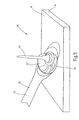
- FIG. 2 shows a first embodiment of a contact point.
- FIG. 3 shows a second embodiment of a contact point.
- FIG. 4 shows a third embodiment of a contact point.
- FIG. 5 shows a fourth embodiment of a contact point.
- FIG. 6 shows a fifth embodiment of a contact point.
- FIG. 1 a shows an electrical connection 10 between a first contact surface 12 and a second contact surface 14 .
- Contact surface 12 is provided on a substrate 16 and contact surface 14 on a substrate 18 .
- Electrical connection 10 is produced by bonding in the known manner (ball-wedge bonding).
- a wire-bonding tool (not illustrated) is used to first heat the free end of a contact wire 20 , forming it into a ball 21 .
- a capillary nozzle of the wire-bonding tool is then used to press this ball 21 onto first contact surface 12 , thus producing atomic bonding forces at the boundary between what is then a plastically deformed ball 21 and contact surface 12 .
- the wire-bonding tool is then moved toward second contact surface 14 , thus forming a loop 22 in contact wire 20 .
- Contact wire 20 is pressed with the capillary nozzle onto second contact surface 14 , where it is plastically deformed, thus producing atomic bonding forces between contact wire 20 and second contact surface 14 .
- the plastic deformation of contact wire 20 (stitch) by the capillary nozzle simultaneously creates a rupture point at which contact wire 20 breaks after the capillary nozzle is removed.
- the design of second contact point 24 (wedge) has a relatively small contact area between contact wire 20 and contact surface 14 . As a result, contact point 24 allows contact wire 20 to pull away from contact surface 14 . Enormous contact problems arise, especially if contact surface 14 is made of a hard-to-bond material.
- Electrical connection 10 illustrated in FIG. 1 a is produced by a known bonding method (ball-wedge method). Such electrical connections 10 are established, for example, when microhybrid components are connected to microchips.
- FIGS. 1 b to 1 h illustrate the method according to the present invention for establishing electrical connection 10 , with this method being based on an electrical connection previously established according to FIG. 1 a .
- identical components are always identified by the same reference numbers as in FIG. 1 a and are not explained again.
- FIG. 1 b shows a schematic representation of a capillary nozzle 26 of a wire-bonding tool 28 .
- Capillary nozzle 26 has a passage 30 through which contact wire 20 is fed. Suitable feed devices enable contact wire 20 to move through capillary nozzle 26 .
- contact wire 20 moves toward second contact surface 14 , and its free end 32 is heated to a temperature above its melting point, using a thermal energy source.
- a surface tension causes the molten mass of contact wire 20 to form a ball 34 . Melting a ball 34 onto end 32 takes place directly after establishing the connection between contact wire 20 and contact surface 14 , as shown in FIG. 1 a . As a result, it is not necessary to reposition capillary nozzle 26 in relation to contact point 24 .
- capillary nozzle 26 According to the next process step illustrated in FIG. l c , a force and ultrasound are applied to capillary nozzle 26 . This compresses ball 34 , which undergoes plastic deformation.
- the shape of capillary nozzle 26 can influence the plastic deformation of ball 34 .
- the end of capillary nozzle 26 facing contact surface 14 has a circumferential ring-shaped ridge 36 that engages with an inner cone 38 .
- capillary nozzle 26 is moved laterally away from contact point 24 . This movement is indicated by an arrow 40 . If necessary, lateral movement 40 can be superimposed on the lifting of capillary nozzle 26 away from contact point 24 ( FIG. 1 d ). Movement 40 is oriented so that its direction vector is more or less contrary to a longitudinal extension of contact wire 20 laid in loop 22 . Direction of movement 40 is maintained until a vertex 44 of ring-shaped ridge 26 of capillary nozzle 26 has passed 10 an imaginary perpendicular running through deformed ball 34 (perpendicular that is parallel to the axis of capillary nozzle 26 ). As shown in FIG.
- capillary nozzle 26 is moved in the direction of contact surface 14 so that ring-shaped ridge 36 strikes plastically deformed ball 34 .
- ball 34 undergoes a further plastic deformation, due to the outer lateral surface of ring-shaped ridge 36 .
- Ball 34 undergoes a segment-like deformation.
- Ball 34 continues to change shape until segment 34 ′ projects laterally over contact wire 20 already bonded to contact surface 14 and comes into physical contact with contact surface 14 in additional bonding areas 48 . This type of deformation generates atomic bonding forces between segment 34 ′ formed and contact surface 14 , causes the segment to permanently adhere to the surface.
- segment 34 spans contact wire 20 in the area of contact point 24 and holds the latter in place like a strap, as shown in FIG. 1 g .
- Segment 34 provides a kind of tensile strain relief function to secure contact point 24 for contact wire 20 .
- the remaining wire that broke away when capillary nozzle 26 was removed is visible in center 40 of contact point 24 in the form of a pointed elevation 50 .
- the latter forms an additional positive-lock joint with contact wire 20 in the area of contact point 24 .
- FIG. 1 h shows an enlarged representation of contact point 24 after electrical connection 10 has been established with additional contact securing provided by segment 34 ′.
- segment 34 ′ has certain shape characteristics that are derived from the size of ball 34 ( FIG. 1 b ), the size and type of bonding parameters ( FIG. 1 f ), and the shape of ring-shaped ridge 36 of capillary nozzle 26 . Because the shape of capillary nozzle 26 , the magnitude of bonding forces, and the size of ball 34 are known or can be set, segments 34 ′ can be achieved in reproducible shapes. After contact point 24 has been produced, segment 34 ′ can be measured by an optical monitoring unit (not illustrated).
- segment 34 ′ different shapes can be selected for segment 34 ′.
- FIGS. 2 through 6 show different embodiments of segment 34 ′.
- the shape of segment 34 ′ can be selected, for example, by choosing a different shape for capillary nozzle 26 and varying the placement of capillary nozzle 26 when shaping ball 34 into segment 34 ′.
- the design of segment 34 , and the way it bonds to contact surface 14 can be influenced by setting general bonding parameters, such as force F or the frequency and intensity of the ultrasound energy.
- FIG. 2 shows a segment 34 ′ that is designed in the shape of a ridge.
- segment 34 ′ in FIG. 3 has a flatter design and merges with the material of tip 50 .
- segment 34 ′ has an even flatter design, so that it is almost shaped like a disk and also merges with the material of tip 50 .
- FIG. 5 shows a further embodiment, in which segment 34 ′ is shaped like a shallow basin, with segment 34 ′ again merging with the material of tip 50 .
- FIG. 6 shows an embodiment of segment 34 ′ in which segment 34 ′ is designed as a largely flat disk that has a ridge-shaped bulge in the direction of contact wire 20 .
- Tip 50 in this case, is formed from the material of segment 34 ′ by deforming ball 34 accordingly. This can be achieved by a suitable design of capillary nozzle 26 and placement of capillary nozzle 26 while forming the ball into segment 34 ′.
- segment 34 ′ it is also possible to modulate segment 34 ′ as a largely rectangular object having a defined elongation in the x-direction, y-direction, and z-direction by setting the bonding parameters and/or placement parameters of capillary nozzle 26 while shaping segment 34 ′.
- Parameters that can be set while shaping ball 34 into “rectangular” segment 34 ′ make it possible to set precisely reproducible dimensions in the x-, y-, and z-directions.
- a subsequent visual, in particular automatic visual, inspection of contact point 24 can be used to easily and effectively check contact point 24 for freedom from errors.
Abstract
A method for establishing an electrical connection between a first contact surface and a second contact surface, with a wire-bonding tool being used to provide a contact wire between the contact surfaces by bonding the contact wire to the first contact surface and subsequently leading it to the second contact surface, bonding it to the latter, and subsequently, separating it using the wire-bonding tool. After the contact wire has been separated from the second contact surface, the wire-bonding tool is used to provide the contact point with an additional contact securing element via the contact wire.
Description
This application is a divisional of prior application Ser. No. 10/251,417 now U.S. Pat. No. 7,083,077 filed Sep. 20, 2002 which is a divisional of prior application Ser. No. 09/701,224 now U.S. Pat. No. 6,477,768 filed Mar. 12, 2001.
The present invention relates to a method for establishing an electrical connection, features and a contact point.
A single-wire contacting method, called bonding, is known for establishing an electrical connection between at least two contact surfaces. In doing this, individual wires, in particular, gold or aluminum wires, are positioned between the contact surfaces to be bonded, using a wire-bonding tool. In bonding, the contact wire is bonded to the contact surfaces by applying ultrasonic pressure and heat. The free end of the bonding wire is first melted to form a ball, by applying thermal energy, and subsequently pressed onto the first contact surface, using a bonding capillary. The contact wire bonds to the contact surface as a result of atomic bonding forces (material fusion) arising at the boundary between the contact surface and the contact wire. During bonding to the first contact surface, the ball that was previously melted on is deformed into a nail head. The contact wire is then led to the second contact surface, using the wire-bonding tool. To prevent the contact wire from breaking away at the first contact point, the contact wire is formed into a loop. The contact wire is then pressed onto the second contact surface with the wire-bonding tool by again applying ultrasonic pressure and heat. This produces necking of the contact wire, causing the latter to form a rupture joint at which the contact wire breaks away from the second contact surface as the wire-bonding tool moves on. The contact wire is bonded to the second contact surface by a “stitch,” with atomic bonding forces again arising at the boundary between the contact wire and the second contact surface.
This known ball-wedge bonding method (ball bonding with the first contact surface, and stitch bonding with the second contact surface) produces a strong dependency between the materials of the contact wire and the contact surface, thus forming strong atomic bonding forces at the boundaries. Particularly when contacting the second contact surface, a relatively weak surface bonding forms between the stitch and the contact surface, resulting in contacting errors, particularly in the case of contact surfaces made of hard-to-bond materials.
The method according to the present invention offers an advantage over the related art in that it considerably improves the contact stability of the bond between the contact wire and the second contact surface. The fact that the wire-bonding tool provides the contact point with an additional contact securing element after bonding the second contact surface increases the contact stability of the second contact point (stitch or wedge) independently of the generation of atomic bonding force between the contact wire and the second contact surface.
In one preferred embodiment of the present invention, the additional contact securing element is provided by the ball shape, applied to the contact point and subsequently deformed by the bonding tool, at the end of the contact wire that remains free after contacting the second contact surface. This makes it possible, after forming the electrical connection between the contact wire and the second contact surface, to immediately form the ball on the end of the contact wire that is now free and to position it over the contact point as an additional contact securing element. A particularly preferred feature is to deform the ball with the wire-bonding tool so that the contact point overlaps, producing at least one, preferably two, additional bonding areas between the additional contact securing element and the contact surface. The atomic bonding forces generated cause the additional bonding areas to adhere to the contact surface, forming a sort of tensile strain relief for the contact wire bonded to the second contact surface. This very reliably prevents the contact wire from breaking away from the second contact surface. The possibility of the contact wire breaking away is now determined only by the rupture strength of the contact wire itself, and no longer by the adhesion between the contact wire and the second contact surface, i.e., the contact wire itself breaks before the contact point ruptures.
According to another preferred embodiment of the present invention, the production of the additional contact securing element can be precisely reproduced through wire-bonding tool settings, in particular, by programming a corresponding controller of the wire-bonding tool. This makes it possible to create identical contact securing elements among a large number of contacts, and these identical contact securing elements can be easily tested on the basis of a predictable, reproducible result. One particularly preferred feature is that a visual, preferably automatic visual, inspection of the contact point is carried out, in which the contact securing elements that are not precisely produced, i.e., according to the specified degree of reproducibility, are reliably detected. This makes it possible to achieve a sort of zero error rate in producing bonds that result in a higher production yield.
A contact point according to the present invention advantageously ensures a high contact stability between the contact wire and contact surface. Since the contact point includes an additional contact securing element which at least partially engages over the contact wire in the area of the contact point and forms at least one additional bonding surface with the contact surface, the available overall surface is advantageously increased for contacting the contact wire with the contact surface, enabling the contact point to withstand higher mechanical stresses. Particularly when used in safety-related components, this contact point can maintain highly redundant electrical connections.
According to the next process step illustrated in FIG. lc, a force and ultrasound are applied to capillary nozzle 26. This compresses ball 34, which undergoes plastic deformation. The shape of capillary nozzle 26 can influence the plastic deformation of ball 34. In the illustrated embodiment, the end of capillary nozzle 26 facing contact surface 14 has a circumferential ring-shaped ridge 36 that engages with an inner cone 38.
The plastic deformation of ball 34 follows the shape of this inner cone 38. The application of contact force F, combined with ultrasound energy, produces atomic bonding forces between ball 34 and, extending from center 40 of bonding point 24 to the wedge, causing deformed ball 34 adhere to contact point 24 during a motion away from contact surface 14, as shown in FIG. 1 d.
In a subsequent process step, illustrated in FIG. 1 e, capillary nozzle 26 is moved laterally away from contact point 24. This movement is indicated by an arrow 40. If necessary, lateral movement 40 can be superimposed on the lifting of capillary nozzle 26 away from contact point 24 (FIG. 1 d). Movement 40 is oriented so that its direction vector is more or less contrary to a longitudinal extension of contact wire 20 laid in loop 22. Direction of movement 40 is maintained until a vertex 44 of ring-shaped ridge 26 of capillary nozzle 26 has passed 10 an imaginary perpendicular running through deformed ball 34 (perpendicular that is parallel to the axis of capillary nozzle 26). As shown in FIG. 1 f, capillary nozzle 26 is moved in the direction of contact surface 14 so that ring-shaped ridge 36 strikes plastically deformed ball 34. Depending on contact force F′ applied, and under the influence of ultrasound, ball 34 undergoes a further plastic deformation, due to the outer lateral surface of ring-shaped ridge 36. Ball 34 undergoes a segment-like deformation. Ball 34 continues to change shape until segment 34′ projects laterally over contact wire 20 already bonded to contact surface 14 and comes into physical contact with contact surface 14 in additional bonding areas 48. This type of deformation generates atomic bonding forces between segment 34′ formed and contact surface 14, causes the segment to permanently adhere to the surface. After capillary nozzle 26 moves away, segment 34 spans contact wire 20 in the area of contact point 24 and holds the latter in place like a strap, as shown in FIG. 1 g. Segment 34 provides a kind of tensile strain relief function to secure contact point 24 for contact wire 20. The remaining wire that broke away when capillary nozzle 26 was removed is visible in center 40 of contact point 24 in the form of a pointed elevation 50. The latter forms an additional positive-lock joint with contact wire 20 in the area of contact point 24.
The present invention is, of course, not limited to the embodiment illustrated in FIG. 1 . In particular, different shapes can be selected for segment 34′. FIGS. 2 through 6 show different embodiments of segment 34′. The shape of segment 34′ can be selected, for example, by choosing a different shape for capillary nozzle 26 and varying the placement of capillary nozzle 26 when shaping ball 34 into segment 34′. In addition, the design of segment 34, and the way it bonds to contact surface 14, can be influenced by setting general bonding parameters, such as force F or the frequency and intensity of the ultrasound energy.
According to further exemplary embodiments, it is possible, in particular, to provide a more shallow depression between tip 50 and segment 34′. This means that the transition between segment 34′ and point 50 occurs through a relatively shallow depression, thereby improving the positive-lock joint between contact wire 20 and segment 34′ or contact point 24 in the example.
By way of example, FIG. 2 shows a segment 34′ that is designed in the shape of a ridge. In contrast to this, segment 34′ in FIG. 3 has a flatter design and merges with the material of tip 50. According to the embodiment illustrated in FIG. 4 , segment 34′ has an even flatter design, so that it is almost shaped like a disk and also merges with the material of tip 50. FIG. 5 shows a further embodiment, in which segment 34′ is shaped like a shallow basin, with segment 34′ again merging with the material of tip 50. Finally, FIG. 6 shows an embodiment of segment 34′ in which segment 34′ is designed as a largely flat disk that has a ridge-shaped bulge in the direction of contact wire 20. Tip 50, in this case, is formed from the material of segment 34′ by deforming ball 34 accordingly. This can be achieved by a suitable design of capillary nozzle 26 and placement of capillary nozzle 26 while forming the ball into segment 34′.
It is also possible to modulate segment 34′ as a largely rectangular object having a defined elongation in the x-direction, y-direction, and z-direction by setting the bonding parameters and/or placement parameters of capillary nozzle 26 while shaping segment 34′. Parameters that can be set while shaping ball 34 into “rectangular” segment 34′ make it possible to set precisely reproducible dimensions in the x-, y-, and z-directions. A subsequent visual, in particular automatic visual, inspection of contact point 24 can be used to easily and effectively check contact point 24 for freedom from errors.
Claims (10)
1. A contact point for bonding a contact wire to a contact surface, with the contact wire merging with a material of the contact surface, comprising:
a first contact securing element forming a first bonding area within the contact surface;
an additional contact securing element that is directly attached to the first contact securing element, at least partially engages over the contact wire in an area of the contact point and forms at least one additional bonding area with the contact surface, wherein the additional contact securing element is coterminous with, and formed from the same material as, the first contact securing element; and
a positive lock joint located within a surface area of the additional contact securing element;
wherein the additional contact securing element includes a segment that engages with a stitch of the contact wire at the contact point and is positioned on one side of a center of the contact point in a direction of a loop of the contact wire, and
wherein the additional contact securing element includes a ridge-shaped structure substantially on one side and in the direction of the loop of the contact wire, and extending away from a center of the additional contact securing element.
2. The contact point as recited in claim 1 , wherein the segment engages with both sides of the contact wire to form the at least one additional bonding area with the contact surface.
3. The contact point as recited in claim 1 , wherein the segment has a rectangular shape with dimensions in the x-, y-, and z-directions that can be reproducibly set using a wire-bonding tool.
4. The contact point as recited in claim 1 , wherein the lock joint forms an elevated tip extending away from the contact surface.
5. The contact point as recited in claim 1 , wherein the additional contact securing element is substantially disk-shaped.
6. The contact point as recited in claim 1 , wherein the additional contact securing element includes a concavity located between a ridge portion of the additional contact securing element and a pointed elevation portion of the additional contact securing element.
7. The contact point as recited in claim 1 , wherein a peripheral portion of the additional contact securing element forms a ridge-shaped bulge extending towards an opposing end of the contact wire.
8. The contact point as recited in claim 1 , wherein the additional contact securing element includes a segment that engages with a stitch of the contact wire at the contact point and is positioned on one side of a center of the contact point in a direction of a loop of the contact wire, and wherein the lock joint forms an elevated tip extending away from the contact surface.
9. The contact point as recited in claim 1 , wherein the additional contact securing element includes a segment that engages with a stitch of the contact wire at the contact point and is positioned on one side of a center of the contact point in a direction of a loop of the contact wire, and wherein the additional contact securing element is substantially disk-shaped.
10. A contact point arrangement for bonding a contact wire to a contact surface, comprising:
a substantially flattened section of the contact wire, the flattened section adhering directly to the contact surface to form a stitch bond;
a ridge-shaped portion formed from an additional piece of wire material melded to the flattened section, the ridge-shaped portion projecting from the flattened section at an angle away from the contact surface; and
a pointed elevation formed from the additional piece of wire material, the pointed elevation being melded to, and projecting away from, a flat portion of the flattened section, wherein the ridge-shaped portion is substantially on one side and in the direction of a loop of the contact wire.
Priority Applications (1)
| Application Number | Priority Date | Filing Date | Title |
|---|---|---|---|
| US11/436,794 US7906858B2 (en) | 1998-05-27 | 2006-05-17 | Contact securing element for bonding a contact wire and for establishing an electrical connection |
Applications Claiming Priority (7)
| Application Number | Priority Date | Filing Date | Title |
|---|---|---|---|
| DE19823623A DE19823623A1 (en) | 1998-05-27 | 1998-05-27 | Method and contact point for establishing an electrical connection |
| DE19823623.9 | 1998-05-27 | ||
| DE19823623 | 1998-05-27 | ||
| US09/701,224 US6477768B1 (en) | 1998-05-27 | 1999-04-07 | Method and contact point for establishing an electrical connection |
| PCT/DE1999/001037 WO1999062114A1 (en) | 1998-05-27 | 1999-04-07 | Method and contact point for producing a wire bonding connection |
| US10/251,417 US7083077B2 (en) | 1998-05-27 | 2002-09-20 | Method and contact point for establishing an electrical connection |
| US11/436,794 US7906858B2 (en) | 1998-05-27 | 2006-05-17 | Contact securing element for bonding a contact wire and for establishing an electrical connection |
Related Parent Applications (1)
| Application Number | Title | Priority Date | Filing Date |
|---|---|---|---|
| US10/251,417 Division US7083077B2 (en) | 1998-05-27 | 2002-09-20 | Method and contact point for establishing an electrical connection |
Publications (2)
| Publication Number | Publication Date |
|---|---|
| US20060208038A1 US20060208038A1 (en) | 2006-09-21 |
| US7906858B2 true US7906858B2 (en) | 2011-03-15 |
Family
ID=7869032
Family Applications (3)
| Application Number | Title | Priority Date | Filing Date |
|---|---|---|---|
| US09/701,224 Expired - Fee Related US6477768B1 (en) | 1998-05-27 | 1999-04-07 | Method and contact point for establishing an electrical connection |
| US10/251,417 Expired - Lifetime US7083077B2 (en) | 1998-05-27 | 2002-09-20 | Method and contact point for establishing an electrical connection |
| US11/436,794 Expired - Lifetime US7906858B2 (en) | 1998-05-27 | 2006-05-17 | Contact securing element for bonding a contact wire and for establishing an electrical connection |
Family Applications Before (2)
| Application Number | Title | Priority Date | Filing Date |
|---|---|---|---|
| US09/701,224 Expired - Fee Related US6477768B1 (en) | 1998-05-27 | 1999-04-07 | Method and contact point for establishing an electrical connection |
| US10/251,417 Expired - Lifetime US7083077B2 (en) | 1998-05-27 | 2002-09-20 | Method and contact point for establishing an electrical connection |
Country Status (5)
| Country | Link |
|---|---|
| US (3) | US6477768B1 (en) |
| EP (1) | EP1080491B1 (en) |
| JP (1) | JP4382281B2 (en) |
| DE (2) | DE19823623A1 (en) |
| WO (1) | WO1999062114A1 (en) |
Families Citing this family (26)
| Publication number | Priority date | Publication date | Assignee | Title |
|---|---|---|---|---|
| DE19831550B4 (en) * | 1998-07-14 | 2013-08-14 | Robert Bosch Gmbh | bonding process |
| JP3407275B2 (en) * | 1998-10-28 | 2003-05-19 | インターナショナル・ビジネス・マシーンズ・コーポレーション | Bump and method of forming the same |
| DE10065722B9 (en) * | 2000-12-29 | 2004-09-09 | Robert Bosch Gmbh | Method for making an electrical connection and device with an electrical connection |
| US20020195268A1 (en) * | 2001-06-21 | 2002-12-26 | Schendel Robert E. | Thick film circuit connection |
| US7249702B2 (en) | 2003-12-04 | 2007-07-31 | Kulicke And Soffa Industries, Inc. | Multi-part capillary |
| US20060206200A1 (en) | 2004-05-25 | 2006-09-14 | Chestnut Medical Technologies, Inc. | Flexible vascular occluding device |
| EP2419048A4 (en) | 2004-05-25 | 2014-04-09 | Covidien Lp | Vascular stenting for aneurysms |
| US8628564B2 (en) | 2004-05-25 | 2014-01-14 | Covidien Lp | Methods and apparatus for luminal stenting |
| EP2626038B1 (en) | 2004-05-25 | 2016-09-14 | Covidien LP | Flexible vascular occluding device |
| US8016182B2 (en) * | 2005-05-10 | 2011-09-13 | Kaijo Corporation | Wire loop, semiconductor device having same and wire bonding method |
| JP4530975B2 (en) * | 2005-11-14 | 2010-08-25 | 株式会社新川 | Wire bonding method |
| US8152833B2 (en) | 2006-02-22 | 2012-04-10 | Tyco Healthcare Group Lp | Embolic protection systems having radiopaque filter mesh |
| JP4694405B2 (en) * | 2006-04-12 | 2011-06-08 | ローム株式会社 | Wire bonding method |
| US8505805B2 (en) * | 2008-10-09 | 2013-08-13 | Honeywell International Inc. | Systems and methods for platinum ball bonding |
| DE102010030966B4 (en) * | 2010-07-06 | 2012-04-19 | Continental Automotive Gmbh | Electrically conductive connection between two contact surfaces |
| US20120288684A1 (en) * | 2011-05-12 | 2012-11-15 | Ming-Teng Hsieh | Bump structure and fabrication method thereof |
| US9443797B2 (en) | 2012-09-14 | 2016-09-13 | STATS ChipPAC Pte. Ltd. | Semiconductor device having wire studs as vertical interconnect in FO-WLP |
| US10192796B2 (en) | 2012-09-14 | 2019-01-29 | STATS ChipPAC Pte. Ltd. | Semiconductor device and method of forming dual-sided interconnect structures in FO-WLCSP |
| US9818734B2 (en) | 2012-09-14 | 2017-11-14 | STATS ChipPAC Pte. Ltd. | Semiconductor device and method of forming build-up interconnect structures over a temporary substrate |
| US9114001B2 (en) | 2012-10-30 | 2015-08-25 | Covidien Lp | Systems for attaining a predetermined porosity of a vascular device |
| US9452070B2 (en) * | 2012-10-31 | 2016-09-27 | Covidien Lp | Methods and systems for increasing a density of a region of a vascular device |
| US9943427B2 (en) | 2012-11-06 | 2018-04-17 | Covidien Lp | Shaped occluding devices and methods of using the same |
| SG11201503849YA (en) * | 2012-11-16 | 2015-06-29 | Shinkawa Kk | Wire-bonding apparatus and method of manufacturing semiconductor device |
| US9157174B2 (en) | 2013-02-05 | 2015-10-13 | Covidien Lp | Vascular device for aneurysm treatment and providing blood flow into a perforator vessel |
| TWI541920B (en) * | 2013-07-23 | 2016-07-11 | 矽品精密工業股份有限公司 | Method of manufacturing wire-bonding structure |
| US9893017B2 (en) | 2015-04-09 | 2018-02-13 | STATS ChipPAC Pte. Ltd. | Double-sided semiconductor package and dual-mold method of making same |
Citations (26)
| Publication number | Priority date | Publication date | Assignee | Title |
|---|---|---|---|---|
| US3373481A (en) | 1965-06-22 | 1968-03-19 | Sperry Rand Corp | Method of electrically interconnecting conductors |
| US3623649A (en) | 1969-06-09 | 1971-11-30 | Gen Motors Corp | Wedge bonding tool for the attachment of semiconductor leads |
| JPS5712530A (en) | 1980-06-27 | 1982-01-22 | Hitachi Ltd | Wire bonding method |
| US4415115A (en) | 1981-06-08 | 1983-11-15 | Motorola, Inc. | Bonding means and method |
| JPS59195836A (en) | 1983-04-21 | 1984-11-07 | Sony Corp | Wire bonding method |
| JPS61280626A (en) | 1985-05-08 | 1986-12-11 | Sanyo Electric Co Ltd | Wire-bonding |
| JPS63244633A (en) | 1987-03-31 | 1988-10-12 | Oki Electric Ind Co Ltd | Wire bonding method |
| JPS6457725A (en) | 1987-08-28 | 1989-03-06 | Taiyo Yuden Kk | Wire bonding method |
| JPH01158742A (en) | 1987-12-16 | 1989-06-21 | Sanken Electric Co Ltd | Manufacture of device with fine leads |
| JPH01239861A (en) | 1988-03-18 | 1989-09-25 | Shinkawa Ltd | Wire bonding |
| JPH01276729A (en) | 1988-04-28 | 1989-11-07 | Nec Kansai Ltd | Wire bonding |
| JPH03289149A (en) | 1990-04-05 | 1991-12-19 | Matsushita Electric Ind Co Ltd | Bonding method of wire |
| US5111989A (en) | 1991-09-26 | 1992-05-12 | Kulicke And Soffa Investments, Inc. | Method of making low profile fine wire interconnections |
| US5172851A (en) | 1990-09-20 | 1992-12-22 | Matsushita Electronics Corporation | Method of forming a bump electrode and manufacturing a resin-encapsulated semiconductor device |
| US5176310A (en) | 1988-11-28 | 1993-01-05 | Hitachi, Ltd. | Method and apparatus for wire bond |
| US5421503A (en) | 1994-08-24 | 1995-06-06 | Kulicke And Soffa Investments, Inc. | Fine pitch capillary bonding tool |
| US5476211A (en) | 1993-11-16 | 1995-12-19 | Form Factor, Inc. | Method of manufacturing electrical contacts, using a sacrificial member |
| JPH088284A (en) * | 1994-06-20 | 1996-01-12 | Hitachi Ltd | Wire bonding structure and its reinforcement method |
| US5836071A (en) | 1996-12-26 | 1998-11-17 | Texas Instrument Incorporated | Method to produce known good die using temporary wire bond, die attach and packaging |
| US5960262A (en) * | 1997-09-26 | 1999-09-28 | Texas Instruments Incorporated | Stitch bond enhancement for hard-to-bond materials |
| US6079610A (en) | 1996-10-07 | 2000-06-27 | Denso Corporation | Wire bonding method |
| US6158647A (en) | 1998-09-29 | 2000-12-12 | Micron Technology, Inc. | Concave face wire bond capillary |
| US6270000B1 (en) | 1999-03-02 | 2001-08-07 | Kabushiki Kaisha Shinkawa | Wire bonding method |
| US6295729B1 (en) | 1992-10-19 | 2001-10-02 | International Business Machines Corporation | Angled flying lead wire bonding process |
| US6316838B1 (en) | 1999-10-29 | 2001-11-13 | Fujitsu Limited | Semiconductor device |
| US6715666B2 (en) | 2002-08-08 | 2004-04-06 | Kaijo Corporation | Wire bonding method, method of forming bump and bump |
Family Cites Families (1)
| Publication number | Priority date | Publication date | Assignee | Title |
|---|---|---|---|---|
| US3622649A (en) * | 1969-08-15 | 1971-11-23 | Gulf Research Development Co | Dimerization of propylene to 2,3-dimethylbutenes |
-
1998
- 1998-05-27 DE DE19823623A patent/DE19823623A1/en not_active Withdrawn
-
1999
- 1999-04-07 WO PCT/DE1999/001037 patent/WO1999062114A1/en active IP Right Grant
- 1999-04-07 US US09/701,224 patent/US6477768B1/en not_active Expired - Fee Related
- 1999-04-07 EP EP99953402A patent/EP1080491B1/en not_active Expired - Lifetime
- 1999-04-07 DE DE59914827T patent/DE59914827D1/en not_active Expired - Lifetime
- 1999-04-07 JP JP2000551432A patent/JP4382281B2/en not_active Expired - Lifetime
-
2002
- 2002-09-20 US US10/251,417 patent/US7083077B2/en not_active Expired - Lifetime
-
2006
- 2006-05-17 US US11/436,794 patent/US7906858B2/en not_active Expired - Lifetime
Patent Citations (27)
| Publication number | Priority date | Publication date | Assignee | Title |
|---|---|---|---|---|
| US3373481A (en) | 1965-06-22 | 1968-03-19 | Sperry Rand Corp | Method of electrically interconnecting conductors |
| US3623649A (en) | 1969-06-09 | 1971-11-30 | Gen Motors Corp | Wedge bonding tool for the attachment of semiconductor leads |
| JPS5712530A (en) | 1980-06-27 | 1982-01-22 | Hitachi Ltd | Wire bonding method |
| US4415115A (en) | 1981-06-08 | 1983-11-15 | Motorola, Inc. | Bonding means and method |
| JPS59195836A (en) | 1983-04-21 | 1984-11-07 | Sony Corp | Wire bonding method |
| JPS61280626A (en) | 1985-05-08 | 1986-12-11 | Sanyo Electric Co Ltd | Wire-bonding |
| JPS63244633A (en) | 1987-03-31 | 1988-10-12 | Oki Electric Ind Co Ltd | Wire bonding method |
| JPS6457725A (en) | 1987-08-28 | 1989-03-06 | Taiyo Yuden Kk | Wire bonding method |
| JPH01158742A (en) | 1987-12-16 | 1989-06-21 | Sanken Electric Co Ltd | Manufacture of device with fine leads |
| JPH01239861A (en) | 1988-03-18 | 1989-09-25 | Shinkawa Ltd | Wire bonding |
| JPH01276729A (en) | 1988-04-28 | 1989-11-07 | Nec Kansai Ltd | Wire bonding |
| US5176310A (en) | 1988-11-28 | 1993-01-05 | Hitachi, Ltd. | Method and apparatus for wire bond |
| JPH03289149A (en) | 1990-04-05 | 1991-12-19 | Matsushita Electric Ind Co Ltd | Bonding method of wire |
| US5172851A (en) | 1990-09-20 | 1992-12-22 | Matsushita Electronics Corporation | Method of forming a bump electrode and manufacturing a resin-encapsulated semiconductor device |
| US5111989A (en) | 1991-09-26 | 1992-05-12 | Kulicke And Soffa Investments, Inc. | Method of making low profile fine wire interconnections |
| US6295729B1 (en) | 1992-10-19 | 2001-10-02 | International Business Machines Corporation | Angled flying lead wire bonding process |
| US5476211A (en) | 1993-11-16 | 1995-12-19 | Form Factor, Inc. | Method of manufacturing electrical contacts, using a sacrificial member |
| US5852871A (en) | 1993-11-16 | 1998-12-29 | Form Factor, Inc. | Method of making raised contacts on electronic components |
| JPH088284A (en) * | 1994-06-20 | 1996-01-12 | Hitachi Ltd | Wire bonding structure and its reinforcement method |
| US5421503A (en) | 1994-08-24 | 1995-06-06 | Kulicke And Soffa Investments, Inc. | Fine pitch capillary bonding tool |
| US6079610A (en) | 1996-10-07 | 2000-06-27 | Denso Corporation | Wire bonding method |
| US5836071A (en) | 1996-12-26 | 1998-11-17 | Texas Instrument Incorporated | Method to produce known good die using temporary wire bond, die attach and packaging |
| US5960262A (en) * | 1997-09-26 | 1999-09-28 | Texas Instruments Incorporated | Stitch bond enhancement for hard-to-bond materials |
| US6158647A (en) | 1998-09-29 | 2000-12-12 | Micron Technology, Inc. | Concave face wire bond capillary |
| US6270000B1 (en) | 1999-03-02 | 2001-08-07 | Kabushiki Kaisha Shinkawa | Wire bonding method |
| US6316838B1 (en) | 1999-10-29 | 2001-11-13 | Fujitsu Limited | Semiconductor device |
| US6715666B2 (en) | 2002-08-08 | 2004-04-06 | Kaijo Corporation | Wire bonding method, method of forming bump and bump |
Also Published As
| Publication number | Publication date |
|---|---|
| DE59914827D1 (en) | 2008-09-18 |
| JP2002517092A (en) | 2002-06-11 |
| JP4382281B2 (en) | 2009-12-09 |
| US20030019098A1 (en) | 2003-01-30 |
| EP1080491B1 (en) | 2008-08-06 |
| WO1999062114A1 (en) | 1999-12-02 |
| EP1080491A1 (en) | 2001-03-07 |
| US6477768B1 (en) | 2002-11-12 |
| US7083077B2 (en) | 2006-08-01 |
| DE19823623A1 (en) | 1999-12-02 |
| US20060208038A1 (en) | 2006-09-21 |
Similar Documents
| Publication | Publication Date | Title |
|---|---|---|
| US7906858B2 (en) | Contact securing element for bonding a contact wire and for establishing an electrical connection | |
| US6966480B2 (en) | Concave face wire bond capillary and method | |
| US5764486A (en) | Cost effective structure and method for interconnecting a flip chip with a substrate | |
| US5660319A (en) | Ultrasonic bonding process | |
| JP4787374B2 (en) | Semiconductor device manufacturing method and wire bonding apparatus | |
| US8815732B2 (en) | Wire bonding method and semiconductor device | |
| US5662261A (en) | Wire bonding capillary | |
| US5981371A (en) | Bump forming method | |
| JP2735022B2 (en) | Bump manufacturing method | |
| CA2252102A1 (en) | Two-step projecting bump for semiconductor chip and method for forming the same | |
| JPH1140598A (en) | Sealed type ball bonding equipment and method | |
| US6260753B1 (en) | Gold bumps bonding on connection pads and subsequent coining of their vertex | |
| US6182885B1 (en) | Wire bonding method | |
| KR20040034429A (en) | Method for determining optimum bond parameters when bonding with a wire bonder | |
| US6467677B1 (en) | Method and contact point for producing an electrical connection | |
| JPH01273325A (en) | Manufacture of capillary and semiconductor device using the capillary | |
| JPH01276729A (en) | Wire bonding | |
| JPH10303201A (en) | Capillary, its use method and bump formation device | |
| JP2000091372A (en) | Electronic component and capillary used for wire bonding the same | |
| JPH11186315A (en) | Wire-bonding device and manufacture of semiconductor device using thereof | |
| JPH11163027A (en) | Two-step wire bonding process | |
| JP4106140B2 (en) | Mounting method of semiconductor device | |
| JP2007027498A (en) | Method for manufacturing a semiconductor device and manufacturing equipment | |
| JPS60182730A (en) | Wire bonding method | |
| KR20060091622A (en) | Wire bonding method |
Legal Events
| Date | Code | Title | Description |
|---|---|---|---|
| STCF | Information on status: patent grant |
Free format text: PATENTED CASE |
|
| FPAY | Fee payment |
Year of fee payment: 4 |
|
| MAFP | Maintenance fee payment |
Free format text: PAYMENT OF MAINTENANCE FEE, 8TH YEAR, LARGE ENTITY (ORIGINAL EVENT CODE: M1552); ENTITY STATUS OF PATENT OWNER: LARGE ENTITY Year of fee payment: 8 |
|
| MAFP | Maintenance fee payment |
Free format text: PAYMENT OF MAINTENANCE FEE, 12TH YEAR, LARGE ENTITY (ORIGINAL EVENT CODE: M1553); ENTITY STATUS OF PATENT OWNER: LARGE ENTITY Year of fee payment: 12 |