US7909961B2 - Method and apparatus for photomask plasma etching - Google Patents
Method and apparatus for photomask plasma etching Download PDFInfo
- Publication number
- US7909961B2 US7909961B2 US11/554,495 US55449506A US7909961B2 US 7909961 B2 US7909961 B2 US 7909961B2 US 55449506 A US55449506 A US 55449506A US 7909961 B2 US7909961 B2 US 7909961B2
- Authority
- US
- United States
- Prior art keywords
- plate
- shield
- zones
- different
- apertures
- Prior art date
- Legal status (The legal status is an assumption and is not a legal conclusion. Google has not performed a legal analysis and makes no representation as to the accuracy of the status listed.)
- Expired - Fee Related, expires
Links
Images


Classifications
-
- H—ELECTRICITY
- H01—ELECTRIC ELEMENTS
- H01L—SEMICONDUCTOR DEVICES NOT COVERED BY CLASS H10
- H01L21/00—Processes or apparatus adapted for the manufacture or treatment of semiconductor or solid state devices or of parts thereof
- H01L21/02—Manufacture or treatment of semiconductor devices or of parts thereof
- H01L21/04—Manufacture or treatment of semiconductor devices or of parts thereof the devices having at least one potential-jump barrier or surface barrier, e.g. PN junction, depletion layer or carrier concentration layer
- H01L21/18—Manufacture or treatment of semiconductor devices or of parts thereof the devices having at least one potential-jump barrier or surface barrier, e.g. PN junction, depletion layer or carrier concentration layer the devices having semiconductor bodies comprising elements of Group IV of the Periodic System or AIIIBV compounds with or without impurities, e.g. doping materials
- H01L21/30—Treatment of semiconductor bodies using processes or apparatus not provided for in groups H01L21/20 - H01L21/26
- H01L21/302—Treatment of semiconductor bodies using processes or apparatus not provided for in groups H01L21/20 - H01L21/26 to change their surface-physical characteristics or shape, e.g. etching, polishing, cutting
- H01L21/306—Chemical or electrical treatment, e.g. electrolytic etching
- H01L21/3065—Plasma etching; Reactive-ion etching
-
- C—CHEMISTRY; METALLURGY
- C23—COATING METALLIC MATERIAL; COATING MATERIAL WITH METALLIC MATERIAL; CHEMICAL SURFACE TREATMENT; DIFFUSION TREATMENT OF METALLIC MATERIAL; COATING BY VACUUM EVAPORATION, BY SPUTTERING, BY ION IMPLANTATION OR BY CHEMICAL VAPOUR DEPOSITION, IN GENERAL; INHIBITING CORROSION OF METALLIC MATERIAL OR INCRUSTATION IN GENERAL
- C23F—NON-MECHANICAL REMOVAL OF METALLIC MATERIAL FROM SURFACE; INHIBITING CORROSION OF METALLIC MATERIAL OR INCRUSTATION IN GENERAL; MULTI-STEP PROCESSES FOR SURFACE TREATMENT OF METALLIC MATERIAL INVOLVING AT LEAST ONE PROCESS PROVIDED FOR IN CLASS C23 AND AT LEAST ONE PROCESS COVERED BY SUBCLASS C21D OR C22F OR CLASS C25
- C23F4/00—Processes for removing metallic material from surfaces, not provided for in group C23F1/00 or C23F3/00
-
- G—PHYSICS
- G03—PHOTOGRAPHY; CINEMATOGRAPHY; ANALOGOUS TECHNIQUES USING WAVES OTHER THAN OPTICAL WAVES; ELECTROGRAPHY; HOLOGRAPHY
- G03F—PHOTOMECHANICAL PRODUCTION OF TEXTURED OR PATTERNED SURFACES, e.g. FOR PRINTING, FOR PROCESSING OF SEMICONDUCTOR DEVICES; MATERIALS THEREFOR; ORIGINALS THEREFOR; APPARATUS SPECIALLY ADAPTED THEREFOR
- G03F1/00—Originals for photomechanical production of textured or patterned surfaces, e.g., masks, photo-masks, reticles; Mask blanks or pellicles therefor; Containers specially adapted therefor; Preparation thereof
- G03F1/68—Preparation processes not covered by groups G03F1/20 - G03F1/50
- G03F1/80—Etching
-
- H—ELECTRICITY
- H01—ELECTRIC ELEMENTS
- H01J—ELECTRIC DISCHARGE TUBES OR DISCHARGE LAMPS
- H01J37/00—Discharge tubes with provision for introducing objects or material to be exposed to the discharge, e.g. for the purpose of examination or processing thereof
- H01J37/32—Gas-filled discharge tubes
- H01J37/32009—Arrangements for generation of plasma specially adapted for examination or treatment of objects, e.g. plasma sources
- H01J37/32082—Radio frequency generated discharge
- H01J37/321—Radio frequency generated discharge the radio frequency energy being inductively coupled to the plasma
-
- H—ELECTRICITY
- H01—ELECTRIC ELEMENTS
- H01J—ELECTRIC DISCHARGE TUBES OR DISCHARGE LAMPS
- H01J37/00—Discharge tubes with provision for introducing objects or material to be exposed to the discharge, e.g. for the purpose of examination or processing thereof
- H01J37/32—Gas-filled discharge tubes
- H01J37/32009—Arrangements for generation of plasma specially adapted for examination or treatment of objects, e.g. plasma sources
- H01J37/32422—Arrangement for selecting ions or species in the plasma
Definitions
- Embodiments of the present invention generally relate to a method and apparatus for plasma etching photomasks and, more specifically, to a method and apparatus with improved control of distribution of plasma species.
- microelectronics or integrated circuit devices typically involves a complicated process sequence requiring hundreds of individual steps performed on semiconductive, dielectric and conductive substrates. Examples of these process steps include oxidation, diffusion, ion implantation, thin film deposition, cleaning, etching and lithography.
- lithography and etching (often referred to as pattern transfer steps), a desired pattern is first transferred to a photosensitive material layer, e.g., a photoresist, and then to the underlying material layer during subsequent etching.
- a blanket photoresist layer is exposed to a radiation source through a reticle or photomask containing a pattern so that an image of the pattern is formed in the photoresist.
- photoresist By developing the photoresist in a suitable chemical solution, portions of the photoresist are removed, thus resulting in a patterned photoresist layer.
- the underlying material layer With this photoresist pattern acting as a mask, the underlying material layer is exposed to a reactive environment, e.g., using wet or dry etching, which results in the pattern being transferred to the underlying material layer.
- the pattern on a photomask which is typically formed in a metal-containing layer supported on a glass or quartz substrate, is also generated by etching through a photoresist pattern.
- the photoresist pattern is created by a direct write technique, e.g., with an electron beam or other suitable radiation beam, as opposed to exposing the photoresist through a reticle.
- the pattern can be transferred to the underlying metal-containing layer using plasma etching.
- An example of a commercially available photomask etch equipment suitable for use in advanced device fabrication is the TetraTM Photomask Etch System, available from Applied Materials, Inc., of Santa Clara, Calif.
- the terms “mask”, “photomask” or “reticle” will be used interchangeably to denote generally a substrate containing a pattern.
- the present invention generally provides a method and apparatus for etching photomasks.
- One embodiment of the invention provides an apparatus for plasma etching, comprising a process chamber, a support pedestal disposed in the process chamber and adapted to receive a photomask, an RF power source for forming a plasma within the chamber, a shield disposed in the chamber above the pedestal, the shield comprising a plate having a plurality of apertures and configured to control the distribution of charged and neutral species passing through the plate, wherein the plate comprises two zones having at least one characteristic—that of material or potential bias, being different from each other.
- Another embodiment of the invention provides a method of etching a photomask.
- the method comprises providing a process chamber having a support pedestal; providing a shield above the support pedestal, the shield comprising a plate having a first zone and a second zone each comprising a plurality of apertures and configured to control a distribution of charged and neutral species passing through the plate, the first zone having at least one characteristic—that of material or potential bias, being different from the second zone, placing a photomask upon the pedestal, introducing a process gas into the process chamber, forming a plasma from the process gas, and etching the photomask with ions and neutral species that pass through the plate.
- the apparatus comprises a process chamber, a support pedestal disposed in the process chamber and adapted to receive a photomask, an RF power source for forming a plasma within the chamber, an RF power source for forming a plasma within the chamber, and a shield disposed in the chamber above the pedestal, the shield comprising a plate having a plurality of apertures and configured to control the distribution of charged and neutral species passing through the plate, wherein the plate comprises a material selected from the group consisting of yttria and a material having a dielectric constant higher than about 4.
- FIG. 1 is a schematic diagram of an etch reactor having a shield
- FIGS. 2A-B are schematic illustrations of the top views of two embodiments of the shield of FIG. 1 ;
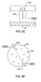
- FIG. 2C is a schematic cross-sectional view of a portion of the shield
- FIG. 2D is a schematic illustration of the top view of one embodiment showing a potential bias across the shield
- FIGS. 3A-B are schematic illustrations of the top views of two alternative embodiments of the shield
- FIG. 4 is a schematic illustration of a top view of another embodiment of the shield.
- FIG. 5 is a flow chart of a method of etching a photomask according to one embodiment of the invention.
- the present invention provides a method and apparatus for improving the etching of a photomask substrate. More specifically, the invention relates to an improved shield for controlling the spatial distribution of charged and neutral species in a plasma etch chamber. This shield is also referred to as an ion-radical or ion-neutral shield.
- FIG. 1 depicts a schematic diagram of an etch reactor 100 having an ion-radical shield 170 .
- Suitable reactors that may be adapted for use with the teachings disclosed herein include, for example, the Decoupled Plasma Source (DPS®) II reactor, or the Tetra I and Tetra II Photomask etch systems, all of which are available from Applied Materials, Inc. of Santa Clara, Calif.
- DPS® Decoupled Plasma Source
- Tetra I and Tetra II Photomask etch systems all of which are available from Applied Materials, Inc. of Santa Clara, Calif.
- the particular embodiment of the reactor 100 shown herein is provided for illustrative purposes and should not be used to limit the scope of the invention. It is contemplated that the invention may be utilized in other plasma processing chambers, including those from other manufacturers.
- the reactor 100 generally comprises a process chamber 102 having a substrate pedestal 124 within a conductive body (wall) 104 , and a controller 146 .
- the chamber 102 has a substantially flat dielectric ceiling or lid 108 .
- Other modifications of the chamber 102 may have other types of ceilings, e.g., a dome-shaped ceiling.
- An antenna 110 is disposed above the ceiling 108 and comprises one or more inductive coil elements that may be selectively controlled (two co-axial elements 110 a and 110 b are shown in FIG. 1 ).
- the antenna 110 is coupled through a first matching network 114 to a plasma power source 112 , which is typically capable of producing up to about 3000 W at a tunable frequency in a range from about 50 kHz to about 13.56 MHz.
- the substrate pedestal (cathode) 124 is coupled through a second matching network 142 to a biasing power source 140 .
- the biasing source 140 generally is a source of up to about 500 W at a frequency of approximately 13.56 MHz that is capable of producing either continuous or pulsed power.
- the source 140 may be a DC or pulsed DC source.
- the substrate support pedestal 124 comprises an electrostatic chuck 160 , which has at least one clamping electrode 132 and is controlled by a chuck power supply 166 .
- the substrate pedestal 124 may comprise substrate retention mechanisms such as a susceptor clamp ring, a mechanical chuck, and the like.
- a reticle adapter 182 is used to secure the substrate (e.g., mask or reticle) 122 onto the substrate support pedestal 124 .
- the reticle adapter 182 generally includes a lower portion 184 that covers an upper surface of the pedestal 124 (for example, the electrostatic chuck 160 ) and a top portion 186 having an opening 188 that is sized and shaped to hold the substrate 122 .
- the opening 188 is generally substantially centered with respect to the pedestal 124 .
- the adapter 182 is generally formed from a single piece of etch resistant, high temperature resistant material such as polyimide ceramic or quartz.
- An edge ring 126 may cover and/or secure the adapter 182 to the pedestal 124 .
- a lift mechanism 138 is used to lower or raise the adapter 182 , and hence, the substrate 122 , onto or off of the substrate support pedestal 124 .
- the lift mechanism 162 comprises a plurality of lift pins 130 (one lift pin is shown) that travel through respective guide holes 136 .
- the temperature of the substrate 122 is controlled by stabilizing the temperature of the substrate pedestal 124 .
- the substrate support pedestal 124 comprises a resistive heater 144 and a heat sink 128 .
- the resistive heater 144 generally comprises at least one heating element 134 and is regulated by a heater power supply 168 .
- a backside gas, e.g., helium (He) from a gas source 156 is provided via a gas conduit 158 to channels that are formed in the pedestal surface under the substrate 122 to facilitate heat transfer between the pedestal 124 and the substrate 122 .
- the pedestal 124 may be heated by the resistive heater 144 to a steady-state temperature, which in combination with the backside gas, facilitates uniform heating of the substrate 122 .
- the substrate 122 may be maintained at a temperature between about 0 and 350 degrees Celsius (0° C.).
- An ion-radical shield 170 is disposed in the chamber 102 above the pedestal 124 .
- the ion-radical shield 170 is electrically isolated from the chamber walls 104 and the pedestal 124 such that no ground path from the plate to ground is provided.
- One embodiment of the ion-radical shield 170 comprises a substantially flat plate 172 and a plurality of legs 176 supporting the plate 172 .
- the plate 172 which may be made of a variety of materials compatible with process needs, comprises one or more openings (apertures) 174 that define a desired open area in the plate 172 .
- This open area controls the amount of ions that pass from a plasma formed in an upper process volume 178 of the process chamber 102 to a lower process volume 180 located between the ion-radical shield 170 and the substrate 122 .
- the greater the open area the more ions can pass through the ion-radical shield 170 .
- the size of the apertures 174 controls the ion density in volume 180 , and the shield 170 serves as an ion filter.
- the plate 172 may also comprise a screen or a mesh wherein the open area of the screen or mesh corresponds to the desired open area provided by apertures 174 . Alternatively, a combination of a plate and screen or mesh may also be used.
- a potential develops on the surface of the plate 172 as a result of electron bombardment from the plasma.
- the potential attracts ions from the plasma, effectively filtering them from the plasma, while allowing neutral species, e.g., radicals, to pass through the apertures 174 of the plate 172 .
- neutral species e.g., radicals
- etching of the mask by neutral species or radicals can proceed in a more controlled manner. This reduces erosion of the resist as well as sputtering of the resist onto the sidewalls of the patterned material layer, thus resulting in improved etch bias and critical dimension uniformity.
- the present invention provides various enhancements to the ion-radical shield 170 , including alternative materials and configurations.
- using quartz or ceramics for the plate 172 may be beneficial over anodized aluminum, because it is believed that eddy currents may form in the aluminum plate and adversely affect process uniformity.
- the plate 172 is made of a material having a dielectric constant greater than about 4. Examples of such materials include ceramics, e.g., alumina, yttria (yttrium oxide), and K140 (a proprietary material available from Kyocera), among others.
- the ion-radical shield 170 comprises two zones or segments having at least one characteristic that is different from each other.
- the shield may comprise a number of zones with different configurations including various geometries (e.g., sizes, shapes and open areas), and the zones may be made of the same or different materials, or be adapted to have different potential bias.
- zone configurations, materials and/or potential bias By providing combinations of zone configurations, materials and/or potential bias, the spatial distribution of ions and neutrals in the plasma can be modified in a localized manner, allowing customization of process characteristics such as etch uniformity, or locally enhanced or reduced etch rates (e.g., to tailor to different pattern densities in different parts of a mask), and so on.
- Such a multi-zone shield for example, can be used for active control of plasma species distribution, and thus, allow for enhanced process control.
- At least two zones of the shield are made of different materials having different dielectric constants. Suitable materials include a variety of ceramics (e.g., alumina, yttria), anodized aluminum, quartz, materials with dielectric constant higher than about 4, e.g., K140 available from Kyocera, as well as other materials compatible with process chemistries.
- the shield is made primarily of one material, but is divided into different zones or segments that are physically separated or electrically isolated from each other. These zones are configured so that each can be independently biased to a different potential.
- the shield may comprise a plurality of zones having a combination of different geometric or spatial configurations, materials and/or potential biases.
- FIG. 2A is a schematic illustration of a top view of one embodiment of the shield 170 of the present invention.
- the shield 170 comprises a plate 172 having a plurality of apertures 174 and a plurality of legs 176 .
- the plate 172 is divided into different zones or segments 172 A, 172 B, 172 C and 172 D. At least two of these zones are made of different materials such as ceramic (e.g., alumina or yttria), quartz, anodized aluminum, or other materials compatible with process chemistries.
- ceramic e.g., alumina or yttria
- quartz e.g., alumina or yttria
- anodized aluminum e.g., aluminum
- the use of materials having different dielectric constants allows one to tune the plasma characteristics, and thus, the etch results. For example, a zone made of a higher dielectric constant material will result in a larger charge build-up compared to another zone made of a lower dielectric constant
- all the zones may also be made of the same material, and adjacent zones may be separated from each other by a gap 172 G or insulating material, as shown in FIG. 2B .
- adjacent zones may optionally be connected by one or more tabs 173 (made of a material different from the zones) to provide for mechanical stability, in addition to being supported by respective legs.
- one or more of the zones 172 A, 172 B, 172 C and 172 D may be connected to respective power sources for supplying a potential bias, which can be independently controlled for each zone.
- zone 172 A may be biased by power source 190 A at a different potential from zone 172 B, which is connected to another power source 190 B.
- the power source connection is illustrated in FIG.
- zone 172 A coupled to the substrate pedestal 124 by a leg 176 .
- the electrical connection from the power source 190 A is provided to the zone 172 A from inside the leg 176 .
- either positive or negative bias voltages can be applied to one of more zones.
- a DC bias voltage from about 0 volt to about 500 volt can be used.
- a DC bias voltage from about 0 volt to about 100 volt, or from about 0 volt to about 20 volt, may be used.
- zone 172 A For example, if a positive DC bias voltage is applied to the zone 172 A, and adjacent zones 172 B and 172 D are not biased (e.g., floating), positive ions repelled from zone 172 A will accumulate around zones 172 B and 172 D. This excess amount of positive ions, if not neutralized by the negative potentials built up from the electrons around zones 172 B and 172 D, will likely pass through the apertures 174 in these zones and contribute to the etching of the substrate 122 . Thus, by selectively biasing one or more zones on the plate 172 , the distribution of ions passing through the ion-neutral shield 170 can be varied in a controlled manner, resulting in corresponding changes in the etch results.
- the plate 172 comprises one material with a potential bias applied across two locations on the plate 172 .
- FIG. 2D in which two voltage sources 190 C and 190 D are connected to provide a potential gradient between locations 172 X and 172 Y.
- the potential gradient may be established across any two locations on the plate 172 .
- locations 172 X, 172 Y are disposed along diameter DD′ near the perimeter, on opposite sides of the center of the plate.
- the potential gradient may be applied between a first location near the center of the plate 172 , and a second location near the perimeter of the plate 172 .
- the distribution of ions and neutral species in the plasma passing through the apertures 174 of the plate 172 is modified by the potential gradient.
- FIGS. 3A-B are schematic illustrations of the top views of two embodiments of the shield 170 , showing different zones in various arrangements, e.g., 172 A and 172 B as concentric rings ( FIG. 3A ), and 172 A, 172 B, 172 C, 172 D, 172 E and 172 F in a grid or slice pattern ( FIG. 3B ).
- the concentric ring configuration may be useful in compensating for etch non-uniformities (in a radial direction) that may arise from non-uniform gas flow patterns in the chamber.
- each embodiment may be used in combination with each other, e.g., a plate, whether made of a single material or different materials, may comprise different zone configurations, or be provided with different potential bias across the plate.
- the apertures 174 in different zones of the plate 172 may vary in size, spacing and geometric arrangement.
- the apertures 174 may generally have dimensions ranging from 0.03 inches (0.07 cm) to about 3 inches (7.62 cm), and may be arranged to define an open area within each zone of the plate 172 from about 2 percent to about 90 percent. It is contemplated that apertures 174 may be arranged in other geometric or random patterns and with various dimensions.
- the size, shape and patterning of the apertures 174 may vary depending upon the desired ion density in the lower process volume 180 . For example, more apertures of small diameters in a particular zone of the plate 172 may be used to increase the radical (or neutral) to ion density ratio in a corresponding region of the volume 180 . Alternatively, a number of larger apertures may be interspersed with small apertures within a zone of the plate 172 to increase the ion to radical (or neutral) density ratio in a corresponding region of the volume 180 .
- FIGS. 2-3 are meant primarily for illustrative purposes, and it is understood that many different variations are possible, including combinations of zone configurations (e.g., sizes, shapes, open areas, materials and/or bias) that are designed to tailor to specific mask patterns so that process characteristics can be customized to suit specific needs. For example, if a mask has regions of different pattern densities or loading, the desired etch rates for these regions may be different from each other. In that case, it is possible to configure the zones or segments on the shield plate 172 based on the specific mask patterns in order to achieve the desired etch result.
- zones 172 A and 172 B illustrates a top view of one embodiment of plate 172 divided into zones 172 A and 172 B, whose spatial configurations correspond to or correlate with respective regions on a mask having different pattern densities.
- zone 172 A corresponds to a region on the mask requiring a relatively high etch rate than the rest of the mask
- zone 172 A may be provided with larger diameter apertures to provide for a higher ratio of ions to neutral species.
- zones 172 A and 172 B may be made of materials with different dielectric constants and/or biased differently such that the amount of ions (or ion to neutral ratio) passing through zone 172 A can be increased relatively to zone 172 B.
- the height at which the ion-radical shield 170 is supported may vary to further control the etch process.
- the ion-radical shield 170 is disposed approximately 1 inch (2.54 cm) from the ceiling 108 .
- a faster etch rate may be obtained by locating the ion-radical shield 170 closer to the pedestal 124 and, therefore, the substrate 122 .
- a lower, but more controlled, etch rate may be obtained by locating the ion-radical shield 170 farther from the pedestal 124 .
- the ion-radical shield 170 is disposed approximately 2 inches (5 cm) from the pedestal 124 .
- the height of the Ion-radical shield 170 may range from about 1.5 inches (3.81 cm) to about 4 inches (10.16 cm) in a chamber having a distance of about 6 inches (15.24 cm) between the substrate 122 and the ceiling 108 . It is contemplated that the ion-radical shield 170 may be positioned at different heights in chambers having different geometries, for example, larger or smaller chambers.
- the legs 176 which support the plate 172 in a spaced-apart relationship with respect to the substrate 122 , are generally located around an outer perimeter of the pedestal 124 or the edge ring 126 and may be fabricated of the same materials as the plate 172 . In one embodiment, three legs 176 are used to support the ion-radical shield 170 . Although the legs 176 generally maintain the plate 172 in a substantially parallel orientation relative to the substrate 122 or pedestal 124 , it is contemplated that an angled orientation may be used by having legs 176 of varied lengths.
- the legs 176 may be press fit at their upper ends into corresponding holes formed in the plate 172 , or they may be threaded into the plate 172 or into brackets secured to an underside of the plate 172 .
- the legs 176 may rest on the pedestal 124 , adapter 182 , or the edge ring 126 , or they may extend into receiving holes (not shown) formed in the pedestal 124 , adapter 182 , or edge ring 126 .
- Other conventional fastening methods not inconsistent with processing conditions may also be used, such as by screwing, bolting, bonding, among others.
- the ion-radical shield 170 When secured to the edge ring 126 , the ion-radical shield 170 may be part of an easily-replaceable process kit for ease of use, maintenance, replacement, and the like. It is contemplated that the ion-radical shield 170 may be configured to be easily retrofitted in existing process chambers.
- the plate 172 may be supported above the pedestal 124 by other means such as by using a bracket (not shown) attached to the wall 104 or other structure within the process chamber 102 . Where the plate 172 is attached to the wall 104 or other structure of the process chamber 102 , the plate 172 is generally insulated from any ground path such as the ground 106 .
- one or more process gases are provided to the process chamber 102 from a gas panel 120 , e.g., through one or more inlets 116 (e.g., openings, injectors, nozzles, and the like) located above the substrate pedestal 124 .
- the process gases are provided to the inlets 116 using an annular gas channel 118 , which may be formed in the wall 104 or in gas rings (as shown) that are coupled to the wall 104 .
- the process gases are ignited into a plasma by applying power from the plasma source 112 to the antenna 110 .
- the pressure in the chamber 102 is controlled using a throttle valve 162 and a vacuum pump 164 .
- the temperature of the wall 104 may be controlled using liquid-containing conduits (not shown) that run through the wall 104 .
- the chamber wall 104 is formed from a metal (e.g., aluminum, stainless steel, among others) and is coupled to an electrical ground 106 .
- the process chamber 102 also comprises conventional systems for process control, internal diagnostic, end point detection, and the like. Such systems are collectively shown as support systems 154 .
- the controller 146 comprises a central processing unit (CPU) 150 , a memory 148 , and support circuits 152 for the CPU 150 and facilitates control of the components of the process chamber 102 and, as such, of the etch process, as discussed below in further detail.
- the controller 146 may be one of any form of general-purpose computer processor that can be used in an industrial setting for controlling various chambers and sub-processors.
- the memory, or computer-readable medium, 642 of the CPU 150 may be one or more of readily available memory such as random access memory (RAM), read only memory (ROM), floppy disk, hard disk, or any other form of digital storage, local or remote.
- the support circuits 152 are coupled to the CPU 150 for supporting the processor in a conventional manner.
- circuits include cache, power supplies, clock circuits, input/output circuitry and subsystems, and the like.
- the inventive method is generally stored in the memory 148 as a software routine.
- such software routine may also be stored and/or executed by a second CPU (not shown) that is remotely located from the hardware being controlled by the CPU 150 .
- FIG. 5 illustrates a method 500 for etching a photomask substrate in an etch chamber having an ion-radical shield according to embodiments of the present invention.
- the method 500 begins at step 502 when the substrate is placed on a support pedestal beneath the ion-radical shield in a process chamber.
- the shield comprises two zones having at least one characteristic, e.g., material or potential bias, being different from each other.
- Typical substrates generally comprise an optically transparent silicon based material, such as quartz (i.e., silicon dioxide, SiO 2 ), having an opaque light-shielding layer of metal disposed on the surface of the quartz.
- Typical metals used in a photomask include chromium or chromium oxynitride.
- the substrate may also include a layer of silicon nitride (SiN) doped with molybdenum (Mo) interposed between the quartz and chromium.
- one or more process gases are introduced into the process chamber through a gas inlet.
- exemplary process gases may include oxygen (O 2 ) or an oxygen-containing gas, such as carbon monoxide (CO), and/or a halogen-containing gas, such as a chlorine-containing gas for etching the metal layer.
- the processing gas may further include an inert gas or another oxygen-containing gas.
- Carbon monoxide is advantageously used to form passivating polymer deposits on the surfaces, particularly the sidewalls, of openings and patterns formed in a patterned resist material and etched metal layers.
- Chlorine-containing gases are selected from the group of chlorine (Cl 2 ), silicon tetrachloride (SiCl 4 ), boron trichloride (BCl 3 ), and combinations thereof, and are used to supply reactive radicals to etch the metal layer.
- Cl 2 may be provided at a rate of 10 to 1000 standard cubic centimeters per minute (sccm), and O 2 may be provided at a rate of 0 to 1000 sccm.
- a substrate bias power between 5 and 500 W can be applied to the electrostatic chuck and the substrate maintained at a temperature below about 150° C.
- the pressure in the process chamber can be controlled between about 1 and about 40 mTorr.
- the process gases may comprise a fluorine-containing gas, e.g., trifluoromethane (CHF 3 ), tetrafluoromethane (CF 4 ), among others.
- a DC bias voltage is applied to at least one zone of the ion-radical shield.
- a plasma is formed from the one or more process gases in a process volume above the ion-radical shield, for example, by applying RF power between about 200 to about 2000 W from a plasma power source to an antenna. Ions and neutral species from the plasma pass through the ion-radical shield according to a distribution pattern determined by the potentials established by the applied bias voltage and the plasma across the ion-radical shield. The substrate is etched by the ions and neutral species in the lower process volume.
Abstract
Description
Claims (4)
Priority Applications (7)
| Application Number | Priority Date | Filing Date | Title |
|---|---|---|---|
| US11/554,495 US7909961B2 (en) | 2006-10-30 | 2006-10-30 | Method and apparatus for photomask plasma etching |
| CN201410178214.8A CN104035276B (en) | 2006-10-30 | 2007-08-08 | method and apparatus for photomask plasma etching |
| CNA2007101380582A CN101174106A (en) | 2006-10-30 | 2007-08-08 | Method and apparatus for photomask plasma etching |
| KR1020070086473A KR100951971B1 (en) | 2006-10-30 | 2007-08-28 | Method and apparatus for photomask plasma etching |
| TW096132787A TWI385709B (en) | 2006-10-30 | 2007-09-03 | Method and apparatus for photomask plasma etching |
| EP07020931.7A EP1918971B1 (en) | 2006-10-30 | 2007-10-25 | Method and apparatus for photomask plasma etching |
| JP2007279816A JP5421527B2 (en) | 2006-10-30 | 2007-10-29 | Photomask plasma etching method and apparatus |
Applications Claiming Priority (1)
| Application Number | Priority Date | Filing Date | Title |
|---|---|---|---|
| US11/554,495 US7909961B2 (en) | 2006-10-30 | 2006-10-30 | Method and apparatus for photomask plasma etching |
Publications (2)
| Publication Number | Publication Date |
|---|---|
| US20080099426A1 US20080099426A1 (en) | 2008-05-01 |
| US7909961B2 true US7909961B2 (en) | 2011-03-22 |
Family
ID=38927418
Family Applications (1)
| Application Number | Title | Priority Date | Filing Date |
|---|---|---|---|
| US11/554,495 Expired - Fee Related US7909961B2 (en) | 2006-10-30 | 2006-10-30 | Method and apparatus for photomask plasma etching |
Country Status (6)
| Country | Link |
|---|---|
| US (1) | US7909961B2 (en) |
| EP (1) | EP1918971B1 (en) |
| JP (1) | JP5421527B2 (en) |
| KR (1) | KR100951971B1 (en) |
| CN (2) | CN104035276B (en) |
| TW (1) | TWI385709B (en) |
Cited By (11)
| Publication number | Priority date | Publication date | Assignee | Title |
|---|---|---|---|---|
| US20100084980A1 (en) * | 2008-10-02 | 2010-04-08 | Bon-Woong Koo | Plasma uniformity control using biased array |
| US20130052811A1 (en) * | 2008-10-02 | 2013-02-28 | Varian Semiconductor Equipment Associates, Inc. | Plasma uniformity control using biased array |
| US20130098552A1 (en) * | 2011-10-20 | 2013-04-25 | Applied Materials, Inc. | E-beam plasma source with profiled e-beam extraction grid for uniform plasma generation |
| US8568553B2 (en) | 2006-10-30 | 2013-10-29 | Applied Materials, Inc. | Method and apparatus for photomask plasma etching |
| US9017526B2 (en) | 2013-07-08 | 2015-04-28 | Lam Research Corporation | Ion beam etching system |
| US9039911B2 (en) | 2012-08-27 | 2015-05-26 | Lam Research Corporation | Plasma-enhanced etching in an augmented plasma processing system |
| US9147581B2 (en) | 2013-07-11 | 2015-09-29 | Lam Research Corporation | Dual chamber plasma etcher with ion accelerator |
| US9230819B2 (en) | 2013-04-05 | 2016-01-05 | Lam Research Corporation | Internal plasma grid applications for semiconductor fabrication in context of ion-ion plasma processing |
| US9245761B2 (en) | 2013-04-05 | 2016-01-26 | Lam Research Corporation | Internal plasma grid for semiconductor fabrication |
| US9443700B2 (en) | 2013-03-12 | 2016-09-13 | Applied Materials, Inc. | Electron beam plasma source with segmented suppression electrode for uniform plasma generation |
| US9793126B2 (en) | 2010-08-04 | 2017-10-17 | Lam Research Corporation | Ion to neutral control for wafer processing with dual plasma source reactor |
Families Citing this family (50)
| Publication number | Priority date | Publication date | Assignee | Title |
|---|---|---|---|---|
| US20060000802A1 (en) * | 2004-06-30 | 2006-01-05 | Ajay Kumar | Method and apparatus for photomask plasma etching |
| US8349128B2 (en) * | 2004-06-30 | 2013-01-08 | Applied Materials, Inc. | Method and apparatus for stable plasma processing |
| US8980049B2 (en) * | 2007-04-02 | 2015-03-17 | Charm Engineering Co., Ltd. | Apparatus for supporting substrate and plasma etching apparatus having the same |
| US8869742B2 (en) | 2010-08-04 | 2014-10-28 | Lam Research Corporation | Plasma processing chamber with dual axial gas injection and exhaust |
| US9184028B2 (en) * | 2010-08-04 | 2015-11-10 | Lam Research Corporation | Dual plasma volume processing apparatus for neutral/ion flux control |
| KR101992702B1 (en) * | 2010-10-28 | 2019-06-25 | 어플라이드 머티어리얼스, 인코포레이티드 | High purity aluminum coating hard anodization |
| US9070760B2 (en) * | 2011-03-14 | 2015-06-30 | Plasma-Therm Llc | Method and apparatus for plasma dicing a semi-conductor wafer |
| KR102045942B1 (en) * | 2011-05-31 | 2019-11-18 | 어플라이드 머티어리얼스, 인코포레이티드 | Apparatus and methods for dry etch with edge, side and back protection |
| JP6046128B2 (en) * | 2011-05-31 | 2016-12-14 | アプライド マテリアルズ インコーポレイテッドApplied Materials,Incorporated | Dynamic ion radical sieve and ion radical aperture for inductively coupled plasma (ICP) reactors |
| TW201308021A (en) * | 2011-06-15 | 2013-02-16 | Applied Materials Inc | Methods and apparatus for controlling photoresist line width roughness with enhanced electron spin control |
| JP5891687B2 (en) * | 2011-09-30 | 2016-03-23 | 凸版印刷株式会社 | Dry etching apparatus, dry etching method, photomask manufacturing apparatus, and photomask manufacturing method |
| CN103796413B (en) * | 2012-11-01 | 2017-05-03 | 中微半导体设备(上海)有限公司 | Plasma reactor and method for manufacturing semiconductor substrate |
| US9132436B2 (en) | 2012-09-21 | 2015-09-15 | Applied Materials, Inc. | Chemical control features in wafer process equipment |
| US9048190B2 (en) * | 2012-10-09 | 2015-06-02 | Applied Materials, Inc. | Methods and apparatus for processing substrates using an ion shield |
| US8993422B2 (en) * | 2012-11-09 | 2015-03-31 | Infineon Technologies Ag | Process tools and methods of forming devices using process tools |
| US10256079B2 (en) | 2013-02-08 | 2019-04-09 | Applied Materials, Inc. | Semiconductor processing systems having multiple plasma configurations |
| US9186610B2 (en) | 2013-03-12 | 2015-11-17 | Camfil Usa, Inc. | Roomside replaceable fan filter unit |
| US20150020974A1 (en) * | 2013-07-19 | 2015-01-22 | Psk Inc. | Baffle and apparatus for treating surface of baffle, and substrate treating apparatus |
| US9336997B2 (en) | 2014-03-17 | 2016-05-10 | Applied Materials, Inc. | RF multi-feed structure to improve plasma uniformity |
| US11637002B2 (en) | 2014-11-26 | 2023-04-25 | Applied Materials, Inc. | Methods and systems to enhance process uniformity |
| US20160225652A1 (en) | 2015-02-03 | 2016-08-04 | Applied Materials, Inc. | Low temperature chuck for plasma processing systems |
| US20210343509A9 (en) * | 2015-02-11 | 2021-11-04 | Applied Materials, Inc. | Conditioned semiconductor system parts |
| US9741593B2 (en) | 2015-08-06 | 2017-08-22 | Applied Materials, Inc. | Thermal management systems and methods for wafer processing systems |
| US10504700B2 (en) | 2015-08-27 | 2019-12-10 | Applied Materials, Inc. | Plasma etching systems and methods with secondary plasma injection |
| US10504754B2 (en) | 2016-05-19 | 2019-12-10 | Applied Materials, Inc. | Systems and methods for improved semiconductor etching and component protection |
| US10546729B2 (en) | 2016-10-04 | 2020-01-28 | Applied Materials, Inc. | Dual-channel showerhead with improved profile |
| US20180143332A1 (en) * | 2016-11-18 | 2018-05-24 | Plasma-Therm Llc | Ion Filter |
| US20180168575A1 (en) | 2016-12-21 | 2018-06-21 | Ethicon Endo-Surgery, Llc | Surgical stapling systems |
| US10431429B2 (en) | 2017-02-03 | 2019-10-01 | Applied Materials, Inc. | Systems and methods for radial and azimuthal control of plasma uniformity |
| US10943834B2 (en) | 2017-03-13 | 2021-03-09 | Applied Materials, Inc. | Replacement contact process |
| US11276559B2 (en) | 2017-05-17 | 2022-03-15 | Applied Materials, Inc. | Semiconductor processing chamber for multiple precursor flow |
| US11276590B2 (en) | 2017-05-17 | 2022-03-15 | Applied Materials, Inc. | Multi-zone semiconductor substrate supports |
| US10297458B2 (en) | 2017-08-07 | 2019-05-21 | Applied Materials, Inc. | Process window widening using coated parts in plasma etch processes |
| US10903054B2 (en) | 2017-12-19 | 2021-01-26 | Applied Materials, Inc. | Multi-zone gas distribution systems and methods |
| US11328909B2 (en) | 2017-12-22 | 2022-05-10 | Applied Materials, Inc. | Chamber conditioning and removal processes |
| US10854426B2 (en) | 2018-01-08 | 2020-12-01 | Applied Materials, Inc. | Metal recess for semiconductor structures |
| US10964512B2 (en) | 2018-02-15 | 2021-03-30 | Applied Materials, Inc. | Semiconductor processing chamber multistage mixing apparatus and methods |
| US10319600B1 (en) | 2018-03-12 | 2019-06-11 | Applied Materials, Inc. | Thermal silicon etch |
| US10886137B2 (en) | 2018-04-30 | 2021-01-05 | Applied Materials, Inc. | Selective nitride removal |
| US11049755B2 (en) | 2018-09-14 | 2021-06-29 | Applied Materials, Inc. | Semiconductor substrate supports with embedded RF shield |
| US10892198B2 (en) | 2018-09-14 | 2021-01-12 | Applied Materials, Inc. | Systems and methods for improved performance in semiconductor processing |
| US11062887B2 (en) | 2018-09-17 | 2021-07-13 | Applied Materials, Inc. | High temperature RF heater pedestals |
| US11417534B2 (en) | 2018-09-21 | 2022-08-16 | Applied Materials, Inc. | Selective material removal |
| US11682560B2 (en) | 2018-10-11 | 2023-06-20 | Applied Materials, Inc. | Systems and methods for hafnium-containing film removal |
| US11121002B2 (en) | 2018-10-24 | 2021-09-14 | Applied Materials, Inc. | Systems and methods for etching metals and metal derivatives |
| US11437242B2 (en) | 2018-11-27 | 2022-09-06 | Applied Materials, Inc. | Selective removal of silicon-containing materials |
| US11721527B2 (en) | 2019-01-07 | 2023-08-08 | Applied Materials, Inc. | Processing chamber mixing systems |
| US10920319B2 (en) | 2019-01-11 | 2021-02-16 | Applied Materials, Inc. | Ceramic showerheads with conductive electrodes |
| US11776793B2 (en) | 2020-11-13 | 2023-10-03 | Applied Materials, Inc. | Plasma source with ceramic electrode plate |
| JP2022112423A (en) * | 2021-01-21 | 2022-08-02 | 東京エレクトロン株式会社 | Plasma processing apparatus |
Citations (99)
| Publication number | Priority date | Publication date | Assignee | Title |
|---|---|---|---|---|
| US4496420A (en) | 1984-04-06 | 1985-01-29 | Bmc Industries, Inc. | Process for plasma desmear etching of printed circuit boards and apparatus used therein |
| US4600464A (en) | 1985-05-01 | 1986-07-15 | International Business Machines Corporation | Plasma etching reactor with reduced plasma potential |
| JPS62299031A (en) | 1986-06-18 | 1987-12-26 | Nec Corp | Electrode structure of parallel plate etching system |
| US5024748A (en) | 1989-01-26 | 1991-06-18 | Fujitsu Limited | Microwave plasma processing apparatus |
| US5075256A (en) | 1989-08-25 | 1991-12-24 | Applied Materials, Inc. | Process for removing deposits from backside and end edge of semiconductor wafer while preventing removal of materials from front surface of wafer |
| EP0488393A2 (en) | 1990-11-30 | 1992-06-03 | Tokyo Electron Limited | Method for treating substrates |
| EP0496564A1 (en) | 1991-01-24 | 1992-07-29 | Sumitomo Electric Industries, Ltd. | Method and apparatus for etching diamond with plasma |
| EP0522296A2 (en) | 1991-06-10 | 1993-01-13 | Kawasaki Steel Corporation | Plasma processing system and method |
| EP0702392A2 (en) | 1994-09-16 | 1996-03-20 | Applied Materials, Inc. | Plasma reactor |
| US5556500A (en) | 1994-03-03 | 1996-09-17 | Tokyo Electron Limited | Plasma etching apparatus |
| US5593540A (en) | 1992-10-19 | 1997-01-14 | Hitachi, Ltd. | Plasma etching system and plasma etching method |
| US5605637A (en) | 1994-12-15 | 1997-02-25 | Applied Materials Inc. | Adjustable dc bias control in a plasma reactor |
| US5614026A (en) | 1996-03-29 | 1997-03-25 | Lam Research Corporation | Showerhead for uniform distribution of process gas |
| JPH09115836A (en) | 1995-09-29 | 1997-05-02 | Hyundai Electron Ind Co Ltd | Thin film vapor deposition apparatus |
| US5673922A (en) | 1995-03-13 | 1997-10-07 | Applied Materials, Inc. | Apparatus for centering substrates on support members |
| JPH1167727A (en) | 1997-08-19 | 1999-03-09 | Hitachi Ltd | Device and method for processing plasma |
| EP0930642A1 (en) | 1994-04-20 | 1999-07-21 | Tokyo Electron Limited | Apparatus and method for plasma-treating of a substrate |
| US5972781A (en) | 1997-09-30 | 1999-10-26 | Siemens Aktiengesellschaft | Method for producing semiconductor chips |
| EP1024520A2 (en) | 1999-01-27 | 2000-08-02 | Applied Materials, Inc. | Reticle adapter for a reactive ion etch system |
| US6129808A (en) | 1998-03-31 | 2000-10-10 | Lam Research Corporation | Low contamination high density plasma etch chambers and methods for making the same |
| US6167835B1 (en) | 1997-03-27 | 2001-01-02 | Mitsubishi Denki Kabushiki Kaisha | Two chamber plasma processing apparatus |
| US6190496B1 (en) | 1996-07-03 | 2001-02-20 | Tegal Corporation | Plasma etch reactor and method for emerging films |
| US6203657B1 (en) | 1998-03-31 | 2001-03-20 | Lam Research Corporation | Inductively coupled plasma downstream strip module |
| KR20010039233A (en) | 1999-10-29 | 2001-05-15 | 윤종용 | Apparatus for etching wafer in semiconductor sputtering system |
| US6261406B1 (en) | 1999-01-11 | 2001-07-17 | Lsi Logic Corporation | Confinement device for use in dry etching of substrate surface and method of dry etching a wafer surface |
| US6270687B1 (en) | 1997-06-05 | 2001-08-07 | Applied Materials, Inc. | RF plasma method |
| US6287643B1 (en) | 1999-09-30 | 2001-09-11 | Novellus Systems, Inc. | Apparatus and method for injecting and modifying gas concentration of a meta-stable or atomic species in a downstream plasma reactor |
| US6290806B1 (en) | 1993-04-16 | 2001-09-18 | Micron Technology, Inc. | Plasma reactor |
| US6299689B1 (en) | 1998-02-17 | 2001-10-09 | Applied Materials, Inc. | Reflow chamber and process |
| US6306244B1 (en) | 1996-09-30 | 2001-10-23 | Lam Research Corporation | Apparatus for reducing polymer deposition on substrate support |
| US6335293B1 (en) | 1998-07-13 | 2002-01-01 | Mattson Technology, Inc. | Systems and methods for two-sided etch of a semiconductor substrate |
| US6339206B1 (en) | 1997-10-15 | 2002-01-15 | Tokyo Electron Limited | Apparatus and method for adjusting density distribution of a plasma |
| US20020033233A1 (en) | 1999-06-08 | 2002-03-21 | Stephen E. Savas | Icp reactor having a conically-shaped plasma-generating section |
| US6364949B1 (en) | 1999-10-19 | 2002-04-02 | Applied Materials, Inc. | 300 mm CVD chamber design for metal-organic thin film deposition |
| US6375748B1 (en) | 1999-09-01 | 2002-04-23 | Applied Materials, Inc. | Method and apparatus for preventing edge deposition |
| US20020121501A1 (en) | 2001-03-05 | 2002-09-05 | Choquette Scott F. | Reduction of sodium contamination in a semiconductor device |
| TW502290B (en) | 2000-05-25 | 2002-09-11 | Applied Materials Inc | Trench fill with HDP-CVD process |
| US20020142612A1 (en) | 2001-03-30 | 2002-10-03 | Han-Ming Wu | Shielding plate in plasma for uniformity improvement |
| US20020185229A1 (en) | 2001-06-06 | 2002-12-12 | Tokyo Electron Limited Of Tbs Broadcast Center | Inductively-coupled plasma processing system |
| US20020189762A1 (en) | 2001-06-14 | 2002-12-19 | Kim Jong Hee | Semiconductor decive fabricating equipment using radio frequency energy |
| US20030010448A1 (en) | 2001-07-12 | 2003-01-16 | Lee Jun-Taek | Exhaust ring of dry etching device |
| US20030019580A1 (en) | 2000-03-30 | 2003-01-30 | Strang Eric J. | Method of and apparatus for tunable gas injection in a plasma processing system |
| US6514378B1 (en) | 2000-03-31 | 2003-02-04 | Lam Research Corporation | Method for improving uniformity and reducing etch rate variation of etching polysilicon |
| US6521010B1 (en) | 1999-09-16 | 2003-02-18 | Kabushiki Kaisha Toshiba | Filter, filtering frame, and semiconductor device manufacturing method and apparatus |
| US6521292B1 (en) | 2000-08-04 | 2003-02-18 | Applied Materials, Inc. | Substrate support including purge ring having inner edge aligned to wafer edge |
| US20030047536A1 (en) | 2002-10-02 | 2003-03-13 | Johnson Wayne L. | Method and apparatus for distributing gas within high density plasma process chamber to ensure uniform plasma |
| US6553332B2 (en) | 1999-12-22 | 2003-04-22 | Texas Instruments Incorporated | Method for evaluating process chambers used for semiconductor manufacturing |
| US6551447B1 (en) | 1994-11-15 | 2003-04-22 | Mattson Technology, Inc. | Inductive plasma reactor |
| US20030089680A1 (en) | 2001-10-22 | 2003-05-15 | Johnson David J. | Method and apparatus for the etching of photomask substrates using pulsed plasma |
| US20030094643A1 (en) | 2001-11-20 | 2003-05-22 | Bee-Lyong Yang | Semiconductor device and method for manufacturing the same |
| WO2003054912A1 (en) | 2001-12-20 | 2003-07-03 | Tokyo Electron Limited | Method and apparatus comprising a magnetic filter for plasma processing a workpiece |
| US6589352B1 (en) | 1999-12-10 | 2003-07-08 | Applied Materials, Inc. | Self aligning non contact shadow ring process kit |
| US20030194510A1 (en) | 2002-04-16 | 2003-10-16 | Applied Materials, Inc. | Methods used in fabricating gates in integrated circuit device structures |
| EP1355342A2 (en) | 2002-04-19 | 2003-10-22 | Nordson Corporation | Plasma treatment system |
| US20030209324A1 (en) | 2000-10-16 | 2003-11-13 | Fink Steven T. | Plasma reactor with reduced reaction chamber |
| US20030217812A1 (en) | 2002-05-21 | 2003-11-27 | Mitsubishi Denki Kabushiki Kaisha | Plasma etching equipment and method for manufacturing semiconductor device |
| US6656322B2 (en) | 2000-10-23 | 2003-12-02 | Tokyo Electron Limited | Plasma processing apparatus |
| US20040000535A1 (en) | 2002-04-19 | 2004-01-01 | Mark Mueller | Process for etching photomasks |
| US6676800B1 (en) | 2000-03-15 | 2004-01-13 | Applied Materials, Inc. | Particle contamination cleaning from substrates using plasmas, reactive gases, and mechanical agitation |
| US20040031565A1 (en) | 2002-08-13 | 2004-02-19 | Taiwan Semiconductor Manufacturing Co., Ltd. | Gas distribution plate for processing chamber |
| US20040035532A1 (en) | 2002-08-23 | 2004-02-26 | Soon-Jong Jung | Etching apparatus for use in manufacturing a semiconductor device and shield ring for upper electrode thereof |
| US20040069227A1 (en) | 2002-10-09 | 2004-04-15 | Applied Materials, Inc. | Processing chamber configured for uniform gas flow |
| US20040079725A1 (en) | 2002-08-28 | 2004-04-29 | Kyocera Corporation | Dry etching apparatus, dry etching method, and plate and tray used therein |
| US20040083975A1 (en) | 2002-09-20 | 2004-05-06 | Lam Research Corporation | Apparatus for reducing polymer deposition on a substrate and substrate support |
| JP2004165298A (en) | 2002-11-11 | 2004-06-10 | Canon Sales Co Inc | Plasma processor and plasma processing method |
| US20040129226A1 (en) | 2002-12-20 | 2004-07-08 | Tokyo Electron Limited | Method and apparatus for an improved focus ring in a plasma processing system |
| US20040140853A1 (en) | 2001-05-25 | 2004-07-22 | Infineon Technologies North America Corp. | Gm replica cell utilizing an error amplifier connected to a current mirror |
| US6782843B2 (en) | 2000-04-26 | 2004-08-31 | Axcelis Technologies, Inc. | Actively-cooled distribution plate for reducing reactive gas temperature in a plasma processing system |
| US20040192043A1 (en) | 2002-11-22 | 2004-09-30 | Oki Electric Industry Co., Ltd. | Surface treatment method for a compound semiconductor layer and method of fabrication of a semiconductor device |
| US6806949B2 (en) | 2002-12-31 | 2004-10-19 | Tokyo Electron Limited | Monitoring material buildup on system components by optical emission |
| US6806651B1 (en) | 2003-04-22 | 2004-10-19 | Zond, Inc. | High-density plasma source |
| US6805779B2 (en) | 2003-03-21 | 2004-10-19 | Zond, Inc. | Plasma generation using multi-step ionization |
| US20040250772A1 (en) | 2003-06-16 | 2004-12-16 | Sundar Ramamurthy | Cylinder for thermal processing chamber |
| US20040261718A1 (en) | 2003-06-26 | 2004-12-30 | Kim Nam Hun | Plasma source coil for generating plasma and plasma chamber using the same |
| US6837966B2 (en) | 2002-09-30 | 2005-01-04 | Tokyo Electron Limeted | Method and apparatus for an improved baffle plate in a plasma processing system |
| US20050006344A1 (en) | 2003-05-21 | 2005-01-13 | Hideki Tanaka | Method and apparatus for deciding cause of abnormality in plasma processing apparatus |
| US20050011447A1 (en) | 2003-07-14 | 2005-01-20 | Tokyo Electron Limited | Method and apparatus for delivering process gas to a process chamber |
| US6868800B2 (en) | 2001-09-28 | 2005-03-22 | Tokyo Electron Limited | Branching RF antennas and plasma processing apparatus |
| US20050066902A1 (en) | 2003-09-26 | 2005-03-31 | Tokyo Electron Limited | Method and apparatus for plasma processing |
| US20050087302A1 (en) | 2003-10-10 | 2005-04-28 | Mardian Allen P. | Apparatus and methods for manufacturing microfeatures on workpieces using plasma vapor processes |
| US20050133164A1 (en) | 2003-12-17 | 2005-06-23 | Andreas Fischer | Temperature controlled hot edge ring assembly for reducing plasma reactor etch rate drift |
| US6949165B2 (en) | 2001-01-25 | 2005-09-27 | Tokyo Electron Limited | Plasma processing apparatus |
| US20050241583A1 (en) * | 2004-04-30 | 2005-11-03 | Arthur Buechel | Method for the production of a disk-form workpiece based on a dielectric substrate as well as vacuum treatment installation for same |
| US20050241767A1 (en) | 2004-04-30 | 2005-11-03 | Ferris David S | Multi-piece baffle plate assembly for a plasma processing system |
| US20050263070A1 (en) | 2004-05-25 | 2005-12-01 | Tokyo Electron Limited | Pressure control and plasma confinement in a plasma processing chamber |
| US20050284370A1 (en) | 2004-06-25 | 2005-12-29 | Tokyo Electron Limited | High rate atomic layer deposition apparatus and method of using |
| EP1612840A2 (en) | 2004-06-30 | 2006-01-04 | Applied Materials, Inc. | Method and apparatus for photomask plasma etching |
| US20060000805A1 (en) | 2004-06-30 | 2006-01-05 | Applied Materials, Inc. | Method and apparatus for stable plasma processing |
| US20060060303A1 (en) | 2003-03-31 | 2006-03-23 | Tokyo Electron Limited | Plasma processing system and method |
| US7037846B2 (en) | 2001-04-06 | 2006-05-02 | Axcelis Technologies, Inc. | Method and apparatus for micro-jet enabled, low energy ion generation and transport in plasma processing |
| EP1686421A2 (en) | 2005-01-27 | 2006-08-02 | Applied Materials, Inc. | Method for plasma etching a chromium layer suitable for photomask fabrication |
| US20060213865A1 (en) | 2002-12-27 | 2006-09-28 | Tokyo Electron Limited | Method and device for plasma-etching organic material film |
| US20060260747A1 (en) | 2000-05-30 | 2006-11-23 | Jun Hirose | Gas introduction system for temperature adjustment of object to be processed |
| US20070000614A1 (en) | 2003-03-21 | 2007-01-04 | Tokyo Electron Limited | Method and apparatus for reducing substrate backside deposition during processing |
| US20070015504A1 (en) | 2003-10-16 | 2007-01-18 | Hirohisa Kusuda | External device for mobile communication terminal mobile communication terminal and external display system for mobile communication terminal |
| WO2007015504A1 (en) | 2005-08-04 | 2007-02-08 | Tokyo Electron Limited | Plasma processing apparatus and gas permeable plate |
| US20080099431A1 (en) | 2006-10-30 | 2008-05-01 | Applied Materials, Inc. | Method and apparatus for photomask plasma etching |
| US20080101978A1 (en) | 2006-10-30 | 2008-05-01 | Elmira Ryabova | Method and apparatus for photomask etching |
| US7609002B2 (en) | 2005-07-29 | 2009-10-27 | Samsung Electronics Co., Ltd. | Plasma accelerating apparatus and plasma processing system having the same |
Family Cites Families (4)
| Publication number | Priority date | Publication date | Assignee | Title |
|---|---|---|---|---|
| JPH01239555A (en) * | 1988-03-22 | 1989-09-25 | Rohm Co Ltd | Glass mask |
| JP3363040B2 (en) * | 1996-09-30 | 2003-01-07 | 株式会社荏原製作所 | Fast atom beam source |
| US7375038B2 (en) * | 2005-09-28 | 2008-05-20 | Applied Materials, Inc. | Method for plasma etching a chromium layer through a carbon hard mask suitable for photomask fabrication |
| US7771895B2 (en) * | 2006-09-15 | 2010-08-10 | Applied Materials, Inc. | Method of etching extreme ultraviolet light (EUV) photomasks |
-
2006
- 2006-10-30 US US11/554,495 patent/US7909961B2/en not_active Expired - Fee Related
-
2007
- 2007-08-08 CN CN201410178214.8A patent/CN104035276B/en active Active
- 2007-08-08 CN CNA2007101380582A patent/CN101174106A/en active Pending
- 2007-08-28 KR KR1020070086473A patent/KR100951971B1/en not_active IP Right Cessation
- 2007-09-03 TW TW096132787A patent/TWI385709B/en active
- 2007-10-25 EP EP07020931.7A patent/EP1918971B1/en not_active Not-in-force
- 2007-10-29 JP JP2007279816A patent/JP5421527B2/en active Active
Patent Citations (114)
| Publication number | Priority date | Publication date | Assignee | Title |
|---|---|---|---|---|
| US4496420A (en) | 1984-04-06 | 1985-01-29 | Bmc Industries, Inc. | Process for plasma desmear etching of printed circuit boards and apparatus used therein |
| US4600464A (en) | 1985-05-01 | 1986-07-15 | International Business Machines Corporation | Plasma etching reactor with reduced plasma potential |
| JPS62299031A (en) | 1986-06-18 | 1987-12-26 | Nec Corp | Electrode structure of parallel plate etching system |
| US5024748A (en) | 1989-01-26 | 1991-06-18 | Fujitsu Limited | Microwave plasma processing apparatus |
| US5075256A (en) | 1989-08-25 | 1991-12-24 | Applied Materials, Inc. | Process for removing deposits from backside and end edge of semiconductor wafer while preventing removal of materials from front surface of wafer |
| EP0488393A2 (en) | 1990-11-30 | 1992-06-03 | Tokyo Electron Limited | Method for treating substrates |
| EP0496564A1 (en) | 1991-01-24 | 1992-07-29 | Sumitomo Electric Industries, Ltd. | Method and apparatus for etching diamond with plasma |
| EP0522296A2 (en) | 1991-06-10 | 1993-01-13 | Kawasaki Steel Corporation | Plasma processing system and method |
| US5593540A (en) | 1992-10-19 | 1997-01-14 | Hitachi, Ltd. | Plasma etching system and plasma etching method |
| US6290806B1 (en) | 1993-04-16 | 2001-09-18 | Micron Technology, Inc. | Plasma reactor |
| US5556500A (en) | 1994-03-03 | 1996-09-17 | Tokyo Electron Limited | Plasma etching apparatus |
| EP0930642A1 (en) | 1994-04-20 | 1999-07-21 | Tokyo Electron Limited | Apparatus and method for plasma-treating of a substrate |
| EP0702392A2 (en) | 1994-09-16 | 1996-03-20 | Applied Materials, Inc. | Plasma reactor |
| US6551447B1 (en) | 1994-11-15 | 2003-04-22 | Mattson Technology, Inc. | Inductive plasma reactor |
| US5605637A (en) | 1994-12-15 | 1997-02-25 | Applied Materials Inc. | Adjustable dc bias control in a plasma reactor |
| US5673922A (en) | 1995-03-13 | 1997-10-07 | Applied Materials, Inc. | Apparatus for centering substrates on support members |
| JPH09115836A (en) | 1995-09-29 | 1997-05-02 | Hyundai Electron Ind Co Ltd | Thin film vapor deposition apparatus |
| US5614026A (en) | 1996-03-29 | 1997-03-25 | Lam Research Corporation | Showerhead for uniform distribution of process gas |
| US6190496B1 (en) | 1996-07-03 | 2001-02-20 | Tegal Corporation | Plasma etch reactor and method for emerging films |
| US6306244B1 (en) | 1996-09-30 | 2001-10-23 | Lam Research Corporation | Apparatus for reducing polymer deposition on substrate support |
| US6167835B1 (en) | 1997-03-27 | 2001-01-02 | Mitsubishi Denki Kabushiki Kaisha | Two chamber plasma processing apparatus |
| US6270687B1 (en) | 1997-06-05 | 2001-08-07 | Applied Materials, Inc. | RF plasma method |
| JPH1167727A (en) | 1997-08-19 | 1999-03-09 | Hitachi Ltd | Device and method for processing plasma |
| US5972781A (en) | 1997-09-30 | 1999-10-26 | Siemens Aktiengesellschaft | Method for producing semiconductor chips |
| US6339206B1 (en) | 1997-10-15 | 2002-01-15 | Tokyo Electron Limited | Apparatus and method for adjusting density distribution of a plasma |
| US6299689B1 (en) | 1998-02-17 | 2001-10-09 | Applied Materials, Inc. | Reflow chamber and process |
| US6692649B2 (en) | 1998-03-31 | 2004-02-17 | Lam Research Corporation | Inductively coupled plasma downstream strip module |
| US6203657B1 (en) | 1998-03-31 | 2001-03-20 | Lam Research Corporation | Inductively coupled plasma downstream strip module |
| US6129808A (en) | 1998-03-31 | 2000-10-10 | Lam Research Corporation | Low contamination high density plasma etch chambers and methods for making the same |
| US6335293B1 (en) | 1998-07-13 | 2002-01-01 | Mattson Technology, Inc. | Systems and methods for two-sided etch of a semiconductor substrate |
| US6261406B1 (en) | 1999-01-11 | 2001-07-17 | Lsi Logic Corporation | Confinement device for use in dry etching of substrate surface and method of dry etching a wafer surface |
| EP1024520A2 (en) | 1999-01-27 | 2000-08-02 | Applied Materials, Inc. | Reticle adapter for a reactive ion etch system |
| US20020033233A1 (en) | 1999-06-08 | 2002-03-21 | Stephen E. Savas | Icp reactor having a conically-shaped plasma-generating section |
| US6375748B1 (en) | 1999-09-01 | 2002-04-23 | Applied Materials, Inc. | Method and apparatus for preventing edge deposition |
| US6521010B1 (en) | 1999-09-16 | 2003-02-18 | Kabushiki Kaisha Toshiba | Filter, filtering frame, and semiconductor device manufacturing method and apparatus |
| US6287643B1 (en) | 1999-09-30 | 2001-09-11 | Novellus Systems, Inc. | Apparatus and method for injecting and modifying gas concentration of a meta-stable or atomic species in a downstream plasma reactor |
| US6364949B1 (en) | 1999-10-19 | 2002-04-02 | Applied Materials, Inc. | 300 mm CVD chamber design for metal-organic thin film deposition |
| KR20010039233A (en) | 1999-10-29 | 2001-05-15 | 윤종용 | Apparatus for etching wafer in semiconductor sputtering system |
| US20080072823A1 (en) | 1999-12-10 | 2008-03-27 | Joseph Yudovsky | Self aligning non contact shadow ring process kit |
| US20040003780A1 (en) | 1999-12-10 | 2004-01-08 | Applied Materials, Inc. | Self aligning non contact shadow ring process kit |
| US6589352B1 (en) | 1999-12-10 | 2003-07-08 | Applied Materials, Inc. | Self aligning non contact shadow ring process kit |
| US6553332B2 (en) | 1999-12-22 | 2003-04-22 | Texas Instruments Incorporated | Method for evaluating process chambers used for semiconductor manufacturing |
| US6676800B1 (en) | 2000-03-15 | 2004-01-13 | Applied Materials, Inc. | Particle contamination cleaning from substrates using plasmas, reactive gases, and mechanical agitation |
| US6872259B2 (en) | 2000-03-30 | 2005-03-29 | Tokyo Electron Limited | Method of and apparatus for tunable gas injection in a plasma processing system |
| US20030019580A1 (en) | 2000-03-30 | 2003-01-30 | Strang Eric J. | Method of and apparatus for tunable gas injection in a plasma processing system |
| US6514378B1 (en) | 2000-03-31 | 2003-02-04 | Lam Research Corporation | Method for improving uniformity and reducing etch rate variation of etching polysilicon |
| US6782843B2 (en) | 2000-04-26 | 2004-08-31 | Axcelis Technologies, Inc. | Actively-cooled distribution plate for reducing reactive gas temperature in a plasma processing system |
| TW502290B (en) | 2000-05-25 | 2002-09-11 | Applied Materials Inc | Trench fill with HDP-CVD process |
| US20060260747A1 (en) | 2000-05-30 | 2006-11-23 | Jun Hirose | Gas introduction system for temperature adjustment of object to be processed |
| US6521292B1 (en) | 2000-08-04 | 2003-02-18 | Applied Materials, Inc. | Substrate support including purge ring having inner edge aligned to wafer edge |
| US20030209324A1 (en) | 2000-10-16 | 2003-11-13 | Fink Steven T. | Plasma reactor with reduced reaction chamber |
| US6656322B2 (en) | 2000-10-23 | 2003-12-02 | Tokyo Electron Limited | Plasma processing apparatus |
| US6949165B2 (en) | 2001-01-25 | 2005-09-27 | Tokyo Electron Limited | Plasma processing apparatus |
| US20020121501A1 (en) | 2001-03-05 | 2002-09-05 | Choquette Scott F. | Reduction of sodium contamination in a semiconductor device |
| US20020142612A1 (en) | 2001-03-30 | 2002-10-03 | Han-Ming Wu | Shielding plate in plasma for uniformity improvement |
| US20050139317A1 (en) | 2001-03-30 | 2005-06-30 | Han-Ming Wu | Shielding plate in plasma for uniformity improvement |
| US7037846B2 (en) | 2001-04-06 | 2006-05-02 | Axcelis Technologies, Inc. | Method and apparatus for micro-jet enabled, low energy ion generation and transport in plasma processing |
| US20040140853A1 (en) | 2001-05-25 | 2004-07-22 | Infineon Technologies North America Corp. | Gm replica cell utilizing an error amplifier connected to a current mirror |
| US20020185229A1 (en) | 2001-06-06 | 2002-12-12 | Tokyo Electron Limited Of Tbs Broadcast Center | Inductively-coupled plasma processing system |
| US6676803B2 (en) | 2001-06-14 | 2004-01-13 | Samsung Electronics Co., Ltd. | Semiconductor device fabricating equipment using radio frequency energy |
| US20020189762A1 (en) | 2001-06-14 | 2002-12-19 | Kim Jong Hee | Semiconductor decive fabricating equipment using radio frequency energy |
| US20030010448A1 (en) | 2001-07-12 | 2003-01-16 | Lee Jun-Taek | Exhaust ring of dry etching device |
| US6926802B2 (en) | 2001-07-12 | 2005-08-09 | Samsung Electronics Co., Ltd. | Exhaust ring of dry etching device |
| US6868800B2 (en) | 2001-09-28 | 2005-03-22 | Tokyo Electron Limited | Branching RF antennas and plasma processing apparatus |
| US20030089680A1 (en) | 2001-10-22 | 2003-05-15 | Johnson David J. | Method and apparatus for the etching of photomask substrates using pulsed plasma |
| US20030094643A1 (en) | 2001-11-20 | 2003-05-22 | Bee-Lyong Yang | Semiconductor device and method for manufacturing the same |
| WO2003054912A1 (en) | 2001-12-20 | 2003-07-03 | Tokyo Electron Limited | Method and apparatus comprising a magnetic filter for plasma processing a workpiece |
| US20040219737A1 (en) | 2001-12-20 | 2004-11-04 | Tokyo Electron Limited | Method and apparatus for processing a workpiece with a plasma |
| US20030194510A1 (en) | 2002-04-16 | 2003-10-16 | Applied Materials, Inc. | Methods used in fabricating gates in integrated circuit device structures |
| US20040000535A1 (en) | 2002-04-19 | 2004-01-01 | Mark Mueller | Process for etching photomasks |
| EP1355342A2 (en) | 2002-04-19 | 2003-10-22 | Nordson Corporation | Plasma treatment system |
| US20030217812A1 (en) | 2002-05-21 | 2003-11-27 | Mitsubishi Denki Kabushiki Kaisha | Plasma etching equipment and method for manufacturing semiconductor device |
| US20040031565A1 (en) | 2002-08-13 | 2004-02-19 | Taiwan Semiconductor Manufacturing Co., Ltd. | Gas distribution plate for processing chamber |
| US20040035532A1 (en) | 2002-08-23 | 2004-02-26 | Soon-Jong Jung | Etching apparatus for use in manufacturing a semiconductor device and shield ring for upper electrode thereof |
| US20040079725A1 (en) | 2002-08-28 | 2004-04-29 | Kyocera Corporation | Dry etching apparatus, dry etching method, and plate and tray used therein |
| US20040083975A1 (en) | 2002-09-20 | 2004-05-06 | Lam Research Corporation | Apparatus for reducing polymer deposition on a substrate and substrate support |
| KR20050067405A (en) | 2002-09-30 | 2005-07-01 | 동경 엘렉트론 주식회사 | Method and apparatus for an improved baffle plate in a plasma processing system |
| US6837966B2 (en) | 2002-09-30 | 2005-01-04 | Tokyo Electron Limeted | Method and apparatus for an improved baffle plate in a plasma processing system |
| US20030047536A1 (en) | 2002-10-02 | 2003-03-13 | Johnson Wayne L. | Method and apparatus for distributing gas within high density plasma process chamber to ensure uniform plasma |
| US20070044719A1 (en) | 2002-10-09 | 2007-03-01 | Applied Materials, Inc. | Processing chamber configured for uniform gas flow |
| US20040069227A1 (en) | 2002-10-09 | 2004-04-15 | Applied Materials, Inc. | Processing chamber configured for uniform gas flow |
| JP2004165298A (en) | 2002-11-11 | 2004-06-10 | Canon Sales Co Inc | Plasma processor and plasma processing method |
| US20040192043A1 (en) | 2002-11-22 | 2004-09-30 | Oki Electric Industry Co., Ltd. | Surface treatment method for a compound semiconductor layer and method of fabrication of a semiconductor device |
| US20040129226A1 (en) | 2002-12-20 | 2004-07-08 | Tokyo Electron Limited | Method and apparatus for an improved focus ring in a plasma processing system |
| US20060213865A1 (en) | 2002-12-27 | 2006-09-28 | Tokyo Electron Limited | Method and device for plasma-etching organic material film |
| US6806949B2 (en) | 2002-12-31 | 2004-10-19 | Tokyo Electron Limited | Monitoring material buildup on system components by optical emission |
| US6805779B2 (en) | 2003-03-21 | 2004-10-19 | Zond, Inc. | Plasma generation using multi-step ionization |
| US20070000614A1 (en) | 2003-03-21 | 2007-01-04 | Tokyo Electron Limited | Method and apparatus for reducing substrate backside deposition during processing |
| US20060060303A1 (en) | 2003-03-31 | 2006-03-23 | Tokyo Electron Limited | Plasma processing system and method |
| US6806651B1 (en) | 2003-04-22 | 2004-10-19 | Zond, Inc. | High-density plasma source |
| US20040212312A1 (en) | 2003-04-22 | 2004-10-28 | Zond, Inc. | High-density plasma source using excited atoms |
| US20050006344A1 (en) | 2003-05-21 | 2005-01-13 | Hideki Tanaka | Method and apparatus for deciding cause of abnormality in plasma processing apparatus |
| US7241345B2 (en) | 2003-06-16 | 2007-07-10 | Applied Materials, Inc. | Cylinder for thermal processing chamber |
| US20040250772A1 (en) | 2003-06-16 | 2004-12-16 | Sundar Ramamurthy | Cylinder for thermal processing chamber |
| US20040261718A1 (en) | 2003-06-26 | 2004-12-30 | Kim Nam Hun | Plasma source coil for generating plasma and plasma chamber using the same |
| US20050011447A1 (en) | 2003-07-14 | 2005-01-20 | Tokyo Electron Limited | Method and apparatus for delivering process gas to a process chamber |
| US20050066902A1 (en) | 2003-09-26 | 2005-03-31 | Tokyo Electron Limited | Method and apparatus for plasma processing |
| US20050087302A1 (en) | 2003-10-10 | 2005-04-28 | Mardian Allen P. | Apparatus and methods for manufacturing microfeatures on workpieces using plasma vapor processes |
| US20070015504A1 (en) | 2003-10-16 | 2007-01-18 | Hirohisa Kusuda | External device for mobile communication terminal mobile communication terminal and external display system for mobile communication terminal |
| US20050133164A1 (en) | 2003-12-17 | 2005-06-23 | Andreas Fischer | Temperature controlled hot edge ring assembly for reducing plasma reactor etch rate drift |
| US20050241583A1 (en) * | 2004-04-30 | 2005-11-03 | Arthur Buechel | Method for the production of a disk-form workpiece based on a dielectric substrate as well as vacuum treatment installation for same |
| US20050241767A1 (en) | 2004-04-30 | 2005-11-03 | Ferris David S | Multi-piece baffle plate assembly for a plasma processing system |
| US20050263070A1 (en) | 2004-05-25 | 2005-12-01 | Tokyo Electron Limited | Pressure control and plasma confinement in a plasma processing chamber |
| US20050284370A1 (en) | 2004-06-25 | 2005-12-29 | Tokyo Electron Limited | High rate atomic layer deposition apparatus and method of using |
| US20060000802A1 (en) | 2004-06-30 | 2006-01-05 | Ajay Kumar | Method and apparatus for photomask plasma etching |
| KR20060048674A (en) | 2004-06-30 | 2006-05-18 | 어플라이드 머티어리얼스, 인코포레이티드 | Method and apparatus for stable plasma processing |
| US20070017898A1 (en) | 2004-06-30 | 2007-01-25 | Ajay Kumar | Method and apparatus for photomask plasma etching |
| US20060000805A1 (en) | 2004-06-30 | 2006-01-05 | Applied Materials, Inc. | Method and apparatus for stable plasma processing |
| EP1612840A2 (en) | 2004-06-30 | 2006-01-04 | Applied Materials, Inc. | Method and apparatus for photomask plasma etching |
| EP1686421A2 (en) | 2005-01-27 | 2006-08-02 | Applied Materials, Inc. | Method for plasma etching a chromium layer suitable for photomask fabrication |
| US7609002B2 (en) | 2005-07-29 | 2009-10-27 | Samsung Electronics Co., Ltd. | Plasma accelerating apparatus and plasma processing system having the same |
| WO2007015504A1 (en) | 2005-08-04 | 2007-02-08 | Tokyo Electron Limited | Plasma processing apparatus and gas permeable plate |
| US20080099431A1 (en) | 2006-10-30 | 2008-05-01 | Applied Materials, Inc. | Method and apparatus for photomask plasma etching |
| US20080101978A1 (en) | 2006-10-30 | 2008-05-01 | Elmira Ryabova | Method and apparatus for photomask etching |
Non-Patent Citations (17)
| Title |
|---|
| Chinese First Office Action dated Apr. 29, 2010 for Chinese Application No. 200710143238.X. (Appm/011454CN02). |
| European Patent Office Communication pursuant to Rule 69 EPC dated May 27, 2008 for corresponding Patent Application No. 07020931.7. |
| European Search Report of EP 07 02 0931, dated Apr. 18, 2008, consists of nine unnumbered pages. |
| Extended European Search Report for EP 07020930.9 mailed Feb. 28, 2008. |
| Extended European Search Report for EP 07020931.7 mailed Apr. 18, 2008. |
| Extended Search Report for corresponding European Patent Application No. 07020931.7 dated Apr. 18, 2008. |
| Notice to File a Response for Korean Patent Application No. 10-2007-0086475 dated Dec. 24, 2009. |
| Notice to File a Response from the Korean Intellectual Property Office dated Dec. 11, 2008 for corresponding Korean Patent Application No. 10-2007-0086473. A Concise Statement of Relevance is provided. |
| Official Letter dated Aug. 9, 2010, from Taiwan Patent Office for corresponding Taiwan Patent application No., 95146522. |
| Official Letter dated Jun. 23, 2009 fro Korean Patent Office for corresponding Korean Patent application 10-2007-0086475. A Concise Statement of Relevance is provided. |
| Official Letter dated Jun. 24, 2009 from Korean Patent Office for corresponding Korean Patent application 10-2007-0086473. A Concise Statement of Relevance is provided. |
| Official Letter dated Sep. 1, 2010, from Taiwan Patent Office for corresponding Taiwan Patent application No., 95146522. |
| Partial European Search Report dated Jan. 30, 2008 for International Application No. 07020931.7. |
| Prosecution history of U.S. Appl. No. 10/880,754, as of Sep. 7, 2010. |
| Prosecution history of U.S. Appl. No. 10/882,084, as of Sep. 7, 2010. |
| Prosecution history of U.S. Appl. No. 11/530,659, as of Sep. 7, 2010. |
| Prosecution history of U.S. Appl. No. 11/554,502, as of Sep. 7, 2010. |
Cited By (20)
| Publication number | Priority date | Publication date | Assignee | Title |
|---|---|---|---|---|
| US8568553B2 (en) | 2006-10-30 | 2013-10-29 | Applied Materials, Inc. | Method and apparatus for photomask plasma etching |
| US20100084980A1 (en) * | 2008-10-02 | 2010-04-08 | Bon-Woong Koo | Plasma uniformity control using biased array |
| US8329055B2 (en) * | 2008-10-02 | 2012-12-11 | Varian Semiconductor Equipment Associates, Inc. | Plasma uniformity control using biased array |
| US20130052811A1 (en) * | 2008-10-02 | 2013-02-28 | Varian Semiconductor Equipment Associates, Inc. | Plasma uniformity control using biased array |
| US8834732B2 (en) * | 2008-10-02 | 2014-09-16 | Varian Semiconductor Equipment Associates, Inc. | Plasma uniformity control using biased array |
| US9793126B2 (en) | 2010-08-04 | 2017-10-17 | Lam Research Corporation | Ion to neutral control for wafer processing with dual plasma source reactor |
| US20130098552A1 (en) * | 2011-10-20 | 2013-04-25 | Applied Materials, Inc. | E-beam plasma source with profiled e-beam extraction grid for uniform plasma generation |
| US9039911B2 (en) | 2012-08-27 | 2015-05-26 | Lam Research Corporation | Plasma-enhanced etching in an augmented plasma processing system |
| US9418859B2 (en) | 2012-08-27 | 2016-08-16 | Lam Research Corporation | Plasma-enhanced etching in an augmented plasma processing system |
| US9443700B2 (en) | 2013-03-12 | 2016-09-13 | Applied Materials, Inc. | Electron beam plasma source with segmented suppression electrode for uniform plasma generation |
| US9245761B2 (en) | 2013-04-05 | 2016-01-26 | Lam Research Corporation | Internal plasma grid for semiconductor fabrication |
| US9230819B2 (en) | 2013-04-05 | 2016-01-05 | Lam Research Corporation | Internal plasma grid applications for semiconductor fabrication in context of ion-ion plasma processing |
| US9633846B2 (en) | 2013-04-05 | 2017-04-25 | Lam Research Corporation | Internal plasma grid applications for semiconductor fabrication |
| US10224221B2 (en) | 2013-04-05 | 2019-03-05 | Lam Research Corporation | Internal plasma grid for semiconductor fabrication |
| US11171021B2 (en) | 2013-04-05 | 2021-11-09 | Lam Research Corporation | Internal plasma grid for semiconductor fabrication |
| US9257295B2 (en) | 2013-07-08 | 2016-02-09 | Lam Research Corporation | Ion beam etching system |
| US9017526B2 (en) | 2013-07-08 | 2015-04-28 | Lam Research Corporation | Ion beam etching system |
| US9431269B2 (en) | 2013-07-11 | 2016-08-30 | Lam Research Corporation | Dual chamber plasma etcher with ion accelerator |
| US9147581B2 (en) | 2013-07-11 | 2015-09-29 | Lam Research Corporation | Dual chamber plasma etcher with ion accelerator |
| US10134605B2 (en) | 2013-07-11 | 2018-11-20 | Lam Research Corporation | Dual chamber plasma etcher with ion accelerator |
Also Published As
| Publication number | Publication date |
|---|---|
| TWI385709B (en) | 2013-02-11 |
| CN104035276A (en) | 2014-09-10 |
| KR20080039203A (en) | 2008-05-07 |
| EP1918971A2 (en) | 2008-05-07 |
| JP5421527B2 (en) | 2014-02-19 |
| JP2008113007A (en) | 2008-05-15 |
| KR100951971B1 (en) | 2010-04-08 |
| EP1918971A3 (en) | 2008-05-21 |
| US20080099426A1 (en) | 2008-05-01 |
| CN104035276B (en) | 2018-07-27 |
| EP1918971B1 (en) | 2015-12-09 |
| CN101174106A (en) | 2008-05-07 |
| TW200822181A (en) | 2008-05-16 |
Similar Documents
| Publication | Publication Date | Title |
|---|---|---|
| US7909961B2 (en) | Method and apparatus for photomask plasma etching | |
| US7943005B2 (en) | Method and apparatus for photomask plasma etching | |
| US20140190632A1 (en) | Method and apparatus for photomask plasma etching | |
| KR101445153B1 (en) | Methods and apparatus for in-situ chamber dry clean during photomask plasma etching | |
| KR100958757B1 (en) | Method and apparatus for fabricating plasma reactor parts | |
| US20060000805A1 (en) | Method and apparatus for stable plasma processing | |
| US20050133166A1 (en) | Tuned potential pedestal for mask etch processing apparatus | |
| KR100823949B1 (en) | Method and apparatus for photomask plasma etching |
Legal Events
| Date | Code | Title | Description |
|---|---|---|---|
| AS | Assignment |
Owner name: APPLIED MATERIALS, INC., CALIFORNIA Free format text: ASSIGNMENT OF ASSIGNORS INTEREST;ASSIGNORS:KUMAR, AJAY;CHANDRACHOOD, MADHAVI R.;LEWINGTON, RICHARD;AND OTHERS;REEL/FRAME:019532/0812;SIGNING DATES FROM 20061205 TO 20070319 Owner name: APPLIED MATERIALS, INC., CALIFORNIA Free format text: ASSIGNMENT OF ASSIGNORS INTEREST;ASSIGNORS:KUMAR, AJAY;CHANDRACHOOD, MADHAVI R.;LEWINGTON, RICHARD;AND OTHERS;SIGNING DATES FROM 20061205 TO 20070319;REEL/FRAME:019532/0812 |
|
| STCF | Information on status: patent grant |
Free format text: PATENTED CASE |
|
| CC | Certificate of correction | ||
| FPAY | Fee payment |
Year of fee payment: 4 |
|
| MAFP | Maintenance fee payment |
Free format text: PAYMENT OF MAINTENANCE FEE, 8TH YEAR, LARGE ENTITY (ORIGINAL EVENT CODE: M1552); ENTITY STATUS OF PATENT OWNER: LARGE ENTITY Year of fee payment: 8 |
|
| FEPP | Fee payment procedure |
Free format text: MAINTENANCE FEE REMINDER MAILED (ORIGINAL EVENT CODE: REM.); ENTITY STATUS OF PATENT OWNER: LARGE ENTITY |
|
| LAPS | Lapse for failure to pay maintenance fees |
Free format text: PATENT EXPIRED FOR FAILURE TO PAY MAINTENANCE FEES (ORIGINAL EVENT CODE: EXP.); ENTITY STATUS OF PATENT OWNER: LARGE ENTITY |
|
| STCH | Information on status: patent discontinuation |
Free format text: PATENT EXPIRED DUE TO NONPAYMENT OF MAINTENANCE FEES UNDER 37 CFR 1.362 |
|
| FP | Lapsed due to failure to pay maintenance fee |
Effective date: 20230322 |