US7928935B2 - Electric circuit, driving method thereof, electro-optical device, and electronic apparatus - Google Patents
Electric circuit, driving method thereof, electro-optical device, and electronic apparatus Download PDFInfo
- Publication number
- US7928935B2 US7928935B2 US11/840,490 US84049007A US7928935B2 US 7928935 B2 US7928935 B2 US 7928935B2 US 84049007 A US84049007 A US 84049007A US 7928935 B2 US7928935 B2 US 7928935B2
- Authority
- US
- United States
- Prior art keywords
- electrode
- switching element
- scan
- electro
- supply line
- Prior art date
- Legal status (The legal status is an assumption and is not a legal conclusion. Google has not performed a legal analysis and makes no representation as to the accuracy of the status listed.)
- Active, expires
Links
Images


Classifications
-
- G—PHYSICS
- G09—EDUCATION; CRYPTOGRAPHY; DISPLAY; ADVERTISING; SEALS
- G09G—ARRANGEMENTS OR CIRCUITS FOR CONTROL OF INDICATING DEVICES USING STATIC MEANS TO PRESENT VARIABLE INFORMATION
- G09G3/00—Control arrangements or circuits, of interest only in connection with visual indicators other than cathode-ray tubes
- G09G3/20—Control arrangements or circuits, of interest only in connection with visual indicators other than cathode-ray tubes for presentation of an assembly of a number of characters, e.g. a page, by composing the assembly by combination of individual elements arranged in a matrix no fixed position being assigned to or needed to be assigned to the individual characters or partial characters
- G09G3/22—Control arrangements or circuits, of interest only in connection with visual indicators other than cathode-ray tubes for presentation of an assembly of a number of characters, e.g. a page, by composing the assembly by combination of individual elements arranged in a matrix no fixed position being assigned to or needed to be assigned to the individual characters or partial characters using controlled light sources
- G09G3/30—Control arrangements or circuits, of interest only in connection with visual indicators other than cathode-ray tubes for presentation of an assembly of a number of characters, e.g. a page, by composing the assembly by combination of individual elements arranged in a matrix no fixed position being assigned to or needed to be assigned to the individual characters or partial characters using controlled light sources using electroluminescent panels
- G09G3/32—Control arrangements or circuits, of interest only in connection with visual indicators other than cathode-ray tubes for presentation of an assembly of a number of characters, e.g. a page, by composing the assembly by combination of individual elements arranged in a matrix no fixed position being assigned to or needed to be assigned to the individual characters or partial characters using controlled light sources using electroluminescent panels semiconductive, e.g. using light-emitting diodes [LED]
- G09G3/3208—Control arrangements or circuits, of interest only in connection with visual indicators other than cathode-ray tubes for presentation of an assembly of a number of characters, e.g. a page, by composing the assembly by combination of individual elements arranged in a matrix no fixed position being assigned to or needed to be assigned to the individual characters or partial characters using controlled light sources using electroluminescent panels semiconductive, e.g. using light-emitting diodes [LED] organic, e.g. using organic light-emitting diodes [OLED]
- G09G3/3225—Control arrangements or circuits, of interest only in connection with visual indicators other than cathode-ray tubes for presentation of an assembly of a number of characters, e.g. a page, by composing the assembly by combination of individual elements arranged in a matrix no fixed position being assigned to or needed to be assigned to the individual characters or partial characters using controlled light sources using electroluminescent panels semiconductive, e.g. using light-emitting diodes [LED] organic, e.g. using organic light-emitting diodes [OLED] using an active matrix
- G09G3/3233—Control arrangements or circuits, of interest only in connection with visual indicators other than cathode-ray tubes for presentation of an assembly of a number of characters, e.g. a page, by composing the assembly by combination of individual elements arranged in a matrix no fixed position being assigned to or needed to be assigned to the individual characters or partial characters using controlled light sources using electroluminescent panels semiconductive, e.g. using light-emitting diodes [LED] organic, e.g. using organic light-emitting diodes [OLED] using an active matrix with pixel circuitry controlling the current through the light-emitting element
-
- G—PHYSICS
- G09—EDUCATION; CRYPTOGRAPHY; DISPLAY; ADVERTISING; SEALS
- G09G—ARRANGEMENTS OR CIRCUITS FOR CONTROL OF INDICATING DEVICES USING STATIC MEANS TO PRESENT VARIABLE INFORMATION
- G09G3/00—Control arrangements or circuits, of interest only in connection with visual indicators other than cathode-ray tubes
- G09G3/20—Control arrangements or circuits, of interest only in connection with visual indicators other than cathode-ray tubes for presentation of an assembly of a number of characters, e.g. a page, by composing the assembly by combination of individual elements arranged in a matrix no fixed position being assigned to or needed to be assigned to the individual characters or partial characters
- G09G3/22—Control arrangements or circuits, of interest only in connection with visual indicators other than cathode-ray tubes for presentation of an assembly of a number of characters, e.g. a page, by composing the assembly by combination of individual elements arranged in a matrix no fixed position being assigned to or needed to be assigned to the individual characters or partial characters using controlled light sources
- G09G3/30—Control arrangements or circuits, of interest only in connection with visual indicators other than cathode-ray tubes for presentation of an assembly of a number of characters, e.g. a page, by composing the assembly by combination of individual elements arranged in a matrix no fixed position being assigned to or needed to be assigned to the individual characters or partial characters using controlled light sources using electroluminescent panels
-
- H—ELECTRICITY
- H05—ELECTRIC TECHNIQUES NOT OTHERWISE PROVIDED FOR
- H05B—ELECTRIC HEATING; ELECTRIC LIGHT SOURCES NOT OTHERWISE PROVIDED FOR; CIRCUIT ARRANGEMENTS FOR ELECTRIC LIGHT SOURCES, IN GENERAL
- H05B33/00—Electroluminescent light sources
- H05B33/12—Light sources with substantially two-dimensional radiating surfaces
- H05B33/26—Light sources with substantially two-dimensional radiating surfaces characterised by the composition or arrangement of the conductive material used as an electrode
-
- G—PHYSICS
- G09—EDUCATION; CRYPTOGRAPHY; DISPLAY; ADVERTISING; SEALS
- G09G—ARRANGEMENTS OR CIRCUITS FOR CONTROL OF INDICATING DEVICES USING STATIC MEANS TO PRESENT VARIABLE INFORMATION
- G09G2300/00—Aspects of the constitution of display devices
- G09G2300/08—Active matrix structure, i.e. with use of active elements, inclusive of non-linear two terminal elements, in the pixels together with light emitting or modulating elements
- G09G2300/0809—Several active elements per pixel in active matrix panels
- G09G2300/0819—Several active elements per pixel in active matrix panels used for counteracting undesired variations, e.g. feedback or autozeroing
-
- G—PHYSICS
- G09—EDUCATION; CRYPTOGRAPHY; DISPLAY; ADVERTISING; SEALS
- G09G—ARRANGEMENTS OR CIRCUITS FOR CONTROL OF INDICATING DEVICES USING STATIC MEANS TO PRESENT VARIABLE INFORMATION
- G09G2300/00—Aspects of the constitution of display devices
- G09G2300/08—Active matrix structure, i.e. with use of active elements, inclusive of non-linear two terminal elements, in the pixels together with light emitting or modulating elements
- G09G2300/0809—Several active elements per pixel in active matrix panels
- G09G2300/0842—Several active elements per pixel in active matrix panels forming a memory circuit, e.g. a dynamic memory with one capacitor
- G09G2300/0861—Several active elements per pixel in active matrix panels forming a memory circuit, e.g. a dynamic memory with one capacitor with additional control of the display period without amending the charge stored in a pixel memory, e.g. by means of additional select electrodes
-
- G—PHYSICS
- G09—EDUCATION; CRYPTOGRAPHY; DISPLAY; ADVERTISING; SEALS
- G09G—ARRANGEMENTS OR CIRCUITS FOR CONTROL OF INDICATING DEVICES USING STATIC MEANS TO PRESENT VARIABLE INFORMATION
- G09G2310/00—Command of the display device
- G09G2310/06—Details of flat display driving waveforms
- G09G2310/061—Details of flat display driving waveforms for resetting or blanking
-
- G—PHYSICS
- G09—EDUCATION; CRYPTOGRAPHY; DISPLAY; ADVERTISING; SEALS
- G09G—ARRANGEMENTS OR CIRCUITS FOR CONTROL OF INDICATING DEVICES USING STATIC MEANS TO PRESENT VARIABLE INFORMATION
- G09G2320/00—Control of display operating conditions
- G09G2320/04—Maintaining the quality of display appearance
- G09G2320/043—Preventing or counteracting the effects of ageing
-
- G—PHYSICS
- G09—EDUCATION; CRYPTOGRAPHY; DISPLAY; ADVERTISING; SEALS
- G09G—ARRANGEMENTS OR CIRCUITS FOR CONTROL OF INDICATING DEVICES USING STATIC MEANS TO PRESENT VARIABLE INFORMATION
- G09G3/00—Control arrangements or circuits, of interest only in connection with visual indicators other than cathode-ray tubes
- G09G3/20—Control arrangements or circuits, of interest only in connection with visual indicators other than cathode-ray tubes for presentation of an assembly of a number of characters, e.g. a page, by composing the assembly by combination of individual elements arranged in a matrix no fixed position being assigned to or needed to be assigned to the individual characters or partial characters
- G09G3/22—Control arrangements or circuits, of interest only in connection with visual indicators other than cathode-ray tubes for presentation of an assembly of a number of characters, e.g. a page, by composing the assembly by combination of individual elements arranged in a matrix no fixed position being assigned to or needed to be assigned to the individual characters or partial characters using controlled light sources
- G09G3/30—Control arrangements or circuits, of interest only in connection with visual indicators other than cathode-ray tubes for presentation of an assembly of a number of characters, e.g. a page, by composing the assembly by combination of individual elements arranged in a matrix no fixed position being assigned to or needed to be assigned to the individual characters or partial characters using controlled light sources using electroluminescent panels
- G09G3/32—Control arrangements or circuits, of interest only in connection with visual indicators other than cathode-ray tubes for presentation of an assembly of a number of characters, e.g. a page, by composing the assembly by combination of individual elements arranged in a matrix no fixed position being assigned to or needed to be assigned to the individual characters or partial characters using controlled light sources using electroluminescent panels semiconductive, e.g. using light-emitting diodes [LED]
- G09G3/3208—Control arrangements or circuits, of interest only in connection with visual indicators other than cathode-ray tubes for presentation of an assembly of a number of characters, e.g. a page, by composing the assembly by combination of individual elements arranged in a matrix no fixed position being assigned to or needed to be assigned to the individual characters or partial characters using controlled light sources using electroluminescent panels semiconductive, e.g. using light-emitting diodes [LED] organic, e.g. using organic light-emitting diodes [OLED]
- G09G3/3275—Details of drivers for data electrodes
- G09G3/3291—Details of drivers for data electrodes in which the data driver supplies a variable data voltage for setting the current through, or the voltage across, the light-emitting elements
Definitions
- the present invention relates to a technology for controlling behaviors of a variety of electro-optical elements such as light-emitting elements made of organic electroluminescent materials.
- a level of gray scale (typically referred to as brightness) is changed according to on a supplied current.
- driving current the current
- driving transistor a transistor
- driving transistor the current
- unevenness in gray-scale level of light-emitting elements attributable to different properties (in particular, threshold voltages) of driving transistors occurs.
- U.S. Pat. No. 6,229,506 FIG. 2
- JP-A-2004-133240 FIGGS. 2 and 3
- JP-A-2004-246204 (FIGS. 5 and 6) disclose structures which are capable of compensating variations in threshold voltages of driving transistors.
- FIG. 16 shows a pixel circuit P 0 disclosed in U.S. Pat. No. 6,229,506.
- a transistor Tr 1 is interposed between a gate and a drain of a drive transistor Tdr.
- the gate of the drive transistor Tdr is connected to a first electrode L 2 of a capacitive element C 0 .
- a storage capacitor C 1 is a capacitor interposed between the gate and a source of the drive transistor Tdr.
- a transistor Tr 2 is a switching element interposed between the data line 14 and the second electrode L 1 of the capacitive element C 0 , thereby controlling electrical connection and disconnection between the data line 14 and the second electrode L 1 of the capacitive element C 0 , where the data line is supplied with a potential Vd (hereinafter referred to as “data potential”) corresponding to a brightness set in an organic light-emitting diode element (OLED element) 110 .
- the aforementioned pixel circuit P 0 operates in the following manner. First the transistor Tr 1 is transited to an on-state by a signal S 2 , and thus the drive transistor Tdr is connected as a diode. At this time, a potential of the gate of the drive transistor Tdr converges to a value of “VEL ⁇ Vth” (Vth is a threshold voltage of the drive transistor Tdr). Second, the transistor Tr 2 is turned on by a signal S 1 in the off-state of the transistor Tr 1 , and thus the electrode L 1 of the capacitive element C 0 and the data line 14 are electrically connected to each other.
- the potential of the gate of the drive transistor Tdr changes by a level (a level corresponding to the data potential VD) which is a value calculated by dividing a potential variation of the electrode L 1 by a capacitance ratio of a capacitance of the capacitive element C 0 to a capacitance of the storage capacitor C 1 .
- a transistor Tel is turned on by a signal S 3 when the transistor Tr 2 is in the off-state.
- a driving current Iel which does not depend on the threshold voltage of the drive transistor is supplied to the OLED element 110 via the drive transistors Tdr and Tel.
- the basic principle for compensating the threshold voltage Vth of the driving transistor Tdr disclosed in the aforementioned structure is the same in the examples of the related art disclosed in JP-A-2004-133240, and JP-A-2004-246204.
- the electrode L 1 of the capacitive element C 0 is in the electrically floating state due to the transition of the transistor Tr 2 to the off-state during a period (hereinafter, referred to as “light-emitting period”) in which the OLED element 110 actually emits light. Accordingly, a voltage of the capacitive element C 0 is liable to fluctuate. For example, there is a probability that a potential of the electrode L 2 changes due to noise attributable to switching operations of the transistor Tr 2 .
- the potential of the gate of the drive transistor Tdr or the driving current Iel corresponding to the potential of the gate of the drive transistor Tdr likewise changes.
- unevenness of brightness (unevenness of a display, such as crosstalk) of the OLED elements 110 occurs.
- An advantage of some aspects of the invention is to provide an electro-optical device in which a variation in gate potential of a drive transistor is reduced.
- an electro-optical device including a plurality of data lines, a plurality of scan lines, and a plurality of unit circuits disposed to correspond to respective intersections of the plurality of data lines and the plurality of scan lines, where each of the plurality of data lines is supplied with a data potential corresponding to a level of gray scale and each of the plurality of scan lines is supplied with a scan signal which defines a writing period in which the data potential is loaded into the corresponding unit circuit, in which each of the plurality of unit circuits includes a drive transistor for generating a driving current corresponding to a potential of a gate thereof, an electro-optical element displaying a level of gray scale corresponding to the driving current, a capacitive element having a first electrode and a second electrode, an electric supply line which is electrically connected to the second electrode in an initialization period other than the writing period and which is supplied with a predetermined potential, a first switching element for electrically connecting the gate and a drain of the drive transistor to each
- the electro-optical device includes a plurality of data lines, a plurality of scan lines, and a plurality of unit circuits disposed to correspond to respective intersections of the plurality of data lines and the plurality of scan lines, where each of the plurality of data lines is supplied with a data potential corresponding to a level of gray scale and each of the plurality of scan lines is supplied with a scan signal which defines a writing period in which the data potential is loaded to the corresponding unit circuit, in which each of the plurality of unit circuits includes a drive transistor for generating a driving current corresponding to a potential of a gate thereof, an electro-optical element displaying a level of gray scale corresponding to the driving current, a capacitive element having a first electrode and a second electrode, an electric supply line which is electrically connected to the second electrode in an initialization period other than the writing period and which is supplied with a predetermined potential, a first switching element for electrically connecting the gate and a drain of the drive transistor to each other during at least the initialization
- an electro-optical device comprising a plurality of data lines, a plurality of scan lines, and a plurality of unit circuits disposed to correspond to respective intersections of the plurality of data lines and the plurality of scan lines, where each of the plurality of data lines is supplied with a data potential corresponding to a level of gray scale and each of the plurality of scan lines is supplied with a scan signal which defines a writing period in which the data potential is loaded to the corresponding unit circuit, in which each of the plurality of unit circuits includes a drive transistor for generating a driving current corresponding to a potential of a gate thereof, an electro-optical element displaying a level of gray scale corresponding to the driving current, a capacitive element having a first electrode and a second electrode, an electric supply line which is electrically connected to the second electrode in an initialization period other than the writing period and which is supplied with a predetermined potential, a first switching element for electrically connecting the gate and a drain of the drive transistor
- the drive transistor is connected as a diode via the first switching element and thus a driving current which does not depend on a threshold voltage of the drive transistor is generated.
- the gate of the drive transistor is set to a potential corresponding to the data potential by the configuration in that the second switching element becomes an on-state (the electrically connected state).
- the second electrode and the electric supply line are electrically connected to each other via a fourth switching element (Transistor Tr 2 in FIG. 2 ) during the initialization period.
- the electric supply line is arranged in parallel with the scan line.
- the electric supply line may be likewise arranged to extend in the direction of a row.
- the compensation of the threshold voltage of the drive transistor can be implemented, but at this time a current of the drive transistor connected as a diode flows into the electric supply line.
- the electric supply line is supplied with a predetermined potential and the potential of the gate of the drive transistor is determined on the basis of the potential of the electric supply line.
- the electro-optical elements in other unit circuits connected to the relevant electric supply line are driven by being supplied with the driving currents corresponding to the potentials of the gates of the drive transistors.
- a current flows into the electric supply line, a voltage drop occurs due to a resistance of the electric supply line, resulting in the variation in the potential of the gate of the drive transistor. This contributes to the display of an improper gray level.
- the threshold voltage compensation operations are simultaneously performed with respect to the plurality of unit circuits connected to the same electric supply line during the same period, and the light-emitting operations of the plurality of unit circuits are also performed in the same period. Accordingly, the variations in the potentials of the gates of the drive transistors are suppressed and thus precise levels of gray scale can be displayed.
- the phrase “the electric supply line and the data line are arranged in parallel with each other” means that the electric supply line and the data line do not intersect each other.
- the parallel arrangement described above includes the structure in which the electric supply line and the data line are not in substantially parallel with each other due to manufacturing process variations even if the electro-optical device of the invention is manufactured aiming the structure in which the electric supply line and the data line are in parallel with each other.
- electro-optical element in this application means a current-driven element which displays a level of gray scale corresponding to a supplied current (driving current).
- a typical example of the electro-optical element is a light-emitting element (for example, OLED element) emitting light with brightness corresponding to a driving current but examples of the electro-optical element in a scope of the invention are not limited thereto.
- the electro-optical device further comprises a third switching element for controlling electrical connection and disconnection between the electric supply line and the first electrode of the capacitive element and for electrically connecting the electric supply line and the first electrode to each other during at least the initialization period.
- the third switching element is in the on-state when the second switching element is in the off-state.
- the gate of the drive transistor is set to a potential corresponding to the data potential on the basis of the scan signal thanks to the operation of the second switching element.
- the first electrode is electrically connected to the electric supply line via the third switching element.
- the potential of the electric supply line does not have to be always almost constant. That is, it is enough that the potential of the electric supply line is maintained at an almost constant level while the switching element is in the on-state. In the other periods, it does not matter that the potential of the electric supply line varies or is almost constant. Further, the term “almost constant” not only means a state of substantial constant but also allows a certain range of variation as long as the advantage of the invention can be accomplished even in the presence of the variation in the range.
- an electro-optical device comprising a plurality of data lines, a plurality of scan lines, an electric supply line, and a plurality of unit circuits disposed to correspond to respective intersections of the plurality of data lines and the plurality of scan lines, where each of plurality of the data lines is supplied with a data potential corresponding to a level of gray scale, each of the plurality of scan lines is supplied with a scan signal which defines a writing period in which the data potential is loaded into the corresponding unit circuit, and the electric supply line is supplied with a predetermined potential, in which each of the plurality of unit circuits includes a drive transistor for generating a driving current corresponding to a potential of a gate thereof, an electro-optical element displaying a level of gray scale corresponding to the driving current, a first switching element for controlling electrical connection and disconnection between the gate and a drain of the drive transistor, a capacitive element having a first electrode and a second electrode, a second switching element for controlling electrical connection and
- the electro-optical device includes a plurality of data lines, a plurality of scan lines, an electric supply line, and a plurality of unit circuits disposed to correspond to respective intersections of the plurality of data lines and the plurality of scan lines, where each of plurality of the data lines is supplied with a data potential corresponding to a level of gray scale, each of the plurality of scan lines is supplied with a scan signal which defines a writing period in which the data potential is loaded into the corresponding unit circuit, and the electric supply line is supplied with a predetermined potential, in which each of the plurality of unit circuits includes a drive transistor for generating a driving current corresponding to a potential of a gate thereof, an electro-optical element displaying a level of gray scale corresponding to the driving current, a first switching element for controlling electrical connection and disconnection between the gate and a drain of the drive transistor, a capacitive element having a first electrode and a second electrode, a second switching element for controlling electrical connection and disconnection between each of the plurality of
- an optical device comprising a plurality of data lines, a plurality of scan lines, a plurality of electric supply lines, and a plurality of unit circuits disposed to correspond to respective intersections of the plurality of data lines and the plurality of scan lines, where each of plurality of the data lines is supplied with a data potential corresponding to a level of gray scale, each of the plurality of scan lines is supplied with a scan signal which defines a writing period in which the data potential is loaded into the corresponding unit circuit and the electric supply line is supplied with a predetermined potential, in which each of the plurality of unit circuits includes a drive transistor for generating a driving current corresponding to a potential of a gate thereof, an electro-optical element displaying a level of gray scale corresponding to the driving current, a first switching element (for example, transistor Tr 1 in FIG.
- the fourth switching element is turned on a reset period (for example, period Pa in FIG. 4 )
- the first switching element is turned on in a first period (for example, compensation period Pb in FIG. 4 )
- the second switching element is turned on and simultaneously the third switching element is turned off in a second period (for example, writing period PWRT in FIG. 4 ) which is the succeeding period of the first period
- the second switching element is turned off and simultaneously the third switching element is turned on in a third period (for example, light-emitting period PEL in FIG. 4 ) which is the succeeding period of the second period.
- the capacitive element according to this aspect serves as a coupling capacitor which changes the potential of the gate of the drive transistor to a potential corresponding to the data potential and also serves as a storage capacitor for maintaining the gate of the drive transistor at a predetermined potential during the third period.
- the electric supply line is formed of a wiring layer which is the same layer as used for forming the gate of the drive transistor.
- the second switching element and the third switching element are counter conductive transistors to each other, and a gate of the second switching element and a gate of the third switching element are supplied with a common scan signal.
- the electro-optical device according to the invention may be used in a variety of kinds of electronic apparatuses.
- a typical example of the electronic apparatus is an apparatus using an electro-optical device as a display device.
- a personal computer and a mobile phone are included in such electronic apparatuses.
- the use of the electro-optical device according to the invention is not limited to the display device. That is, when the electro-optical device according to the invention is applied to an image forming apparatus (printer) which forms a latent image on an image carrier such as a photoconductor drum by light radiation, the electro-optical device can be used an exposing device (for example, an exposing head) for exposing the image carrier.
- FIG. 1 is a block diagram illustrating an electro-optical device according to an embodiment of the invention
- FIG. 2 a circuit diagram illustrating a pixel circuit
- FIG. 3 is a schematic plan view illustrating main part of the electro-optical device
- FIG. 4 is a timing chart illustrating waveforms of signals
- FIG. 5 is a circuit diagram for explaining the operation of a pixel circuit in a reset period
- FIG. 6 is a circuit diagram for explaining the operation of the pixel circuit in a compensation period
- FIG. 7 is a circuit diagram for explaining the operation of the pixel circuit in a writing period
- FIG. 8 is a circuit diagram for explaining the operation of the pixel circuit in a light emitting period
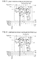
- FIG. 9 is a circuit diagram for explaining the operation of a pixel circuit according to a comparison example in a reset period
- FIG. 10 is a schematic view illustrating the relationship between an electric supply line and the pixel circuit
- FIG. 11 is a circuit diagram illustrating a pixel circuit according to a modification example of the embodiment of the invention.
- FIG. 12 is a circuit diagram illustrating a pixel circuit according to another modification example of the embodiment of the invention.
- FIG. 13 is a perspective view illustrating an overall structure of an electronic apparatus according to the invention.
- FIG. 14 is a perspective view illustrating a detailed structure of the electronic apparatus according to the invention.
- FIG. 15 is a perspective view illustrating the detailed structure of the electronic apparatus according to the invention.
- FIG. 16 is a circuit diagram illustrating a pixel circuit according to a related art.
- FIG. 1 shows a structure of an electro-optical device according to an embodiment of the invention.
- the electro-optical device D is a device included in a variety of electronic apparatuses as a display device.
- the electro-optical device D includes a pixel array portion 10 in which a plurality of pixel circuits P are arranged on a plane, a scan line driving circuit 22 and a data line driving circuit 24 for driving the pixel circuits P, and a voltage generation circuit 27 for generating a variety of voltages used therein.
- the scan line driving circuit 22 , the data line driving circuit 24 and the voltage generation circuit 27 are illustrated in the form of separate circuits, some of or all of the circuits can be formed in the form of an integrated circuit.
- the scan line driving circuit 22 (or the data line driving circuit 24 , or the voltage generation circuit 27 ) can be mounted in the electro-optical device in the form of discrete integrated circuit (IC) chips.
- IC integrated circuit
- the pixel array portion 10 has the number m of control lines 12 extending in an X direction, the number n of data lines 14 extending in an Y direction and perpendicularly intersecting the control lines 12 , and the number m of electric supply lines 17 extending in the Y direction in parallel with the control lines 12 where the numbers m and n are natural numbers.
- Each of the pixel circuits P is disposed at a position corresponding to an intersection out of intersections of the data lines 14 , the control lines and the electric supply lines 17 .
- the pixel circuits P are arranged in the form of a matrix of m rows (vertical direction) and n columns (lateral direction).
- the scan driving circuit 22 selects some pixel circuits out of the plurality of the pixel circuits P row by row in each horizontal scan period.
- the data line driving circuit 24 generate data potentials VD( 1 ) to VD(n) corresponding to the n pixel circuits P associated with a single row selected by the scan driving circuit in each of the horizontal scan periods and transmits them to the corresponding data lines 14 .
- the data potential VD(j) transmitted to a j-th data line 14 is a potential corresponding to a level of gray scale set to the pixel circuit P arranged in a position of in the i-th row and the j-th column.
- the voltage generation circuit 27 generates a potential VEL on the high level side of a power source (hereinafter, referred to as “power source potential”), a potential Gnd on the low level side if the power source (hereinafter, referred to as “ground potential”), and an almost constant potential VST.
- the almost constant potential VST is commonly transmitted to all of the electric supply lines 17 , and then loaded into each of the pixel circuits P.
- FIG. 2 illustrates only one pixel circuit P disposed in a position of the i-th row and the j-th column but the other pixel circuits P have the same structure as the structure shown in FIG. 2 .
- the pixel circuit P has an electro-optical element 11 interposed between a power source line supplied with the power source potential VEL and a ground line supplied with the ground potential Gnd.
- the electro-optical device 11 is a current-driven light-emitting element emitting light with a brightness corresponding to a driving current Iel supplied thereto.
- the electro-optical element 11 is an OLED element having a light-emitting layer made of an organic electro luminance material and interposed between an anode and a cathode.
- the control line 12 illustrated in FIG. 1 is shown as a single line for convenience's sake. However, the control line 12 actually includes four wirings (a scan line 121 , a first control line 123 , a second control line 125 and a light-emitting control line 127 ). Each of the wirings is supplied with a predetermined signal from the scan line driving circuit 22 .
- the i-th scan line 121 is supplied with a scan signal GWRT(i) for selecting the pixel circuits P associated with the i-th row.
- the first control line 123 is supplied with a reset signal GPRE(i) and the second control line 125 is supplied with an initialization signal GINT(i).
- the light-emitting control line 127 is supplied with a light-emitting control signal GEL(i) which defines a period (light emitting period PEL, which will be described below) that it takes for the electro-optical element to actually emit light. Waveforms of these signals and operations of the pixel circuits P corresponding to the waveforms of these signals will be detailed below.
- a drive transistor Tdr which is a p-channel transistor and a light-emitting control transistor Tel are interposed in the middle of a path from the power source line to the electro-optical element 11 .
- the drive transistor Tdr generates a driving current Iel corresponding to a potential VG of a gate thereof.
- a source of the drive transistor Tdr is connected to the power source line and to a drain of the light-emitting control transistor Tel.
- the light-emitting control transistor Tel is an element for defining a period during which the driving current Iel is actually supplied to the electro-optical element 11 .
- a source of the light-emitting control transistor Tel is connected to an anode of the electro-optical element 11 and a gate of the light-emitting control transistor Tel is connected to the light-emitting control line 127 . Accordingly, in a period during which the light-emitting control signal GEL(i) is maintained at a low level, the light emitting control transistor Tel is in the off-state. Thus, the supply of the driving current Iel to the electro-optical element 11 is suspended. On the other hand, when the light emitting control signal GEL(i) is transited to a high level, the light emitting control transistor Tel is turned on and the supply of the driving current Iel to the electro-optical element 11 is resumed.
- the light-emitting control transistor Tel may be interposed between the drive transistor Tdr and the power source line.
- An n-channel transistor Tr 1 is interposed between the gate and the drain of the drive transistor Tdr.
- a gate of the n-channel transistor Tr 1 is connected to the second control line 125 . Accordingly, when the initialization signal GINT(i) is transited to the high level, the transistor Tr 1 is turned on and the drive transistor Tdr is connected as a diode, but when the initialization signal GINT(i) is transited to the low level, the transistor Tr 1 is turned off and the diode connection of the drive transistor Tdr is cancelled.
- a capacitive element C 0 is a capacitor for storing a voltage between a first electrode L 1 and a second electrode L 2 thereof.
- the second electrode L 2 is connected to the gate of the drive transistor Tdr.
- An n-channel transistor Tr 2 is interposed between the first electrode L 1 of the capacitive element C 0 and the data line 14 and a p-channel transistor Tr 3 (a counter conductive transistor to the transistor Tr 2 ) is interposed between the first electrode of the capacitive element C 0 and the electric supply line 17 .
- the transistor Tr 2 is a switching element for performing switching operations in order to control electrical connection and disconnection between the first electrode L 1 and the data line 14 .
- the transistor Tr 3 is a switching element for performing switching operations in order to control electrical connection and disconnection between the first electrode L 1 and the electric supply line 17 .
- the gate of the transistor Tr 2 and the gate of the transistor Tr 3 are commonly connected to the scan line 121 .
- the transistor Tr 2 and the transistor Tr 3 complementarily operate. That is, when the scan signal GWRT(i) has the high level, the transistor Tr 2 is turned on and the transistor Tr 3 is turned off, but when the scan signal GWRT(i) has the low level, the transistor Tr 2 is turned off and the transistor Tr 3 is turned on.
- the n-channel transistor Tr 4 is a switching element interposed between the first electrode L 1 of the capacitive element C 0 and the second electrode L 2 of the capacitive element C 0 in order to control electrical connection and disconnection between the first electrode L 1 and the second electrode L 2 of the capacitive element C 0 .
- an end of the transistor Tr 4 is connected to the first electrode L 1 via the transistor Tr 2 and the other end of the transistor Tr 4 is connected to the second electrode L 2 via the transistor Tr 1 .
- a gate of the transistor Tr 4 is connected to the first control line 123 , In a period during which the transistors Tr 1 and Tr 3 are maintained in the on-state, when the reset signal GPRE(i) is transited to the high level, the transistor Tr 4 is turned on and the first electrode L 1 and the second electrode L 2 are electrically short-circuited.
- FIG. 3 shows the structure of a single pixel of the electro-optical device.
- FIG. 3 illustrates only a semiconductor layer, a gate wiring layer, and a source wiring layer, but the pixel of the electro-optical device includes more layers and elements. For example, these layers are stacked on a glass substrate and insulating layers are interposed between every two layers of the stack thereof. However, in FIG. 3 , the glass substrate and the insulating layers are omitted for convenience's sake.
- an insulating layer is formed on the wiring layer and an electro-optical element 11 connected to the source wiring layer via a terminal T 0 is formed on the insulating layer.
- a ground electrode is formed on the electro-optical element 11 but these are also omitted.
- An insulating layer is provided between the gate wiring layer and the semiconductor layer and thus the capacitive element C 0 is formed by the electrode L 1 provided in the semiconductor layer and the electrode L 2 provided in the gate wiring layer.
- the electric supply line 17 supplied with the power source potential VST is arranged in parallel with the aforementioned control line 12 including four wirings (the scan line 121 , the first control line 123 , the second control line 125 , and the light emitting control line 127 ).
- the electric supply line 17 is formed of a wiring layer (the gate wiring layer) interposed between the scan line 121 and the first control line 123 .
- the electric supply line 17 is connected to sources (or drains) of the transistors Tr 3 and Tr 4 via wirings 17 a of the source wiring layer formed through contact holes.
- scan signals GWRT( 1 ) to GWRT(m) are sequentially transited to the high level in the corresponding horizontal scan periods 1 H, respectively. That is, the scan signal GWRT(i) is maintained at the high level during the i-th horizontal scan period of the vertical scan periods 1 V but maintained at the low level during the other periods.
- the transition of the scan signal GWRT(i) to the high level means the selection of pixel circuits P in the i-th row.
- the period (the horizontal scan period) during which the corresponding scan signal of the scan signals GWRT( 1 ) to GWRT(m) is maintained at the high level is referred to as “writing period PWRT”.
- the electro-optical device may be constructed in a manner such that a rising of the scan signal GWRT(i+1) is started after a falling of the scan signal GWRT(i). That is, there may be an interval between the writing periods PWRT.
- the initialization signal GINT(i) becomes the high level in a period (hereinafter, referred to as “initialization period”) coming right before the writing period starts, that is, right before the scan signal GWRT(i) becomes the high level, but is maintained at the low level during the other periods.
- the initialization period PINT includes a reset period Pa and a compensation period Pb which is subsequent to the reset period Pa.
- a potential VG of the gate of the drive transistor Tdr is set to a potential corresponding to a threshold voltage of the gate of the drive transistor.
- the reset signal GPRE(i) becomes the high level during the reset period within the initialization period PINT in which the initialization signal GINT(i) becomes the high level. However, the reset signal GPRE(i) is maintained at the low level during the other periods.
- the light emission signal GEL(i) becomes the high level in a period PEL (hereinafter, referred to as “light-emitting period”) between the end of the writing period PWRT in which the scan signal GWRT(i) has the high level and the beginning of the initialization period PINT in which the initialization signal GINT(i) has the high level.
- the light emission signal GEL(i) is maintained at the low level during the other periods (the total of the initialization period PINT and the writing period PWRT).
- the operation of the pixel circuit P will be detailed with reference to FIGS. 5 to 8 .
- the operation of the pixel circuit P disposed at a position of the i-th row and the j-th column will be described period by period with respect to the reset period Pa, the compensation period Pb, the writing period PWRT, and the light-emitting period PEL.
- the initialization signal GINT(i) and the reset signal GPRE(i) are maintained at the high level and the scan signal GWRT(i) and the light emission signal GEL(i) are maintained at the low level. Accordingly, as shown in FIG. 5 , the transistors Tr 1 , Tr 3 , and Tr 4 are transited to the on-state but the transistor Tr 2 and the light emitting control transistor Tel are maintained in the off-state. Under this condition, the first electrode L 1 and the second electrode L 2 of the capacitive element C 0 are electrically connected to each other via the transistors Tr 3 , Tr 4 , and Tr 1 .
- the potential VG of the gate of the drive transistor Tdr becomes almost equal to the potential VST generated by the voltage generation circuit 27 .
- the potential VST is lower than a level corresponding to a difference (VEL ⁇ Vth) between the power source potential VEL and the threshold voltage of the drive transistor Tdr.
- the drive transistor Tdr is a p-channel transistor. Accordingly, the drive transistor Tdr is turned on by the supply of the potential VST to the gate. That is, the potential VST is a potential to turn the drive transistor Tdr on when it is supplied.
- the reset signal GPRE(i) is transited to the low level but the other signals are maintained at the same levels as in the reset period Pa.
- the transistor Tr 4 is transited to the off-state from the state shown in FIG. 5 . Accordingly, while the first electrode L 1 connected to the electric supply line 17 via the transistor Tr 3 is maintained at the potential VST, the potential of the second electrode L 2 (that is, the potential VG of the gate of the drive transistor Tdr) is raised to the level corresponding to the difference between the power source potential VEL and the threshold voltage Vth from the potential VST set during the reset period Pa.
- the scan signal GWRT(i) is transited to the high level, and the initialization signal GINT(i), the reset signal GPRE(i), and the lighting signal GEL(i) are maintained at the low level. Accordingly, as shown in FIG. 7 , the transistors Tr 1 , Tr 3 and Tr 4 and the light emitting control transistor Tel are maintained in the off-state, but the transistor Tr 2 is transited to the on-state. As a result, the data line 14 and the first electrode L 1 are electrically connected to each other. Accordingly, the potential of the first electrode L 1 changes to the data potential VD(j) corresponding to a level of gray scale set in the electro-optical element 11 from the potential VST which is supplied during the compensation period Pb.
- the variation in the potential of the second electrode L 2 is determined depending on the capacitance ratio of the capacitance of the capacitive element C 0 to the total of parasitic capacitances (for example, a capacitance attributable to the gate of the drive transistor Tdr and capacitances attributable to a plurality of wirings).
- the capacitance of the capacitive element C 0 is defined as “C”
- the total of the parasitic capacitances is defined as “Cs”
- the variation of the potential of the second electrode L 2 is expressed by the formula “ ⁇ V ⁇ C/(C+Cs)”. Accordingly, the potential VG of the gate of the drive transistor Tdr in the writing period PWRT is stabilized at a level expressed by the following formula (1).
- the transistors Tr 1 and Tr 4 are maintained in the off-state.
- the scan signal GWRT(i) is maintained at the low level during the light-emitting period PEL, as shown in FIG. 8 , the transistor Tr 2 is transited to the off-state and the transistor Tr 3 is transited to the on-state.
- the first electrode L 1 of the capacitive element C 0 is electrically disconnected from the data line 14 thanks to the state of the transistor Tr 2 which is in the off-state, but is electrically connected to the electric supply line 17 via the transistor Tr 3 which is in the on-state.
- the potential of the first electrode L 1 is fixed to the potential VST during the light-emitting period PEL, and thus the potential VG (the potential of the second electrode L 2 ) of the gate of the drive transistor Tdr is maintained at a constant level.
- the capacitive element C 0 serves not only as the coupling capacitor for setting the gate of the drive transistor Tdr to a predetermined potential (the potential expressed by the formula (1)) during the writing period PWRT in which the first electrode L 1 is connected to the data line 14 but also as a storage capacitor for maintaining the gate of the drive transistor Tdr at a constant potential during the light-emitting period PEL in which the first electrode L 1 is connected to the electric supply line 17 .
- the light emitting control transistor Tel is turned on and thus a current path in the driving current Iel is formed. Accordingly, the driving current Iel corresponding to the potential VG of the gate of the drive transistor Tdr is supplied from the power source line to the electro-optical element 11 via the drive transistor Tdr and the light emitting control transistor Tel. Thanks to the supply of the driving current Iel, the electro-optical element 11 emits light with brightness corresponding to the data potential VD(j).
- the electrode L 1 of the capacitive element C 0 becomes the floating state during the light-emitting period and thus the potential of the electrode L 1 easily changes.
- the first electrode L 1 of the capacitive element C 0 is maintained at the potential VST during the light-emitting period PEL, and thus the potential VG of the gate of the drive transistor Tdr is maintained at an almost constant level over the entire light-emitting period PEL. Accordingly, it is possible to make the electro-optical element 11 emit light with a predetermined brightness with high precision by preventing the driving current Iel from varying.
- the capacitance of the capacitive element C 0 can be decreased in comparison with the structure shown in FIG. 15 , in which a large capacitance is needed in order to maintain the potential VG at a constant level.
- the structure shown in FIG. 15 requires an additional storage capacitor C 1 in addition to the capacitive element C 0 in order to securely ensure the potential VG.
- the pixel circuit P is advantageous in that it has a small size because the capacitance needed therefore is decreased.
- the operations of the initialization period PINT (from the reset period Pa to the compensation period Pb), the writing period PWRT, and the light-emitting period PEL with respect to a scan line are repeatedly performed by shifting the scan lines one by one.
- the electro-optical elements 11 in the (i ⁇ 1)-th row performs the operations corresponding to the initialization period PINT (reset period Pa)
- the electro-optical elements 11 in the (i+1)-th row perform the operations corresponding to the light-emitting period PEL. For this reason, as shown in FIG.
- the initialization current of the electro-optical elements 11 in the (i ⁇ 1)-th row flows into the electrical supply line 17 ′ during the electro-optical elements 11 in the (i+1)-th row emit light.
- the potential of the electric supply line 17 ′ changes due to this current.
- the brightness of the light emitted from the electro-optical elements 11 in the (i+1)-th row varys, and thus the flickering occurs.
- the electric supply line 17 is arranged in parallel with the control line 12 including the scan line 121 , the first control line 123 , the second control line 125 , and the light-emitting control line 127 . Accordingly, the states (periods) of the electro-optical elements 11 which can be connected to one electric supply line 17 are identical to another. Accordingly, in the initialization period PINT (reset period Pa), the reset current from, the electro-optical elements 11 in the same row flows along the shared electric supply line 17 , but does not cause any changes in the potentials of the other electric supply lines 17 coupled to electro-optical elements 11 in the other rows. It is therefore possible to prevent occurrence of flickering attributable to the variation in the light-emitting brightness.
- the electric supply lines 17 are arranged to extend in the Y direction perpendicular to the direction of the control line 12 . That is, the number of electric supply lines 17 must be equal to the number of columns of the pixel circuits P. For this reason, according to this embodiment, as shown in FIG. 10B , the electric supply line 17 is arranged to extend in the X direction in parallel with the direction of the control line 12 . Accordingly, a single electric supply line 17 can be shared by every column of the pixel circuits P. In addition, the pixel circuit P is longer in the Y direction than in the X direction. Accordingly, when the electric supply line 17 is arranged in parallel with the control line 12 , an area taken by the electric supply line 17 is relatively small in comparison with an area taken by the electro-optical elements 11 . As a result, an aperture ratio is increased.
- electro-optical devices according to the aforementioned embodiments can be diversely modified. Concrete examples of the modification will be described below. Alternatively, the examples below may be properly combined.
- the transistors Tr 2 and transistor Tr 3 are counter conductive transistors to each other.
- the structure in which the transistor Tr 2 and the transistor Tr 3 operate in a complementary manner is not limited thereto.
- the transistors Tr 2 and Tr 3 may be provided as the same conductive-type transistors (n-channel transistors in this example).
- a gate of the transistor Tr 2 is connected to the first scan line 121 a and a gate of the transistor Tr 3 is connected to the second scan line 121 b .
- the first scan line 121 a is supplied with the first scan signal GWRTa(i) which is the same as the scan signal GWRT(i) shown in FIG.
- the second scan line 121 b is supplied with the second signal GWRTb(i) which is logically reverse to the first scan signal GWRTa(i).
- the operation of this structure is also the same as that in FIGS. 5 to 8 .
- the transistors Tr 2 and Tr 3 can be controlled by the same scan line 121 . Accordingly, such a structure is advantageous in that the structure thereof is simplified.
- FIG. 12 shows a circuit of a pixel circuit P in which the transistor Tr 4 and the light emission control transistor Tel shown in FIG. 2 are omitted.
- the transistor Tr 1 is turned off due to the low level of the initialization signal GINT(i).
- scan signal GWRT(i) is transited to the high level and thus the transistor Tr 2 is turned on.
- the gate of the drive transistor Tdr is set to the potential VG (the formula (1)) corresponding to the data potential VD(i) based on the same principle applied to the first embodiment.
- both of the scan signal GWRT(i) and the initialization signal GINT(i) are maintained at the low level. Thanks to the low level of the scan signal GWRT(i), the transistor Tr 3 is turned on and thus the potential of the first electrode L 1 is fixed at the potential VST. Accordingly, it is possible to prevent the variation in the potential VG of the gate of the drive transistor Tdr from occurring. As described above, since it is possible to avoid the floating state of the first electrode L 1 in the structure shown in FIG. 11 , it is possible to suppress the variation in the potential of the gate of the drive transistor while inhibiting the increase in the size of the pixel circuit P likewise the structure of the first embodiment.
- the conductivity of the transistors constituting the pixel circuit P may be properly changed.
- the drive transistor Tdr shown in FIG. 2 may be provided as an n-channel transistor. Even in this case, the potential VST of the electric supply line 17 is set to a level by which the drive transistor Tdr can be turned on when it is supplied to the gate of the drive transistor Tdr.
- the drive transistor Tdr is a n-channel transistor, the drive transistor Td 1 is interposed between the gate of the drive transistor Tdr and the power source line (potential VEL).
- An OLED element is just an example of the electro-optical element 11 .
- the electro-optical element instead of the OLED element, a variety of light-emitting elements such as an inorganic EL element or an LED (Light Emitting Diode) element may be used as the electro-optical element.
- the electro-optical element is not limited in its structure. That is, the electro-optical element may have any structures as long as it displays a level of gray scale when a current is supplied thereto.
- FIG. 13 shows the structure of a mobile personal computer including the electro-optical device D according to any of the embodiments and modifications thereof as a display device.
- the personal computer 2000 includes the electro-optical device D serving as a display device and a body part 2010 .
- the body part 2010 includes a power switch 2001 and a keyboard 2002 .
- the electro-optical device D includes an OLED element as an electro-optical element 11 , and thus it is possible to display an image at a large view angle, so that it can be conveniently viewed by a viewer.
- FIG. 14 shows the structure of a mobile phone including the electro-optical device D according to any of the embodiments and modifications of the invention therein.
- the mobile phone 3000 includes a plurality of manipulation buttons 3001 , a scroll button 3002 , and the electro-optical device D serving as a display device.
- the scroll button 3002 is manipulated, an image displayed on the electro-optical device D is scrolled.
- FIG. 15 shows the structure of a Personal Digital Assistants (PDA) including the electro-optical device D according to any of the embodiments and modifications of the invention.
- the PDA 4000 includes a plurality of manipulation buttons 4001 , a power switch 4002 , and the electro-optical device D serving as a display device.
- the power switch 4002 is manipulated, a variety of information such as a list of addresses and a time table of schedules is displayed on the electro-optical device D.
- electro-optical devices including electro-optical devices according to any of the embodiments and modifications of the invention.
- Examples thereof are a digital camera, a television, a vide camera, a car navigation device, a pager, an electronic organizer, an electronic paper, a calculator, a word-processor, a workstation, a video phone, a POS terminal, a printer, a scanner, a copying machine, a vide player, a touch panel, and etc.
- the use of the electro-optical device according to the invention is not limited to a display device.
- the electro-optical device according to the invention can be used as the recording head which is a device to expose a photoconductor with a corresponding image to be formed on a recording medium such as paper in an image forming device such as an optical recording printer and an electronic copying machine.
- the electronic circuit in the invention must be broadly understood to include a circuit serving as a unit of exposing in an image forming device as well as a pixel circuit constituting a pixel of a display device.
Abstract
Description
VG=VEL−Vth−k·ΔV (1)
where, k=C/(C+Cs)
(d) Light-Emitting Period PEL
Iel=(β/2)(Vgs−Vth)2=(β/2)(VG−VEL−Vth)2 (2),
The formula (2) is modified to the following formula by the substitution of the formula (1):
Iel=(β/2) {(VEL−Vth−k·ΔV)−VEL−Vth}2=(β/2)(k·ΔV) 2
The driving current Iel supplied to the electro-
Claims (12)
Applications Claiming Priority (4)
| Application Number | Priority Date | Filing Date | Title |
|---|---|---|---|
| JP2006-247656 | 2006-09-13 | ||
| JP2006247656 | 2006-09-13 | ||
| JP2007-128857 | 2007-05-15 | ||
| JP2007128857A JP4259592B2 (en) | 2006-09-13 | 2007-05-15 | Electro-optical device and electronic apparatus |
Publications (2)
| Publication Number | Publication Date |
|---|---|
| US20080074357A1 US20080074357A1 (en) | 2008-03-27 |
| US7928935B2 true US7928935B2 (en) | 2011-04-19 |
Family
ID=39224393
Family Applications (1)
| Application Number | Title | Priority Date | Filing Date |
|---|---|---|---|
| US11/840,490 Active 2029-06-14 US7928935B2 (en) | 2006-09-13 | 2007-08-17 | Electric circuit, driving method thereof, electro-optical device, and electronic apparatus |
Country Status (5)
| Country | Link |
|---|---|
| US (1) | US7928935B2 (en) |
| JP (1) | JP4259592B2 (en) |
| KR (1) | KR101442052B1 (en) |
| CN (1) | CN101145316B (en) |
| TW (1) | TW200818098A (en) |
Cited By (6)
| Publication number | Priority date | Publication date | Assignee | Title |
|---|---|---|---|---|
| US20050219303A1 (en) * | 2003-12-26 | 2005-10-06 | Canon Kabushiki Kaisha | Liquid container and liquid supplying system |
| US20100007647A1 (en) * | 2008-07-09 | 2010-01-14 | Seiko Epson Corporation | Electro-optical device and electronic apparatus |
| US20110001767A1 (en) * | 2009-07-03 | 2011-01-06 | Hitachi Displays, Ltd. | Image display device |
| US8698852B2 (en) | 2010-05-20 | 2014-04-15 | Semiconductor Energy Laboratory Co., Ltd. | Display device and method for driving the same |
| US10657900B2 (en) | 2017-09-22 | 2020-05-19 | Shenzhen China Star Optoelectronics Semiconductor Display Technology Co., Ltd. | Pixel driving circuit, driving method thereof and OLED display panel |
| US20220199013A1 (en) * | 2020-12-22 | 2022-06-23 | Wuhan Tianma Micro-Electronics Co., Ltd. | Display device |
Families Citing this family (16)
| Publication number | Priority date | Publication date | Assignee | Title |
|---|---|---|---|---|
| JP5286992B2 (en) * | 2008-07-09 | 2013-09-11 | セイコーエプソン株式会社 | Electro-optical device and electronic apparatus |
| KR101709749B1 (en) * | 2009-09-16 | 2017-03-08 | 가부시키가이샤 한도오따이 에네루기 켄큐쇼 | Driving method of display device and display device |
| TWI528342B (en) * | 2009-09-16 | 2016-04-01 | 半導體能源研究所股份有限公司 | Display device and driving method thereof |
| KR101760102B1 (en) | 2010-07-19 | 2017-07-21 | 삼성디스플레이 주식회사 | Display, and scan driving apparatus for the display and driving method thereof |
| CN106910464B (en) * | 2011-05-27 | 2020-04-24 | 伊格尼斯创新公司 | System for compensating pixels in a display array and pixel circuit for driving light emitting devices |
| CN103052930A (en) * | 2011-07-27 | 2013-04-17 | 赛普拉斯半导体公司 | Method and apparatus for parallel scanning and data processing for touch sense arrays |
| US9454932B2 (en) * | 2011-11-24 | 2016-09-27 | Joled Inc. | Display device and method of controlling the same |
| US9747834B2 (en) * | 2012-05-11 | 2017-08-29 | Ignis Innovation Inc. | Pixel circuits including feedback capacitors and reset capacitors, and display systems therefore |
| KR101973125B1 (en) * | 2012-12-04 | 2019-08-16 | 엘지디스플레이 주식회사 | Pixel circuit and method for driving thereof, and organic light emitting display device using the same |
| KR102022519B1 (en) * | 2013-05-13 | 2019-09-19 | 삼성디스플레이 주식회사 | Pixel and Organic Light Emitting Display Device Using the same |
| CN103927981B (en) * | 2014-03-24 | 2016-05-18 | 京东方科技集团股份有限公司 | Image element circuit and driving method thereof, display unit |
| KR102635868B1 (en) * | 2016-01-26 | 2024-02-14 | 삼성전자주식회사 | Electronic device and controlling method thereof |
| CN109003579B (en) * | 2018-07-12 | 2020-05-05 | 武汉华星光电半导体显示技术有限公司 | Pixel structure |
| CN111681549B (en) * | 2020-06-16 | 2022-03-18 | 昆山国显光电有限公司 | Array substrate and display panel |
| JP7248181B2 (en) * | 2021-01-07 | 2023-03-29 | セイコーエプソン株式会社 | electro-optical devices and electronic devices |
| CN115101005B (en) * | 2022-07-05 | 2023-07-25 | 深圳市华星光电半导体显示技术有限公司 | Pixel circuit and display panel |
Citations (12)
| Publication number | Priority date | Publication date | Assignee | Title |
|---|---|---|---|---|
| JPH0675246A (en) | 1992-08-28 | 1994-03-18 | Toshiba Corp | Manufacture of active matrix type liquid crystal display element |
| US5917572A (en) | 1995-08-21 | 1999-06-29 | Kabushiki Kaisha Toshiba | Liquid crystal display device comprising switching elements of reverse stagger type and common electrode formed over the entire surface of the substrate including spacers that are constructed of stacked color filter layers |
| US6229506B1 (en) | 1997-04-23 | 2001-05-08 | Sarnoff Corporation | Active matrix light emitting diode pixel structure and concomitant method |
| US20030209990A1 (en) * | 2002-05-08 | 2003-11-13 | Canon Kabushiki Kaisha | EL element drive circuit and display panel |
| JP2004133240A (en) | 2002-10-11 | 2004-04-30 | Sony Corp | Active matrix display device and its driving method |
| JP2004246204A (en) | 2003-02-14 | 2004-09-02 | Sony Corp | Pixel circuit, display device, and driving method of pixel circuit |
| JP2005234593A (en) | 1995-08-21 | 2005-09-02 | Toshiba Electronic Engineering Corp | Liquid crystal display element |
| US20050237283A1 (en) * | 2004-04-22 | 2005-10-27 | Seiko Epson Corporation | Electronic circuit, driving method thereof, electro-optical device, and electronic apparatus |
| US20050237273A1 (en) | 2004-04-22 | 2005-10-27 | Seiko Epson Corporation | Electronic circuit, method of driving electronic circuit, electro-optical device, and electronic apparatus |
| US20060082566A1 (en) | 2004-10-20 | 2006-04-20 | Hajime Akimoto | Image display device |
| JP2006349794A (en) | 2005-06-14 | 2006-12-28 | Seiko Epson Corp | Electronic circuit and its driving method, electrooptical device, and electronic equipment |
| US7456810B2 (en) * | 2001-10-26 | 2008-11-25 | Semiconductor Energy Laboratory Co., Ltd. | Light-emitting device and driving method thereof |
Family Cites Families (2)
| Publication number | Priority date | Publication date | Assignee | Title |
|---|---|---|---|---|
| TW491985B (en) * | 1997-02-17 | 2002-06-21 | Seiko Epson Corporatoin | Display unit |
| TW200540774A (en) * | 2004-04-12 | 2005-12-16 | Sanyo Electric Co | Organic EL pixel circuit |
-
2007
- 2007-05-15 JP JP2007128857A patent/JP4259592B2/en active Active
- 2007-08-17 US US11/840,490 patent/US7928935B2/en active Active
- 2007-08-27 KR KR1020070085984A patent/KR101442052B1/en active IP Right Grant
- 2007-09-12 TW TW096134065A patent/TW200818098A/en unknown
- 2007-09-13 CN CN200710154742XA patent/CN101145316B/en active Active
Patent Citations (15)
| Publication number | Priority date | Publication date | Assignee | Title |
|---|---|---|---|---|
| JPH0675246A (en) | 1992-08-28 | 1994-03-18 | Toshiba Corp | Manufacture of active matrix type liquid crystal display element |
| JP2005234593A (en) | 1995-08-21 | 2005-09-02 | Toshiba Electronic Engineering Corp | Liquid crystal display element |
| US5917572A (en) | 1995-08-21 | 1999-06-29 | Kabushiki Kaisha Toshiba | Liquid crystal display device comprising switching elements of reverse stagger type and common electrode formed over the entire surface of the substrate including spacers that are constructed of stacked color filter layers |
| US6229506B1 (en) | 1997-04-23 | 2001-05-08 | Sarnoff Corporation | Active matrix light emitting diode pixel structure and concomitant method |
| US7456810B2 (en) * | 2001-10-26 | 2008-11-25 | Semiconductor Energy Laboratory Co., Ltd. | Light-emitting device and driving method thereof |
| US20030209990A1 (en) * | 2002-05-08 | 2003-11-13 | Canon Kabushiki Kaisha | EL element drive circuit and display panel |
| US7057588B2 (en) * | 2002-10-11 | 2006-06-06 | Sony Corporation | Active-matrix display device and method of driving the same |
| JP2004133240A (en) | 2002-10-11 | 2004-04-30 | Sony Corp | Active matrix display device and its driving method |
| JP2004246204A (en) | 2003-02-14 | 2004-09-02 | Sony Corp | Pixel circuit, display device, and driving method of pixel circuit |
| US20050237283A1 (en) * | 2004-04-22 | 2005-10-27 | Seiko Epson Corporation | Electronic circuit, driving method thereof, electro-optical device, and electronic apparatus |
| US20050237273A1 (en) | 2004-04-22 | 2005-10-27 | Seiko Epson Corporation | Electronic circuit, method of driving electronic circuit, electro-optical device, and electronic apparatus |
| JP2005309150A (en) | 2004-04-22 | 2005-11-04 | Seiko Epson Corp | Electronic circuit, its driving method, optoelectronic device, and electronic equipment |
| US20060082566A1 (en) | 2004-10-20 | 2006-04-20 | Hajime Akimoto | Image display device |
| JP2006119242A (en) | 2004-10-20 | 2006-05-11 | Hitachi Displays Ltd | Image display apparatus |
| JP2006349794A (en) | 2005-06-14 | 2006-12-28 | Seiko Epson Corp | Electronic circuit and its driving method, electrooptical device, and electronic equipment |
Cited By (19)
| Publication number | Priority date | Publication date | Assignee | Title |
|---|---|---|---|---|
| US8382265B2 (en) * | 2003-12-26 | 2013-02-26 | Canon Kabushiki Kaisha | Liquid container and liquid supplying system |
| US8678569B2 (en) | 2003-12-26 | 2014-03-25 | Canon Kabushiki Kaisha | Liquid container and liquid supplying system |
| US20050219303A1 (en) * | 2003-12-26 | 2005-10-06 | Canon Kabushiki Kaisha | Liquid container and liquid supplying system |
| US20100208015A1 (en) * | 2003-12-26 | 2010-08-19 | Canon Kabushiki Kaisha | Liquid container and liquid supplying system |
| US20100302291A1 (en) * | 2003-12-26 | 2010-12-02 | Canon Kabushiki Kaisha | Liquid container and liquid supplying system |
| US20100309266A1 (en) * | 2003-12-26 | 2010-12-09 | Canon Kabushiki Kaisha | Liquid container and liquid supplying system |
| US20100309265A1 (en) * | 2003-12-26 | 2010-12-09 | Canon Kabushiki Kaisha | Liquid container and liquid supplying system |
| US8454141B2 (en) | 2003-12-26 | 2013-06-04 | Canon Kabushiki Kaisha | Liquid container and liquid supplying system |
| US8801162B2 (en) | 2003-12-26 | 2014-08-12 | Canon Kabushiki Kaisha | Liquid container and liquid supplying system |
| US20080204529A1 (en) * | 2003-12-26 | 2008-08-28 | Canon Kabushiki Kaisha | Liquid container and liquid supplying system |
| US8596770B2 (en) * | 2003-12-26 | 2013-12-03 | Canon Kabushiki Kaisha | Liquid container and liquid supplying system |
| US8529034B2 (en) * | 2003-12-26 | 2013-09-10 | Canon Kabushiki Kaisha | Liquid container and liquid supplying system |
| US8678570B2 (en) * | 2003-12-26 | 2014-03-25 | Canon Kabushiki Kaisha | Liquid container and liquid supplying system |
| US20100007647A1 (en) * | 2008-07-09 | 2010-01-14 | Seiko Epson Corporation | Electro-optical device and electronic apparatus |
| US20110001767A1 (en) * | 2009-07-03 | 2011-01-06 | Hitachi Displays, Ltd. | Image display device |
| US8698852B2 (en) | 2010-05-20 | 2014-04-15 | Semiconductor Energy Laboratory Co., Ltd. | Display device and method for driving the same |
| US10657900B2 (en) | 2017-09-22 | 2020-05-19 | Shenzhen China Star Optoelectronics Semiconductor Display Technology Co., Ltd. | Pixel driving circuit, driving method thereof and OLED display panel |
| US11594178B2 (en) * | 2020-12-22 | 2023-02-28 | Wuhan Tianma Micro-Electronics Co., Ltd. | Display device |
| US20220199013A1 (en) * | 2020-12-22 | 2022-06-23 | Wuhan Tianma Micro-Electronics Co., Ltd. | Display device |
Also Published As
| Publication number | Publication date |
|---|---|
| KR20080024439A (en) | 2008-03-18 |
| JP4259592B2 (en) | 2009-04-30 |
| CN101145316B (en) | 2012-07-18 |
| JP2008096955A (en) | 2008-04-24 |
| CN101145316A (en) | 2008-03-19 |
| US20080074357A1 (en) | 2008-03-27 |
| KR101442052B1 (en) | 2014-09-18 |
| TW200818098A (en) | 2008-04-16 |
Similar Documents
| Publication | Publication Date | Title |
|---|---|---|
| US7928935B2 (en) | Electric circuit, driving method thereof, electro-optical device, and electronic apparatus | |
| US7868854B2 (en) | Electro-optical device and electronic apparatus | |
| KR100724003B1 (en) | Electronic circuit, method of driving electronic circuit, electro-optical device, and electronic apparatus | |
| KR100736740B1 (en) | Electronic device, method of driving the same, electro-optical device, and electronic apparatus | |
| KR101313144B1 (en) | Unit circuit, electro-optical device, and electronic apparatus | |
| TWI457899B (en) | Display device | |
| US8274499B2 (en) | Method for driving pixel circuit, electro-optic device, and electronic apparatus | |
| US7639211B2 (en) | Electronic circuit, electronic device, method of driving electronic device, electro-optical device, and electronic apparatus | |
| JP5360684B2 (en) | Light emitting device, electronic device, and pixel circuit driving method | |
| KR20070120450A (en) | Electronic circuit, method for driving the same, electronic device, and electronic apparatus | |
| JP2010049283A (en) | Electro-optical device and electronic device | |
| JP5392963B2 (en) | Electro-optical device and electronic apparatus | |
| JP5011682B2 (en) | Electronic device and electronic equipment | |
| JP2007025192A (en) | Electronic device, driving method thereof, electro-optical device, and electronic apparatus | |
| JP4946074B2 (en) | Display device, driving method thereof, and electronic apparatus | |
| JP2009222779A (en) | Electro-optical device and electronic apparatus | |
| JP2006349794A (en) | Electronic circuit and its driving method, electrooptical device, and electronic equipment | |
| JP4984520B2 (en) | Electronic circuit, electronic device and electronic equipment | |
| JP5494684B2 (en) | Driving method of electronic circuit | |
| JP2013044986A (en) | Electro-optical device, driving method of electro-optical device and electronic apparatus |
Legal Events
| Date | Code | Title | Description |
|---|---|---|---|
| AS | Assignment |
Owner name: SEIKO EPSON CORPORATION, JAPAN Free format text: ASSIGNMENT OF ASSIGNORS INTEREST;ASSIGNOR:KANDA, EIJI;REEL/FRAME:019719/0261 Effective date: 20070807 |
|
| STCF | Information on status: patent grant |
Free format text: PATENTED CASE |
|
| FEPP | Fee payment procedure |
Free format text: PAYOR NUMBER ASSIGNED (ORIGINAL EVENT CODE: ASPN); ENTITY STATUS OF PATENT OWNER: LARGE ENTITY |
|
| FPAY | Fee payment |
Year of fee payment: 4 |
|
| MAFP | Maintenance fee payment |
Free format text: PAYMENT OF MAINTENANCE FEE, 8TH YEAR, LARGE ENTITY (ORIGINAL EVENT CODE: M1552); ENTITY STATUS OF PATENT OWNER: LARGE ENTITY Year of fee payment: 8 |
|
| AS | Assignment |
Owner name: EL TECHNOLOGY FUSION GODO KAISHA, JAPAN Free format text: ASSIGNMENT OF ASSIGNORS INTEREST;ASSIGNOR:SEIKO EPSON CORPORATION;REEL/FRAME:047998/0879 Effective date: 20181012 |
|
| AS | Assignment |
Owner name: ELEMENT CAPITAL COMMERCIAL COMPANY PTE. LTD., SINGAPORE Free format text: ASSIGNMENT OF ASSIGNORS INTEREST;ASSIGNOR:EL TECHNOLOGY FUSION GODO KAISHA;REEL/FRAME:059435/0428 Effective date: 20211228 |
|
| MAFP | Maintenance fee payment |
Free format text: PAYMENT OF MAINTENANCE FEE, 12TH YEAR, LARGE ENTITY (ORIGINAL EVENT CODE: M1553); ENTITY STATUS OF PATENT OWNER: LARGE ENTITY Year of fee payment: 12 |