US7956429B1 - Insulator layer based MEMS devices - Google Patents
Insulator layer based MEMS devices Download PDFInfo
- Publication number
- US7956429B1 US7956429B1 US12/181,356 US18135608A US7956429B1 US 7956429 B1 US7956429 B1 US 7956429B1 US 18135608 A US18135608 A US 18135608A US 7956429 B1 US7956429 B1 US 7956429B1
- Authority
- US
- United States
- Prior art keywords
- layer
- mems
- actuator
- capacitive plate
- insulator layer
- Prior art date
- Legal status (The legal status is an assumption and is not a legal conclusion. Google has not performed a legal analysis and makes no representation as to the accuracy of the status listed.)
- Active, expires
Links
- 239000012212 insulator Substances 0.000 title claims abstract description 150
- 239000004065 semiconductor Substances 0.000 claims abstract description 77
- 229910052751 metal Inorganic materials 0.000 claims abstract description 25
- 239000002184 metal Substances 0.000 claims abstract description 25
- 238000004519 manufacturing process Methods 0.000 claims abstract description 12
- 238000001465 metallisation Methods 0.000 claims description 91
- 239000003990 capacitor Substances 0.000 claims description 31
- 239000000758 substrate Substances 0.000 claims description 29
- 238000000034 method Methods 0.000 claims description 20
- 239000010410 layer Substances 0.000 description 472
- 229920002120 photoresistant polymer Polymers 0.000 description 62
- 238000005530 etching Methods 0.000 description 23
- 238000000059 patterning Methods 0.000 description 13
- VYPSYNLAJGMNEJ-UHFFFAOYSA-N Silicium dioxide Chemical compound O=[Si]=O VYPSYNLAJGMNEJ-UHFFFAOYSA-N 0.000 description 12
- 239000002356 single layer Substances 0.000 description 10
- 239000004020 conductor Substances 0.000 description 8
- 239000011810 insulating material Substances 0.000 description 8
- 229910052581 Si3N4 Inorganic materials 0.000 description 6
- 230000003044 adaptive effect Effects 0.000 description 6
- 238000001020 plasma etching Methods 0.000 description 6
- 235000012239 silicon dioxide Nutrition 0.000 description 6
- 239000000377 silicon dioxide Substances 0.000 description 6
- HQVNEWCFYHHQES-UHFFFAOYSA-N silicon nitride Chemical compound N12[Si]34N5[Si]62N3[Si]51N64 HQVNEWCFYHHQES-UHFFFAOYSA-N 0.000 description 6
- VYZAMTAEIAYCRO-UHFFFAOYSA-N Chromium Chemical compound [Cr] VYZAMTAEIAYCRO-UHFFFAOYSA-N 0.000 description 4
- RYGMFSIKBFXOCR-UHFFFAOYSA-N Copper Chemical compound [Cu] RYGMFSIKBFXOCR-UHFFFAOYSA-N 0.000 description 4
- RTAQQCXQSZGOHL-UHFFFAOYSA-N Titanium Chemical compound [Ti] RTAQQCXQSZGOHL-UHFFFAOYSA-N 0.000 description 4
- 229910052782 aluminium Inorganic materials 0.000 description 4
- XAGFODPZIPBFFR-UHFFFAOYSA-N aluminium Chemical compound [Al] XAGFODPZIPBFFR-UHFFFAOYSA-N 0.000 description 4
- 229910052804 chromium Inorganic materials 0.000 description 4
- 239000011651 chromium Substances 0.000 description 4
- 229910052802 copper Inorganic materials 0.000 description 4
- 239000010949 copper Substances 0.000 description 4
- PCHJSUWPFVWCPO-UHFFFAOYSA-N gold Chemical compound [Au] PCHJSUWPFVWCPO-UHFFFAOYSA-N 0.000 description 4
- 229910052737 gold Inorganic materials 0.000 description 4
- 239000010931 gold Substances 0.000 description 4
- 238000000623 plasma-assisted chemical vapour deposition Methods 0.000 description 4
- 229910052719 titanium Inorganic materials 0.000 description 4
- 239000010936 titanium Substances 0.000 description 4
- 229910001080 W alloy Inorganic materials 0.000 description 3
- 238000009713 electroplating Methods 0.000 description 3
- 239000000463 material Substances 0.000 description 3
- TWNQGVIAIRXVLR-UHFFFAOYSA-N oxo(oxoalumanyloxy)alumane Chemical compound O=[Al]O[Al]=O TWNQGVIAIRXVLR-UHFFFAOYSA-N 0.000 description 3
- 229910052710 silicon Inorganic materials 0.000 description 3
- 239000010703 silicon Substances 0.000 description 3
- 238000004544 sputter deposition Methods 0.000 description 3
- MAKDTFFYCIMFQP-UHFFFAOYSA-N titanium tungsten Chemical compound [Ti].[W] MAKDTFFYCIMFQP-UHFFFAOYSA-N 0.000 description 3
- 230000005540 biological transmission Effects 0.000 description 2
- 230000008878 coupling Effects 0.000 description 2
- 238000010168 coupling process Methods 0.000 description 2
- 238000005859 coupling reaction Methods 0.000 description 2
- 238000012986 modification Methods 0.000 description 2
- 230000004048 modification Effects 0.000 description 2
- 238000001039 wet etching Methods 0.000 description 2
- 230000008901 benefit Effects 0.000 description 1
- 238000006243 chemical reaction Methods 0.000 description 1
- 238000005516 engineering process Methods 0.000 description 1
- 230000008569 process Effects 0.000 description 1
Images


Classifications
-
- B—PERFORMING OPERATIONS; TRANSPORTING
- B81—MICROSTRUCTURAL TECHNOLOGY
- B81B—MICROSTRUCTURAL DEVICES OR SYSTEMS, e.g. MICROMECHANICAL DEVICES
- B81B7/00—Microstructural systems; Auxiliary parts of microstructural devices or systems
- B81B7/02—Microstructural systems; Auxiliary parts of microstructural devices or systems containing distinct electrical or optical devices of particular relevance for their function, e.g. microelectro-mechanical systems [MEMS]
-
- H—ELECTRICITY
- H01—ELECTRIC ELEMENTS
- H01L—SEMICONDUCTOR DEVICES NOT COVERED BY CLASS H10
- H01L27/00—Devices consisting of a plurality of semiconductor or other solid-state components formed in or on a common substrate
- H01L27/02—Devices consisting of a plurality of semiconductor or other solid-state components formed in or on a common substrate including semiconductor components specially adapted for rectifying, oscillating, amplifying or switching and having at least one potential-jump barrier or surface barrier; including integrated passive circuit elements with at least one potential-jump barrier or surface barrier
- H01L27/04—Devices consisting of a plurality of semiconductor or other solid-state components formed in or on a common substrate including semiconductor components specially adapted for rectifying, oscillating, amplifying or switching and having at least one potential-jump barrier or surface barrier; including integrated passive circuit elements with at least one potential-jump barrier or surface barrier the substrate being a semiconductor body
- H01L27/10—Devices consisting of a plurality of semiconductor or other solid-state components formed in or on a common substrate including semiconductor components specially adapted for rectifying, oscillating, amplifying or switching and having at least one potential-jump barrier or surface barrier; including integrated passive circuit elements with at least one potential-jump barrier or surface barrier the substrate being a semiconductor body including a plurality of individual components in a repetitive configuration
- H01L27/101—Devices consisting of a plurality of semiconductor or other solid-state components formed in or on a common substrate including semiconductor components specially adapted for rectifying, oscillating, amplifying or switching and having at least one potential-jump barrier or surface barrier; including integrated passive circuit elements with at least one potential-jump barrier or surface barrier the substrate being a semiconductor body including a plurality of individual components in a repetitive configuration including resistors or capacitors only
-
- B—PERFORMING OPERATIONS; TRANSPORTING
- B81—MICROSTRUCTURAL TECHNOLOGY
- B81C—PROCESSES OR APPARATUS SPECIALLY ADAPTED FOR THE MANUFACTURE OR TREATMENT OF MICROSTRUCTURAL DEVICES OR SYSTEMS
- B81C1/00—Manufacture or treatment of devices or systems in or on a substrate
- B81C1/00015—Manufacture or treatment of devices or systems in or on a substrate for manufacturing microsystems
- B81C1/00134—Manufacture or treatment of devices or systems in or on a substrate for manufacturing microsystems comprising flexible or deformable structures
- B81C1/0015—Cantilevers
-
- H—ELECTRICITY
- H03—ELECTRONIC CIRCUITRY
- H03H—IMPEDANCE NETWORKS, e.g. RESONANT CIRCUITS; RESONATORS
- H03H3/00—Apparatus or processes specially adapted for the manufacture of impedance networks, resonating circuits, resonators
- H03H3/007—Apparatus or processes specially adapted for the manufacture of impedance networks, resonating circuits, resonators for the manufacture of electromechanical resonators or networks
- H03H3/0072—Apparatus or processes specially adapted for the manufacture of impedance networks, resonating circuits, resonators for the manufacture of electromechanical resonators or networks of microelectro-mechanical resonators or networks
-
- H—ELECTRICITY
- H03—ELECTRONIC CIRCUITRY
- H03H—IMPEDANCE NETWORKS, e.g. RESONANT CIRCUITS; RESONATORS
- H03H9/00—Networks comprising electromechanical or electro-acoustic devices; Electromechanical resonators
- H03H9/02—Details
- H03H9/02244—Details of microelectro-mechanical resonators
- H03H9/02433—Means for compensation or elimination of undesired effects
-
- H—ELECTRICITY
- H03—ELECTRONIC CIRCUITRY
- H03H—IMPEDANCE NETWORKS, e.g. RESONANT CIRCUITS; RESONATORS
- H03H9/00—Networks comprising electromechanical or electro-acoustic devices; Electromechanical resonators
- H03H9/24—Constructional features of resonators of material which is not piezoelectric, electrostrictive, or magnetostrictive
- H03H9/2405—Constructional features of resonators of material which is not piezoelectric, electrostrictive, or magnetostrictive of microelectro-mechanical resonators
Definitions
- Embodiments of the present invention relate to micro-electromechanicalsystems (MEMS) devices integrated into a semiconductor die.
- MEMS devices may be used in tunable or adaptive circuits.
- Tuning and adaptive circuits are two types of circuits commonly used in electronics circuits.
- An example of a tuning circuit is a digitally-controlled oscillator (DCO) used in a frequency synthesizer.
- the DCO may use a resonant circuit having an inductance and a capacitance to establish an oscillator frequency for the DCO.
- the capacitance may be provided by a selectable capacitor bank 10 as illustrated in FIG. 1 , according to the prior art.
- the selectable capacitor bank 10 includes a first capacitive element C 1 , a second capacitive element C 2 , up to and including an Nth capacitive element CN, a first switch 12 , a second switch 14 , up to and including an Nth switch 16 , and control circuitry 18 .
- Each of the capacitive elements C 1 , C 2 , CN is coupled in series with each of the switches 12 , 14 , 16 , respectively, and each capacitive element and switch series coupling is coupled between a first terminal FT and a second terminal ST.
- a control terminal of each of the switches 12 , 14 , 16 is coupled to and controlled by the control circuitry 18 , which receives control information via a control interface CONT.
- the frequency of the DCO is tuned by controlling the capacitance of the selectable capacitor bank 10 , based on the control information, by selecting the appropriate combination of capacitive elements C 1 , C 2 , CN to provide the desired capacitance.
- capacitive elements C 1 , C 2 , CN and switches 12 , 14 , 16 into a common semiconductor die.
- FIG. 2 shows a MEMS switch 20 , according to the prior art.
- the MEMS switch 20 includes a cantilever 22 having a movable contact 24 , a fixed contact 26 electrically coupled to a first terminal 28 , a second terminal 30 electrically coupled to the movable contact 24 , and an actuator 32 electrically coupled to a control terminal 34 .
- the MEMS switch 20 is actuated by applying an actuation signal to the control terminal 34 , the movable and fixed contacts 24 , 26 come together, thereby closing the MEMS switch 20 .
- the MEMS switch 20 When the MEMS switch 20 is closed, the touching movable and fixed contacts 24 , 26 have some contact resistance; therefore, the MEMS switch 20 is called an ohmic MEMS switch.
- the MEMS switch 20 When the MEMS switch 20 is not actuated by removing the actuation signal from the control terminal 34 , the movable and fixed contacts 24 , 26 move apart, thereby opening the MEMS switch 20 .
- the actuator 32 may be formed using a first metal layer (not shown) and the cantilever 22 may be formed using a second metal layer (not shown). Therefore, when the second metal layer is etched to form the cantilever 22 , the metal actuator 32 may be undercut. Thus, there is a need to prevent cantilever 22 to actuator 32 shorting and to prevent metal undercutting of the actuator 32 in a MEMS switch 20 .
- the present invention relates to using an insulator layer between two metal layers of a semiconductor die to provide a micro-electromechanicalsystems (MEMS) device, such as an ohmic MEMS switch or a capacitive MEMS switch.
- MEMS micro-electromechanicalsystems
- the insulator layer may be used to reduce metal undercutting during fabrication, to prevent electrical shorting of a MEMS actuator to a MEMS cantilever, or both.
- the insulator layer may be used as a capacitive dielectric between capacitive plates, which are provided by the two metal layers.
- a fixed capacitive element may be provided by the insulator layer sandwiched between the two metal layers.
- an ohmic MEMS switch, a capacitive MEMS switch, a fixed capacitive element, or any combination thereof may be integrated into a single semiconductor die.
- Combined switching elements and capacitive elements may be used in tunable or adaptive circuits, such as adaptive MEMS driver circuitry, frequency synthesizers, tunable radio frequency (RF) impedance matching circuits, or the like.
- FIG. 1 shows a selectable capacitor bank, according to the prior art.
- FIG. 2 shows a micro-electromechanicalsystems (MEMS) switch, according to the prior art.
- FIG. 3A shows the MEMS switch illustrated in FIG. 2 and FIG. 3B shows a first insulated-actuator MEMS switch, according to one embodiment of the present invention.
- FIG. 4A shows a first MEMS switching capacitive element, according to an alternate embodiment of the present invention.
- FIG. 4B shows an alternate MEMS switching capacitive element, according to another embodiment of the present invention.
- FIG. 4C shows a first integrated fixed capacitive element, according to an additional embodiment of the present invention.
- FIG. 5 shows an integrated selectable capacitor bank, according to one embodiment of the present invention.
- FIG. 6 shows a first region of a semiconductor die, according to one embodiment of the present invention.
- FIG. 7 shows a first patterned photoresist layer added to the semiconductor die illustrated in FIG. 6 .
- FIG. 8 shows a first metallic adhesion layer and a first metallic structural layer added to the semiconductor die illustrated in FIG. 7 .
- FIG. 9 shows the remnants of the first metallic adhesion layer and the first metallic structural layer after lifting-off the portions of the first metallic adhesion layer and the first metallic structural layer that were formed over the first patterned photoresist layer as illustrated in FIG. 8 .
- FIG. 10 shows a second patterned photoresist layer and a first metallization layer added to the semiconductor die illustrated in FIG. 9 .
- FIG. 11 shows the remnants of the first metallization layer after lifting-off the portion of the first metallization layer that was formed over the second patterned photoresist layer as illustrated in FIG. 10 .
- FIG. 12 shows a third insulator layer and a third patterned photoresist layer added to the semiconductor die illustrated in FIG. 11 .
- FIG. 13 shows the remnants of the third insulator layer after etching away a portion of the third insulator layer illustrated in FIG. 12 .
- FIG. 14 shows a first sacrificial layer and a fourth patterned photoresist layer added to the semiconductor die illustrated in FIG. 13 .
- FIG. 15 shows the remnants of the first sacrificial layer after etching away a portion of the first sacrificial layer and shows a second metallization layer added to the semiconductor die illustrated in FIG. 14 .
- FIG. 16 shows a patterned photoresist mold and a MEMS cantilever structure layer added to the semiconductor die illustrated in FIG. 15 .
- FIG. 17 shows the remnants of the second metallization layer and the MEMS cantilever structure layer after etching away a portion of the second metallization layer and the MEMS cantilever structure layer illustrated in FIG. 16 .
- FIG. 18 shows a patterned second sacrificial layer added to the semiconductor die illustrated in FIG. 16 .
- FIG. 19 shows a dome layer added to the semiconductor die illustrated in FIG. 18 to provide the first insulated-actuator MEMS switch.
- FIG. 20 shows a second region of the semiconductor die, according to one embodiment of the present invention.
- FIG. 21 shows the second patterned photoresist layer and the first metallization layer added to the semiconductor die illustrated in FIG. 20 .
- FIG. 22 shows the remnants of the first metallization layer after lifting-off the portion of the first metallization layer that was formed over the second patterned photoresist layer as illustrated in FIG. 21 .
- FIG. 23 shows the third insulator layer and the third patterned photoresist layer added to the semiconductor die illustrated in FIG. 22 .
- FIG. 24 shows the remnants of the third insulator layer after etching away a portion of the third insulator layer illustrated in FIG. 23 .
- FIG. 25 shows the first sacrificial layer and the fourth patterned photoresist layer added to the semiconductor die illustrated in FIG. 24 .
- FIG. 26 shows the remnants of the first sacrificial layer after etching away a portion of the first sacrificial layer and shows the second metallization layer added to the semiconductor die illustrated in FIG. 25 .
- FIG. 27 shows the patterned photoresist mold and the MEMS cantilever structure layer added to the semiconductor die illustrated in FIG. 26 .
- FIG. 28 shows the remnants of the second metallization layer and the MEMS cantilever structure layer after etching away a portion of the second metallization layer and the MEMS cantilever structure layer illustrated in FIG. 27 .
- FIG. 29 shows the second sacrificial layer after patterning and etching added to the semiconductor die illustrated in FIG. 28 .
- FIG. 30 shows the dome layer added to the semiconductor die illustrated in FIG. 29 to provide the first MEMS switching capacitive element.
- FIG. 31 shows a third region of the semiconductor die, according to one embodiment of the present invention.
- FIG. 32 shows the second patterned photoresist layer and the first metallization layer added to the semiconductor die illustrated in FIG. 31 .
- FIG. 33 shows the remnants of the first metallization layer after lifting-off the portion of the first metallization layer that was formed over the second patterned photoresist layer as illustrated in FIG. 32 .
- FIG. 34 shows the third insulator layer and the third patterned photoresist layer added to the semiconductor die illustrated in FIG. 33 .
- FIG. 35 shows the remnants of the third insulator layer after etching away a portion of the third insulator layer illustrated in FIG. 34 .
- FIG. 36 shows the patterned photoresist mold and the MEMS cantilever structure layer added to the semiconductor die illustrated in FIG. 35 .
- FIG. 37 shows the remnants of the second metallization layer and the MEMS cantilever structure layer after etching away a portion of the second metallization layer and the MEMS cantilever structure layer illustrated in FIG. 36 to provide the first integrated fixed capacitive element.
- FIG. 38 shows an application example of the present invention used in a mobile terminal.
- the present invention relates to using an insulator layer between two metal layers of a semiconductor die to provide a micro-electromechanicalsystems (MEMS) device, such as an ohmic MEMS switch or a capacitive MEMS switch.
- MEMS micro-electromechanicalsystems
- the insulator layer may be used to reduce metal undercutting during fabrication, to prevent electrical shorting of a MEMS actuator to a MEMS cantilever, or both.
- the insulator layer may be used as a capacitive dielectric between capacitive plates, which are provided by the two metal layers.
- a fixed capacitive element may be provided by the insulator layer between the two metal layers.
- an ohmic MEMS switch, a capacitive MEMS switch, a fixed capacitive element, or any combination thereof may be integrated into a single semiconductor die.
- Combined switching elements and capacitive elements may be used in tunable or adaptive circuits, such as adaptive MEMS driver circuitry, frequency synthesizers, tunable radio frequency (RF) impedance matching circuits, or the like.
- FIG. 3A shows the MEMS switch 20 illustrated in FIG. 2 and FIG. 3B shows a first insulated-actuator MEMS switch 36 , according to one embodiment of the present invention.
- the first insulated-actuator MEMS switch 36 is an ohmic MEMS switch similar to the MEMS switch 20 illustrated in FIG. 3A .
- the first insulated-actuator MEMS switch 36 includes an actuator insulator 38 over the actuator 32 .
- the actuator insulator 38 may prevent shorting of the cantilever 22 to the actuator 32 when the first insulated-actuator MEMS switch 36 is actuated, may reduce or prevent metal undercutting of the actuator 32 during fabrication, or both.
- FIG. 4A shows a first MEMS switching capacitive element 40 , according to an alternate embodiment of the present invention.
- the first MEMS switching capacitive element 40 includes a cantilever 42 , which functions as a movable capacitive plate, a first terminal 44 electrically coupled to a fixed capacitive plate 46 , a second terminal 48 electrically coupled to the cantilever 42 , an actuator 50 electrically coupled to a control terminal 52 , and a capacitive dielectric 54 .
- the movable capacitive plate, the capacitive dielectric 54 , and the fixed capacitive plate 46 form a selectable capacitive element.
- the first MEMS switching capacitive element 40 When no actuation signal is applied to the control terminal 52 , the first MEMS switching capacitive element 40 is not actuated. Therefore, non-actuated spacing between the movable capacitive plate and the fixed capacitive plate 46 establishes a first capacitance presented to the first and second terminals 44 , 48 . However, when an actuation signal is applied to the control terminal 52 , the first MEMS switching capacitive element 40 is actuated, thereby moving the cantilever 42 closer to the fixed capacitive plate 46 . Therefore, actuated spacing between the movable capacitive plate and the fixed capacitive plate 46 establishes a second capacitance presented to the first and second terminals 44 , 48 . The second capacitance is greater than the first capacitance due to the reduced spacing between the movable capacitive plate and the fixed capacitive plate 46 .
- the capacitive dielectric 54 insulates the cantilever 42 from the fixed capacitive plate 46 .
- the capacitive dielectric 54 may prevent shorting of the cantilever 42 to the actuator 50 when the first MEMS switching capacitive element 40 is actuated, may reduce or prevent metal undercutting of the actuator 50 during fabrication, or both.
- FIG. 4B shows an alternate MEMS switching capacitive element 56 , according to another embodiment of the present invention.
- the alternate MEMS switching capacitive element 56 includes the cantilever 42 , which functions as a movable capacitive plate, the first terminal 44 electrically coupled to a combined actuator and fixed capacitive plate 57 , the second terminal 48 electrically coupled to the cantilever 42 , and the capacitive dielectric 54 .
- the movable capacitive plate, the capacitive dielectric 54 , and the combined actuator and fixed capacitive plate 57 form a selectable capacitive element.
- the alternate MEMS switching capacitive element 56 When no actuation signal is applied to the first terminal 44 , the alternate MEMS switching capacitive element 56 is not actuated. Therefore, non-actuated spacing between the movable capacitive plate and the combined actuator and fixed capacitive plate 57 establishes a first capacitance presented to the first and second terminals 44 , 48 . However, when an actuation signal is applied to the first terminal 44 , the alternate MEMS switching capacitive element 56 is actuated, thereby moving the cantilever 42 closer to the combined actuator and fixed capacitive plate 57 . Therefore, actuated spacing between the movable capacitive plate and the combined actuator and fixed capacitive plate 57 establishes a second capacitance presented to the first and second terminals 44 , 48 . The second capacitance is greater than the first capacitance due to the reduced spacing between the movable capacitive plate and the combined actuator and fixed capacitive plate 57 .
- the capacitive dielectric 54 insulates the cantilever 42 from the combined actuator and fixed capacitive plate 57 .
- the capacitive dielectric 54 may prevent shorting of the cantilever 42 to the combined actuator and fixed capacitive plate 57 when the alternate MEMS switching capacitive element 56 is actuated, may reduce or prevent metal undercutting of the combined actuator and fixed capacitive plate 57 during fabrication, or both.
- a control terminal 52 in addition to the first terminal 44 , may be electrically coupled to the combined actuator and fixed capacitive plate 57 .
- FIG. 4C shows a first integrated fixed capacitive element 58 , according to an additional embodiment of the present invention.
- the first integrated fixed capacitive element 58 includes a first capacitive plate 59 electrically coupled to a first terminal 60 , a second capacitive plate 62 electrically coupled to a second terminal 64 , and a fixed dielectric 66 , which is between the first and second capacitive plates 59 , 62 .
- the first and second capacitive plates 59 , 62 and the fixed dielectric 66 form a capacitive element with a capacitance presented to the first and second terminals 60 , 64 .
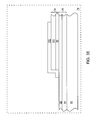
- FIG. 5 shows an integrated selectable capacitor bank 68 , according to one embodiment of the present invention.
- the integrated selectable capacitor bank 68 includes the first integrated fixed capacitive element 58 , a second integrated fixed capacitive element 70 , the first insulated-actuator MEMS switch 36 , a second insulated-actuator MEMS switch 72 , the first MEMS switching capacitive element 40 , a second MEMS switching capacitive element 74 , and control circuitry 76 .
- Each of the integrated fixed capacitive elements 58 , 70 is coupled in series with each of the insulated-actuator MEMS switches 36 , 72 , respectively, and each capacitive element and switch series coupling is coupled between a first terminal FT and a second terminal ST.
- each of the MEMS switching capacitive elements 40 , 74 is coupled between the first terminal FT and the second terminal ST.
- a control terminal of each of the insulated-actuator MEMS switches 36 , 72 and each of the MEMS switching capacitive elements 40 , 74 is coupled to and controlled by the control circuitry 76 , which receives control information via a control interface CONT.
- the capacitance of the integrated selectable capacitor bank 68 is presented to the first and second terminals FT, ST.
- An external device (not shown) controls the capacitance of the integrated selectable capacitor bank 68 based on the control information by selecting the appropriate combination of integrated fixed capacitive elements 58 , 70 and selected MEMS switching capacitive elements 40 , 74 to provide the desired capacitance.
- any or all of the first integrated fixed capacitive element 58 , the second integrated fixed capacitive element 70 , the first insulated-actuator MEMS switch 36 , the second insulated-actuator MEMS switch 72 , the first MEMS switching capacitive element 40 , and the second MEMS switching capacitive element 74 may be omitted. Further, additional insulated-actuator MEMS switches 36 , 72 , MEMS switching capacitive elements 40 , 74 , integrated fixed capacitive elements 58 , 70 , or any combination thereof, may be included.
- FIG. 6 shows a first region of a semiconductor die 78 , according to one embodiment of the present invention.
- the semiconductor die 78 includes a substrate 80 , which may be a semiconductor substrate, such as Silicon.
- a substrate insulator layer 82 is over the substrate 80 and includes a first insulator layer 84 and a second insulator layer 86 .
- the first insulator layer 84 may include Silicon Nitride and the second insulator layer 86 may include Silicon Dioxide.
- the substrate insulator layer 82 may be a single layer, may include multiple layers, the first insulator layer 84 may include other insulating material, the second insulator layer 86 may include other insulating material, or any combination thereof.
- FIG. 7 shows a first patterned photoresist layer 88 added to the semiconductor die 78 illustrated in FIG. 6 and formed over the second insulator layer 86 .
- FIG. 8 shows a first metallic adhesion layer 90 and a first metallic structural layer 92 added to the semiconductor die 78 illustrated in FIG. 7 .
- the first metallic adhesion layer 90 is formed over the first patterned photoresist layer 88 and the second insulator layer 86 .
- the first metallic structural layer 92 is formed over the first metallic adhesion layer 90 , which may include Titanium, Chromium, Titanium Tungsten alloy, or other suitable material, and is used to bond the first metallic structural layer 92 to the substrate insulator layer 82 .
- the first metallic structural layer 92 may include Gold, Copper, or Aluminum.
- FIG. 9 shows the remnants of the first metallic adhesion layer 90 and the first metallic structural layer 92 after lifting-off the portion of the first metallic adhesion layer 90 and the first metallic structural layer 92 that were formed over the first patterned photoresist layer 88 as illustrated in FIG. 8 .
- the remnants of the first metallic adhesion layer 90 and the first metallic structural layer 92 provide a bump, which will be used to form the fixed contact 26 of the first insulated-actuator MEMS switch 36 .
- Alternate embodiments of the present invention may use other techniques to form the bump, such as using a single layer to form the bump, using other methods of patterning the first metallic adhesion layer 90 and the first metallic structural layer 92 , or the like.
- FIG. 10 shows a second patterned photoresist layer 94 and a first metallization layer 96 added to the semiconductor die 78 illustrated in FIG. 9 .
- the first metallization layer 96 includes a second metallic adhesion layer 98 and a second metallic structural layer 100 .
- the second patterned photoresist layer 94 is formed over the second insulator layer 86 .
- the second metallic adhesion layer 98 is formed over the second patterned photoresist layer 94 , the second insulator layer 86 , and the first metallic structural layer 92 .
- the second metallic structural layer 100 is formed over the second metallic adhesion layer 98 .
- the second metallic adhesion layer 98 may include Titanium, Chromium, Titanium Tungsten alloy, or other suitable material, and is used to bond the second metallic structural layer 100 to the substrate insulator layer 82 , to the first metallic structural layer 92 , or both.
- the second metallic structural layer 100 may include Gold, Copper, or Aluminum.
- the first metallization layer 96 may be a single layer, may include multiple layers, the second metallic adhesion layer 98 may include other conductive material, the second metallic structural layer 100 may include other conductive material, or any combination thereof.
- FIG. 11 shows the remnants of the first metallization layer 96 after lifting-off the portion of the first metallization layer 96 that was formed over the second patterned photoresist layer 94 as illustrated in FIG. 10 .
- Alternate embodiments of the present invention may use other techniques to pattern the first metallization layer 96 , such as using a single layer to provide the first metallization layer 96 , using other methods of patterning the second metallic adhesion layer 98 , using other methods of patterning the second metallic structural layer 100 , or the like.
- FIG. 12 shows a third insulator layer 102 and a third patterned photoresist layer 104 added to the semiconductor die 78 illustrated in FIG. 11 .
- the third insulator layer 102 is formed over the second metallic structural layer 100 and the second insulator layer 86 .
- the third insulator layer 102 is deposited over the second metallic structural layer 100 using plasma enhanced chemical vapor deposition (PECVD).
- PECVD plasma enhanced chemical vapor deposition
- the third insulator layer 102 is deposited over the second metallic structural layer 100 by sputtering.
- the third patterned photoresist layer 104 is formed over the third insulator layer 102 .
- the third insulator layer 102 may include Silicon Nitride, Silicon Dioxide, or Aluminum Oxide.
- FIG. 13 shows the remnants of the third insulator layer 102 after etching away a portion of the third insulator layer 102 illustrated in FIG. 12 , and after removing the third patterned photoresist layer 104 after etching. Alternate embodiments of the present invention may use other ways of patterning the third insulator layer 102 .
- RIE reactive ion etching
- FIG. 14 shows a first sacrificial layer 106 and a fourth patterned photoresist layer 108 added to the semiconductor die 78 illustrated in FIG. 13 .
- the first sacrificial layer 106 is formed over the third insulator layer 102 and the second metallic structural layer 100 .
- the fourth patterned photoresist layer 108 is formed over the first sacrificial layer 106 .
- the first sacrificial layer 106 will be used to provide clearance between the movable contact 24 and the fixed contact 26 of the first insulated-actuator MEMS switch 36 . Areas of the first sacrificial layer 106 not covered by the fourth patterned photoresist layer 108 are etched away.
- the first sacrificial layer 106 is etched using RIE.
- the first sacrificial layer 106 is etched using wet etching.
- FIG. 15 shows the remnants of the first sacrificial layer 106 after etching away a portion of the first sacrificial layer 106 and after removing the fourth patterned photoresist layer 108 after etching, and shows a second metallization layer 110 added to the semiconductor die 78 illustrated in FIG. 14 .
- the second metallization layer 110 includes a third metallic adhesion layer 112 and a third metallic structural layer 114 .
- the third metallic adhesion layer 112 is formed over the third insulator layer 102 , the second metallic structural layer 100 , and the first sacrificial layer 106 .
- the third metallic structural layer 114 is formed over the third metallic adhesion layer 112 .
- Alternate embodiments of the present invention may use other ways of patterning the first sacrificial layer 106 .
- FIG. 16 shows a patterned photoresist mold 116 and a MEMS cantilever structure layer 118 added to the semiconductor die 78 illustrated in FIG. 15 .
- the patterned photoresist mold 116 is formed over the third metallic structural layer 114 .
- the MEMS cantilever structure layer 118 is then formed over the portion of the third metallic structural layer 114 that is not covered by the patterned photoresist mold 116 .
- the MEMS cantilever structure layer 118 may formed over the third metallic structural layer 114 by electroplating or by another technique.
- the second metallization layer 110 may function as a seed layer for the MEMS cantilever structure layer 118 .
- the patterned photoresist mold 116 is removed.
- FIG. 17 shows the remnants of the second metallization layer 110 and the MEMS cantilever structure layer 118 after etching away a portion of the second metallization layer 110 and the MEMS cantilever structure layer 118 illustrated in FIG. 16 .
- the third insulator layer 102 protects the first metallization layer 96 from being undercut as a result of etching the second metallization layer 110 .
- FIG. 18 shows a patterned second sacrificial layer 120 added to the semiconductor die 78 illustrated in FIG. 17 .
- the patterned second sacrificial layer 120 is formed over the MEMS cantilever structure layer 118 , the third metallic structural layer 114 , the third metallic adhesion layer 112 , the first sacrificial layer 106 , the third insulator layer 102 , and the second metallic structural layer 100 .
- FIG. 19 shows a dome layer 122 added to the semiconductor die 78 illustrated in FIG. 18 to provide the first insulated-actuator MEMS switch 36 .
- the dome layer 122 is formed over the patterned second sacrificial layer 120 to provide a dome for the first insulated-actuator MEMS switch 36 .
- the first sacrificial layer 106 and the patterned second sacrificial layer 120 were evacuated to provide space for the first insulated-actuator MEMS switch 36 to operate freely.
- the first sacrificial layer 106 and the patterned second sacrificial layer 120 may have been evacuated through evacuation passages, holes, or both in the dome layer 122 , in the third insulator layer 102 , in the first metallization layer 96 , or any combination thereof.
- the dome layer 122 may include insulating material or conducting material. In one embodiment of the present invention, the dome layer 122 is conducting and the third insulator layer 102 electrically insulates the dome layer 122 from the first metallization
- the MEMS cantilever structure layer 118 , the third metallic structural layer 114 , and the third metallic adhesion layer 112 provide the cantilever 22 .
- the second metallic structural layer 100 provides the fixed contact 26
- the third metallic adhesion layer 112 provides the movable contact 24 .
- the first metallization layer 96 provides the actuator 32 and the third insulator layer 102 provides the actuator insulator 38 .
- the fixed contact 26 is electrically coupled to the first terminal 28 ( FIG. 3A ) through the second metallic structural layer 100
- the second terminal 30 ( FIG. 3A ) is electrically coupled to the movable contact 24 through the third metallic adhesion layer 112
- the actuator 32 is electrically coupled to the control terminal 34 ( FIG. 3A ) through the first metallization layer 96 .
- a non-cantilever architecture may be used, a different movable member instead of the cantilever 22 may be used, the fixed contact 26 , the movable contact 24 , the actuator 32 , the actuator insulator 38 , the cantilever 22 , or any combination thereof may be provided using a different architecture. Additional layers may be included in any order.
- any of the first insulator layer 84 , the second insulator layer 86 , the first metallic adhesion layer 90 , the first metallic structural layer 92 , the second metallic adhesion layer 98 , the second metallic structural layer 100 , the third metallic adhesion layer 112 , the third metallic structural layer 114 , the MEMS cantilever structure layer 118 , and the dome layer 122 may be omitted.
- FIG. 20 shows a second region of the semiconductor die 78 , according to one embodiment of the present invention.
- the semiconductor die 78 includes the substrate 80 , which may be a semiconductor substrate, such as Silicon.
- the substrate insulator layer 82 is over the substrate 80 and includes the first insulator layer 84 and the second insulator layer 86 .
- the first insulator layer 84 may include Silicon Nitride and the second insulator layer 86 may include Silicon Dioxide.
- the substrate insulator layer 82 may be a single layer, may include multiple layers, the first insulator layer 84 may include other insulating material, the second insulator layer 86 may include other insulating material, or any combination thereof.
- FIG. 21 shows the second patterned photoresist layer 94 and the first metallization layer 96 added to the semiconductor die 78 illustrated in FIG. 20 .
- the first metallization layer 96 includes the second metallic adhesion layer 98 and the second metallic structural layer 100 .
- the second patterned photoresist layer 94 is formed over the second insulator layer 86 .
- the second metallic adhesion layer 98 is formed over the second patterned photoresist layer 94 and the second insulator layer 86 .
- the second metallic structural layer 100 is formed over the second metallic adhesion layer 98 .
- the second metallic adhesion layer 98 may include Titanium or Chromium and is used to bond the second metallic structural layer 100 to the substrate insulator layer 82 .
- the second metallic structural layer 100 may include Gold, Copper, or Aluminum.
- the first metallization layer 96 may be a single layer, may include multiple layers, the second metallic adhesion layer 98 may include other conductive material, the second metallic structural layer 100 may include other conductive material, or any combination thereof.
- FIG. 22 shows the remnants of the first metallization layer 96 after lifting-off the portion of the first metallization layer 96 that was formed over the second patterned photoresist layer 94 as illustrated in FIG. 21 .
- Alternate embodiments of the present invention may use other techniques to pattern the first metallization layer 96 , such as using a single layer to provide the first metallization layer 96 , using other methods of patterning the second metallic adhesion layer 98 , using other methods of patterning the second metallic structural layer 100 , or the like.
- FIG. 23 shows the third insulator layer 102 and the third patterned photoresist layer 104 added to the semiconductor die 78 illustrated in FIG. 22 .
- the third insulator layer 102 is formed over the second metallic structural layer 100 and the second insulator layer 86 .
- the third insulator layer 102 is deposited over the second metallic structural layer 100 using PECVD.
- the third insulator layer 102 is deposited over the second metallic structural layer 100 by sputtering.
- the third patterned photoresist layer 104 is formed over the third insulator layer 102 .
- the third insulator layer 102 may include Silicon Nitride, Silicon Dioxide, or Aluminum Oxide.
- FIG. 24 shows the remnants of the third insulator layer 102 after etching away a portion of the third insulator layer 102 illustrated in FIG. 23 , and after removing the third patterned photoresist layer 104 after etching. Alternate embodiments of the present invention may use other ways of patterning the third insulator layer 102 .
- FIG. 25 shows the first sacrificial layer 106 and the fourth patterned photoresist layer 108 added to the semiconductor die 78 illustrated in FIG. 24 .
- the first sacrificial layer 106 is formed over the third insulator layer 102 and the second metallic structural layer 100 .
- the fourth patterned photoresist layer 108 is formed over the first sacrificial layer 106 .
- the first sacrificial layer 106 will be used to provide clearance between the cantilever 42 , which functions as the movable capacitive plate, and the capacitive dielectric 54 of the alternate MEMS switching capacitive element 56 . Areas of the first sacrificial layer 106 not covered by the fourth patterned photoresist layer 108 are etched away.
- the first sacrificial layer 106 is etched using RIE.
- the first sacrificial layer 106 is etched using wet etching.
- FIG. 26 shows the remnants of the first sacrificial layer 106 after etching away a portion of the first sacrificial layer 106 and shows the second metallization layer 110 added to the semiconductor die 78 illustrated in FIG. 25 .
- the second metallization layer 110 includes the third metallic adhesion layer 112 and the third metallic structural layer 114 .
- the third metallic adhesion layer 112 is formed over the third insulator layer 102 , the second metallic structural layer 100 , and the first sacrificial layer 106 .
- the third metallic structural layer 114 is formed over the third metallic adhesion layer 112 .
- Alternate embodiments of the present invention may use other ways of patterning the first sacrificial layer 106 .
- FIG. 27 shows the patterned photoresist mold 116 and the MEMS cantilever structure layer 118 added to the semiconductor die 78 illustrated in FIG. 26 .
- the patterned photoresist mold 116 is formed over the third metallic structural layer 114 .
- the MEMS cantilever structure layer 118 is then formed over the portion of the third metallic structural layer 114 that is not covered by the patterned photoresist mold 116 .
- the MEMS cantilever structure layer 118 may be formed over the third metallic structural layer 114 by electroplating or by another technique.
- the second metallization layer 110 may function as a seed layer for the MEMS cantilever structure layer 118 .
- the patterned photoresist mold 116 is removed.
- FIG. 28 shows the remnants of the second metallization layer 110 and the MEMS cantilever structure layer 118 after etching away a portion of the second metallization layer 110 and the MEMS cantilever structure layer 118 illustrated in FIG. 27 .
- the third insulator layer 102 protects the first metallization layer 96 from being undercut as a result of etching the second metallization layer 110 .
- FIG. 29 shows the patterned second sacrificial layer 120 added to the semiconductor die 78 illustrated in FIG. 28 .
- the patterned second sacrificial layer 120 is formed over the MEMS cantilever structure layer 118 , the third metallic structural layer 114 , the third metallic adhesion layer 112 , the first sacrificial layer 106 , the third insulator layer 102 , and the second metallic structural layer 100 .
- FIG. 30 shows the dome layer 122 added to the semiconductor die 78 illustrated in FIG. 29 to provide the alternate MEMS switching capacitive element 56 .
- the dome layer 122 is formed over the patterned second sacrificial layer 120 to provide a dome for the alternate MEMS switching capacitive element 56 .
- the first sacrificial layer 106 and the patterned second sacrificial layer 120 were evacuated to provide space for the alternate MEMS switching capacitive element 56 to operate freely.
- the first sacrificial layer 106 and the patterned second sacrificial layer 120 may have been evacuated through evacuation passages, holes, or both in the dome layer 122 , in the third insulator layer 102 , in the first metallization layer 96 , or any combination thereof.
- the dome layer 122 may include insulating material or conducting material. In one embodiment of the present invention, the dome layer 122 is conducting and the third insulator layer 102 electrically insulates the dome layer 122 from the first metallization layer 96
- the MEMS cantilever structure layer 118 , the third metallic structural layer 114 , and the third metallic adhesion layer 112 provide the cantilever 42 , which functions as the movable capacitive plate.
- the first metallization layer 96 provides the combined actuator and fixed capacitive plate 57 and the third insulator layer 102 provides the capacitive dielectric 54 .
- the first terminal 44 ( FIG. 4B ) is electrically coupled to the combined actuator and fixed capacitive plate 57 through the first metallization layer 96 .
- the second terminal 48 ( FIG. 4B ) is electrically coupled to the cantilever 42 through the second metallization layer 110 .
- a non-cantilever architecture may be used, a different movable member instead of the cantilever 42 may be used, the movable capacitive plate, the combined actuator and fixed capacitive plate 57 , the capacitive dielectric 54 , or any combination thereof may be provided using a different architecture. Additional layers may be included in any order.
- any of the first insulator layer 84 , the second insulator layer 86 , the first metallic adhesion layer 90 , the first metallic structural layer 92 , the second metallic adhesion layer 98 , the second metallic structural layer 100 , the third metallic adhesion layer 112 , the third metallic structural layer 114 , the MEMS cantilever structure layer 118 , and the dome layer 122 may be omitted.
- the semiconductor die 78 may provide the first MEMS switching capacitive element 40 by separating the combined actuator and fixed capacitive plate 57 illustrated in FIG. 30 into a separate actuator 50 and fixed capacitive plate 46 .
- FIG. 31 shows a third region of the semiconductor die 78 , according to one embodiment of the present invention.
- the semiconductor die 78 includes the substrate 80 , which may be a semiconductor substrate, such as Silicon.
- the substrate insulator layer 82 is over the substrate 80 and includes the first insulator layer 84 and the second insulator layer 86 .
- the first insulator layer 84 may include Silicon Nitride and the second insulator layer 86 may include Silicon Dioxide.
- the substrate insulator layer 82 may be a single layer, may include multiple layers, the first insulator layer 84 may include other insulating material, the second insulator layer 86 may include other insulating material, or any combination thereof.
- FIG. 32 shows the second patterned photoresist layer 94 and the first metallization layer 96 added to the semiconductor die 78 illustrated in FIG. 31 .
- the first metallization layer 96 includes the second metallic adhesion layer 98 and the second metallic structural layer 100 .
- the second patterned photoresist layer 94 is formed over the second insulator layer 86 .
- the second metallic adhesion layer 98 is formed over the second patterned photoresist layer 94 and the second insulator layer 86 .
- the second metallic structural layer 100 is formed over the second metallic adhesion layer 98 .
- the second metallic adhesion layer 98 may include Titanium, Chromium, Titanium Tungsten alloy, or other suitable material, and is used to bond the second metallic structural layer 100 to the substrate insulator layer 82 .
- the second metallic structural layer 100 may include Gold, Copper, or Aluminum.
- the first metallization layer 96 may be a single layer, may include multiple layers, the second metallic adhesion layer 98 may include other conductive material, the second metallic structural layer 100 may include other conductive material, or any combination thereof.
- FIG. 33 shows the remnants of the first metallization layer 96 after lifting-off the portion of the first metallization layer 96 that was formed over the second patterned photoresist layer 94 as illustrated in FIG. 32 .
- Alternate embodiments of the present invention may use other techniques to pattern the first metallization layer 96 , such as using a single layer to provide the first metallization layer 96 , using other methods of patterning the second metallic adhesion layer 98 , using other methods of patterning the second metallic structural layer 100 , or the like.
- FIG. 34 shows the third insulator layer 102 and the third patterned photoresist layer 104 added to the semiconductor die 78 illustrated in FIG. 33 .
- the third insulator layer 102 is formed over the second metallic structural layer 100 and the second insulator layer 86 .
- the third insulator layer 102 is deposited over the second metallic structural layer 100 using PECVD.
- the third insulator layer 102 is deposited over the second metallic structural layer 100 by sputtering.
- the third patterned photoresist layer 104 is formed over the third insulator layer 102 .
- the third insulator layer 102 may include Silicon Nitride, Silicon Dioxide, or Aluminum Oxide.
- FIG. 35 shows the remnants of the third insulator layer 102 after etching away a portion of the third insulator layer 102 illustrated in FIG. 34 , and after removing the third patterned photoresist layer 104 after etching. Alternate embodiments of the present invention may use other ways of patterning the third insulator layer 102 .
- the MEMS cantilever structure layer 118 is then formed over the portion of the third metallic structural layer 114 that is not covered by the patterned photoresist mold 116 .
- the MEMS cantilever structure layer 118 may be formed over the third metallic structural layer 114 by electroplating or by another technique.
- the second metallization layer 110 may function as a seed layer for the MEMS cantilever structure layer 118 .
- the patterned photoresist mold 116 is removed.
- FIG. 37 shows the remnants of the second metallization layer 110 and the MEMS cantilever structure layer 118 after etching away a portion of the second metallization layer 110 and the MEMS cantilever structure layer 118 illustrated in FIG. 36 to provide the first integrated fixed capacitive element 58 .
- the MEMS cantilever structure layer 118 , the third metallic structural layer 114 , and the third metallic adhesion layer 112 provide the first capacitive plate 59 .
- the first metallization layer 96 provides the second capacitive plate 62
- the third insulator layer 102 provides the fixed dielectric 66 , which is between the first and second capacitive plates 59 , 62 .
- the first capacitive plate 59 is electrically coupled to the first terminal 60 ( FIG. 4C ) through the first metallization layer 96
- the second capacitive plate 62 is electrically coupled to the second terminal 64 ( FIG. 4C ) through the second metallization layer 110 .
- first integrated fixed capacitive element 58 the first capacitive plate 59 , the first terminal 60 , the second capacitive plate 62 , the second terminal 64 , the fixed dielectric 66 , or any combination thereof may be provided using a different architecture. Additional layers may be included in any order. Any of the first insulator layer 84 , the second insulator layer 86 , the second metallic adhesion layer 98 , the second metallic structural layer 100 , the third metallic adhesion layer 112 , the third metallic structural layer 114 , and the MEMS cantilever structure layer 118 , may be omitted.
- the mobile terminal 126 may include a receiver front end 128 , a radio frequency transmitter section 130 , an antenna 132 , a duplexer or switch 134 , a baseband processor 136 , a control system 138 , the frequency synthesizer 124 , and an interface 140 .
- the receiver front end 128 receives information bearing radio frequency signals from one or more remote transmitters provided by a base station (not shown).
- a low noise amplifier (LNA) 142 amplifies the signal.
- LNA low noise amplifier
- a filter circuit 144 minimizes broadband interference in the received signal, while down conversion and digitization circuitry 146 down converts the filtered, received signal to an intermediate or baseband frequency signal, which is then digitized into one or more digital streams.
- the receiver front end 128 typically uses one or more mixing frequencies generated by the frequency synthesizer 124 .
- the baseband processor 136 processes the digitized received signal to extract the information or data bits conveyed in the received signal. This processing typically comprises demodulation, decoding, and error correction operations. As such, the baseband processor 136 is generally implemented in one or more digital signal processors (DSPs).
- DSPs digital signal processors
- the baseband processor 136 receives digitized data, which may represent voice, data, or control information, from the control system 138 , which it encodes for transmission.
- the encoded data is output to the transmitter 130 , where it is used by a modulator 148 to modulate a carrier signal that is at a desired transmit frequency.
- Power amplifier circuitry 150 amplifies the modulated carrier signal to a level appropriate for transmission, and delivers the amplified and modulated carrier signal to the antenna 132 through the duplexer or switch 134 .
- a user may interact with the mobile terminal 126 via the interface 140 , which may include interface circuitry 152 associated with a microphone 154 , a speaker 156 , a keypad 158 , and a display 160 .
- the interface circuitry 152 typically includes analog-to-digital converters, digital-to-analog converters, amplifiers, and the like. Additionally, it may include a voice encoder/decoder, in which case it may communicate directly with the baseband processor 136 .
- the microphone 154 will typically convert audio input, such as the user's voice, into an electrical signal, which is then digitized and passed directly or indirectly to the baseband processor 136 .
Abstract
Description
Claims (14)
Priority Applications (3)
| Application Number | Priority Date | Filing Date | Title |
|---|---|---|---|
| US12/181,356 US7956429B1 (en) | 2007-08-02 | 2008-07-29 | Insulator layer based MEMS devices |
| US13/097,989 US8399333B2 (en) | 2007-08-02 | 2011-04-29 | Insulator layer based MEMS devices |
| US13/749,803 US20130140678A1 (en) | 2007-08-02 | 2013-01-25 | Insulator layer based mems devices |
Applications Claiming Priority (2)
| Application Number | Priority Date | Filing Date | Title |
|---|---|---|---|
| US95361707P | 2007-08-02 | 2007-08-02 | |
| US12/181,356 US7956429B1 (en) | 2007-08-02 | 2008-07-29 | Insulator layer based MEMS devices |
Related Child Applications (1)
| Application Number | Title | Priority Date | Filing Date |
|---|---|---|---|
| US13/097,989 Continuation US8399333B2 (en) | 2007-08-02 | 2011-04-29 | Insulator layer based MEMS devices |
Publications (1)
| Publication Number | Publication Date |
|---|---|
| US7956429B1 true US7956429B1 (en) | 2011-06-07 |
Family
ID=44070867
Family Applications (3)
| Application Number | Title | Priority Date | Filing Date |
|---|---|---|---|
| US12/181,356 Active 2028-12-17 US7956429B1 (en) | 2007-08-02 | 2008-07-29 | Insulator layer based MEMS devices |
| US13/097,989 Active 2028-11-03 US8399333B2 (en) | 2007-08-02 | 2011-04-29 | Insulator layer based MEMS devices |
| US13/749,803 Abandoned US20130140678A1 (en) | 2007-08-02 | 2013-01-25 | Insulator layer based mems devices |
Family Applications After (2)
| Application Number | Title | Priority Date | Filing Date |
|---|---|---|---|
| US13/097,989 Active 2028-11-03 US8399333B2 (en) | 2007-08-02 | 2011-04-29 | Insulator layer based MEMS devices |
| US13/749,803 Abandoned US20130140678A1 (en) | 2007-08-02 | 2013-01-25 | Insulator layer based mems devices |
Country Status (1)
| Country | Link |
|---|---|
| US (3) | US7956429B1 (en) |
Cited By (1)
| Publication number | Priority date | Publication date | Assignee | Title |
|---|---|---|---|---|
| US20170066645A1 (en) * | 2015-09-03 | 2017-03-09 | General Electric Company | Refractory seed metal for electroplated mems structures |
Citations (10)
| Publication number | Priority date | Publication date | Assignee | Title |
|---|---|---|---|---|
| US6054659A (en) * | 1998-03-09 | 2000-04-25 | General Motors Corporation | Integrated electrostatically-actuated micromachined all-metal micro-relays |
| US6396368B1 (en) * | 1999-11-10 | 2002-05-28 | Hrl Laboratories, Llc | CMOS-compatible MEM switches and method of making |
| US6635919B1 (en) | 2000-08-17 | 2003-10-21 | Texas Instruments Incorporated | High Q-large tuning range micro-electro mechanical system (MEMS) varactor for broadband applications |
| US20040214543A1 (en) * | 2003-04-28 | 2004-10-28 | Yasuo Osone | Variable capacitor system, microswitch and transmitter-receiver |
| US20060208823A1 (en) * | 2005-03-21 | 2006-09-21 | Hunt Andrew T | Tunable dielectric radio frequency microelectromechanical system capacitive switch |
| US20060226735A1 (en) * | 2005-04-11 | 2006-10-12 | Kabushiki Kaisha Toshiba | Semiconductor device formed by using MEMS technique |
| US20060270238A1 (en) * | 2005-05-27 | 2006-11-30 | Semiconductor Energy Laboratory Co., Ltd. | Semiconductor device and method for manufacturing the same |
| US20080090320A1 (en) * | 2006-10-17 | 2008-04-17 | John Heck | Self sealed MEMS device |
| US7471176B2 (en) * | 2003-08-30 | 2008-12-30 | Qinetiq Limited | Micro electromechanical system switch |
| US7709285B2 (en) * | 2003-10-31 | 2010-05-04 | Epcos Ag | Method of manufacturing a MEMS device and MEMS device |
Family Cites Families (6)
| Publication number | Priority date | Publication date | Assignee | Title |
|---|---|---|---|---|
| US6611033B2 (en) * | 2001-04-12 | 2003-08-26 | Ibm Corporation | Micromachined electromechanical (MEM) random access memory array and method of making same |
| US6838750B2 (en) * | 2001-07-12 | 2005-01-04 | Custom One Design, Inc. | Interconnect circuitry, multichip module, and methods of manufacturing thereof |
| AU2003241095A1 (en) * | 2002-06-05 | 2003-12-22 | Koninklijke Philips Electronics N.V. | Electronic device and method of matching the impedance thereof |
| US7265429B2 (en) * | 2002-08-07 | 2007-09-04 | Chang-Feng Wan | System and method of fabricating micro cavities |
| US7443693B2 (en) * | 2003-04-15 | 2008-10-28 | Wavezero, Inc. | Electromagnetic interference shielding for a printed circuit board |
| JP4690938B2 (en) * | 2006-05-16 | 2011-06-01 | 株式会社東芝 | High frequency element module |
-
2008
- 2008-07-29 US US12/181,356 patent/US7956429B1/en active Active
-
2011
- 2011-04-29 US US13/097,989 patent/US8399333B2/en active Active
-
2013
- 2013-01-25 US US13/749,803 patent/US20130140678A1/en not_active Abandoned
Patent Citations (10)
| Publication number | Priority date | Publication date | Assignee | Title |
|---|---|---|---|---|
| US6054659A (en) * | 1998-03-09 | 2000-04-25 | General Motors Corporation | Integrated electrostatically-actuated micromachined all-metal micro-relays |
| US6396368B1 (en) * | 1999-11-10 | 2002-05-28 | Hrl Laboratories, Llc | CMOS-compatible MEM switches and method of making |
| US6635919B1 (en) | 2000-08-17 | 2003-10-21 | Texas Instruments Incorporated | High Q-large tuning range micro-electro mechanical system (MEMS) varactor for broadband applications |
| US20040214543A1 (en) * | 2003-04-28 | 2004-10-28 | Yasuo Osone | Variable capacitor system, microswitch and transmitter-receiver |
| US7471176B2 (en) * | 2003-08-30 | 2008-12-30 | Qinetiq Limited | Micro electromechanical system switch |
| US7709285B2 (en) * | 2003-10-31 | 2010-05-04 | Epcos Ag | Method of manufacturing a MEMS device and MEMS device |
| US20060208823A1 (en) * | 2005-03-21 | 2006-09-21 | Hunt Andrew T | Tunable dielectric radio frequency microelectromechanical system capacitive switch |
| US20060226735A1 (en) * | 2005-04-11 | 2006-10-12 | Kabushiki Kaisha Toshiba | Semiconductor device formed by using MEMS technique |
| US20060270238A1 (en) * | 2005-05-27 | 2006-11-30 | Semiconductor Energy Laboratory Co., Ltd. | Semiconductor device and method for manufacturing the same |
| US20080090320A1 (en) * | 2006-10-17 | 2008-04-17 | John Heck | Self sealed MEMS device |
Cited By (2)
| Publication number | Priority date | Publication date | Assignee | Title |
|---|---|---|---|---|
| US20170066645A1 (en) * | 2015-09-03 | 2017-03-09 | General Electric Company | Refractory seed metal for electroplated mems structures |
| US9845235B2 (en) * | 2015-09-03 | 2017-12-19 | General Electric Company | Refractory seed metal for electroplated MEMS structures |
Also Published As
| Publication number | Publication date |
|---|---|
| US20130140678A1 (en) | 2013-06-06 |
| US20110204478A1 (en) | 2011-08-25 |
| US8399333B2 (en) | 2013-03-19 |
Similar Documents
| Publication | Publication Date | Title |
|---|---|---|
| US6049702A (en) | Integrated passive transceiver section | |
| US6204737B1 (en) | Piezoelectric resonator structures with a bending element performing a voltage controlled switching function | |
| CN1130790C (en) | Resonator structures | |
| JP4101763B2 (en) | Couplers, integrated electronic components and electronic devices | |
| US6698082B2 (en) | Micro-electromechanical switch fabricated by simultaneous formation of a resistor and bottom electrode | |
| KR101140688B1 (en) | A method of manufacturing an electronic device and electronic device | |
| CN103187947A (en) | Switchable filters and design structures | |
| EP1177622B1 (en) | Electronic device | |
| CN101997506A (en) | High frequency device | |
| US9221677B2 (en) | Composite sacrificial structure for reliably creating a contact gap in a MEMS switch | |
| US7057477B2 (en) | Integration of FBAR filter(s) and on-chip inductors | |
| US7863071B1 (en) | Combined micro-electro-mechanical systems device and integrated circuit on a silicon-on-insulator wafer | |
| US7286027B2 (en) | Microresonator, manufacturing method, and electronic apparatus | |
| US7956429B1 (en) | Insulator layer based MEMS devices | |
| EP0980113A2 (en) | Antenna device | |
| US7960662B2 (en) | Radiofrequency or hyperfrequency micro-switch structure and method for producing one such structure | |
| JP2006252956A (en) | Micro-machine switch and electronic apparatus | |
| JP2008021532A (en) | Movable element, semiconductor device incorporating the same, module and electronic apparatus | |
| TWI443702B (en) | Shunt switch, semiconductor device, module and electronic device | |
| US8859318B2 (en) | Method for integrating MEMS microswitches on GaN substrates comprising electronic power components | |
| US7283023B2 (en) | Electrostatic micro-switch for components with low operating voltages | |
| US20220199333A1 (en) | Variable radio frequency micro-electromechanical switch | |
| KR20020071656A (en) | tunable bandpass filter and method for fabricating the same | |
| KR20050068584A (en) | Method of switch in radio frequency integrated circuits |
Legal Events
| Date | Code | Title | Description |
|---|---|---|---|
| AS | Assignment |
Owner name: RF MICRO DEVICES, INC., NORTH CAROLINA Free format text: ASSIGNMENT OF ASSIGNORS INTEREST;ASSIGNORS:KIM, SANGCHAE;IVANOV, TONY;COSTA, JULIO;REEL/FRAME:021304/0974 Effective date: 20080725 |
|
| STCF | Information on status: patent grant |
Free format text: PATENTED CASE |
|
| AS | Assignment |
Owner name: BANK OF AMERICA, N.A., AS ADMINISTRATIVE AGENT, TE Free format text: NOTICE OF GRANT OF SECURITY INTEREST IN PATENTS;ASSIGNOR:RF MICRO DEVICES, INC.;REEL/FRAME:030045/0831 Effective date: 20130319 |
|
| FPAY | Fee payment |
Year of fee payment: 4 |
|
| AS | Assignment |
Owner name: RF MICRO DEVICES, INC., NORTH CAROLINA Free format text: TERMINATION AND RELEASE OF SECURITY INTEREST IN PATENTS (RECORDED 3/19/13 AT REEL/FRAME 030045/0831);ASSIGNOR:BANK OF AMERICA, N.A., AS ADMINISTRATIVE AGENT;REEL/FRAME:035334/0363 Effective date: 20150326 |
|
| AS | Assignment |
Owner name: QORVO US, INC., NORTH CAROLINA Free format text: MERGER;ASSIGNOR:RF MICRO DEVICES, INC.;REEL/FRAME:039196/0941 Effective date: 20160330 |
|
| FEPP | Fee payment procedure |
Free format text: MAINTENANCE FEE REMINDER MAILED (ORIGINAL EVENT CODE: REM.); ENTITY STATUS OF PATENT OWNER: LARGE ENTITY |
|
| FEPP | Fee payment procedure |
Free format text: 7.5 YR SURCHARGE - LATE PMT W/IN 6 MO, LARGE ENTITY (ORIGINAL EVENT CODE: M1555); ENTITY STATUS OF PATENT OWNER: LARGE ENTITY |
|
| MAFP | Maintenance fee payment |
Free format text: PAYMENT OF MAINTENANCE FEE, 8TH YEAR, LARGE ENTITY (ORIGINAL EVENT CODE: M1552); ENTITY STATUS OF PATENT OWNER: LARGE ENTITY Year of fee payment: 8 |
|
| MAFP | Maintenance fee payment |
Free format text: PAYMENT OF MAINTENANCE FEE, 12TH YEAR, LARGE ENTITY (ORIGINAL EVENT CODE: M1553); ENTITY STATUS OF PATENT OWNER: LARGE ENTITY Year of fee payment: 12 |