US7960961B2 - Bandgap circuit with temperature correction - Google Patents
Bandgap circuit with temperature correction Download PDFInfo
- Publication number
- US7960961B2 US7960961B2 US12/749,337 US74933710A US7960961B2 US 7960961 B2 US7960961 B2 US 7960961B2 US 74933710 A US74933710 A US 74933710A US 7960961 B2 US7960961 B2 US 7960961B2
- Authority
- US
- United States
- Prior art keywords
- current
- transistor
- circuit
- current source
- emitter
- Prior art date
- Legal status (The legal status is an assumption and is not a legal conclusion. Google has not performed a legal analysis and makes no representation as to the accuracy of the status listed.)
- Active
Links
Images


Classifications
-
- G—PHYSICS
- G05—CONTROLLING; REGULATING
- G05F—SYSTEMS FOR REGULATING ELECTRIC OR MAGNETIC VARIABLES
- G05F1/00—Automatic systems in which deviations of an electric quantity from one or more predetermined values are detected at the output of the system and fed back to a device within the system to restore the detected quantity to its predetermined value or values, i.e. retroactive systems
- G05F1/10—Regulating voltage or current
- G05F1/46—Regulating voltage or current wherein the variable actually regulated by the final control device is dc
- G05F1/468—Regulating voltage or current wherein the variable actually regulated by the final control device is dc characterised by reference voltage circuitry, e.g. soft start, remote shutdown
-
- G—PHYSICS
- G05—CONTROLLING; REGULATING
- G05F—SYSTEMS FOR REGULATING ELECTRIC OR MAGNETIC VARIABLES
- G05F3/00—Non-retroactive systems for regulating electric variables by using an uncontrolled element, or an uncontrolled combination of elements, such element or such combination having self-regulating properties
- G05F3/02—Regulating voltage or current
- G05F3/08—Regulating voltage or current wherein the variable is dc
- G05F3/10—Regulating voltage or current wherein the variable is dc using uncontrolled devices with non-linear characteristics
- G05F3/16—Regulating voltage or current wherein the variable is dc using uncontrolled devices with non-linear characteristics being semiconductor devices
- G05F3/20—Regulating voltage or current wherein the variable is dc using uncontrolled devices with non-linear characteristics being semiconductor devices using diode- transistor combinations
- G05F3/30—Regulators using the difference between the base-emitter voltages of two bipolar transistors operating at different current densities
-
- G—PHYSICS
- G05—CONTROLLING; REGULATING
- G05F—SYSTEMS FOR REGULATING ELECTRIC OR MAGNETIC VARIABLES
- G05F1/00—Automatic systems in which deviations of an electric quantity from one or more predetermined values are detected at the output of the system and fed back to a device within the system to restore the detected quantity to its predetermined value or values, i.e. retroactive systems
- G05F1/10—Regulating voltage or current
- G05F1/46—Regulating voltage or current wherein the variable actually regulated by the final control device is dc
- G05F1/56—Regulating voltage or current wherein the variable actually regulated by the final control device is dc using semiconductor devices in series with the load as final control devices
- G05F1/565—Regulating voltage or current wherein the variable actually regulated by the final control device is dc using semiconductor devices in series with the load as final control devices sensing a condition of the system or its load in addition to means responsive to deviations in the output of the system, e.g. current, voltage, power factor
- G05F1/567—Regulating voltage or current wherein the variable actually regulated by the final control device is dc using semiconductor devices in series with the load as final control devices sensing a condition of the system or its load in addition to means responsive to deviations in the output of the system, e.g. current, voltage, power factor for temperature compensation
-
- Y—GENERAL TAGGING OF NEW TECHNOLOGICAL DEVELOPMENTS; GENERAL TAGGING OF CROSS-SECTIONAL TECHNOLOGIES SPANNING OVER SEVERAL SECTIONS OF THE IPC; TECHNICAL SUBJECTS COVERED BY FORMER USPC CROSS-REFERENCE ART COLLECTIONS [XRACs] AND DIGESTS
- Y10—TECHNICAL SUBJECTS COVERED BY FORMER USPC
- Y10S—TECHNICAL SUBJECTS COVERED BY FORMER USPC CROSS-REFERENCE ART COLLECTIONS [XRACs] AND DIGESTS
- Y10S323/00—Electricity: power supply or regulation systems
- Y10S323/907—Temperature compensation of semiconductor
Definitions
- the present invention pertains to temperature sensing, in general, and to an improved bandgap circuit, in particular.
- a common method utilizes a sensor to convert the quantity to be measured to a voltage.
- Common solid state sensors utilize semiconductor diode Vbe, the difference in Vbe at two current densities or delta Vbe, or a MOS threshold to provide a temperature dependent output voltage. The temperature is determined from the voltage measurement. Once the sensor output is converted to a voltage it is compared it to a voltage reference. It is common to utilize a voltage reference having a low temperature coefficient such as a bandgap circuit as the voltage reference. The bandgap voltage reference is about 1.2 volts. An n-bit analog to digital converter divides the bandgap reference down by 2 n and determines how many of these small pieces are needed to sum up to the converted voltage. The precision of the A/D output is no better than the precision of the bandgap reference.
- a temperature corrected bandgap circuit which provides a significantly flatter response of the bandgap voltage with respect to temperature.
- a temperature corrected voltage bandgap circuit includes first and second diode connected transistors with the area of one transistor being selected to be a predetermined multiple of the area of the other transistor.
- a first switchable current source is coupled to the one transistor to inject a first current into the emitter of that transistor when its base-emitter voltage is at a first predetermined level. The first current is selected to correct for curvature in the output voltage of the bandgap circuit at one of hotter or colder temperatures.
- a second current source is coupled to the other transistor to remove a second current from the other transistor emitter.
- the second current is selected to correct for curvature in the output voltage at the other of said hotter or colder temperatures.
- the current removal of the second current source is initiated when the base-emitter voltage of the other transistor reaches a predetermined level.
- the bandgap circuit, the first current source and the second current source are formed on a single substrate.
- FIG. 1 illustrates a prior art CMOS N-well substrate having a bipolar transistor structure of a type that may be utilized in a bandgap circuit
- FIG. 2 is a schematic of the prior art bipolar structure of FIG. 1 ;
- FIG. 3 is a schematic of a prior art bandgap circuit
- FIG. 4 is a typical plot of bandgap circuit voltage versus temperature for the prior art circuit of FIG. 4 ;
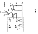
- FIG. 5 is a schematic of a circuit in accordance with the principles of the invention.
- FIG. 6 is a plot of bandgap circuit voltage versus temperature with high temperature compensation in accordance with the principles of the invention.
- FIG. 7 is a plot of bandgap circuit voltage versus temperature with low temperature compensation in accordance with the principles of the invention.
- FIG. 8 is a plot of bandgap circuit voltage versus temperature with high and low temperature compensation in accordance with the principles of the invention.
- FIG. 9 is a schematic of a bandgap circuit in accordance with the principles of the invention.
- Vbe Vbe
- A ( kT/q ) ⁇ [ln( I 1 /I s ) ⁇ ln( I 2 /AI s )]
- a bandgap circuit is formed as part of a CMOS device of the type utilizing CMOS N-well process technology.
- the most usable bipolar transistors available in the CMOS N-well process is the substrate PNP as shown in FIG. 1 in which a single transistor Q 1 is formed by transistors Q 1 ′, Q 1 ′′ which has an area ratio, A, that is twice that of the transistor Q 2 .
- the structure is shown in schematic form in FIG. 2 . All the collectors of transistors Q 1 ′, Q 1 ′′, Q 2 are connected to the chip substrate 101 , i.e., ground. There is direct electrical access to the base and emitter of each transistor Q 1 ′, Q 1 ′′, Q 2 to measure or control Vbe but there is no separate access to the collectors of the transistors Q 1 ′, Q 1 ′′, Q 2 to monitor or control collector current.
- FIG. 3 illustrates a prior art bandgap circuit 301 architecture.
- Bandgap circuit 301 comprises transistor Q 1 and transistor Q 2 .
- the area of transistor Q 1 is selected to be a predetermined multiple A of the area of transistor Q 2 .
- First and second serially connected resistors R 1 , R 2 are connected between an output node Vbandgap and the emitter of transistor Q 2 .
- a third resistor is connected in series between output node Vref and the emitter of transistor Q 1 .
- a differential input amplifier AMP has a first input coupled to a first circuit node disposed between resistors R 1 , R 2 ; and a second input coupled to a second node disposed between resistor R 3 and the emitter of transistor Q 1 .
- Amplifier AMP has its output coupled to the output node bandgap.
- Bandgap voltage and slope with respect to temperature or temperature coefficient, TC are sensitive to certain process and design variables.
- Vbe for a bipolar transistor operating at constant current has a slight bow over temperature.
- the net result is that a plot of bandgap voltage Vref against temperature has a bow as shown by curve 401 in FIG. 4 .
- a simple differential amplifier formed by transistors M 1 , M 2 as shown in FIG. 5 is used and a comparison is made between a near zero temperature coefficient voltage from the bandgap to the negative temperature coefficient of the bandgap Vbe.
- FIG. 5 illustrates a portion of a simplified curvature corrected bandgap circuit in accordance with the principles of the invention.
- Transistor M 1 and transistor M 2 compare the nearly zero temperature coefficient, TC, voltage V 1 (derived from the bandgap) to the Vbe voltage of the unit size bipolar transistor Q 2 in the bandgap. By adjusting the value of V 1 the threshold temperature where the differential pair M 1 , M 2 begins to switch and steer current provided by transistor M 3 into the bandgap is moved. Voltage V 1 is selected to begin adding current at the temperature where the bandgap begins to dip, e.g., 40° C.
- the width/length W/L ratio of transistors M 1 , M 2 will define the amount of differential voltage necessary to switch all of the current from transistor M 2 to transistor M 1 .
- the current I sets the maximum amount of current that can or will be added to the bandgap.
- the comparator/current injection structure can be mirrored for curvature correction of the cold temperature side of the bandgap by providing current removal from the larger or A sized transistor Q 1 of the bandgap circuit.
- the effect of such curvature correction on the cold side is shown by curve 701 in FIG. 7 .
- FIG. 9 A fully compensated bandgap circuit in accordance with the principles of the invention that provides both hot and cold temperature compensation is shown in FIG. 9 .
- the circuit of FIG. 9 shows substantial improvement in performance over a temperature range of interest is ⁇ 40 to 125° C.
- a plot of Vref versus temperature is shown in FIG. 8 as curve 801 .
- the compensated circuit of FIG. 9 includes bandgap circuit 1001 , current injection circuit 1003 and current injection circuit 1005 .
- Bandgap circuit 1001 comprising a transistor Q 2 and a transistor Q 1 .
- the area of transistor Q 1 is selected to be a predetermined multiple A of the area of transistor Q 2 .
- First and second serially connected resistors R 1 , R 2 are connected between an output node Vbandgap and the emitter of transistor Q 2 .
- a third resistor is connected in series between output node Vref and the emitter of transistor Q 1 .
- a differential input amplifier AMP has a first input coupled to a first circuit node disposed between resistors R 1 , R 2 ; and a second input coupled to a second node disposed between resistor R 3 and the emitter of transistor Q 1 .
- Amplifier AMP has its output coupled to the output node Vbandgap.
- a first switchable current source 1003 is coupled to said transistor Q 2 to inject a first current into the emitter of transistor Q 2 .
- the current I inj1 is selected to correct for one of hotter or colder temperatures, more specifically, in the illustrative embodiment, the current I inj1 is injected at higher temperatures when the base emitter voltage across transistor Q 2 to a first predetermined voltage Vset.
- the voltage Vset is determined by a resistance network formed by resistors R 4 , R 5 , R 6 .
- a second switchable current source 1005 is coupled to transistor Q 1 to remove a second current I inj2 into the emitter of transistor Q 1 .
- the second current I inj2 is selected to correct for the other of the hotter or colder temperatures, and more specifically for colder temperatures.
- Bandgap circuit 1001 , and switchable current injection circuits 1003 , 1005 are formed on a single common substrate 1007 .
- the resistors R 4 , R 5 , and R 6 are trimmable resistors and are utilized to select the voltages at which the current sources inject current from switchable current injection circuits 1003 , 1005 into bandgap circuit 1001 .
Abstract
Description
I c =AI s(e (Vbe·q)/kT−1)
where:
- T is temperature in Kelvin;
- A is an area scale;
- Is is dark current for a unit area device (process dependent);
- q is charge on the electron; and
- K is Boltzman's constant.
I c =I s(e (Vbe·q)/kT)
, and
V be=(kT/q)·ln(I c /AI s)
ΔVbe=Vbe| 1 −Vbe| A=(kT/q)·[ln(I 1 /I s)−ln(I 2 /AI s)]
ΔVbe=(kT/q)lnA
Vbandgap=(kT/q)·{ln[((kT/q)·lnA/R 1)/I s]}+(1+R 2 /R 1)(kT/q)·lnA
This is of the form Vref=Vbe+m ΔVbe
Claims (14)
Priority Applications (4)
| Application Number | Priority Date | Filing Date | Title |
|---|---|---|---|
| US12/749,337 US7960961B2 (en) | 2006-06-02 | 2010-03-29 | Bandgap circuit with temperature correction |
| US13/157,761 US8421434B2 (en) | 2006-06-02 | 2011-06-10 | Bandgap circuit with temperature correction |
| US13/863,169 US8941370B2 (en) | 2006-06-02 | 2013-04-15 | Bandgap circuit with temperature correction |
| US14/594,438 US9671800B2 (en) | 2006-06-02 | 2015-01-12 | Bandgap circuit with temperature correction |
Applications Claiming Priority (2)
| Application Number | Priority Date | Filing Date | Title |
|---|---|---|---|
| US11/446,036 US7688054B2 (en) | 2006-06-02 | 2006-06-02 | Bandgap circuit with temperature correction |
| US12/749,337 US7960961B2 (en) | 2006-06-02 | 2010-03-29 | Bandgap circuit with temperature correction |
Related Parent Applications (1)
| Application Number | Title | Priority Date | Filing Date |
|---|---|---|---|
| US11/446,036 Continuation US7688054B2 (en) | 2006-06-02 | 2006-06-02 | Bandgap circuit with temperature correction |
Related Child Applications (1)
| Application Number | Title | Priority Date | Filing Date |
|---|---|---|---|
| US13/157,761 Continuation US8421434B2 (en) | 2006-06-02 | 2011-06-10 | Bandgap circuit with temperature correction |
Publications (2)
| Publication Number | Publication Date |
|---|---|
| US20100181986A1 US20100181986A1 (en) | 2010-07-22 |
| US7960961B2 true US7960961B2 (en) | 2011-06-14 |
Family
ID=38789352
Family Applications (5)
| Application Number | Title | Priority Date | Filing Date |
|---|---|---|---|
| US11/446,036 Expired - Fee Related US7688054B2 (en) | 2006-06-02 | 2006-06-02 | Bandgap circuit with temperature correction |
| US12/749,337 Active US7960961B2 (en) | 2006-06-02 | 2010-03-29 | Bandgap circuit with temperature correction |
| US13/157,761 Active US8421434B2 (en) | 2006-06-02 | 2011-06-10 | Bandgap circuit with temperature correction |
| US13/863,169 Active US8941370B2 (en) | 2006-06-02 | 2013-04-15 | Bandgap circuit with temperature correction |
| US14/594,438 Active US9671800B2 (en) | 2006-06-02 | 2015-01-12 | Bandgap circuit with temperature correction |
Family Applications Before (1)
| Application Number | Title | Priority Date | Filing Date |
|---|---|---|---|
| US11/446,036 Expired - Fee Related US7688054B2 (en) | 2006-06-02 | 2006-06-02 | Bandgap circuit with temperature correction |
Family Applications After (3)
| Application Number | Title | Priority Date | Filing Date |
|---|---|---|---|
| US13/157,761 Active US8421434B2 (en) | 2006-06-02 | 2011-06-10 | Bandgap circuit with temperature correction |
| US13/863,169 Active US8941370B2 (en) | 2006-06-02 | 2013-04-15 | Bandgap circuit with temperature correction |
| US14/594,438 Active US9671800B2 (en) | 2006-06-02 | 2015-01-12 | Bandgap circuit with temperature correction |
Country Status (1)
| Country | Link |
|---|---|
| US (5) | US7688054B2 (en) |
Cited By (4)
| Publication number | Priority date | Publication date | Assignee | Title |
|---|---|---|---|---|
| US20080245237A1 (en) * | 2003-12-30 | 2008-10-09 | Haverstock Thomas B | Coffee infusion press for stackable cups |
| US20120169413A1 (en) * | 2010-12-30 | 2012-07-05 | Stmicroelectronics Inc. | Bandgap voltage reference circuit, system, and method for reduced output curvature |
| US8421434B2 (en) | 2006-06-02 | 2013-04-16 | Dolpan Audio, Llc | Bandgap circuit with temperature correction |
| US9098098B2 (en) | 2012-11-01 | 2015-08-04 | Invensense, Inc. | Curvature-corrected bandgap reference |
Families Citing this family (13)
| Publication number | Priority date | Publication date | Assignee | Title |
|---|---|---|---|---|
| US8427129B2 (en) * | 2007-06-15 | 2013-04-23 | Scott Lawrence Howe | High current drive bandgap based voltage regulator |
| JP5543090B2 (en) * | 2008-08-26 | 2014-07-09 | ピーエスフォー ルクスコ エスエイアールエル | Band gap power supply circuit and starting method thereof |
| JPWO2011016153A1 (en) * | 2009-08-06 | 2013-01-10 | パナソニック株式会社 | Reference voltage generation circuit |
| US8193854B2 (en) * | 2010-01-04 | 2012-06-05 | Hong Kong Applied Science and Technology Research Institute Company, Ltd. | Bi-directional trimming methods and circuits for a precise band-gap reference |
| JP5607963B2 (en) * | 2010-03-19 | 2014-10-15 | スパンション エルエルシー | Reference voltage circuit and semiconductor integrated circuit |
| CN102393783A (en) * | 2011-10-19 | 2012-03-28 | 四川和芯微电子股份有限公司 | Current source circuit and system with high-order temperature compensation |
| TWI502304B (en) * | 2013-06-03 | 2015-10-01 | Advanced Semiconductor Eng | Bandgap reference voltage generating circuit and electronic system using the same |
| US10310528B1 (en) * | 2017-12-06 | 2019-06-04 | Silicon Laboratories Inc. | System and method for correcting offset voltage errors within a band gap circuit |
| CN109343639B (en) * | 2018-11-01 | 2020-09-22 | 西安电子科技大学 | Low-temperature floating band gap reference voltage circuit, method and chip thereof |
| CN109738784B (en) * | 2018-12-17 | 2021-03-30 | 矽力杰半导体技术(杭州)有限公司 | Temperature curve acquisition method of circuit |
| CN109521829B (en) * | 2018-12-25 | 2023-10-31 | 西安航天民芯科技有限公司 | Voltage reference source circuit with full temperature Duan Gaojie temperature compensation |
| CN112034922B (en) * | 2020-11-06 | 2021-01-15 | 成都铱通科技有限公司 | Positive temperature coefficient bias voltage generating circuit with accurate threshold |
| US11762410B2 (en) * | 2021-06-25 | 2023-09-19 | Semiconductor Components Industries, Llc | Voltage reference with temperature-selective second-order temperature compensation |
Citations (10)
| Publication number | Priority date | Publication date | Assignee | Title |
|---|---|---|---|---|
| US5229710A (en) | 1991-04-05 | 1993-07-20 | Siemens Aktiengesellschaft | Cmos band gap reference circuit |
| US5712590A (en) | 1995-12-21 | 1998-01-27 | Dries; Michael F. | Temperature stabilized bandgap voltage reference circuit |
| US6157245A (en) | 1999-03-29 | 2000-12-05 | Texas Instruments Incorporated | Exact curvature-correcting method for bandgap circuits |
| US6218822B1 (en) | 1999-10-13 | 2001-04-17 | National Semiconductor Corporation | CMOS voltage reference with post-assembly curvature trim |
| US6225850B1 (en) | 1998-12-30 | 2001-05-01 | Ion E. Opris | Series resistance compensation in translinear circuits |
| US6642699B1 (en) | 2002-04-29 | 2003-11-04 | Ami Semiconductor, Inc. | Bandgap voltage reference using differential pairs to perform temperature curvature compensation |
| US6677808B1 (en) | 2002-08-16 | 2004-01-13 | National Semiconductor Corporation | CMOS adjustable bandgap reference with low power and low voltage performance |
| US6724176B1 (en) | 2002-10-29 | 2004-04-20 | National Semiconductor Corporation | Low power, low noise band-gap circuit using second order curvature correction |
| US20050122091A1 (en) * | 2003-12-09 | 2005-06-09 | Analog Devices, Inc. | Bandgap voltage reference |
| US7224209B2 (en) | 2005-03-03 | 2007-05-29 | Etron Technology, Inc. | Speed-up circuit for initiation of proportional to absolute temperature biasing circuits |
Family Cites Families (45)
| Publication number | Priority date | Publication date | Assignee | Title |
|---|---|---|---|---|
| DE1813330C3 (en) | 1968-12-07 | 1978-06-01 | Demag Ag, 4100 Duisburg | Device for continuous measurement of the temperature on metal strands, especially when continuously casting steel |
| US3678486A (en) | 1969-10-16 | 1972-07-18 | Goodyear Tire & Rubber | Monitoring system |
| GB1421620A (en) | 1973-06-12 | 1976-01-21 | Ferranti Ltd | Inertial navigation apparatus |
| US4004462A (en) | 1974-06-07 | 1977-01-25 | National Semiconductor Corporation | Temperature transducer |
| US3903395A (en) | 1974-06-12 | 1975-09-02 | Gen Electric | Temperature control system |
| JPS5913052B2 (en) | 1975-07-25 | 1984-03-27 | 日本電気株式会社 | Reference voltage source circuit |
| DE2933874C2 (en) | 1978-08-24 | 1986-07-17 | Hochiki Corp., Tokio/Tokyo | Sensing device for sensing temperature differences between two points |
| US4317054A (en) | 1980-02-07 | 1982-02-23 | Mostek Corporation | Bandgap voltage reference employing sub-surface current using a standard CMOS process |
| US4603291A (en) * | 1984-06-26 | 1986-07-29 | Linear Technology Corporation | Nonlinearity correction circuit for bandgap reference |
| CH661600A5 (en) | 1985-01-17 | 1987-07-31 | Centre Electron Horloger | REFERENCE VOLTAGE SOURCE. |
| US4939442A (en) * | 1989-03-30 | 1990-07-03 | Texas Instruments Incorporated | Bandgap voltage reference and method with further temperature correction |
| US5053640A (en) * | 1989-10-25 | 1991-10-01 | Silicon General, Inc. | Bandgap voltage reference circuit |
| US5228114A (en) | 1990-10-30 | 1993-07-13 | Tokyo Electron Sagami Limited | Heat-treating apparatus with batch scheme having improved heat controlling capability |
| JPH08511872A (en) | 1993-06-22 | 1996-12-10 | ハネウエル・インコーポレーテッド | Double matched current sink full temperature circuit |
| SG80573A1 (en) | 1997-06-02 | 2001-05-22 | Motorola Inc | Integrated temperature sensor |
| US5982221A (en) | 1997-08-13 | 1999-11-09 | Analog Devices, Inc. | Switched current temperature sensor circuit with compounded ΔVBE |
| US5867012A (en) | 1997-08-14 | 1999-02-02 | Analog Devices, Inc. | Switching bandgap reference circuit with compounded ΔV.sub.βΕ |
| US6037833A (en) * | 1997-11-10 | 2000-03-14 | Philips Electronics North America Corporation | Generator for generating voltage proportional to absolute temperature |
| US6252209B1 (en) | 1999-01-21 | 2001-06-26 | Andigilog, Inc. | Adaptive temperature control circuit with PWM output |
| US6411158B1 (en) | 1999-09-03 | 2002-06-25 | Conexant Systems, Inc. | Bandgap reference voltage with low noise sensitivity |
| US6329804B1 (en) * | 1999-10-13 | 2001-12-11 | National Semiconductor Corporation | Slope and level trim DAC for voltage reference |
| GB0011541D0 (en) | 2000-05-12 | 2000-06-28 | Sgs Thomson Microelectronics | Generation of a voltage proportional to temperature with a negative variation |
| US6466081B1 (en) | 2000-11-08 | 2002-10-15 | Applied Micro Circuits Corporation | Temperature stable CMOS device |
| US6362612B1 (en) | 2001-01-23 | 2002-03-26 | Larry L. Harris | Bandgap voltage reference circuit |
| JP3669307B2 (en) | 2001-08-03 | 2005-07-06 | ソニー株式会社 | Start-up circuit |
| JP3721119B2 (en) | 2001-11-08 | 2005-11-30 | 株式会社東芝 | Temperature sensor |
| US6556155B1 (en) * | 2002-02-19 | 2003-04-29 | Texas Advanced Optoelectronic Solutions, Inc. | Method and integrated circuit for temperature coefficient compensation |
| JP2004146576A (en) | 2002-10-24 | 2004-05-20 | Renesas Technology Corp | Semiconductor temperature measuring circuit |
| US6891358B2 (en) * | 2002-12-27 | 2005-05-10 | Analog Devices, Inc. | Bandgap voltage reference circuit with high power supply rejection ratio (PSRR) and curvature correction |
| US7857510B2 (en) | 2003-11-08 | 2010-12-28 | Carl F Liepold | Temperature sensing circuit |
| US7010440B1 (en) | 2003-11-25 | 2006-03-07 | Analog Devices, Inc. | Method and a measuring circuit for determining temperature from a PN junction temperature sensor, and a temperature sensing circuit comprising the measuring circuit and a PN junction |
| US7030584B1 (en) | 2004-09-27 | 2006-04-18 | Andigilog, Inc. | Controller arrangement |
| US7276867B2 (en) | 2004-11-10 | 2007-10-02 | Andigilog, Inc. | Controller arrangement with adaptive non-overlapping commutation |
| US7064510B2 (en) | 2004-11-10 | 2006-06-20 | Andigilog, Inc. | Controller arrangement with automatic power down |
| US7237951B2 (en) | 2005-03-31 | 2007-07-03 | Andigilog, Inc. | Substrate based temperature sensing |
| US20070052473A1 (en) * | 2005-09-02 | 2007-03-08 | Standard Microsystems Corporation | Perfectly curvature corrected bandgap reference |
| US7688054B2 (en) | 2006-06-02 | 2010-03-30 | David Cave | Bandgap circuit with temperature correction |
| US7482797B2 (en) | 2006-06-02 | 2009-01-27 | Dolpan Audio, Llc | Trimmable bandgap circuit |
| US7592677B2 (en) | 2006-07-11 | 2009-09-22 | David Cave | Over-voltage protected semiconductor device and fabrication |
| US7468873B2 (en) | 2006-07-11 | 2008-12-23 | Dolpan Audio, Llc | Over-voltage protected semiconductor device |
| US7576396B2 (en) | 2006-07-25 | 2009-08-18 | Dolpan Audio, Llc | Synchronous substrate injection clamp |
| US8004337B2 (en) | 2007-01-30 | 2011-08-23 | Dolpan Audio, Llc | Digital delay circuit |
| US7538505B2 (en) | 2007-05-01 | 2009-05-26 | Alberkrack Jade H | Noise suppresion suppression for hall sensor arrangements |
| US7636010B2 (en) * | 2007-09-03 | 2009-12-22 | Elite Semiconductor Memory Technology Inc. | Process independent curvature compensation scheme for bandgap reference |
| US20090243113A1 (en) | 2008-03-31 | 2009-10-01 | Andigilog, Inc. | Semiconductor structure |
-
2006
- 2006-06-02 US US11/446,036 patent/US7688054B2/en not_active Expired - Fee Related
-
2010
- 2010-03-29 US US12/749,337 patent/US7960961B2/en active Active
-
2011
- 2011-06-10 US US13/157,761 patent/US8421434B2/en active Active
-
2013
- 2013-04-15 US US13/863,169 patent/US8941370B2/en active Active
-
2015
- 2015-01-12 US US14/594,438 patent/US9671800B2/en active Active
Patent Citations (10)
| Publication number | Priority date | Publication date | Assignee | Title |
|---|---|---|---|---|
| US5229710A (en) | 1991-04-05 | 1993-07-20 | Siemens Aktiengesellschaft | Cmos band gap reference circuit |
| US5712590A (en) | 1995-12-21 | 1998-01-27 | Dries; Michael F. | Temperature stabilized bandgap voltage reference circuit |
| US6225850B1 (en) | 1998-12-30 | 2001-05-01 | Ion E. Opris | Series resistance compensation in translinear circuits |
| US6157245A (en) | 1999-03-29 | 2000-12-05 | Texas Instruments Incorporated | Exact curvature-correcting method for bandgap circuits |
| US6218822B1 (en) | 1999-10-13 | 2001-04-17 | National Semiconductor Corporation | CMOS voltage reference with post-assembly curvature trim |
| US6642699B1 (en) | 2002-04-29 | 2003-11-04 | Ami Semiconductor, Inc. | Bandgap voltage reference using differential pairs to perform temperature curvature compensation |
| US6677808B1 (en) | 2002-08-16 | 2004-01-13 | National Semiconductor Corporation | CMOS adjustable bandgap reference with low power and low voltage performance |
| US6724176B1 (en) | 2002-10-29 | 2004-04-20 | National Semiconductor Corporation | Low power, low noise band-gap circuit using second order curvature correction |
| US20050122091A1 (en) * | 2003-12-09 | 2005-06-09 | Analog Devices, Inc. | Bandgap voltage reference |
| US7224209B2 (en) | 2005-03-03 | 2007-05-29 | Etron Technology, Inc. | Speed-up circuit for initiation of proportional to absolute temperature biasing circuits |
Cited By (7)
| Publication number | Priority date | Publication date | Assignee | Title |
|---|---|---|---|---|
| US20080245237A1 (en) * | 2003-12-30 | 2008-10-09 | Haverstock Thomas B | Coffee infusion press for stackable cups |
| US8421434B2 (en) | 2006-06-02 | 2013-04-16 | Dolpan Audio, Llc | Bandgap circuit with temperature correction |
| US8941370B2 (en) | 2006-06-02 | 2015-01-27 | Doplan Audio, LLC | Bandgap circuit with temperature correction |
| US9671800B2 (en) | 2006-06-02 | 2017-06-06 | Ol Security Limited Liability Company | Bandgap circuit with temperature correction |
| US20120169413A1 (en) * | 2010-12-30 | 2012-07-05 | Stmicroelectronics Inc. | Bandgap voltage reference circuit, system, and method for reduced output curvature |
| US8648648B2 (en) * | 2010-12-30 | 2014-02-11 | Stmicroelectronics, Inc. | Bandgap voltage reference circuit, system, and method for reduced output curvature |
| US9098098B2 (en) | 2012-11-01 | 2015-08-04 | Invensense, Inc. | Curvature-corrected bandgap reference |
Also Published As
| Publication number | Publication date |
|---|---|
| US20070279029A1 (en) | 2007-12-06 |
| US20150123643A1 (en) | 2015-05-07 |
| US20100181986A1 (en) | 2010-07-22 |
| US7688054B2 (en) | 2010-03-30 |
| US8941370B2 (en) | 2015-01-27 |
| US8421434B2 (en) | 2013-04-16 |
| US20110234197A1 (en) | 2011-09-29 |
| US20130285637A1 (en) | 2013-10-31 |
| US9671800B2 (en) | 2017-06-06 |
Similar Documents
| Publication | Publication Date | Title |
|---|---|---|
| US7960961B2 (en) | Bandgap circuit with temperature correction | |
| US7482797B2 (en) | Trimmable bandgap circuit | |
| US8629712B2 (en) | Operational amplifier | |
| US9347836B2 (en) | Dynamic voltage reference for sampling delta based temperature sensor | |
| US7148672B1 (en) | Low-voltage bandgap reference circuit with startup control | |
| KR101829416B1 (en) | Compensated bandgap | |
| US7710096B2 (en) | Reference circuit | |
| US8405447B2 (en) | Semiconductor temperature sensor using bandgap generator circuit | |
| US10296026B2 (en) | Low noise reference voltage generator and load regulator | |
| US6870421B2 (en) | Temperature characteristic compensation apparatus | |
| US7170334B2 (en) | Switched current temperature sensing circuit and method to correct errors due to beta and series resistance | |
| US10190922B2 (en) | Method and apparatus for calibrating a sensor | |
| US20060056485A1 (en) | Linear integrated circuit temperature sensor apparatus with adjustable gain and offset | |
| US20080061865A1 (en) | Apparatus and method for providing a temperature dependent output signal | |
| CN113168200B (en) | Precision bandgap reference with trim adjustment | |
| US20070040543A1 (en) | Bandgap reference circuit | |
| US20130170520A1 (en) | Temperature sensor for image sensors | |
| US6137341A (en) | Temperature sensor to run from power supply, 0.9 to 12 volts | |
| US7248098B1 (en) | Curvature corrected bandgap circuit | |
| US7570090B2 (en) | Fast power-on detect circuit with accurate trip-points | |
| US6946825B2 (en) | Bandgap voltage generator with a bipolar assembly and a mirror assembly | |
| US20080106326A1 (en) | Reference voltage circuit and method for providing a reference voltage | |
| CN115357086B (en) | Band gap reference circuit, operation method thereof and electronic device | |
| WO2020165250A1 (en) | Threshold detector of a power on reset circuit with improved accuracy for switching levels over temperature variations | |
| JP2000065872A (en) | Voltage detection circuit |
Legal Events
| Date | Code | Title | Description |
|---|---|---|---|
| AS | Assignment |
Owner name: ANDIGILOG, INC., ARIZONA Free format text: ASSIGNMENT OF ASSIGNORS INTEREST;ASSIGNOR:CAVE, DAVID;REEL/FRAME:025191/0607 Effective date: 20060601 Owner name: DOLPAN AUDIO, LLC, DELAWARE Free format text: ASSIGNMENT OF ASSIGNORS INTEREST;ASSIGNOR:ANDIGILOG, INC.;REEL/FRAME:025191/0546 Effective date: 20080919 |
|
| STCF | Information on status: patent grant |
Free format text: PATENTED CASE |
|
| CC | Certificate of correction | ||
| CC | Certificate of correction | ||
| FPAY | Fee payment |
Year of fee payment: 4 |
|
| AS | Assignment |
Owner name: OL SECURITY LIMITED LIABILITY COMPANY, DELAWARE Free format text: MERGER;ASSIGNOR:DOLPAN AUDIO, LLC;REEL/FRAME:037347/0184 Effective date: 20150826 |
|
| MAFP | Maintenance fee payment |
Free format text: PAYMENT OF MAINTENANCE FEE, 8TH YEAR, LARGE ENTITY (ORIGINAL EVENT CODE: M1552); ENTITY STATUS OF PATENT OWNER: LARGE ENTITY Year of fee payment: 8 |
|
| MAFP | Maintenance fee payment |
Free format text: PAYMENT OF MAINTENANCE FEE, 12TH YEAR, LARGE ENTITY (ORIGINAL EVENT CODE: M1553); ENTITY STATUS OF PATENT OWNER: LARGE ENTITY Year of fee payment: 12 |