US7964962B2 - Method of manufacturing a semiconductor apparatus - Google Patents
Method of manufacturing a semiconductor apparatus Download PDFInfo
- Publication number
- US7964962B2 US7964962B2 US12/173,245 US17324508A US7964962B2 US 7964962 B2 US7964962 B2 US 7964962B2 US 17324508 A US17324508 A US 17324508A US 7964962 B2 US7964962 B2 US 7964962B2
- Authority
- US
- United States
- Prior art keywords
- semiconductor
- semiconductor chip
- wired
- wired board
- electrode pads
- Prior art date
- Legal status (The legal status is an assumption and is not a legal conclusion. Google has not performed a legal analysis and makes no representation as to the accuracy of the status listed.)
- Expired - Fee Related, expires
Links
Images


Classifications
-
- H—ELECTRICITY
- H01—ELECTRIC ELEMENTS
- H01L—SEMICONDUCTOR DEVICES NOT COVERED BY CLASS H10
- H01L23/00—Details of semiconductor or other solid state devices
- H01L23/48—Arrangements for conducting electric current to or from the solid state body in operation, e.g. leads, terminal arrangements ; Selection of materials therefor
-
- H—ELECTRICITY
- H01—ELECTRIC ELEMENTS
- H01L—SEMICONDUCTOR DEVICES NOT COVERED BY CLASS H10
- H01L21/00—Processes or apparatus adapted for the manufacture or treatment of semiconductor or solid state devices or of parts thereof
- H01L21/02—Manufacture or treatment of semiconductor devices or of parts thereof
- H01L21/04—Manufacture or treatment of semiconductor devices or of parts thereof the devices having at least one potential-jump barrier or surface barrier, e.g. PN junction, depletion layer or carrier concentration layer
- H01L21/50—Assembly of semiconductor devices using processes or apparatus not provided for in a single one of the subgroups H01L21/06 - H01L21/326, e.g. sealing of a cap to a base of a container
- H01L21/56—Encapsulations, e.g. encapsulation layers, coatings
- H01L21/561—Batch processing
-
- H—ELECTRICITY
- H01—ELECTRIC ELEMENTS
- H01L—SEMICONDUCTOR DEVICES NOT COVERED BY CLASS H10
- H01L21/00—Processes or apparatus adapted for the manufacture or treatment of semiconductor or solid state devices or of parts thereof
- H01L21/67—Apparatus specially adapted for handling semiconductor or electric solid state devices during manufacture or treatment thereof; Apparatus specially adapted for handling wafers during manufacture or treatment of semiconductor or electric solid state devices or components ; Apparatus not specifically provided for elsewhere
- H01L21/683—Apparatus specially adapted for handling semiconductor or electric solid state devices during manufacture or treatment thereof; Apparatus specially adapted for handling wafers during manufacture or treatment of semiconductor or electric solid state devices or components ; Apparatus not specifically provided for elsewhere for supporting or gripping
- H01L21/6835—Apparatus specially adapted for handling semiconductor or electric solid state devices during manufacture or treatment thereof; Apparatus specially adapted for handling wafers during manufacture or treatment of semiconductor or electric solid state devices or components ; Apparatus not specifically provided for elsewhere for supporting or gripping using temporarily an auxiliary support
- H01L21/6836—Wafer tapes, e.g. grinding or dicing support tapes
-
- H—ELECTRICITY
- H01—ELECTRIC ELEMENTS
- H01L—SEMICONDUCTOR DEVICES NOT COVERED BY CLASS H10
- H01L23/00—Details of semiconductor or other solid state devices
- H01L23/12—Mountings, e.g. non-detachable insulating substrates
- H01L23/13—Mountings, e.g. non-detachable insulating substrates characterised by the shape
-
- H—ELECTRICITY
- H01—ELECTRIC ELEMENTS
- H01L—SEMICONDUCTOR DEVICES NOT COVERED BY CLASS H10
- H01L23/00—Details of semiconductor or other solid state devices
- H01L23/28—Encapsulations, e.g. encapsulating layers, coatings, e.g. for protection
- H01L23/31—Encapsulations, e.g. encapsulating layers, coatings, e.g. for protection characterised by the arrangement or shape
- H01L23/3107—Encapsulations, e.g. encapsulating layers, coatings, e.g. for protection characterised by the arrangement or shape the device being completely enclosed
- H01L23/3121—Encapsulations, e.g. encapsulating layers, coatings, e.g. for protection characterised by the arrangement or shape the device being completely enclosed a substrate forming part of the encapsulation
- H01L23/3128—Encapsulations, e.g. encapsulating layers, coatings, e.g. for protection characterised by the arrangement or shape the device being completely enclosed a substrate forming part of the encapsulation the substrate having spherical bumps for external connection
-
- H—ELECTRICITY
- H01—ELECTRIC ELEMENTS
- H01L—SEMICONDUCTOR DEVICES NOT COVERED BY CLASS H10
- H01L23/00—Details of semiconductor or other solid state devices
- H01L23/48—Arrangements for conducting electric current to or from the solid state body in operation, e.g. leads, terminal arrangements ; Selection of materials therefor
- H01L23/488—Arrangements for conducting electric current to or from the solid state body in operation, e.g. leads, terminal arrangements ; Selection of materials therefor consisting of soldered or bonded constructions
- H01L23/498—Leads, i.e. metallisations or lead-frames on insulating substrates, e.g. chip carriers
- H01L23/49811—Additional leads joined to the metallisation on the insulating substrate, e.g. pins, bumps, wires, flat leads
- H01L23/49816—Spherical bumps on the substrate for external connection, e.g. ball grid arrays [BGA]
-
- H—ELECTRICITY
- H01—ELECTRIC ELEMENTS
- H01L—SEMICONDUCTOR DEVICES NOT COVERED BY CLASS H10
- H01L24/00—Arrangements for connecting or disconnecting semiconductor or solid-state bodies; Methods or apparatus related thereto
- H01L24/01—Means for bonding being attached to, or being formed on, the surface to be connected, e.g. chip-to-package, die-attach, "first-level" interconnects; Manufacturing methods related thereto
- H01L24/02—Bonding areas ; Manufacturing methods related thereto
- H01L24/04—Structure, shape, material or disposition of the bonding areas prior to the connecting process
- H01L24/06—Structure, shape, material or disposition of the bonding areas prior to the connecting process of a plurality of bonding areas
-
- H—ELECTRICITY
- H01—ELECTRIC ELEMENTS
- H01L—SEMICONDUCTOR DEVICES NOT COVERED BY CLASS H10
- H01L24/00—Arrangements for connecting or disconnecting semiconductor or solid-state bodies; Methods or apparatus related thereto
- H01L24/01—Means for bonding being attached to, or being formed on, the surface to be connected, e.g. chip-to-package, die-attach, "first-level" interconnects; Manufacturing methods related thereto
- H01L24/10—Bump connectors ; Manufacturing methods related thereto
- H01L24/15—Structure, shape, material or disposition of the bump connectors after the connecting process
- H01L24/17—Structure, shape, material or disposition of the bump connectors after the connecting process of a plurality of bump connectors
-
- H—ELECTRICITY
- H01—ELECTRIC ELEMENTS
- H01L—SEMICONDUCTOR DEVICES NOT COVERED BY CLASS H10
- H01L24/00—Arrangements for connecting or disconnecting semiconductor or solid-state bodies; Methods or apparatus related thereto
- H01L24/01—Means for bonding being attached to, or being formed on, the surface to be connected, e.g. chip-to-package, die-attach, "first-level" interconnects; Manufacturing methods related thereto
- H01L24/26—Layer connectors, e.g. plate connectors, solder or adhesive layers; Manufacturing methods related thereto
- H01L24/27—Manufacturing methods
-
- H—ELECTRICITY
- H01—ELECTRIC ELEMENTS
- H01L—SEMICONDUCTOR DEVICES NOT COVERED BY CLASS H10
- H01L24/00—Arrangements for connecting or disconnecting semiconductor or solid-state bodies; Methods or apparatus related thereto
- H01L24/93—Batch processes
- H01L24/94—Batch processes at wafer-level, i.e. with connecting carried out on a wafer comprising a plurality of undiced individual devices
-
- H—ELECTRICITY
- H01—ELECTRIC ELEMENTS
- H01L—SEMICONDUCTOR DEVICES NOT COVERED BY CLASS H10
- H01L2221/00—Processes or apparatus adapted for the manufacture or treatment of semiconductor or solid state devices or of parts thereof covered by H01L21/00
- H01L2221/67—Apparatus for handling semiconductor or electric solid state devices during manufacture or treatment thereof; Apparatus for handling wafers during manufacture or treatment of semiconductor or electric solid state devices or components; Apparatus not specifically provided for elsewhere
- H01L2221/683—Apparatus for handling semiconductor or electric solid state devices during manufacture or treatment thereof; Apparatus for handling wafers during manufacture or treatment of semiconductor or electric solid state devices or components; Apparatus not specifically provided for elsewhere for supporting or gripping
- H01L2221/68304—Apparatus for handling semiconductor or electric solid state devices during manufacture or treatment thereof; Apparatus for handling wafers during manufacture or treatment of semiconductor or electric solid state devices or components; Apparatus not specifically provided for elsewhere for supporting or gripping using temporarily an auxiliary support
- H01L2221/68327—Apparatus for handling semiconductor or electric solid state devices during manufacture or treatment thereof; Apparatus for handling wafers during manufacture or treatment of semiconductor or electric solid state devices or components; Apparatus not specifically provided for elsewhere for supporting or gripping using temporarily an auxiliary support used during dicing or grinding
-
- H—ELECTRICITY
- H01—ELECTRIC ELEMENTS
- H01L—SEMICONDUCTOR DEVICES NOT COVERED BY CLASS H10
- H01L2221/00—Processes or apparatus adapted for the manufacture or treatment of semiconductor or solid state devices or of parts thereof covered by H01L21/00
- H01L2221/67—Apparatus for handling semiconductor or electric solid state devices during manufacture or treatment thereof; Apparatus for handling wafers during manufacture or treatment of semiconductor or electric solid state devices or components; Apparatus not specifically provided for elsewhere
- H01L2221/683—Apparatus for handling semiconductor or electric solid state devices during manufacture or treatment thereof; Apparatus for handling wafers during manufacture or treatment of semiconductor or electric solid state devices or components; Apparatus not specifically provided for elsewhere for supporting or gripping
- H01L2221/68304—Apparatus for handling semiconductor or electric solid state devices during manufacture or treatment thereof; Apparatus for handling wafers during manufacture or treatment of semiconductor or electric solid state devices or components; Apparatus not specifically provided for elsewhere for supporting or gripping using temporarily an auxiliary support
- H01L2221/68381—Details of chemical or physical process used for separating the auxiliary support from a device or wafer
-
- H—ELECTRICITY
- H01—ELECTRIC ELEMENTS
- H01L—SEMICONDUCTOR DEVICES NOT COVERED BY CLASS H10
- H01L2223/00—Details relating to semiconductor or other solid state devices covered by the group H01L23/00
- H01L2223/544—Marks applied to semiconductor devices or parts
- H01L2223/54473—Marks applied to semiconductor devices or parts for use after dicing
- H01L2223/54486—Located on package parts, e.g. encapsulation, leads, package substrate
-
- H—ELECTRICITY
- H01—ELECTRIC ELEMENTS
- H01L—SEMICONDUCTOR DEVICES NOT COVERED BY CLASS H10
- H01L2224/00—Indexing scheme for arrangements for connecting or disconnecting semiconductor or solid-state bodies and methods related thereto as covered by H01L24/00
- H01L2224/01—Means for bonding being attached to, or being formed on, the surface to be connected, e.g. chip-to-package, die-attach, "first-level" interconnects; Manufacturing methods related thereto
- H01L2224/02—Bonding areas; Manufacturing methods related thereto
- H01L2224/04—Structure, shape, material or disposition of the bonding areas prior to the connecting process
- H01L2224/0401—Bonding areas specifically adapted for bump connectors, e.g. under bump metallisation [UBM]
-
- H—ELECTRICITY
- H01—ELECTRIC ELEMENTS
- H01L—SEMICONDUCTOR DEVICES NOT COVERED BY CLASS H10
- H01L2224/00—Indexing scheme for arrangements for connecting or disconnecting semiconductor or solid-state bodies and methods related thereto as covered by H01L24/00
- H01L2224/01—Means for bonding being attached to, or being formed on, the surface to be connected, e.g. chip-to-package, die-attach, "first-level" interconnects; Manufacturing methods related thereto
- H01L2224/02—Bonding areas; Manufacturing methods related thereto
- H01L2224/04—Structure, shape, material or disposition of the bonding areas prior to the connecting process
- H01L2224/04042—Bonding areas specifically adapted for wire connectors, e.g. wirebond pads
-
- H—ELECTRICITY
- H01—ELECTRIC ELEMENTS
- H01L—SEMICONDUCTOR DEVICES NOT COVERED BY CLASS H10
- H01L2224/00—Indexing scheme for arrangements for connecting or disconnecting semiconductor or solid-state bodies and methods related thereto as covered by H01L24/00
- H01L2224/01—Means for bonding being attached to, or being formed on, the surface to be connected, e.g. chip-to-package, die-attach, "first-level" interconnects; Manufacturing methods related thereto
- H01L2224/02—Bonding areas; Manufacturing methods related thereto
- H01L2224/04—Structure, shape, material or disposition of the bonding areas prior to the connecting process
- H01L2224/06—Structure, shape, material or disposition of the bonding areas prior to the connecting process of a plurality of bonding areas
- H01L2224/061—Disposition
- H01L2224/0612—Layout
- H01L2224/0613—Square or rectangular array
- H01L2224/06134—Square or rectangular array covering only portions of the surface to be connected
- H01L2224/06136—Covering only the central area of the surface to be connected, i.e. central arrangements
-
- H—ELECTRICITY
- H01—ELECTRIC ELEMENTS
- H01L—SEMICONDUCTOR DEVICES NOT COVERED BY CLASS H10
- H01L2224/00—Indexing scheme for arrangements for connecting or disconnecting semiconductor or solid-state bodies and methods related thereto as covered by H01L24/00
- H01L2224/01—Means for bonding being attached to, or being formed on, the surface to be connected, e.g. chip-to-package, die-attach, "first-level" interconnects; Manufacturing methods related thereto
- H01L2224/10—Bump connectors; Manufacturing methods related thereto
- H01L2224/11—Manufacturing methods
- H01L2224/113—Manufacturing methods by local deposition of the material of the bump connector
- H01L2224/1133—Manufacturing methods by local deposition of the material of the bump connector in solid form
- H01L2224/1134—Stud bumping, i.e. using a wire-bonding apparatus
-
- H—ELECTRICITY
- H01—ELECTRIC ELEMENTS
- H01L—SEMICONDUCTOR DEVICES NOT COVERED BY CLASS H10
- H01L2224/00—Indexing scheme for arrangements for connecting or disconnecting semiconductor or solid-state bodies and methods related thereto as covered by H01L24/00
- H01L2224/01—Means for bonding being attached to, or being formed on, the surface to be connected, e.g. chip-to-package, die-attach, "first-level" interconnects; Manufacturing methods related thereto
- H01L2224/10—Bump connectors; Manufacturing methods related thereto
- H01L2224/12—Structure, shape, material or disposition of the bump connectors prior to the connecting process
- H01L2224/13—Structure, shape, material or disposition of the bump connectors prior to the connecting process of an individual bump connector
- H01L2224/13001—Core members of the bump connector
- H01L2224/13099—Material
-
- H—ELECTRICITY
- H01—ELECTRIC ELEMENTS
- H01L—SEMICONDUCTOR DEVICES NOT COVERED BY CLASS H10
- H01L2224/00—Indexing scheme for arrangements for connecting or disconnecting semiconductor or solid-state bodies and methods related thereto as covered by H01L24/00
- H01L2224/01—Means for bonding being attached to, or being formed on, the surface to be connected, e.g. chip-to-package, die-attach, "first-level" interconnects; Manufacturing methods related thereto
- H01L2224/10—Bump connectors; Manufacturing methods related thereto
- H01L2224/15—Structure, shape, material or disposition of the bump connectors after the connecting process
- H01L2224/16—Structure, shape, material or disposition of the bump connectors after the connecting process of an individual bump connector
- H01L2224/1601—Structure
-
- H—ELECTRICITY
- H01—ELECTRIC ELEMENTS
- H01L—SEMICONDUCTOR DEVICES NOT COVERED BY CLASS H10
- H01L2224/00—Indexing scheme for arrangements for connecting or disconnecting semiconductor or solid-state bodies and methods related thereto as covered by H01L24/00
- H01L2224/01—Means for bonding being attached to, or being formed on, the surface to be connected, e.g. chip-to-package, die-attach, "first-level" interconnects; Manufacturing methods related thereto
- H01L2224/10—Bump connectors; Manufacturing methods related thereto
- H01L2224/15—Structure, shape, material or disposition of the bump connectors after the connecting process
- H01L2224/16—Structure, shape, material or disposition of the bump connectors after the connecting process of an individual bump connector
- H01L2224/161—Disposition
- H01L2224/16151—Disposition the bump connector connecting between a semiconductor or solid-state body and an item not being a semiconductor or solid-state body, e.g. chip-to-substrate, chip-to-passive
- H01L2224/16221—Disposition the bump connector connecting between a semiconductor or solid-state body and an item not being a semiconductor or solid-state body, e.g. chip-to-substrate, chip-to-passive the body and the item being stacked
- H01L2224/16225—Disposition the bump connector connecting between a semiconductor or solid-state body and an item not being a semiconductor or solid-state body, e.g. chip-to-substrate, chip-to-passive the body and the item being stacked the item being non-metallic, e.g. insulating substrate with or without metallisation
- H01L2224/16237—Disposition the bump connector connecting between a semiconductor or solid-state body and an item not being a semiconductor or solid-state body, e.g. chip-to-substrate, chip-to-passive the body and the item being stacked the item being non-metallic, e.g. insulating substrate with or without metallisation the bump connector connecting to a bonding area disposed in a recess of the surface of the item
-
- H—ELECTRICITY
- H01—ELECTRIC ELEMENTS
- H01L—SEMICONDUCTOR DEVICES NOT COVERED BY CLASS H10
- H01L2224/00—Indexing scheme for arrangements for connecting or disconnecting semiconductor or solid-state bodies and methods related thereto as covered by H01L24/00
- H01L2224/01—Means for bonding being attached to, or being formed on, the surface to be connected, e.g. chip-to-package, die-attach, "first-level" interconnects; Manufacturing methods related thereto
- H01L2224/26—Layer connectors, e.g. plate connectors, solder or adhesive layers; Manufacturing methods related thereto
- H01L2224/27—Manufacturing methods
- H01L2224/274—Manufacturing methods by blanket deposition of the material of the layer connector
-
- H—ELECTRICITY
- H01—ELECTRIC ELEMENTS
- H01L—SEMICONDUCTOR DEVICES NOT COVERED BY CLASS H10
- H01L2224/00—Indexing scheme for arrangements for connecting or disconnecting semiconductor or solid-state bodies and methods related thereto as covered by H01L24/00
- H01L2224/01—Means for bonding being attached to, or being formed on, the surface to be connected, e.g. chip-to-package, die-attach, "first-level" interconnects; Manufacturing methods related thereto
- H01L2224/26—Layer connectors, e.g. plate connectors, solder or adhesive layers; Manufacturing methods related thereto
- H01L2224/31—Structure, shape, material or disposition of the layer connectors after the connecting process
- H01L2224/32—Structure, shape, material or disposition of the layer connectors after the connecting process of an individual layer connector
- H01L2224/321—Disposition
- H01L2224/32151—Disposition the layer connector connecting between a semiconductor or solid-state body and an item not being a semiconductor or solid-state body, e.g. chip-to-substrate, chip-to-passive
- H01L2224/32221—Disposition the layer connector connecting between a semiconductor or solid-state body and an item not being a semiconductor or solid-state body, e.g. chip-to-substrate, chip-to-passive the body and the item being stacked
- H01L2224/32225—Disposition the layer connector connecting between a semiconductor or solid-state body and an item not being a semiconductor or solid-state body, e.g. chip-to-substrate, chip-to-passive the body and the item being stacked the item being non-metallic, e.g. insulating substrate with or without metallisation
-
- H—ELECTRICITY
- H01—ELECTRIC ELEMENTS
- H01L—SEMICONDUCTOR DEVICES NOT COVERED BY CLASS H10
- H01L2224/00—Indexing scheme for arrangements for connecting or disconnecting semiconductor or solid-state bodies and methods related thereto as covered by H01L24/00
- H01L2224/73—Means for bonding being of different types provided for in two or more of groups H01L2224/10, H01L2224/18, H01L2224/26, H01L2224/34, H01L2224/42, H01L2224/50, H01L2224/63, H01L2224/71
- H01L2224/732—Location after the connecting process
- H01L2224/73201—Location after the connecting process on the same surface
- H01L2224/73203—Bump and layer connectors
- H01L2224/73204—Bump and layer connectors the bump connector being embedded into the layer connector
-
- H—ELECTRICITY
- H01—ELECTRIC ELEMENTS
- H01L—SEMICONDUCTOR DEVICES NOT COVERED BY CLASS H10
- H01L2224/00—Indexing scheme for arrangements for connecting or disconnecting semiconductor or solid-state bodies and methods related thereto as covered by H01L24/00
- H01L2224/74—Apparatus for manufacturing arrangements for connecting or disconnecting semiconductor or solid-state bodies and for methods related thereto
- H01L2224/75—Apparatus for connecting with bump connectors or layer connectors
-
- H—ELECTRICITY
- H01—ELECTRIC ELEMENTS
- H01L—SEMICONDUCTOR DEVICES NOT COVERED BY CLASS H10
- H01L2224/00—Indexing scheme for arrangements for connecting or disconnecting semiconductor or solid-state bodies and methods related thereto as covered by H01L24/00
- H01L2224/80—Methods for connecting semiconductor or other solid state bodies using means for bonding being attached to, or being formed on, the surface to be connected
- H01L2224/81—Methods for connecting semiconductor or other solid state bodies using means for bonding being attached to, or being formed on, the surface to be connected using a bump connector
- H01L2224/8119—Arrangement of the bump connectors prior to mounting
- H01L2224/81193—Arrangement of the bump connectors prior to mounting wherein the bump connectors are disposed on both the semiconductor or solid-state body and another item or body to be connected to the semiconductor or solid-state body
-
- H—ELECTRICITY
- H01—ELECTRIC ELEMENTS
- H01L—SEMICONDUCTOR DEVICES NOT COVERED BY CLASS H10
- H01L2224/00—Indexing scheme for arrangements for connecting or disconnecting semiconductor or solid-state bodies and methods related thereto as covered by H01L24/00
- H01L2224/80—Methods for connecting semiconductor or other solid state bodies using means for bonding being attached to, or being formed on, the surface to be connected
- H01L2224/83—Methods for connecting semiconductor or other solid state bodies using means for bonding being attached to, or being formed on, the surface to be connected using a layer connector
- H01L2224/8319—Arrangement of the layer connectors prior to mounting
- H01L2224/83191—Arrangement of the layer connectors prior to mounting wherein the layer connectors are disposed only on the semiconductor or solid-state body
-
- H—ELECTRICITY
- H01—ELECTRIC ELEMENTS
- H01L—SEMICONDUCTOR DEVICES NOT COVERED BY CLASS H10
- H01L2224/00—Indexing scheme for arrangements for connecting or disconnecting semiconductor or solid-state bodies and methods related thereto as covered by H01L24/00
- H01L2224/80—Methods for connecting semiconductor or other solid state bodies using means for bonding being attached to, or being formed on, the surface to be connected
- H01L2224/83—Methods for connecting semiconductor or other solid state bodies using means for bonding being attached to, or being formed on, the surface to be connected using a layer connector
- H01L2224/8319—Arrangement of the layer connectors prior to mounting
- H01L2224/83194—Lateral distribution of the layer connectors
-
- H—ELECTRICITY
- H01—ELECTRIC ELEMENTS
- H01L—SEMICONDUCTOR DEVICES NOT COVERED BY CLASS H10
- H01L2224/00—Indexing scheme for arrangements for connecting or disconnecting semiconductor or solid-state bodies and methods related thereto as covered by H01L24/00
- H01L2224/80—Methods for connecting semiconductor or other solid state bodies using means for bonding being attached to, or being formed on, the surface to be connected
- H01L2224/83—Methods for connecting semiconductor or other solid state bodies using means for bonding being attached to, or being formed on, the surface to be connected using a layer connector
- H01L2224/838—Bonding techniques
- H01L2224/8385—Bonding techniques using a polymer adhesive, e.g. an adhesive based on silicone, epoxy, polyimide, polyester
- H01L2224/83855—Hardening the adhesive by curing, i.e. thermosetting
- H01L2224/83856—Pre-cured adhesive, i.e. B-stage adhesive
-
- H—ELECTRICITY
- H01—ELECTRIC ELEMENTS
- H01L—SEMICONDUCTOR DEVICES NOT COVERED BY CLASS H10
- H01L2224/00—Indexing scheme for arrangements for connecting or disconnecting semiconductor or solid-state bodies and methods related thereto as covered by H01L24/00
- H01L2224/90—Methods for connecting semiconductor or solid state bodies using means for bonding not being attached to, or not being formed on, the body surface to be connected, e.g. pressure contacts using springs or clips
-
- H—ELECTRICITY
- H01—ELECTRIC ELEMENTS
- H01L—SEMICONDUCTOR DEVICES NOT COVERED BY CLASS H10
- H01L23/00—Details of semiconductor or other solid state devices
- H01L23/544—Marks applied to semiconductor devices or parts, e.g. registration marks, alignment structures, wafer maps
-
- H—ELECTRICITY
- H01—ELECTRIC ELEMENTS
- H01L—SEMICONDUCTOR DEVICES NOT COVERED BY CLASS H10
- H01L24/00—Arrangements for connecting or disconnecting semiconductor or solid-state bodies; Methods or apparatus related thereto
- H01L24/01—Means for bonding being attached to, or being formed on, the surface to be connected, e.g. chip-to-package, die-attach, "first-level" interconnects; Manufacturing methods related thereto
- H01L24/10—Bump connectors ; Manufacturing methods related thereto
- H01L24/15—Structure, shape, material or disposition of the bump connectors after the connecting process
- H01L24/16—Structure, shape, material or disposition of the bump connectors after the connecting process of an individual bump connector
-
- H—ELECTRICITY
- H01—ELECTRIC ELEMENTS
- H01L—SEMICONDUCTOR DEVICES NOT COVERED BY CLASS H10
- H01L24/00—Arrangements for connecting or disconnecting semiconductor or solid-state bodies; Methods or apparatus related thereto
- H01L24/90—Methods for connecting semiconductor or solid state bodies using means for bonding not being attached to, or not being formed on, the body surface to be connected, e.g. pressure contacts using springs or clips
-
- H—ELECTRICITY
- H01—ELECTRIC ELEMENTS
- H01L—SEMICONDUCTOR DEVICES NOT COVERED BY CLASS H10
- H01L2924/00—Indexing scheme for arrangements or methods for connecting or disconnecting semiconductor or solid-state bodies as covered by H01L24/00
- H01L2924/0001—Technical content checked by a classifier
- H01L2924/00013—Fully indexed content
-
- H—ELECTRICITY
- H01—ELECTRIC ELEMENTS
- H01L—SEMICONDUCTOR DEVICES NOT COVERED BY CLASS H10
- H01L2924/00—Indexing scheme for arrangements or methods for connecting or disconnecting semiconductor or solid-state bodies as covered by H01L24/00
- H01L2924/01—Chemical elements
- H01L2924/01004—Beryllium [Be]
-
- H—ELECTRICITY
- H01—ELECTRIC ELEMENTS
- H01L—SEMICONDUCTOR DEVICES NOT COVERED BY CLASS H10
- H01L2924/00—Indexing scheme for arrangements or methods for connecting or disconnecting semiconductor or solid-state bodies as covered by H01L24/00
- H01L2924/01—Chemical elements
- H01L2924/01005—Boron [B]
-
- H—ELECTRICITY
- H01—ELECTRIC ELEMENTS
- H01L—SEMICONDUCTOR DEVICES NOT COVERED BY CLASS H10
- H01L2924/00—Indexing scheme for arrangements or methods for connecting or disconnecting semiconductor or solid-state bodies as covered by H01L24/00
- H01L2924/01—Chemical elements
- H01L2924/01006—Carbon [C]
-
- H—ELECTRICITY
- H01—ELECTRIC ELEMENTS
- H01L—SEMICONDUCTOR DEVICES NOT COVERED BY CLASS H10
- H01L2924/00—Indexing scheme for arrangements or methods for connecting or disconnecting semiconductor or solid-state bodies as covered by H01L24/00
- H01L2924/01—Chemical elements
- H01L2924/01014—Silicon [Si]
-
- H—ELECTRICITY
- H01—ELECTRIC ELEMENTS
- H01L—SEMICONDUCTOR DEVICES NOT COVERED BY CLASS H10
- H01L2924/00—Indexing scheme for arrangements or methods for connecting or disconnecting semiconductor or solid-state bodies as covered by H01L24/00
- H01L2924/01—Chemical elements
- H01L2924/01015—Phosphorus [P]
-
- H—ELECTRICITY
- H01—ELECTRIC ELEMENTS
- H01L—SEMICONDUCTOR DEVICES NOT COVERED BY CLASS H10
- H01L2924/00—Indexing scheme for arrangements or methods for connecting or disconnecting semiconductor or solid-state bodies as covered by H01L24/00
- H01L2924/01—Chemical elements
- H01L2924/01029—Copper [Cu]
-
- H—ELECTRICITY
- H01—ELECTRIC ELEMENTS
- H01L—SEMICONDUCTOR DEVICES NOT COVERED BY CLASS H10
- H01L2924/00—Indexing scheme for arrangements or methods for connecting or disconnecting semiconductor or solid-state bodies as covered by H01L24/00
- H01L2924/01—Chemical elements
- H01L2924/01033—Arsenic [As]
-
- H—ELECTRICITY
- H01—ELECTRIC ELEMENTS
- H01L—SEMICONDUCTOR DEVICES NOT COVERED BY CLASS H10
- H01L2924/00—Indexing scheme for arrangements or methods for connecting or disconnecting semiconductor or solid-state bodies as covered by H01L24/00
- H01L2924/01—Chemical elements
- H01L2924/01068—Erbium [Er]
-
- H—ELECTRICITY
- H01—ELECTRIC ELEMENTS
- H01L—SEMICONDUCTOR DEVICES NOT COVERED BY CLASS H10
- H01L2924/00—Indexing scheme for arrangements or methods for connecting or disconnecting semiconductor or solid-state bodies as covered by H01L24/00
- H01L2924/01—Chemical elements
- H01L2924/01078—Platinum [Pt]
-
- H—ELECTRICITY
- H01—ELECTRIC ELEMENTS
- H01L—SEMICONDUCTOR DEVICES NOT COVERED BY CLASS H10
- H01L2924/00—Indexing scheme for arrangements or methods for connecting or disconnecting semiconductor or solid-state bodies as covered by H01L24/00
- H01L2924/01—Chemical elements
- H01L2924/01079—Gold [Au]
-
- H—ELECTRICITY
- H01—ELECTRIC ELEMENTS
- H01L—SEMICONDUCTOR DEVICES NOT COVERED BY CLASS H10
- H01L2924/00—Indexing scheme for arrangements or methods for connecting or disconnecting semiconductor or solid-state bodies as covered by H01L24/00
- H01L2924/01—Chemical elements
- H01L2924/01082—Lead [Pb]
-
- H—ELECTRICITY
- H01—ELECTRIC ELEMENTS
- H01L—SEMICONDUCTOR DEVICES NOT COVERED BY CLASS H10
- H01L2924/00—Indexing scheme for arrangements or methods for connecting or disconnecting semiconductor or solid-state bodies as covered by H01L24/00
- H01L2924/013—Alloys
- H01L2924/014—Solder alloys
-
- H—ELECTRICITY
- H01—ELECTRIC ELEMENTS
- H01L—SEMICONDUCTOR DEVICES NOT COVERED BY CLASS H10
- H01L2924/00—Indexing scheme for arrangements or methods for connecting or disconnecting semiconductor or solid-state bodies as covered by H01L24/00
- H01L2924/15—Details of package parts other than the semiconductor or other solid state devices to be connected
- H01L2924/181—Encapsulation
-
- H—ELECTRICITY
- H01—ELECTRIC ELEMENTS
- H01L—SEMICONDUCTOR DEVICES NOT COVERED BY CLASS H10
- H01L2924/00—Indexing scheme for arrangements or methods for connecting or disconnecting semiconductor or solid-state bodies as covered by H01L24/00
- H01L2924/19—Details of hybrid assemblies other than the semiconductor or other solid state devices to be connected
- H01L2924/1901—Structure
- H01L2924/1904—Component type
- H01L2924/19041—Component type being a capacitor
-
- H—ELECTRICITY
- H01—ELECTRIC ELEMENTS
- H01L—SEMICONDUCTOR DEVICES NOT COVERED BY CLASS H10
- H01L2924/00—Indexing scheme for arrangements or methods for connecting or disconnecting semiconductor or solid-state bodies as covered by H01L24/00
- H01L2924/30—Technical effects
- H01L2924/301—Electrical effects
- H01L2924/3025—Electromagnetic shielding
-
- H—ELECTRICITY
- H01—ELECTRIC ELEMENTS
- H01L—SEMICONDUCTOR DEVICES NOT COVERED BY CLASS H10
- H01L2924/00—Indexing scheme for arrangements or methods for connecting or disconnecting semiconductor or solid-state bodies as covered by H01L24/00
- H01L2924/30—Technical effects
- H01L2924/35—Mechanical effects
- H01L2924/351—Thermal stress
Definitions
- the present invention relates to a semiconductor apparatus in which a wired board is mounted on a semiconductor chip, and a method of manufacturing the semiconductor apparatus.
- a flexible wired board is allocated on a main surface of the semiconductor chip through the elastomer.
- the semiconductor apparatus is configured so that an electrode pad of the semiconductor chip and a lead part of a wiring allocated in an aperture part of the wired board are electrically connected, an external terminal is included on the other surface of the wired board, and the electrode pad of the semiconductor chip allocated in the aperture part of the wired board, and the lead part are covered with sealing material made of insulating resin.
- such a semiconductor apparatus is configured so that the electrode pad of the semiconductor chip and the lead part of the wired board are connected at the aperture part provided on the wired board, the semiconductor apparatus is structured so that the external terminal can not be provided just below the electrode pad of the semiconductor chip.
- the number of the external terminals may have to be reduced, which are allocated in an area, in which the semiconductor chip is mounted, of the wired board.
- the number of the external terminals of the semiconductor apparatus has been increased, and it becomes necessary to allocate the external terminals outside the area, in which the semiconductor chip is mounted, of the wired board, so that an area of the wired board may be increased. If the area of the wired board is increased, a package size of the semiconductor apparatus is increased. Further, if the area of the wired boards is increased, the number of the wired boards to be produced for each shot is reduced when the wired board is produced, and a cost of the wired board is increased.
- the semiconductor apparatus according to the present invention is configured so that the semiconductor chip is mounted on the wired board through the elastomer (elastic material) to improve the reliability of the secondary installation of the semiconductor apparatus.
- the elastomer is expensive material, so that the production cost of the semiconductor apparatus may be increased.
- the semiconductor chip is mounted on a flexible wired board according to the TAB (Tape Automated Bonding) method, so that the necessary mounting accuracy may have not been obtained because of the influence of the sheet size tolerance or the roll, or the expensive mounting facility may have be necessary.
- TAB Pelicad Bonding
- An object of the present invention is to provide the semiconductor apparatus in which the number of the wired boards to be produced for each shot is prevented from being reduced, favorable electrical characteristics are obtained, and reliability is improved by reducing stress applied to the semiconductor chip.
- the semiconductor apparatus is provided with the semiconductor chip in which a plurality of the electrode pads are provided on a main surface, a plurality of bump electrodes are provided on the electrodes of the semiconductor chip, the wired board is allocated in a main surface side of the semiconductor chip, and is positioned in an area of the main surface of the semiconductor chip so as to be separated from an edge part of the semiconductor chip by at least 50 ⁇ m or more, a plurality of the external terminals which are provided on the wired board, and are electrically connected to a plurality of bump electrodes through the wirings of the wired board, and a insulating sealing part is provided between the semiconductor chip and the wired board, and covers a connection part between the bump electrode and the wiring.
- the number of the wired boards to be produced for each shot can be prevented from being reduced, favorable electrical characteristics can be obtained, and reliability can be improved by reducing stress applied to the semiconductor chip.
- FIG. 1 is a side cross-section diagram of a semiconductor apparatus according to a first exemplary embodiment of the present invention
- FIG. 2 is a plane diagram of the semiconductor apparatus according to the first exemplary embodiment of the present invention.
- FIG. 3 is a diagram illustrating such an exemplary embodiment in which the semiconductor apparatus according to the first exemplary embodiment of the present invention is installed on a motherboard;
- FIG. 4 is a diagram illustrating a modified example of a connection structure between a bump electrode of a semiconductor chip and a wired board;
- FIG. 5 is a diagram illustrating a modified example of a connection structure when a multilayer wired board is used
- FIG. 6 is a pattern diagram illustrating a semiconductor wafer being held by a jig
- FIG. 7A is a process diagram illustrating a manufacturing process of the semiconductor apparatus according to the first exemplary embodiment of the present invention.
- FIG. 7B is a process diagram illustrating a manufacturing process of the semiconductor apparatus according to the first exemplary embodiment of the present invention.
- FIG. 7C is a process diagram illustrating a manufacturing process of the semiconductor apparatus according to the first exemplary embodiment of the present invention.
- FIG. 7D is a process diagram illustrating a manufacturing process of the semiconductor apparatus according to the first exemplary embodiment of the present invention.
- FIG. 7E is a process diagram illustrating a manufacturing process of the semiconductor apparatus according to the first exemplary embodiment of the present invention.
- FIG. 7F is a process diagram illustrating a manufacturing process of the semiconductor apparatus according to the first exemplary embodiment of the present invention.
- FIG. 8 is a pattern diagram illustrating such a condition in which a wired board is mounted only on the semiconductor chip which is determined as a non-defective product
- FIG. 9 is a side cross-section diagram of the semiconductor apparatus according to a second exemplary embodiment of the present invention.
- FIG. 10 is a perspective diagram which is obtained by viewing, from a rear surface side, the semiconductor apparatus according to the second exemplary embodiment of the present invention.
- FIG. 11A is a process diagram illustrating a manufacturing process of the semiconductor apparatus according to the second exemplary embodiment of the present invention.
- FIG. 11B is a process diagram illustrating a manufacturing process of the semiconductor apparatus according to the second exemplary embodiment of the present invention.
- FIG. 11C is a process diagram illustrating a manufacturing process of the semiconductor apparatus according to the second exemplary embodiment of the present invention.
- FIG. 11D is a process diagram illustrating a manufacturing process of the semiconductor apparatus according to the second exemplary embodiment of the present invention.
- FIG. 12 is a side cross-section diagram of the semiconductor apparatus according to a third exemplary embodiment of the present invention.
- FIG. 13 is a side cross-section diagram illustrating such an example in which sealing material and second protection material are formed together by spinner-applying the same material;
- FIG. 14A is a process diagram illustrating a manufacturing process of the semiconductor apparatus illustrated in FIG. 13 ;
- FIG. 14B is a process diagram illustrating a manufacturing process of the semiconductor apparatus illustrated in FIG. 13 ;
- FIG. 14C is a process diagram illustrating a manufacturing process of the semiconductor apparatus illustrated in FIG. 13 ;
- FIG. 14D is a process diagram illustrating a manufacturing process of the semiconductor apparatus illustrated in FIG. 13 ;
- FIG. 14E is a process diagram illustrating a manufacturing process of the semiconductor apparatus illustrated in FIG. 13 ;
- FIG. 14F is a process diagram illustrating a manufacturing process of the semiconductor apparatus illustrated in FIG. 13 ;
- FIG. 15 is a plane diagram of the semiconductor apparatus of the present invention, in which the semiconductor chip is mounted in which two lines of the electrode pads are arranged in a central area;
- FIG. 16 is a plane diagram of the semiconductor apparatus of the present invention, in which the semiconductor chip is mounted in which the electrode pads are arranged in a cross-shape in the central area;
- FIG. 17 is a plane diagram of the semiconductor apparatus of the present invention, in which the semiconductor chip is mounted in which the electrode pads are arranged in a cross-shape in the central area;
- FIG. 18 is a plane diagram of the semiconductor apparatus in which the wired board and the small wired board are mounted in the central area of the semiconductor chip.
- FIG. 19 is a plane diagram of the semiconductor apparatus in which a plurality of the wired boards are mounted in the central area of the semiconductor chip.
- FIG. 1 and FIG. 2 are diagrams illustrating a package structure of semiconductor apparatus 1 of a BGA (Ball Grid Array) type according to the present exemplary embodiment.
- FIG. 1 is a side cross-section diagram
- FIG. 2 is a plane diagram.
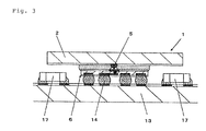
- FIG. 3 is a diagram illustrating such an exemplary embodiment in which semiconductor apparatus 1 according to the first exemplary embodiment of the present invention is installed on a motherboard.
- the shape of semiconductor apparatus 1 is a roughly square plate, and semiconductor apparatus 1 includes semiconductor chip 2 in which a predetermined circuit is formed on main surface 2 a .
- semiconductor apparatus 1 includes a plurality of electrode pads 3 arranged in line on central line 2 d in a main surface 2 a side of semiconductor chip 2 .
- Insulating passivation film 4 is formed on main surface 2 a of semiconductor chip 2 excluding electrode pad 3 , and protects a circuit-formed surface of semiconductor chip 2 .
- a logic circuit such as a microprocessor or a storing circuit such as an SRAM (Static Random Access Memory) and a DRAM (Dynamic Random Access Memory) are formed.
- Bump electrodes 5 for connecting to the wired board that will be mentioned later are formed on a plurality of electrode pads 3 formed on semiconductor chip 2 respectively.
- Bump electrode 5 is, for example, formed on electrode pad 3 by ultrasonic thermal compression-bonding a wire, in which a ball is formed at a melted tip, and by breaking the wire.
- Wired board 6 configured with a smaller area than that of semiconductor chip 2 is allocated in the main surface 2 a side of semiconductor chip 2 .
- Wired board 6 is, for example, a wired board whose shape is a tape, and a plurality of lands 8 for connecting an external terminal that will be mentioned later, and wiring 9 for connecting land 8 and bump electrode 5 formed on electrode pad 3 of semiconductor chip 2 are formed on tape base material 7 made of polyimide resin, and the like.
- Solder resist 10 which is an insulating protection film, is provided on a surface of tape base material 7 excluding the connection part of land 8 , and the like.
- Wired board 6 is mounted in a roughly central area of semiconductor chip 2 with being electrically connected to wiring 9 through bump electrode 5 and conductive material 11 such as solder.
- bump electrodes 5 are arranged in line on central line 2 d
- wired board 6 is formed along a longitudinal direction of semiconductor chip 2 in a rectangle shape.
- Space areas 2 b 1 and 2 c 1 are formed between edge parts 6 b and 6 c of wired board 6 , and edge parts 2 b and 2 c of semiconductor chip 2 .
- the width of space areas 2 b 1 and 2 c 1 is at least 50 ⁇ m or more. In the example illustrated in FIG.
- space area 2 b 1 from edge part 6 b of wired board 6 to edge part 2 b of semiconductor chip 2 is 50 ⁇ m.
- an area surrounded by space areas 2 b , and 2 c 1 on main surface 2 a of semiconductor chip 2 is designated as a central area.
- the present invention can operate a dicing blade, which rotation-grinds so as to dice a semiconductor wafer, and which prevents wired board 6 from being peeled, and the like.
- Chamfer parts 12 are formed at four corners of wired board 6 , and are configured so that it is difficult to peel wired board 6 .
- chamfer parts 12 may be shaped in any cut out shape other than an R chamfer as illustrated in the figure, and may be a C chamfer.
- Wired board 6 may be allocated in an area other than the central area of semiconductor chip 2 .
- Wired board 6 even when a warp is induced in semiconductor chip 2 because of a thermal stress, or the like, it is difficult to influence the central area by the warp, and the reliability can be increased, so that it is preferable to mount wired board 6 in the central area of semiconductor chip 2 .
- wired board 6 Four sides of wired board 6 are allocated within an area of semiconductor chip 2 , and wired board 6 is formed so that an area of wired board 6 is smaller than that of semiconductor chip 2 , so that the number of wired boards 6 to be produced for each shot can be increased, and the stress that is caused by secondary installation of semiconductor apparatus 1 can be also reduced.
- a plurality of external terminals 14 to be installed on motherboard 13 , and the like are allocated in a reticular pattern on land 8 provided on wired board 6 .
- External terminal 14 is formed by mounting a ball made of, for example, solder, and the like on land 8 through a flux, and reflowing.
- the radius side of external terminal 14 is, for example, 0.35 mm, and external terminal 14 is allocated in a 0.5 mm pitch, so that external terminal 14 can be efficiently allocated on wired board 6 .
- External terminals 14 are allocated together on wired board 6 whose area is small, so that wiring 9 on wired board 6 can also be shortened, and electrical characteristics of semiconductor apparatus 1 can be also improved.
- Underfill material 15 is provided as insulating sealing material between semiconductor chip 2 and wired board 6 . While underfill material 15 may be configured so as to cover at least connection part (connection pad) 16 between bump electrode 5 and wiring 9 , in the present exemplary embodiment, since tape-shaped wired board 6 is mounted without bending on semiconductor chip 2 , underfill material 15 is provided so as to cover between semiconductor chip 2 and wired board 6 .
- semiconductor apparatus 1 is configured with semiconductor chip 2 in which a plurality of electrode pads 3 are provided on main surface 2 a , is configured with a plurality of bump electrodes 5 provided on electrode pads 3 of semiconductor chip 2 , is configured with wired board 6 is allocated on the main surface 2 a side of semiconductor chip 2 , and which is positioned in the central area of main surface 2 a of semiconductor chip 2 so as to be separated by at least 50 ⁇ mm or more from edge parts 2 b and 2 c of semiconductor chip 2 , is configured with a plurality of external terminals 14 are provided on wired board 6 , and which are electrically connected to a plurality of bump electrodes 5 through wirings 9 of wired board 6 , and is configured with a sealing part is provided between semiconductor chip 2 and wired board 6 , and which is made of underfill material 15 covering at least the connection part between bump electrode 5 and wiring 9 , thereby, semiconductor apparatus 1 having a real chip size can be realized.
- wired board 6 since the area of wired board 6 is smaller than that of semiconductor chip 2 , the number of wired boards 6 to be manufactured for each shot can be increased, and the cost of semiconductor apparatus 1 can be reduced. In the present invention, by causing the area of wired board 6 to be smaller than that of semiconductor chip 2 , wired boards 6 can be mounted so as to avoid the neighborhood of edge parts 2 b and 2 c of semiconductor chip 2 to which the stress of the secondary installation of semiconductor apparatus 1 is applied, so that the stress applied to semiconductor apparatus 1 can be reduced. In the present invention, since wired board 6 is smaller than semiconductor chip 2 , it also becomes easier to inject underfill material 15 between semiconductor chip 2 and wired boards 6 .
- wired boards 6 By causing wired boards 6 to be configured to be smaller than that of semiconductor chip 2 , the area of part installed to motherboard 13 can be also reduced. In the present invention, since wiring 9 on wired boards 6 can be configured to be short, the electrical characteristics of semiconductor apparatus 1 can be also improved.
- the present invention as described above, by causing the area of wired board 6 to be smaller than that of semiconductor chip 2 , as illustrated in FIG. 3 , the area of the part installed on motherboard 13 can be reduced. Thereby, small-size passive parts 17 such as a chip condenser can be mounted in a free area of motherboard 13 , so that the present invention can contribute to reducing the size of motherboard 13 .
- FIG. 4 is a diagram illustrating a modified example of a connection structure between bump electrode 5 of semiconductor chip 2 and wired board 6 , and each of concavity parts 18 is provided at the position of wired board 6 that corresponds to bump electrode 5 .
- Concavity part 18 is sufficient large so as to allow the extent that bump electrode 5 be positioned in Concavity part 18 .
- a surface layer wiring of the external terminal side of wired board 6 is configured as being exposed, and bump electrode 5 is connected to the surface layer wiring of the external terminal side of wired board 6 through conductive material 11 . Thereby, semiconductor apparatus 1 can be further thinned.
- Plating 19 of Cu/Ni/Au is provided on the surface layer wiring in concavity part 18 , so that semiconductor chip 2 and wired board 6 can be favorably and electrically connected. Since concavity part 18 is provided in an electrical connection part, the bonding area between semiconductor chip 2 and wired board 6 can be enlarged.
- FIG. 5 is a diagram illustrating a modified example of a connection structure when a multilayer wired board is used.
- concavity part 18 is provided at the part of wired board 6 that corresponds to bump electrode 5 , and the multilayer wired board is used so that wiring 9 is exposed in concavity part 18 , thereby, the height of semiconductor apparatus 1 is further suppressed, and wiring 9 can be realized in a high density.
- FIGS. 6 to 8 are diagrams illustrating the production flow of semiconductor apparatus 1 according to the present exemplary embodiment.
- FIGS. 6 to 8 A method of manufacturing semiconductor apparatus 1 according to one exemplary embodiment of the present invention will be described as referring to FIGS. 6 to 8 .
- semiconductor wafer 20 is provided to manufacture semiconductor apparatus 1 , which is, for example, obtained by forming desired circuits and electrode pads through a diffusion process, and the like on the main surface of a disk-like substrate obtained by slicing a silicon ingot formed by a single crystal pulling method, or the like.
- adhesive heat-resistant tape 22 is put around frame-like jig 21 , and the rear surface of semiconductor wafer 20 is placed and fixed on heat-resistant tape 22 .
- a plurality of electrode pads 3 are formed in each of semiconductor chips 2 provided in semiconductor wafer 20 , and as illustrated in FIG. 7A , bump electrode 5 is formed on electrode pad 3 .
- Bump electrode 5 is formed by ultrasonic thermal compression-bonding a wire, in which a ball is formed at a melted tip, on electrode pad 3 , and by breaking the wire. Meanwhile, bump electrode 5 may be formed by the plating, or the like.
- underfill material 15 can be, for example, selectively formed by mounting mask 23 including an aperture in a bump forming area of semiconductor wafer 20 , and pouring underfill material 15 into the aperture with squeegee 24 . Meanwhile, underfill material 15 may be configured to be formed on the whole surface by spinner-applying it to semiconductor wafer 20 . In the spinner-applying, underfill material 15 that has a uniform thickness can be more efficiently formed on semiconductor wafer 20 .
- wired board 6 is previously provided, whose area is smaller than that of semiconductor chip 2 , and in which a plurality of lands 8 , and desired wiring 9 for connecting land 8 and bump electrode 5 formed on electrode pad 3 of semiconductor chip 2 are formed.
- Conductive material 11 such as solder is previously provided in the connection part to bump electrode 5 of wired board 6 .
- wired board 6 is mounted on semiconductor chip 2 by aligning electrode pad 3 of semiconductor chip 2 and connection part (connection pad) 16 of wired board 6 while being absorbed by absorbing collet 25 , or the like, and electrically connecting connection part (connection pad) 16 of wired board 6 and bump electrode 5 through conductive material 11 .
- wired board 6 is mounted on only semiconductor chip 2 which is determined as the non-defective product on semiconductor wafer 20 based on a result of a previous burn-in test and the like. As described above, since wired board 6 is not mounted on semiconductor chip 2 which is determined as a defective product, the process efficiency for mounting wired board 6 can be improved. Since wired board 6 can be efficiently utilized, costs can be also reduced.
- Wired board 6 may be efficiently mount by providing absorbing collet 25 for mounting wired board 6 with a heating mechanism, and by heating wired board 6 in addition to transferring wired board 6 .
- underfill material 15 is expanded, which is the sealing material selectively applied so as to cover electrode pad 3 , and underfill material 15 covers a space between semiconductor chip 2 and wired board 6 .
- underfill material 15 may be formed by injecting insulating underfill material 15 from the space between semiconductor chip 2 and wired board 6 after wired board 6 is mounted on semiconductor chip 2 .
- Semiconductor chip 2 in which wired board 6 is mounted is subjected to a ball mounting process, as illustrated in FIG. 7D , a conductive ball is mounted on land 8 on wired board 6 , and a plurality of external terminals 14 are formed.
- mounting tool 26 in which a plurality of absorbing holes are formed is used by allocating the ball on land 8 on wired board 6 . That is, by using mounting tool 26 , for example, ball 27 made of solder, or the like is held at the absorbing hole, flux is transcription-formed on held ball 27 , and balls 27 are mounted together on land 8 on wired board 6 , thereby, a plurality of external terminals 14 are formed. After ball 27 is mounted, ball 27 is fixed by reflowing, and external terminal 14 is formed on land 8 .
- semiconductor wafer 20 is subjected to a dicing process, and as illustrated in FIG. 7E , semiconductor wafer 20 is cut and separated into each semiconductor chip 2 .
- semiconductor wafer 20 is, for example, placed on a dicing table, and is cut by rotation-grinding dicing line 29 between semiconductor chips 2 by using high rate-rotating dicing blade 28 .
- wired board 6 is mounted so that edge parts 6 b and 6 c thereof are separated from edge parts 2 b and 2 c of semiconductor chip 2 by 50 ⁇ m or more. As described above, by mounting wired board 6 as separated from edge parts 2 b and 2 c of semiconductor chip 2 by 50 ⁇ m or more, it is possible to reduce the peeling of edge parts 6 b and 6 c of wired board 6 when semiconductor wafer 20 is diced.
- semiconductor chip 2 is pushed up from the lower side of heat-resistant tape 22 by pushing up means 30 of a picking-up apparatus, and is removed from heat-resistant tape 22 , and semiconductor chip 2 on which wired board 6 is mounted is picked up.
- semiconductor apparatus 1 of a real chip size as illustrated in FIG. 1 can be obtained.
- semiconductor apparatus 1 is manufactured as a wafer by using wired board 6 whose area is smaller than that of semiconductor chip 2 , semiconductor apparatus 1 can be efficiently manufactured.
- wired board 6 since wired board 6 is used whose area is smaller than that of semiconductor chip 2 , the number of wired boards 6 to be manufactured for each shot can be increased, and the cost of semiconductor apparatus 1 can be reduced.
- wired board 6 since wired board 6 is mounted only on the non-defective chip of semiconductor wafer 20 , wired board 6 can be efficiently mounted.
- semiconductor wafer 20 can be favorably cut without coming into contact with dicing blade 28 when being diced.
- Semiconductor apparatus 1 according to the present exemplary embodiment is structured so that resin and the like are not provided in the cutting area of semiconductor chip 2 , so that it is possible to improve the cutting capability for the dicing, to prevent dicing blade 28 from being worn away due to a filler included in the resin, and the like, and to prevent dicing blade 28 from being consumed.
- FIG. 9 is a side cross-section diagram illustrating the package structure of semiconductor apparatus 1 according to the present exemplary embodiment.
- FIG. 10 is a perspective diagram which is obtained by viewing, from a rear surface side, semiconductor apparatus 1 according to the present exemplary embodiment.
- the shape of semiconductor apparatus 1 is a roughly square plate as in the first exemplary embodiment, and semiconductor apparatus 1 includes semiconductor chip 2 in which a predetermined circuit is formed on main surface 2 a .
- semiconductor apparatus 1 includes a plurality of electrode pads 3 arranged in line on a roughly central area, for example, a central area of main surface 2 a side of semiconductor chip 2 .
- Insulating passivation film 4 is formed on main surface 2 a of semiconductor chip 2 excluding electrode pads 3 , and protects a circuit-formed surface of semiconductor chip 2 .
- bump electrodes 5 for connecting to wired board 6 are formed on a plurality of electrode pads 3 formed on semiconductor chip 2 respectively.
- Wired board 6 whose area is smaller than that of semiconductor chip 2 is allocated in an upper side of main surface 2 a of semiconductor chip 2 .
- Wired board 6 is a wired board whose shape is, for example, a tape, and a plurality of lands 8 for connecting an external terminal that will be mentioned later, and wirings 9 for connecting land 8 and bump electrode 5 formed on electrode pad 3 of semiconductor chip 2 are formed on tape base material 7 made of polyimide resin, and the like.
- An insulating protection film, e.g. solder resist 10 is provided on a surface of tape base material 7 excluding a connection part such as land 8 .
- Wired board 6 is electrically connected to wiring 9 through conductive material 11 to be mounted in the roughly central area of semiconductor chip 2 .
- wired board 6 is formed along a longitudinal direction of semiconductor chip 2 in a rectangle shape.
- Chamfer parts 12 are formed at four corners of wired board 6 , and are configured so that it is difficult to peel wired board 6 .
- the feature of the present exemplary embodiment is, in addition to the features of the first exemplary embodiment, that insulating protection material (first protection material) 31 is provided on the whole surface of an opposite side surface (the other surface) of main surface 2 a of semiconductor chip 2 .
- Epoxy resin, or the like is, for example, used for protection material 31 .
- protection material 31 is formed on the whole back surface of semiconductor wafer 20 in a uniform thickness by spinner-applying liquid resin.
- first protection material 31 made of insulating resin is provided on the other surface side of semiconductor chip 2 , the occurrence of cracks and a chipping in semiconductor chip 2 can be reduced. If first protection material 31 is configured with colored material, as illustrated in FIG. 10 , it becomes possible to clearly display a mark formed in the other surface side of semiconductor chip 2 .
- semiconductor apparatus 1 is configured with semiconductor chip 2 in which a plurality of electrode pads 3 are provided on main surface 2 a , is configured with a plurality of bump electrodes 5 provided on electrode pads 3 of semiconductor chip 2 , is configured with wired board 6 which is allocated on the main surface 2 a side of semiconductor chip 2 , and whose area is smaller than that of semiconductor chip 2 , is configured with a plurality of external terminals 14 which are provided on wired board 6 , and which are electrically connected to a plurality of bump electrodes 5 through wirings 9 of wired board 6 , is configured with sealing material which is provided between semiconductor chip 2 and wired board 6 , and which is made of underfill material 15 covering at least the connection part between bump electrodes 5 and wiring 9 , is configured with first protection material 31 which is provided so as to cover a rear surface of semiconductor chip 2 in a surface side facing main surface 2 a of semiconductor chip 2 , thereby, semiconductor apparatus 1 having a real chip size can be realized, and a chip rear surface can be
- wired board 6 becomes smaller, and the number of wired boards 6 to be manufactured for each shot can be increased, the cost of semiconductor apparatus 1 can be reduced.
- the stress applied to semiconductor chip 2 can be reduced.
- wired board 6 since wired board 6 is small, it also becomes easy to pour underfill material 15 between semiconductor chip 2 and wired boards 6 .
- wired board 6 since wired board 6 is caused to be small, the area of an installation part to motherboard 13 can be also decreased.
- wiring 9 on wired board 6 can be configured to be short, the electrical characteristics of semiconductor apparatus 1 can be also improved.
- semiconductor wafer 20 is provided, in which a desired circuit and electrode pad 3 are formed.
- a main surface i.e. a circuit-formed surface of semiconductor wafer 20 is adhesion-fixed to BG tape 32 .
- the other surface side of semiconductor wafer 20 is grinded according to a back-grinding process, and as illustrated in FIG. 11B , semiconductor wafer 20 is thinned to a thickness around 750 ⁇ m.
- first protection material 31 is formed on the entire other surface of semiconductor wafer 20 .
- First protection material 31 is, for example, formed on a whole surface by spinner-applying insulating resin for the potting.
- First protection material 31 can be formed in a uniform thickness by forming with the spinner-applying.
- FIG. 11D since first protection material 31 is formed on a rear surface of semiconductor wafer 20 , it becomes easy to handle and transfer semiconductor wafer 20 which is thinned in the back-grinding process.
- bump electrode 5 is formed in electrode pad 3 of semiconductor chip 2 , and the sealing material, e.g. underfill material 15 is selectively applied so as to cover bump electrode 5 of semiconductor chip 2 .
- wired board 6 is previously provided, whose area is smaller than that of semiconductor chip 2 , and in which a plurality of lands 8 , and desired wiring 9 for connecting land 8 and bump electrode 5 formed on electrode pad 3 of semiconductor chip 2 are formed.
- wired board 6 is mounted on semiconductor chip 2 .
- the sealing material is expanded, which is selectively applied so as to cover electrode pad 3 , and which covers a space between semiconductor chip 2 and wired board 6 .
- the conductive ball is mounted on land 8 on wired board 6 , and a plurality of external terminals 14 are formed.
- semiconductor wafer 20 is subjected to the dicing process, and semiconductor wafer 20 is cut and separated into each semiconductor chip 2 .
- first protection material 31 which is formed on the rear surface of semiconductor wafer 20 , is also cut and separated.
- the adhesive force is reduced by UV-radiating BG tape 32 .
- the rear surface of semiconductor chip 2 is pushed up from a lower side of BG tape 32 , whose adhesive force is reduced, by pushing up means 30 of a picking-up apparatus, and is removed from BG tape 32 , and semiconductor chip 2 on which wired board 6 is mounted is picked up.
- first protection material 31 is provided on the rear surface of semiconductor chip 2 .
- semiconductor apparatus 1 is manufactured as a wafer by using wired board 6 whose area is smaller than that of semiconductor chip 2 , semiconductor apparatus 1 can be efficiently manufactured. Since wired board 6 , whose area is smaller than that of semiconductor chip 2 , is used, the number of wired boards 6 to be manufactured for each shot can be increased, and the cost of semiconductor apparatus 1 can be reduced.
- Semiconductor apparatus 1 is structured so as not to include resin and the like in a cutting area of semiconductor chip 2 , so that it is possible to improve the cutting capability for dicing, to prevent dicing blade 28 from being worn away due to a filler included in the resin, and the like, and to prevent dicing blade 28 from being consumed.
- FIG. 12 is a cross-section diagram illustrating a package structure of semiconductor apparatus 1 according to the present exemplary embodiment.
- semiconductor apparatus 1 includes second insulating protection material 33 in an area excluding an area in which wired board 6 is mounted on main surface 2 a of semiconductor chip 2 .
- second protection material 33 is formed as surrounding an area in which wired board 6 is mounted, the circuit surface of semiconductor apparatus 1 can be protected. Thereby, the occurrence of cracks and a chipping in semiconductor chip 2 can be prevented.
- FIG. 13 is a cross-section diagram illustrating a modified example of semiconductor apparatus 1 according to the present exemplary embodiment.
- the above sealing material and second protection material 33 are configured to be formed together by spinner-applying the same material.
- underfill material 15 is formed on main surface 2 a of semiconductor wafer 20 by spinner-applying, and wired board 6 is mounted, thereby, it is possible to efficiently form the sealing part and also second protection material 33 .
- the present invention is not limited to the above exemplary embodiments, and a variety of changes and modifications can be applied without departing from the concept of the present invention.
- the present invention can be also applied to the semiconductor chip, as illustrated in FIG. 15 , in which two lines of electrode pads are arranged in the central area, and can also be applied to the semiconductor chip, as illustrated in FIG. 16 , in which the electrode pads are arranged in a cross-shape in the central area.
- the present invention can also be applied to semiconductor apparatus 1 , as illustrated in FIG. 17 , in which the electrode pads are arranged in a peripheral part of the central area.
- the present invention can also be applied to semiconductor apparatus 1 in which wired board 6 and small wired board 6 ′ whose area is smaller than that of wired board 6 are mounted in the central area. Meanwhile, the present invention can be also obviously applied to semiconductor apparatus 1 in which a plurality of small wired boards 6 ′ are mounted.
- the present invention can also be applied to semiconductor apparatus 1 in which a plurality of wired boards 6 are mounted in the central area.
- the present invention can be applied to the semiconductor apparatus in which a wired board such as CSP (Chip Size Package), MCP (Multi Chip Package), and SiP (System in Package) is used.
- CSP Chip Size Package
- MCP Multi Chip Package
- SiP System in Package
Abstract
Description
Claims (21)
Priority Applications (1)
| Application Number | Priority Date | Filing Date | Title |
|---|---|---|---|
| US13/106,333 US8441126B2 (en) | 2007-07-18 | 2011-05-12 | Semiconductor device |
Applications Claiming Priority (2)
| Application Number | Priority Date | Filing Date | Title |
|---|---|---|---|
| JP2007-186895 | 2007-07-18 | ||
| JP2007186895A JP5372346B2 (en) | 2007-07-18 | 2007-07-18 | Semiconductor device and manufacturing method thereof |
Related Child Applications (1)
| Application Number | Title | Priority Date | Filing Date |
|---|---|---|---|
| US13/106,333 Division US8441126B2 (en) | 2007-07-18 | 2011-05-12 | Semiconductor device |
Publications (2)
| Publication Number | Publication Date |
|---|---|
| US20090020873A1 US20090020873A1 (en) | 2009-01-22 |
| US7964962B2 true US7964962B2 (en) | 2011-06-21 |
Family
ID=40264172
Family Applications (2)
| Application Number | Title | Priority Date | Filing Date |
|---|---|---|---|
| US12/173,245 Expired - Fee Related US7964962B2 (en) | 2007-07-18 | 2008-07-15 | Method of manufacturing a semiconductor apparatus |
| US13/106,333 Expired - Fee Related US8441126B2 (en) | 2007-07-18 | 2011-05-12 | Semiconductor device |
Family Applications After (1)
| Application Number | Title | Priority Date | Filing Date |
|---|---|---|---|
| US13/106,333 Expired - Fee Related US8441126B2 (en) | 2007-07-18 | 2011-05-12 | Semiconductor device |
Country Status (5)
| Country | Link |
|---|---|
| US (2) | US7964962B2 (en) |
| JP (1) | JP5372346B2 (en) |
| KR (1) | KR101014577B1 (en) |
| DE (1) | DE102008031511A1 (en) |
| TW (1) | TWI433282B (en) |
Cited By (1)
| Publication number | Priority date | Publication date | Assignee | Title |
|---|---|---|---|---|
| US20090242258A1 (en) * | 2008-03-31 | 2009-10-01 | Fujitsu Limited | Electronic device package with connection terminals including uneven contact surfaces |
Families Citing this family (6)
| Publication number | Priority date | Publication date | Assignee | Title |
|---|---|---|---|---|
| JP5398773B2 (en) * | 2011-04-07 | 2014-01-29 | 富士フイルム株式会社 | Radiation detector |
| KR101974191B1 (en) * | 2012-11-29 | 2019-04-30 | 에스케이하이닉스 주식회사 | Semiconductor device and method for forming the same |
| JP6114181B2 (en) * | 2013-12-27 | 2017-04-12 | 京セラ株式会社 | Manufacturing method of multi-cavity wiring board |
| JP2015128120A (en) * | 2013-12-28 | 2015-07-09 | 京セラサーキットソリューションズ株式会社 | Multi-piece wiring board and manufacturing method of the same |
| KR101598301B1 (en) | 2014-11-28 | 2016-03-14 | 신은수 | Blind |
| CN113496929B (en) * | 2021-07-07 | 2022-06-10 | 哈尔滨宇龙自动化有限公司 | Micro-connection separation device for PLC type optical chip sealing and measuring processing and use method |
Citations (12)
| Publication number | Priority date | Publication date | Assignee | Title |
|---|---|---|---|---|
| WO1999023696A1 (en) | 1997-10-30 | 1999-05-14 | Hitachi, Ltd. | Semiconductor device and method for manufacturing the same______ |
| JP2000003939A (en) | 1999-06-03 | 2000-01-07 | Hitachi Ltd | Semiconductor device adhesive film |
| JP2000106257A (en) | 1998-09-29 | 2000-04-11 | Hitachi Ltd | Socket for inspecting semiconductor element, semiconductor device, manufacture of the semiconductor device, and method for inspecting the semiconductor device |
| US6064114A (en) | 1997-12-01 | 2000-05-16 | Motorola, Inc. | Semiconductor device having a sub-chip-scale package structure and method for forming same |
| US6137185A (en) * | 1996-01-16 | 2000-10-24 | Hitachi, Ltd. | Electrode structure of a wiring substrate of semiconductor device having expanded pitch |
| KR20000068303A (en) | 1997-06-23 | 2000-11-25 | 마치오 나카지마 | Semiconductor package and method for manufacturing the same |
| KR100332863B1 (en) | 1999-09-10 | 2002-04-17 | 이형도 | Printed circuit board with thickness display function |
| KR20020049821A (en) | 2000-12-20 | 2002-06-26 | 박종섭 | chip scale semiconductor package in wafer level and method for fabricating the same |
| JP2004006670A (en) | 2002-02-25 | 2004-01-08 | Seiko Epson Corp | Semiconductor wafer with spacer and manufacturing method thereof, semiconductor device and manufacturing method thereof, circuit board, and electronic apparatus |
| JP2005032820A (en) | 2003-07-08 | 2005-02-03 | Rohm Co Ltd | Method for manufacturing semiconductor device, and semiconductor device |
| US6975035B2 (en) | 2002-03-04 | 2005-12-13 | Micron Technology, Inc. | Method and apparatus for dielectric filling of flip chip on interposer assembly |
| US7314780B2 (en) * | 2002-08-27 | 2008-01-01 | Shinko Electric Industries Co., Ltd. | Semiconductor package, method of production of same, and semiconductor device |
Family Cites Families (5)
| Publication number | Priority date | Publication date | Assignee | Title |
|---|---|---|---|---|
| JP4094074B2 (en) | 1996-03-22 | 2008-06-04 | 株式会社ルネサステクノロジ | Semiconductor integrated circuit device |
| JP2000150713A (en) * | 1998-11-17 | 2000-05-30 | Matsushita Electric Ind Co Ltd | Semiconductor device and its manufacture, and manufacture of electronic part using the same |
| US6214640B1 (en) * | 1999-02-10 | 2001-04-10 | Tessera, Inc. | Method of manufacturing a plurality of semiconductor packages |
| JP3619395B2 (en) * | 1999-07-30 | 2005-02-09 | 京セラ株式会社 | Semiconductor device built-in wiring board and manufacturing method thereof |
| JP2002141444A (en) * | 2000-11-01 | 2002-05-17 | Sony Corp | Semiconductor device and method of manufacturing the same |
-
2007
- 2007-07-18 JP JP2007186895A patent/JP5372346B2/en not_active Expired - Fee Related
-
2008
- 2008-06-25 TW TW097123667A patent/TWI433282B/en not_active IP Right Cessation
- 2008-07-03 DE DE102008031511A patent/DE102008031511A1/en not_active Withdrawn
- 2008-07-15 US US12/173,245 patent/US7964962B2/en not_active Expired - Fee Related
- 2008-07-18 KR KR1020080070279A patent/KR101014577B1/en not_active IP Right Cessation
-
2011
- 2011-05-12 US US13/106,333 patent/US8441126B2/en not_active Expired - Fee Related
Patent Citations (12)
| Publication number | Priority date | Publication date | Assignee | Title |
|---|---|---|---|---|
| US6137185A (en) * | 1996-01-16 | 2000-10-24 | Hitachi, Ltd. | Electrode structure of a wiring substrate of semiconductor device having expanded pitch |
| KR20000068303A (en) | 1997-06-23 | 2000-11-25 | 마치오 나카지마 | Semiconductor package and method for manufacturing the same |
| WO1999023696A1 (en) | 1997-10-30 | 1999-05-14 | Hitachi, Ltd. | Semiconductor device and method for manufacturing the same______ |
| US6064114A (en) | 1997-12-01 | 2000-05-16 | Motorola, Inc. | Semiconductor device having a sub-chip-scale package structure and method for forming same |
| JP2000106257A (en) | 1998-09-29 | 2000-04-11 | Hitachi Ltd | Socket for inspecting semiconductor element, semiconductor device, manufacture of the semiconductor device, and method for inspecting the semiconductor device |
| JP2000003939A (en) | 1999-06-03 | 2000-01-07 | Hitachi Ltd | Semiconductor device adhesive film |
| KR100332863B1 (en) | 1999-09-10 | 2002-04-17 | 이형도 | Printed circuit board with thickness display function |
| KR20020049821A (en) | 2000-12-20 | 2002-06-26 | 박종섭 | chip scale semiconductor package in wafer level and method for fabricating the same |
| JP2004006670A (en) | 2002-02-25 | 2004-01-08 | Seiko Epson Corp | Semiconductor wafer with spacer and manufacturing method thereof, semiconductor device and manufacturing method thereof, circuit board, and electronic apparatus |
| US6975035B2 (en) | 2002-03-04 | 2005-12-13 | Micron Technology, Inc. | Method and apparatus for dielectric filling of flip chip on interposer assembly |
| US7314780B2 (en) * | 2002-08-27 | 2008-01-01 | Shinko Electric Industries Co., Ltd. | Semiconductor package, method of production of same, and semiconductor device |
| JP2005032820A (en) | 2003-07-08 | 2005-02-03 | Rohm Co Ltd | Method for manufacturing semiconductor device, and semiconductor device |
Non-Patent Citations (2)
| Title |
|---|
| German Office Action and its English translation of Oct. 18, 2010 in corresponding German Serial No. 10 2008 031 511.7-33. |
| KR Office Action dated Jul. 1, 2010 (English translation attached). |
Cited By (2)
| Publication number | Priority date | Publication date | Assignee | Title |
|---|---|---|---|---|
| US20090242258A1 (en) * | 2008-03-31 | 2009-10-01 | Fujitsu Limited | Electronic device package with connection terminals including uneven contact surfaces |
| US8264850B2 (en) * | 2008-03-31 | 2012-09-11 | Fujitsu Limited | Electronic device package with connection terminals including uneven contact surfaces |
Also Published As
| Publication number | Publication date |
|---|---|
| JP5372346B2 (en) | 2013-12-18 |
| TWI433282B (en) | 2014-04-01 |
| DE102008031511A1 (en) | 2009-04-23 |
| JP2009026860A (en) | 2009-02-05 |
| KR101014577B1 (en) | 2011-02-16 |
| US8441126B2 (en) | 2013-05-14 |
| TW200905827A (en) | 2009-02-01 |
| US20090020873A1 (en) | 2009-01-22 |
| US20120119356A1 (en) | 2012-05-17 |
| KR20090009164A (en) | 2009-01-22 |
Similar Documents
| Publication | Publication Date | Title |
|---|---|---|
| US8076770B2 (en) | Semiconductor device including a first land on the wiring substrate and a second land on the sealing portion | |
| US6737300B2 (en) | Chip scale package and manufacturing method | |
| US8575763B2 (en) | Semiconductor device and method of manufacturing the same | |
| US8441126B2 (en) | Semiconductor device | |
| US8426983B2 (en) | Semiconductor device | |
| US7667473B1 (en) | Flip-chip package having thermal expansion posts | |
| US20100148172A1 (en) | Semiconductor device | |
| JP2009212315A (en) | Semiconductor device and manufacturing method thereof | |
| US20190157209A1 (en) | Chip package and manufacturing method thereof | |
| US20120146242A1 (en) | Semiconductor device and method of fabricating the same | |
| US6911737B2 (en) | Semiconductor device package and method | |
| US6953709B2 (en) | Semiconductor device and its manufacturing method | |
| US7786564B2 (en) | Semiconductor device and method for manufacturing semiconductor device | |
| EP2543066B1 (en) | Thermal vias in an integrated circuit package with an embedded die | |
| US6455941B1 (en) | Chip scale package | |
| JP2010010269A (en) | Semiconductor device, intermediate for manufacturing semiconductor device, and method of manufacturing them | |
| US20100301468A1 (en) | Semiconductor device and method of manufacturing the same | |
| US20060284301A1 (en) | CSP semiconductor chip and BGA assembly with enhanced physical protection, protective members and assemblies used with same, and methods of enhancing physical protection of chips and assemblies | |
| US6266249B1 (en) | Semiconductor flip chip ball grid array package | |
| JP3339472B2 (en) | Semiconductor device and manufacturing method thereof | |
| US8878070B2 (en) | Wiring board and method of manufacturing a semiconductor device | |
| US7812439B2 (en) | Semiconductor package with reduced length interconnect and manufacturing method thereof | |
| JP2007142128A (en) | Semiconductor device and its production process | |
| CN117524993A (en) | Electronic package and method for manufacturing the same | |
| KR100753795B1 (en) | Semiconductor package and manufacturing method the same |
Legal Events
| Date | Code | Title | Description |
|---|---|---|---|
| AS | Assignment |
Owner name: ELPIDA MEMORY, INC., JAPAN Free format text: ASSIGNMENT OF ASSIGNORS INTEREST;ASSIGNORS:WATANABE, MITSUHISA;ANJOH, ICHIRO;REEL/FRAME:021238/0072 Effective date: 20080609 |
|
| FEPP | Fee payment procedure |
Free format text: PAYOR NUMBER ASSIGNED (ORIGINAL EVENT CODE: ASPN); ENTITY STATUS OF PATENT OWNER: LARGE ENTITY |
|
| STCF | Information on status: patent grant |
Free format text: PATENTED CASE |
|
| AS | Assignment |
Owner name: ELPIDA MEMORY INC., JAPAN Free format text: SECURITY AGREEMENT;ASSIGNOR:PS4 LUXCO S.A.R.L.;REEL/FRAME:032414/0261 Effective date: 20130726 |
|
| AS | Assignment |
Owner name: PS4 LUXCO S.A.R.L., LUXEMBOURG Free format text: ASSIGNMENT OF ASSIGNORS INTEREST;ASSIGNOR:ELPIDA MEMORY, INC.;REEL/FRAME:032900/0568 Effective date: 20130726 |
|
| FPAY | Fee payment |
Year of fee payment: 4 |
|
| AS | Assignment |
Owner name: PS5 LUXCO S.A.R.L., LUXEMBOURG Free format text: ASSIGNMENT OF ASSIGNORS INTEREST;ASSIGNOR:PS4 LUXCO S.A.R.L.;REEL/FRAME:039818/0506 Effective date: 20130829 Owner name: LONGITUDE SEMICONDUCTOR S.A.R.L., LUXEMBOURG Free format text: CHANGE OF NAME;ASSIGNOR:PS5 LUXCO S.A.R.L.;REEL/FRAME:039793/0880 Effective date: 20131112 |
|
| AS | Assignment |
Owner name: LONGITUDE LICENSING LIMITED, IRELAND Free format text: ASSIGNMENT OF ASSIGNORS INTEREST;ASSIGNOR:LONGITUDE SEMICONDUCTOR S.A.R.L.;REEL/FRAME:046867/0248 Effective date: 20180731 |
|
| FEPP | Fee payment procedure |
Free format text: MAINTENANCE FEE REMINDER MAILED (ORIGINAL EVENT CODE: REM.); ENTITY STATUS OF PATENT OWNER: LARGE ENTITY |
|
| LAPS | Lapse for failure to pay maintenance fees |
Free format text: PATENT EXPIRED FOR FAILURE TO PAY MAINTENANCE FEES (ORIGINAL EVENT CODE: EXP.); ENTITY STATUS OF PATENT OWNER: LARGE ENTITY |
|
| STCH | Information on status: patent discontinuation |
Free format text: PATENT EXPIRED DUE TO NONPAYMENT OF MAINTENANCE FEES UNDER 37 CFR 1.362 |
|
| FP | Lapsed due to failure to pay maintenance fee |
Effective date: 20190621 |