US7972756B2 - Ketal containing photoconductors - Google Patents
Ketal containing photoconductors Download PDFInfo
- Publication number
- US7972756B2 US7972756B2 US11/961,462 US96146207A US7972756B2 US 7972756 B2 US7972756 B2 US 7972756B2 US 96146207 A US96146207 A US 96146207A US 7972756 B2 US7972756 B2 US 7972756B2
- Authority
- US
- United States
- Prior art keywords
- photoconductor
- charge transport
- accordance
- layer
- transport layer
- Prior art date
- Legal status (The legal status is an assumption and is not a legal conclusion. Google has not performed a legal analysis and makes no representation as to the accuracy of the status listed.)
- Expired - Fee Related, expires
Links
Classifications
-
- G—PHYSICS
- G03—PHOTOGRAPHY; CINEMATOGRAPHY; ANALOGOUS TECHNIQUES USING WAVES OTHER THAN OPTICAL WAVES; ELECTROGRAPHY; HOLOGRAPHY
- G03G—ELECTROGRAPHY; ELECTROPHOTOGRAPHY; MAGNETOGRAPHY
- G03G5/00—Recording members for original recording by exposure, e.g. to light, to heat, to electrons; Manufacture thereof; Selection of materials therefor
- G03G5/02—Charge-receiving layers
- G03G5/04—Photoconductive layers; Charge-generation layers or charge-transporting layers; Additives therefor; Binders therefor
- G03G5/05—Organic bonding materials; Methods for coating a substrate with a photoconductive layer; Inert supplements for use in photoconductive layers
- G03G5/0528—Macromolecular bonding materials
- G03G5/0557—Macromolecular bonding materials obtained otherwise than by reactions only involving carbon-to-carbon unsatured bonds
- G03G5/0567—Other polycondensates comprising oxygen atoms in the main chain; Phenol resins
-
- G—PHYSICS
- G03—PHOTOGRAPHY; CINEMATOGRAPHY; ANALOGOUS TECHNIQUES USING WAVES OTHER THAN OPTICAL WAVES; ELECTROGRAPHY; HOLOGRAPHY
- G03G—ELECTROGRAPHY; ELECTROPHOTOGRAPHY; MAGNETOGRAPHY
- G03G5/00—Recording members for original recording by exposure, e.g. to light, to heat, to electrons; Manufacture thereof; Selection of materials therefor
- G03G5/02—Charge-receiving layers
- G03G5/04—Photoconductive layers; Charge-generation layers or charge-transporting layers; Additives therefor; Binders therefor
- G03G5/06—Photoconductive layers; Charge-generation layers or charge-transporting layers; Additives therefor; Binders therefor characterised by the photoconductive material being organic
- G03G5/0601—Acyclic or carbocyclic compounds
- G03G5/0609—Acyclic or carbocyclic compounds containing oxygen
-
- G—PHYSICS
- G03—PHOTOGRAPHY; CINEMATOGRAPHY; ANALOGOUS TECHNIQUES USING WAVES OTHER THAN OPTICAL WAVES; ELECTROGRAPHY; HOLOGRAPHY
- G03G—ELECTROGRAPHY; ELECTROPHOTOGRAPHY; MAGNETOGRAPHY
- G03G5/00—Recording members for original recording by exposure, e.g. to light, to heat, to electrons; Manufacture thereof; Selection of materials therefor
- G03G5/14—Inert intermediate or cover layers for charge-receiving layers
- G03G5/147—Cover layers
- G03G5/14708—Cover layers comprising organic material
- G03G5/14713—Macromolecular material
- G03G5/14747—Macromolecular material obtained otherwise than by reactions only involving carbon-to-carbon unsaturated bonds
- G03G5/1476—Other polycondensates comprising oxygen atoms in the main chain; Phenol resins
Definitions
- photoconductors comprising a photogenerating layer and a charge transport layer, and wherein the photogenerating layer contains a titanyl phthalocyanine prepared by dissolving a Type I titanyl phthalocyanine in a solution comprising a trihaloacetic acid and an alkylene halide; adding the mixture comprising the dissolved Type I titanyl phthalocyanine to a solution comprising an alcohol and an alkylene halide thereby precipitating a Type Y titanyl phthalocyanine; and treating the Type Y titanyl phthalocyanine with a monohalobenzene.
- a titanyl phthalocyanine prepared by dissolving a Type I titanyl phthalocyanine in a solution comprising a trihaloacetic acid and an alkylene halide
- High photosensitivity titanyl phthalocyanines are illustrated in copending U.S. application Ser. No. 10/992,500, U.S. Publication No. 20060105254, the disclosures of which are totally incorporated herein by reference, which, for example, discloses a process for the preparation of a Type V titanyl phthalocyanine, comprising providing a Type I titanyl phthalocyanine; dissolving the Type I titanyl phthalocyanine in a solution comprising a trihaloacetic acid and an alkylene halide like methylene chloride; adding the resulting mixture comprising the dissolved Type I titanyl phthalocyanine to a solution comprising an alcohol and an alkylene halide thereby precipitating a Type Y titanyl phthalocyanine; and treating the Type Y titanyl phthalocyanine with monochlorobenzene to yield a Type V titanyl phthalocyanine.
- a number of the components of the above cross referenced applications such as the supporting substrates, resin binders, antioxidants, charge transport components, photogenerating pigments like hydroxygallium phthalocyanines, and titanyl phthalocyanines, high photosensitivity titanyl phthalocyanines, such as Type V, hole blocking layer components, adhesive layers, and the like, may be selected for the photoconductor and imaging members of the present disclosure in embodiments thereof.
- This disclosure is generally directed to photoconductors and imaging and printing processes thereof. More specifically, the present disclosure is directed to drum, to multilayered drum, and flexible belt photoconductors, or devices comprised of a supporting medium like a substrate, a photogenerating layer, and a charge transport layer, including a plurality of charge transport layers, such as a first charge transport layer and a second charge transport layer, and wherein the first and/or second charge transport layer in contact with the photogenerating layer contains a photoinitiator like a ketal, an ⁇ -hydroxyketone, an ⁇ -diketone, a phosphine oxide, an ⁇ -aminoketone, a triazine, a benzophenone, and mixtures thereof.
- a photoinitiator like a ketal, an ⁇ -hydroxyketone, an ⁇ -diketone, a phosphine oxide, an ⁇ -aminoketone, a triazine, a benzophenone, and mixtures thereof.
- a photoconductor with a photogenerating layer, and a charge transport layer containing a ketal of at least one of a dialkoxy aryl acetophenone, and a hydroxyl(hydroxymethoxy)aryl-alkylpropanone.
- a toner composition comprised, for example, of thermoplastic resin, colorant, such as pigment, charge additive, and surface additive
- the imaging method involves the same operation with the exception that exposure can be accomplished with a laser device or image bar.
- the flexible photoconductor belts disclosed herein can be selected for the Xerox Corporation iGEN® machines that generate with some versions over 100 copies per minute.
- Processes of imaging, especially xerographic imaging and printing, including digital, and/or color printing, are thus encompassed by the present disclosure.
- the imaging members are in embodiments sensitive in the wavelength region of, for example, from about 400 to about 900 nanometers, and in particular from about 650 to about 850 nanometers, thus diode lasers can be selected as the light source.
- the imaging members of this disclosure are useful in color xerographic applications, particularly high-speed color copying and printing processes.
- the photoconductors disclosed may enable, for example, undesirable light shock reductions; the minimization or substantially elimination of undesirable ghosting on developed images, such as xerographic images, including improved ghosting at various relative humidity; excellent cyclic and stable electrical properties; acceptable imaging depletion by, for example, generating free radicals which neutralize excess charge, and dark decay characteristics; minimal charge deficient spots (CDS); and compatibility with the photogenerating and charge transport resin binders.
- Light shock of photoconductor fatigue usually causes dark bands in the resulting xerographic prints from the light exposed photoconductor area at time zero, while the photoconductors disclosed herein in embodiments minimize or avoid this disadvantage in that, for example, the light shock resistant photoconductors do not usually print undesirable dark bands even the photoconductor is exposed to light.
- At least one in embodiments refers, for example, to one, to from 1 to about 10, to from 2 to about 7; to from 2 to about 4; to 2, and the like.
- a photoconductive imaging member comprised of a supporting substrate, a hole blocking layer thereover, a crosslinked photogenerating layer and a charge transport layer, and wherein the photogenerating layer is comprised of a photogenerating component, and a vinyl chloride, allyl glycidyl ether, hydroxy containing polymer.
- a photoconductive imaging member comprised of a hole blocking layer, a photogenerating layer, and a charge transport layer, and wherein the hole blocking layer is comprised of a metal oxide; and a mixture of a phenolic compound and a phenolic resin wherein the phenolic compound contains at least two phenolic groups.
- Layered photoresponsive imaging members have been described in numerous U.S. patents, such as U.S. Pat. No. 4,265,990 wherein there is illustrated an imaging member comprised of a photogenerating layer, and an aryl amine hole transport layer.
- Examples of disclosed photogenerating layer components include trigonal selenium, metal phthalocyanines, vanadyl phthalocyanines, and metal free phthalocyanines.
- Type V hydroxygallium phthalocyanine Illustrated in U.S. Pat. No. 5,521,306, the disclosure of which is totally incorporated herein by reference, is a process for the preparation of Type V hydroxygallium phthalocyanine comprising the in situ formation of an alkoxy-bridged gallium phthalocyanine dimer, hydrolyzing the dimer to hydroxygallium phthalocyanine, and subsequently converting the hydroxygallium phthalocyanine product to Type V hydroxygallium phthalocyanine.
- a process for the preparation of hydroxygallium phthalocyanine photogenerating pigments which comprises hydrolyzing a gallium phthalocyanine precursor pigment by dissolving the hydroxygallium phthalocyanine in a strong acid, and then reprecipitating the resulting dissolved pigment in basic aqueous media; removing any ionic species formed by washing with water, concentrating the resulting aqueous slurry comprised of water and hydroxygallium phthalocyanine to a wet cake; removing water from said slurry by azeotropic distillation with an organic solvent, and subjecting said resulting pigment slurry to mixing with the addition of a second solvent to cause the formation of said hydroxygallium phthalocyanine polymorphs.
- a layered imaging member with, for example, a perylene, pigment photogenerating component and an aryl amine component, such as N,N′-diphenyl-N,N′-bis(3-methylphenyl)-1,1′-biphenyl-4,4′-diamine dispersed in a polycarbonate binder as a hole transport layer.
- aryl amine component such as N,N′-diphenyl-N,N′-bis(3-methylphenyl)-1,1′-biphenyl-4,4′-diamine dispersed in a polycarbonate binder as a hole transport layer.
- Kanemitsu and Funada J. Phys. D: Appl. Phys. 24, 1991, 1409-1415 have apparently suggested that light-induced fatigue of the photoconductor is a consequence of the build-up of the negative charges caused by electron trapping in the photogenerating layer and the positive charges caused by hole trapping at the photogenerating layer charge transport layer interface.
- the photoconductors illustrated herein in embodiments, and with an additive, such as a triazine, and those additives illustrated in the appropriate copending applications filed concurrently herewith, in the charge transport layer results in reduced light shock characteristics as compared to a similar photoconductor with no charge transport layer (CTL) additive as the additive is believed to absorb the UV portion of the white light and generate active species such as free radicals that can interact with or neutralize those light (usually visible light) generated charges within the photoconductor.
- CTL charge transport layer
- the appropriate components such as the supporting substrates, the photogenerating layer components, the charge transport layer components, and the like of the above-recited patents, may be selected for the photoconductors of the present disclosure in embodiments thereof.
- aspects of the present disclosure are directed to a photoconductor comprising a supporting substrate, a photogenerating layer, and at least one charge transport layer comprised of at least one charge transport component, and wherein the at least one charge transport layer contains at least one ketal, or at least one suitable ketone; a photoconductor comprised in sequence of an optional supporting substrate, a photogenerating layer, and a charge transport layer; and wherein the charge transport layer contains a ketal, a benzil ketal, and the like component present in an amount of from about 0.05 to about 15 weight percent; and a photoconductor comprising a supporting substrate, a photogenerating layer, and a hole transport layer; and wherein the hole transport layer has incorporated therein a benzil ketal as represented by or encompassed by at least one of
- R 1 , R 2 , R 3 , and R 4 are each independently at least one of hydrogen, alkyl, and aryl.
- additives such as photoinitiators included in at least one of the charge transport layers of the photoconductor include known ketals, ⁇ -hydroxyketone, ⁇ -diketone, phosphine oxide, ⁇ -aminoketone photoinitiators used in UV curing processes, and the like. While not being desired to be limited by theory, it is believed that upon UV exposure activated species, such as free radicals, are generated by a unimolecular reaction, mainly bond breakage within the photoinitiator molecule itself, and the UV-generated active species from the photoinitiator interacts with or neutralizes that light, usually visible light, generated charges within the photoconductor, resulting in improved light shock resistance.
- activated species such as free radicals
- a number of commercially available photoinitiators that can be selected are ESACURE® available from Lamberti Chemical Specialties, Gallarate, Italy, IRGACURE® and DAROCUR® available from Ciba Specialty Chemicals, Basel, Switzerland, FIRSTCURE® available from Albemarle Corporation, Baton Rouge, La., and LUCIRIN® available from BASF, Ludwigshafen, Germany.
- Ketal examples present in various suitable amounts include those represented by the following formulas/structures
- each R substituent is, for example, hydrogen, alkyl, aryl, substituted alkyl, substituted aryl, and the like:
- Alkyl includes, for example, those groups with from 1 to about 25, from 1 to about 18, from 1 to about 10, or from 1 to about 6 carbon atoms, such as methyl, ethyl, propyl, butyl, pentyl, hexyl, octyl, stearyl, and the like.
- Aryl refers, for example, to those groups that contain from 6 to about 42 carbon atoms, such as phenyl, anthryl, naphthyl, and the like.
- ketal additive examples include ⁇ , ⁇ -dimethoxy- ⁇ -phenylacetophenone (ESACURE® KB1, IRGACURE® 651 and FIRSTCURE® BDK), 2,2-diethoxy acetophenone (FIRSTCURE® DEAP), benzoin ethyl ether, benzoin isobutyl ether, benzoin methyl ether, respectively, represented by the following formulas/structures
- Alpha-hydroxyketone examples present in the charge transport layer in various suitable amounts include those represented by the following formula/structure
- each R substituent is hydrogen, alkyl, aryl, substituted derivatives thereof, and the like as illustrated herein.
- Alpha-diketone examples present in the charge transport layer in various suitable amounts include those represented by the following formula/structure
- each R substituent is hydrogen, alkyl, aryl, substituted derivatives thereof, and the like.
- ⁇ -diketone examples include benzil, camphorquinone, 4,4′-dimethylbenzil, methylbenzoylformate, phenanthrenequinone, respectively, represented by the following formulas/structures
- the thickness of the photoconductor substrate layer depends on various factors, including economical considerations, desired electrical characteristics, adequate flexibility, and the like, thus this layer may be of substantial thickness, for example over 3,000 microns, such as from about 1,000 to about 2,000 microns, from about 500 to about 1,000 microns, or from about 300 to about 700 microns (“about” throughout includes all values in between the values recited), or of a minimum thickness. In embodiments, the thickness of this layer is from about 75 microns to about 300 microns, or from about 100 to about 150 microns.
- the photoconductor can be free of a substrate, for example a layer usually in contact with the substrate can be increased in thickness.
- the substrate or supporting medium may be of a substantial thickness of, for example, up to several centimeters or of a minimum thickness of less than a millimeter.
- a flexible belt may be of a substantial thickness of, for example, about 250 micrometers, or of a minimum thickness of less than about 50 micrometers, provided there are no adverse effects on the final electrophotographic device.
- the photoconductor may in embodiments include a blocking layer, an adhesive layer, a top overcoating protective layer, and an anticurl backing layer.
- the photoconductor substrate may be opaque, substantially opaque, or substantially transparent, and may comprise any suitable material that, for example, permits the photoconductor layers to be supported. Accordingly, the substrate may comprise a number of known layers, and more specifically, the substrate can be comprised of an electrically nonconductive or conductive material such as an inorganic or an organic composition. As electrically nonconducting materials, there may be selected various resins known for this purpose including polyesters, polycarbonates, polyamides, polyurethanes, and the like, which are flexible as thin webs.
- An electrically conducting substrate may comprise any suitable metal of, for example, aluminum, nickel, steel, copper, and the like, or a polymeric material filled with an electrically conducting substance, such as carbon, metallic powder, and the like, or an organic electrically conducting material.
- the electrically insulating or conductive substrate may be in the form of an endless flexible belt, a web, a rigid cylinder, a sheet, and the like.
- the surface thereof may be rendered electrically conductive by an electrically conductive coating.
- the conductive coating may vary in thickness depending upon the optical transparency, degree of flexibility desired, and economic factors, and in embodiments this layer can be of a thickness of from about 0.05 micron to about 5 microns.
- substrates are as illustrated herein, and more specifically, supporting substrate layers selected for the photoconductors of the present disclosure comprise a layer of insulating material including inorganic or organic polymeric materials, such as MYLAR® a commercially available polymer, MYLAR® containing titanium, a layer of an organic or inorganic material having a semiconductive surface layer, such as indium tin oxide, or aluminum arranged thereon, or a conductive material inclusive of aluminum, chromium, nickel, brass, or the like.
- the substrate may be flexible, seamless, or rigid, and may have a number of many different configurations, such as for example, a plate, a cylindrical drum, a scroll, an endless flexible belt, and the like.
- the substrate is in the form of a seamless flexible belt.
- an anticurl layer such as for example polycarbonate materials commercially available as MAKROLON®.
- the photogenerating layer can contain known photogenerating pigments, such as metal phthalocyanines, metal free phthalocyanines, and more specifically, alkylhydroxyl gallium phthalocyanines, hydroxygallium phthalocyanines, chlorogallium phthalocyanines, perylenes, especially bis(benzimidazo)perylene, titanyl phthalocyanines, and the like, and yet more specifically, vanadyl phthalocyanines, Type V hydroxygallium phthalocyanines, and inorganic components such as selenium, selenium alloys, and trigonal selenium.
- metal phthalocyanines such as metal phthalocyanines, metal free phthalocyanines, and more specifically, alkylhydroxyl gallium phthalocyanines, hydroxygallium phthalocyanines, chlorogallium phthalocyanines, perylenes, especially bis(benzimidazo)perylene, titanyl phthalocyanines, and the like
- the photogenerating pigment can be dispersed in a resin binder similar to the resin binders selected for the charge transport layer, or alternatively no resin binder need be present.
- the thickness of the photogenerating layer depends on a number of factors, including the thicknesses of the other layers and the amount of photogenerating material contained in the photogenerating layer. Accordingly, this layer can be of a thickness of, for example, from about 0.05 micron to about 10 microns, and more specifically, from about 0.25 micron to about 2 microns when, for example, the photogenerating compositions are present in an amount of from about 30 to about 75 percent by volume.
- the photogenerating component or pigment is present in a resinous binder in various amounts, inclusive of 100 percent by weight based on the weight of the photogenerating components that are present. Generally, however, from about 5 percent by volume to about 95 percent by volume of the photogenerating pigment is dispersed in about 95 percent by volume to about 5 percent by volume of the resinous binder, or from about 20 percent by volume to about 30 percent by volume of the photogenerating pigment is dispersed in about 70 percent by volume to about 80 percent by volume of the resinous binder composition.
- about 90 percent by volume of the photogenerating pigment is dispersed in about 10 percent by volume of the resinous binder composition, and which resin may be selected from a number of known polymers, such as poly(vinyl butyral), poly(vinyl carbazole), polyesters, polycarbonates, poly(vinyl chloride), polyacrylates and methacrylates, copolymers of vinyl chloride and vinyl acetate, phenolic resins, polyurethanes, poly(vinyl alcohol), polyacrylonitrile, polystyrene, and the like. It is desirable to select a coating solvent that does not substantially disturb or adversely affect the other previously coated layers of the device.
- coating solvents for the photogenerating layer are ketones, alcohols, aromatic hydrocarbons, halogenated aliphatic hydrocarbons, ethers, amines, amides, esters, and the like.
- Specific solvent examples are cyclohexanone, acetone, methyl ethyl ketone, methanol, ethanol, butanol, amyl alcohol, toluene, xylene, chlorobenzene, carbon tetrachloride, chloroform, methylene chloride, trichloroethylene, tetrahydrofuran, dioxane, diethyl ether, dimethyl formamide, dimethyl acetamide, butyl acetate, ethyl acetate, methoxyethyl acetate, and the like.
- examples of polymeric binder materials that can be selected as the matrix for the photogenerating layer components include thermoplastic and thermosetting resins, such as polycarbonates, polyesters, polyamides, polyurethanes, polystyrenes, polyarylethers, polyarylsulfones, polybutadienes, polysulfones, polyethersulfones, polyethylenes, polypropylenes, polyimides, polymethylpentenes, poly(phenylene sulfides), poly(vinyl acetate), polysiloxanes, polyacrylates, polyvinyl acetals, polyamides, polyimides, amino resins, phenylene oxide resins, terephthalic acid resins, phenoxy resins, epoxy resins, phenolic resins, polystyrene, and acrylonitrile copolymers, poly(vinyl chloride), vinyl chloride and vinyl acetate copolymers, acrylate copolymers, alkyd resin
- the photogenerating layer may be fabricated in a dot or line pattern. Removal of the solvent of a solvent-coated layer may be effected by any known conventional techniques such as oven drying, infrared radiation drying, air drying, and the like.
- the final dry thickness of the photogenerating layer is as illustrated herein, and can be, for example, from about 0.01 to about 30 microns after being dried at, for example, about 40° C. to about 150° C. for about 15 to about 90 minutes. More specifically, a photogenerating layer of a thickness, for example, of from about 0.1 to about 30, or from about 0.5 to about 2 microns can be applied to or deposited on the substrate, on other surfaces in between the substrate and the charge transport layer, and the like. A charge blocking layer or hole blocking layer may optionally be applied to the electrically conductive surface prior to the application of a photogenerating layer. When desired, an adhesive layer may be included between the charge blocking or hole blocking layer or interfacial layer and the photogenerating layer. Usually, the photogenerating layer is applied onto the blocking layer and a charge transport layer or plurality of charge transport layers are formed on the photogenerating layer. This structure may have the photogenerating layer on top of or below the charge transport layer.
- a suitable known adhesive layer can be included in the photoconductor.
- Typical adhesive layer materials include, for example, polyesters, polyurethanes, and the like.
- the adhesive layer thickness can vary and in embodiments is, for example, from about 0.05 micrometer (500 Angstroms) to about 0.3 micrometer (3,000 Angstroms).
- the adhesive layer can be deposited on the hole blocking layer by spraying, dip coating, roll coating, wire wound rod coating, gravure coating, Bird applicator coating, and the like. Drying of the deposited coating may be effected by, for example, oven drying, infrared radiation drying, air drying, and the like.
- an adhesive layer usually in contact with or situated between the hole blocking layer and the photogenerating layer, there can be selected various known substances inclusive of copolyesters, polyamides, poly(vinyl butyral), poly(vinyl alcohol), polyurethane, and polyacrylonitrile.
- This layer is, for example, of a thickness of from about 0.001 micron to about 1 micron, or from about 0.1 to about 0.5 micron.
- this layer may contain effective suitable amounts, for example from about 1 to about 10 weight percent, of conductive and nonconductive particles, such as zinc oxide, titanium dioxide, silicon nitride, carbon black, and the like, to provide, for example, in embodiments of the present disclosure further desirable electrical and optical properties.
- the optional hole blocking or undercoat layer or layers for the imaging members of the present disclosure can contain a number of components including known hole blocking components, such as amino silanes, doped metal oxides, a metal oxide like titanium, chromium, zinc, tin and the like; a mixture of phenolic compounds and a phenolic resin, or a mixture of two phenolic resins, and optionally a dopant such as SiO 2 .
- known hole blocking components such as amino silanes, doped metal oxides, a metal oxide like titanium, chromium, zinc, tin and the like
- a mixture of phenolic compounds and a phenolic resin such as a mixture of two phenolic resins
- optionally a dopant such as SiO 2 .
- the phenolic compounds usually contain at least two phenol groups, such as bisphenol A (4,4′-isopropylidenediphenol), E (4,4′-ethylidenebisphenol), F (bis(4-hydroxyphenyl)methane), M (4,4′-(1,3-phenylenediisopropylidene)bisphenol), P (4,4′-(1,4-phenylene diisopropylidene)bisphenol), S (4,4′-sulfonyldiphenol), and Z (4,4′-cyclohexylidenebisphenol); hexafluorobisphenol A (4,4′-(hexafluoro isopropylidene)diphenol), resorcinol, hydroxyquinone, catechin, and the like.
- phenol groups such as bisphenol A (4,4′-isopropylidenediphenol), E (4,4′-ethylidenebisphenol), F (bis(4-hydroxyphenyl)methan
- the hole blocking layer can be, for example, comprised of from about 20 weight percent to about 80 weight percent, and more specifically, from about 55 weight percent to about 65 weight percent of a suitable component like a metal oxide, such as TiO 2 , from about 20 weight percent to about 70 weight percent, and more specifically, from about 25 weight percent to about 50 weight percent of a phenolic resin; from about 2 weight percent to about 20 weight percent, and more specifically, from about 5 weight percent to about 15 weight percent of a phenolic compound preferably containing at least two phenolic groups, such as bisphenol S, and from about 2 weight percent to about 15 weight percent, and more specifically, from about 4 weight percent to about 10 weight percent of a plywood suppression dopant, such as SiO 2 .
- a suitable component like a metal oxide, such as TiO 2
- TiO 2 titanium oxide
- a phenolic resin from about 2 weight percent to about 20 weight percent, and more specifically, from about 5 weight percent to about 15 weight percent of a phenolic compound preferably containing at least two phenol
- the hole blocking layer coating dispersion can, for example, be prepared as follows.
- the metal oxide/phenolic resin dispersion is first prepared by ball milling or dynomilling until the median particle size of the metal oxide in the dispersion is less than about 10 nanometers, for example from about 5 to about 9.
- a phenolic compound and dopant followed by mixing.
- the hole blocking layer coating dispersion can be applied by dip coating or web coating, and the layer can be thermally cured after coating.
- the hole blocking layer resulting is, for example, of a thickness of from about 0.01 micron to about 30 microns, and more specifically, from about 0.1 micron to about 8 microns.
- phenolic resins include formaldehyde polymers with phenol, p-tert-butylphenol, cresol, such as VARCUMTM 29159 and 29101 (available from OxyChem Company), and DURITETM 97 (available from Borden Chemical); formaldehyde polymers with ammonia, cresol and phenol, such as VARCUMTM 29112 (available from OxyChem Company); formaldehyde polymers with 4,4′-(1-methylethylidene)bisphenol, such as VARCUMTM 29108 and 29116 (available from OxyChem Company); formaldehyde polymers with cresol and phenol, such as VARCUMTM 29457 (available from OxyChem Company), DURITETM SD-423A, SD-422A (available from Borden Chemical); or formaldehyde polymers with phenol and p-tert-butylphenol, such as DURITETM ESD 556C (available from Border Chemical).
- VARCUMTM 29159 and 29101 available from Oxy
- the hole blocking layer may be applied to the substrate. Any suitable and conventional blocking layer capable of forming an electronic barrier to holes between the adjacent photoconductive layer (or electrophotographic imaging layer) and the underlying conductive surface of substrate may be selected.
- a number of charge transport compounds can be included in the charge transport layer, which layer generally is of a thickness of from about 5 microns to about 75 microns, and more specifically, of a thickness of from about 10 microns to about 40 microns.
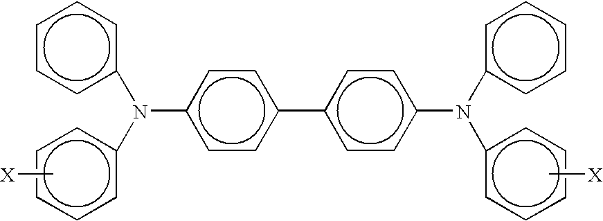
- charge transport components are aryl amines of the following formulas/structures
- X is a suitable hydrocarbon like alkyl, alkoxy, aryl, and derivatives thereof; a halogen, or mixtures thereof, and especially those substituents selected from the group consisting of Cl and CH 3 ; and molecules of the following formulas
- X, Y and Z are independently alkyl, alkoxy, aryl, a halogen, or mixtures thereof, and wherein at least one of Y and Z are present.
- Alkyl and alkoxy contain, for example, from 1 to about 25 carbon atoms, and more specifically, from 1 to about 12 carbon atoms, such as methyl, ethyl, propyl, butyl, pentyl, and the corresponding alkoxides.
- Aryl can contain from 6 to about 36 carbon atoms, such as phenyl, and the like.
- Halogen includes chloride, bromide, iodide, and fluoride. Substituted alkyls, alkoxys, and aryls can also be selected in embodiments.
- Examples of specific aryl amines that can be selected for the charge transport layer include N,N′-diphenyl-N,N′-bis(alkylphenyl)-1,1-biphenyl-4,4′-diamine wherein alkyl is selected from the group consisting of methyl, ethyl, propyl, butyl, hexyl, and the like; N,N′-diphenyl-N,N′-bis(halophenyl)-1,1-biphenyl-4,4′-diamine wherein the halo substituent is a chloro substituent; N,N′-bis(4-butylphenyl)-N,N′-di-p-tolyl-[p-terphenyl]-4,4′-diamine, N,N′-bis-(4-butylphenyl)-N,N′-di-m-tolyl-[p-terphenyl]-4,4′-diamine, N
- binder materials selected for the charge transport layers include polycarbonates, polyarylates, acrylate polymers, vinyl polymers, cellulose polymers, polyesters, polysiloxanes, polyamides, polyurethanes, poly(cyclo olefins), epoxies, and random or alternating copolymers thereof; and more specifically, polycarbonates such as poly(4,4′-isopropylidene-diphenylene)carbonate (also referred to as bisphenol-A-polycarbonate), poly(4,4′-cyclohexylidinediphenylene)carbonate (also referred to as bisphenol-Z-polycarbonate), poly(4,4′-isopropylidene-3,3′-dimethyl-diphenyl)carbonate (also referred to as bisphenol-C-polycarbonate), and the like.
- polycarbonates such as poly(4,4′-isopropylidene-diphenylene)carbonate (also referred to as bisphenol-A-pol
- electrically inactive binders are comprised of polycarbonate resins with a molecular weight of from about 20,000 to about 100,000, or with a molecular weight M w of from about 50,000 to about 100,000.
- the transport layer contains from about 10 to about 75 percent by weight of the charge transport material, and more specifically, from about 35 percent to about 50 percent of this material.
- the charge transport layer or layers, and more specifically, a first charge transport in contact with the photogenerating layer, and thereover a top or second charge transport layer may comprise charge transporting small molecules dissolved or molecularly dispersed in a film forming electrically inert polymer such as a polycarbonate.
- dissolved refers, for example, to forming a solution in which the small molecule is dissolved in the polymer to form a homogeneous phase
- “molecularly dispersed in embodiments” refers, for example, to charge transporting molecules dispersed in the polymer, the small molecules being dispersed in the polymer on a molecular scale.
- charge transport refers, for example, to charge transporting molecules as a monomer that allows the free charge generated in the photogenerating layer to be transported across the transport layer.
- Examples of hole transporting molecules present in the charge transport layer, or layers, for example, in an amount of from about 50 to about 75 weight percent include, for example, pyrazolines such as 1-phenyl-3-(4′-diethylamino styryl)-5-(4′′-diethylamino phenyl)pyrazoline; aryl amines such as N,N′-diphenyl-N,N′-bis(3-methylphenyl)-(1,1′-biphenyl)-4,4′-diamine, N,N′-bis(4-butylphenyl)-N,N′-di-p-tolyl-[p-terphenyl]-4,4′-diamine, N,N′-bis(4-butylphenyl)-N,N′-di-m-tolyl-[p-terphenyl]-4,4′-diamine, N,N′-bis(4-butylphenyl)-N,N
- the charge transport layer should be substantially free (less than about two percent) of di or triamino-triphenyl methane.
- a small molecule charge transporting compound that permits injection of holes into the photogenerating layer with high efficiency and transports them across the charge transport layer with short transit times includes N,N′-diphenyl-N,N′bis(3-methylphenyl)-(1,1′-biphenyl)-4,4′-diamine, N′-bis(4-butylphenyl)-N,N′-di-p-tolyl-[p-terphenyl]-4,4′-diamine, N,N′-bis(4-butylphenyl)-N,N′-di-m-tolyl-[p-terphenyl]-4,4′-diamine, N,N′-bis(4-butylphenyl)-N,N′-di-o-
- a number of processes may be used to mix, and thereafter apply the charge transport layer or layers coating mixture to the photogenerating layer.
- Typical application techniques include spraying, dip coating, roll coating, wire wound rod coating, and the like.
- Drying of the charge transport deposited coating may be effected by any suitable conventional technique such as oven drying, infrared radiation drying, air drying, and the like.
- each of the charge transport layers in embodiments is from about 10 to about 70 micrometers, but thicknesses outside this range may in embodiments also be selected.
- the charge transport layer should be an insulator to the extent that an electrostatic charge placed on the hole transport layer is not usually conducted in the absence of illumination at a rate sufficient to prevent formation and retention of an electrostatic latent image thereon.
- the ratio of the thickness of the charge transport layer to the photogenerating layer can be from about 2:1 to 200:1, and in some instances about 400:1.
- the charge transport layer is substantially nonabsorbing to visible light or radiation in the region of intended use, but is electrically “active” in that it allows the injection of photogenerated holes from the photoconductive layer, or photogenerating layer, and allows these holes to be transported through itself to selectively discharge a surface charge on the surface of the active layer.
- Typical application techniques include spraying, dip coating, roll coating, wire wound rod coating, and the like. Drying of the deposited coating may be effected by any suitable conventional technique, such as oven drying, infrared radiation drying, air drying, and the like.
- An optional overcoating may be applied over the charge transport layer to provide abrasion protection.
- Examples of components or materials optionally incorporated into the charge transport layers or at least one charge transport layer to, for example, enable excellent lateral charge migration (LCM) resistance include hindered phenolic antioxidants, such as tetrakis methylene(3,5-di-tert-butyl-4-hydroxy hydrocinnamate) methane (IRGANOXTM 1010, available from Ciba Specialty Chemical), butylated hydroxytoluene (BHT), and other hindered phenolic antioxidants including SUMILIZERTM BHT-R, MDP-S, BBM-S, WX-R, NW, BP-76, BP-101, GA-80, GM and GS (available from Sumitomo Chemical Co., Ltd.), IRGANOXTM 1035, 1076, 1098, 1135, 1141, 1222, 1330, 1425WL, 1520L, 245, 259, 3114, 3790, 5057 and 565 (available from Ciba Specialties Chemicals), and
- the present disclosure in embodiments thereof relates to a photoconductive member comprised of a supporting substrate, a photogenerating layer, a light shock reducing additive containing charge transport layer, and an overcoating charge transport layer; a photoconductive member with a photogenerating layer of a thickness of from about 0.1 to about 10 microns, and at least one transport layer each of a thickness of from about 5 to about 100 microns; a member wherein the thickness of the photogenerating layer is from about 0.1 to about 4 microns; a member or photoconductor wherein the photogenerating layer contains a polymer binder; a member wherein the binder is present in an amount of from about 50 to about 90 percent by weight, and wherein the total of all layer components is about 100 percent; a member wherein the photogenerating component is a hydroxygallium phthalocyanine that absorbs light of a wavelength of from about 370 to about 950 nanometers; an imaging member wherein the supporting substrate is comprised of a conductive substrate comprised of a metal; an imaging member
- X is selected from the group consisting of lower, that is with, for example, from 1 to about 8 carbon atoms, alkyl, alkoxy, aryl, and halogen; a photoconductor wherein each of, or at least one of the charge transport layers comprises
- X and Y are independently lower alkyl, lower alkoxy, phenyl, a halogen, or mixtures thereof, and wherein the photogenerating and charge transport layer resinous binder is selected from the group consisting of polycarbonates and polystyrene; a photoconductor wherein the photogenerating pigment present in the photogenerating layer is comprised of chlorogallium phthalocyanine, or Type V hydroxygallium phthalocyanine prepared by hydrolyzing a gallium phthalocyanine precursor by dissolving the hydroxygallium phthalocyanine in a strong acid, and then reprecipitating the resulting dissolved precursor in a basic aqueous media; removing any ionic species formed by washing with water; concentrating the resulting aqueous slurry comprised of water and hydroxygallium phthalocyanine to a wet cake; removing water from the wet cake by drying; and subjecting the resulting dry pigment to mixing with the addition of a second solvent to cause the formation of the hydroxy
- a dispersion of a hole blocking layer was prepared by milling 18 grams of TiO 2 (MT-150W, manufactured by Tayca Co., Japan), 24 grams of a phenolic resin (VARCUM® 29159, OxyChem Co.) at a solid weight ratio of about 60 to about 40 in a solvent of about 50 to about 50 in weight of xylene and 1-butanol, and a total solid content of about 52 percent in an Attritor mill with about 0.4 to about 0.6 millimeter size ZrO 2 beads for 6.5 hours, and then filtering with a 20 micron Nylon filter.
- TiO 2 MT-150W, manufactured by Tayca Co., Japan
- VARCUM® 29159 phenolic resin
- OxyChem Co. phenolic resin
- methyl ethyl ketone in a solvent mixture of xylene, 1-butanol at a weight ratio of 47.5:47.5:5 (xylene:butanol:ketone).
- a photogenerating layer at a thickness of about 0.2 micron comprising chlorogallium phthalocyanine (Type B) was disposed on the above hole blocking layer or undercoat layer at a thickness of about 10 microns.
- the photogenerating layer coating dispersion was prepared as follows: 2.7 grams of chlorogallium phthalocyanine (ClGaPc) Type B pigment was mixed with 2.3 grams of polymeric binder (carboxyl-modified vinyl copolymer, VMCH, Dow Chemical Company), 15 grams of n-butyl acetate and 30 grams of xylene. The mixture was milled in an attritor mill with about 200 grams of 1 millimeter Hi-Bea borosilicate glass beads for about 3 hours. The dispersion was filtered through a 20 micron Nylon cloth filter, and the solid content of the dispersion was diluted to about 6 weight percent.
- PTFE POLYFLONTM L-2 microparticle (1 gram) available from Daikin Industries dissolved/dispersed in a solvent mixture of 20 grams of tetrahydrofuran (THF), and 6.7 grams of toluene via a CAVIPROTM 300 nanomizer (Five Star Technology, Cleveland, Ohio).
- THF tetrahydrofuran
- CAVIPROTM 300 nanomizer Fe Star Technology, Cleveland, Ohio
- the resulting hole blocking layer had a dry thickness of 500 Angstroms.
- An adhesive layer was then deposited by applying a wet coating over the blocking layer, using a gravure applicator or an extrusion coater, and which adhesive contained 0.2 percent by weight based on the total weight of the solution of the copolyester adhesive (ARDEL D100TM available from Toyota Hsutsu Inc.) in a 60:30:10 volume ratio mixture of tetrahydrofuran/monochlorobenzene/methylene chloride. The adhesive layer was then dried for about 1 minute at 120° C. in the forced air dryer of the coater. The resulting adhesive layer had a dry thickness of 200 Angstroms.
- a photogenerating layer dispersion was prepared by introducing 0.45 gram of the known polycarbonate IUPILON 200TM (PCZ-200) weight average molecular weight of 20,000, available from Mitsubishi Gas Chemical Corporation, and 50 milliliters of tetrahydrofuran into a 4 ounce glass bottle. To this solution were added 2.4 grams of hydroxygallium phthalocyanine (Type V) and 300 grams of 1 ⁇ 8 inch (3.2 millimeters) diameter stainless steel shot. This mixture was then placed on a ball mill for 8 hours. Subsequently, 2.25 grams of PCZ-200 were dissolved in 46.1 grams of tetrahydrofuran, and added to the hydroxygallium phthalocyanine dispersion.
- PCZ-200 polycarbonate
- Type V hydroxygallium phthalocyanine
- This slurry was then placed on a shaker for 10 minutes.
- the resulting dispersion was, thereafter, applied to the above adhesive interface with a Bird applicator to form a photogenerating layer having a wet thickness of 0.25 mil.
- a strip about 10 millimeters wide along one edge of the substrate web bearing the blocking layer and the adhesive layer was deliberately left uncoated by any of the photogenerating layer material to facilitate adequate electrical contact by the ground strip layer of that was applied later.
- the photogenerating layer was dried at 120° C. for 1 minute in a forced air oven to form a dry photogenerating layer having a thickness of 0.4 micron.
- the resulting photoconductor web was then coated with a dual charge transport layer.
- the first charge transport layer was prepared by introducing into an amber glass bottle in a weight ratio of 50/50, N,N′-bis(methylphenyl)-1,1-biphenyl-4,4′-diamine (TBD) and poly(4,4′-isopropylidene diphenyl) carbonate, a known bisphenol A polycarbonate having a M w molecular weight average of about 120,000, commercially available from Wegriken Bayer A.G. as MAKROLON® 5705.
- the resulting mixture was then dissolved in methylene chloride to form a solution containing 15.6 percent by weight solids. This solution was applied on the photogenerating layer to form the charge transport layer coating that upon drying (120° C. for 1 minute) had a thickness of 16.5 microns. During this coating process, the humidity was equal to or less than 30 percent, for example 25 percent.
- the above first pass charge transport layer (CTL) was then overcoated with a second top charge transport layer in a second pass.
- the charge transport layer solution of the top layer was prepared introducing into an amber glass bottle in a weight ratio of 35/65, N,N′-bis(methylphenyl)-1,1-biphenyl-4,4′-diamine (TBD) and poly(4,4′-isopropylidene diphenyl)carbonate, a known bisphenol A polycarbonate having a M w molecular weight average of about 120,000, commercially available from Wegriken Bayer A.G. as MAKROLON® 5705.
- the resulting mixture was then dissolved in methylene chloride to form a solution containing 15.6 percent by weight solids.
- This solution was applied, using a 2 mil Bird bar, on the bottom layer of the charge transport layer to form a coating that upon drying (120° C. for 1 minute) had a thickness of 16.5 microns. During this coating process the humidity was equal to or less than 15 percent.
- the total two-layer CTL thickness was 33 microns.
- a photoconductor was prepared by repeating the process of Comparative Example I except that there was included in the charge transport layer 0.1 percent by weight of the additive alpha, alpha-dimethoxy-alpha-phenylacetophenone (available as IRGACURE® 651, Ciba Specialty Chemicals, Basel, Switzerland), and subsequently, the charge transport layer dispersion components were mixed for about 10 hours before coating this dispersion on the photogenerating layer.
- the additive alpha, alpha-dimethoxy-alpha-phenylacetophenone available as IRGACURE® 651, Ciba Specialty Chemicals, Basel, Switzerland
- a photoconductor is prepared by repeating the process of Comparative Example 2 except that there is included in the first charge transport layer 0.5 percent by weight of the additive alpha, alpha-dimethoxy-alpha-phenylacetophenone (IRGACURE® 651, Ciba Specialty Chemicals, Basel, Switzerland), and subsequently, the charge transport layer solution components are mixed for at about 10 hours before coating this dispersion on the photogenerating layer.
- IRGACURE® 651 alpha-dimethoxy-alpha-phenylacetophenone
- a photoconductor is prepared by repeating the process of Example I except that there is included in the charge transport layer 0.2 percent by weight of the additive 2-hydroxy-1-[4-(2-hydroxyethoxy)phenyl]-2-methyl-1-propanone (IRGACURE® 2959, Ciba Specialty Chemicals, Basel, Switzerland), and the charge transport layer dispersion is then allowed to mix for at least 8 hours, such as about 12 hours.
- IRGACURE® 2959 2-hydroxy-1-[4-(2-hydroxyethoxy)phenyl]-2-methyl-1-propanone
- a photoconductor is prepared by repeating the process of Example I except that there is included in the charge transport layer 0.4 percent by weight of the additive anisoin (Aldrich Chemicals), and the charge transport layer dispersion is then allowed to mix for at least 8 hours, such as about 12 hours.
- the additive anisoin Aldrich Chemicals
- a photoconductor is prepared by repeating the process of Example I except that there is included in the charge transport layer 0.4 percent by weight of the additive 2,2-diethoxyacetophenone (FIRSTCURE® DEAP, Albemarle Corporation, Baton Rouge, La.), and the charge transport layer dispersion is then allowed to mix for at least 8 hours, such as about 12 hours.
- FIRSTCURE® DEAP 2,2-diethoxyacetophenone
- the above prepared photoconductors of Comparative Example 1 and Example I were tested in a scanner set to obtain photoinduced discharge cycles, sequenced at one charge-erase cycle followed by one charge-expose-erase cycle, wherein the light intensity was incrementally increased with cycling to produce a series of photoinduced discharge characteristic curves from which the photosensitivity and surface potentials at various exposure intensities were measured. Additional electrical characteristics were obtained by a series of charge-erase cycles with incrementing surface potential to generate several voltages versus charge density curves.
- the scanner was equipped with a scorotron set to a constant voltage charging at various surface potentials.
- the devices were tested at surface potentials of 700 volts with the exposure light intensity incrementally increased by means of regulating a series of neutral density filters, and the exposure light source was a 780 nanometer light emitting diode.
- the xerographic simulation was completed in an environmentally controlled light tight chamber at ambient conditions (40 percent relative humidity and 22° C.).
- the photoconductors of Comparative Example 1 and Example I exhibited substantially identical PIDCs. Thus, incorporation of the additive into the charge transport layer did not significantly adversely affect the electrical properties of the Example I photoconductor.
- V (2.8 ergs/cm 2 ) which is the surface potential of the photoconductors when the exposure was 2.8 ergs/cm 2 , was used to characterize the photoconductors.
- V (2.8 ergs/cm 2 ) was reduced quickly after exposure, for example 5 minutes after, and then the photoconductor tended to recover from this surface potential drop by light exposure after a period of rest, for example 24 hours later.
- Example I The disclosed photoconductor device (Example I) exhibited a 22V decrease in V (2.8 ergs/cm 2 ) whereas the controlled photoconductor of Comparative Example 1 exhibited a 54V decrease in V (2.8 ergs/cm 2 ) after light exposure, which indicated that the Example I photoconductor was more light shock resistant with less drop in V (2.8 ergs/cm 2 ) after light exposure.
- incorporation of the above ketal additive in the charge transport layer improved light shock resistance with the initial drop in V (2.8 ergs/cm 2 ) being about one half of that of the Comparative Example 1 photoconductor with no additive in the charge transport layer.
- V (2.8 ergs/cm 2 ) should usually remain unchanged whether the photoconductor is exposed to light or not.
- the light shock resistant Example I photoconductor did not xerographically print dark bands even when the photoconductor was exposed to white light.
Abstract
Description

wherein R1, R2, R3, and R4 are each independently at least one of hydrogen, alkyl, and aryl.

wherein each R substituent is, for example, hydrogen, alkyl, aryl, substituted alkyl, substituted aryl, and the like:


wherein each R substituent is hydrogen, alkyl, aryl, substituted derivatives thereof, and the like as illustrated herein.


wherein each R substituent is hydrogen, alkyl, aryl, substituted derivatives thereof, and the like.


wherein X is a suitable hydrocarbon like alkyl, alkoxy, aryl, and derivatives thereof; a halogen, or mixtures thereof, and especially those substituents selected from the group consisting of Cl and CH3; and molecules of the following formulas

wherein X, Y and Z are independently alkyl, alkoxy, aryl, a halogen, or mixtures thereof, and wherein at least one of Y and Z are present.
wherein X is selected from the group consisting of lower, that is with, for example, from 1 to about 8 carbon atoms, alkyl, alkoxy, aryl, and halogen; a photoconductor wherein each of, or at least one of the charge transport layers comprises

wherein X and Y are independently lower alkyl, lower alkoxy, phenyl, a halogen, or mixtures thereof, and wherein the photogenerating and charge transport layer resinous binder is selected from the group consisting of polycarbonates and polystyrene; a photoconductor wherein the photogenerating pigment present in the photogenerating layer is comprised of chlorogallium phthalocyanine, or Type V hydroxygallium phthalocyanine prepared by hydrolyzing a gallium phthalocyanine precursor by dissolving the hydroxygallium phthalocyanine in a strong acid, and then reprecipitating the resulting dissolved precursor in a basic aqueous media; removing any ionic species formed by washing with water; concentrating the resulting aqueous slurry comprised of water and hydroxygallium phthalocyanine to a wet cake; removing water from the wet cake by drying; and subjecting the resulting dry pigment to mixing with the addition of a second solvent to cause the formation of the hydroxygallium phthalocyanine; an imaging member wherein the Type V hydroxygallium phthalocyanine has major peaks, as measured with an X-ray diffractometer, at Bragg angles (2 theta+/−0.2°) 7.4, 9.8, 12.4, 16.2, 17.6, 18.4, 21.9, 23.9, 25.0, 28.1 degrees, and the highest peak at 7.4 degrees; a method of imaging which comprises generating an electrostatic latent image on the photoconductor developing the latent image, and transferring the developed electrostatic image to a suitable substrate; a method of imaging wherein the imaging member is exposed to light of a wavelength of from about 370 to about 950 nanometers; a member wherein the photogenerating layer is of a thickness of from about 0.1 to about 50 microns; a member wherein the photogenerating pigment is dispersed in from about 1 weight percent to about 80 weight percent of a polymer binder; a member wherein the binder is present in an amount of from about 50 to about 90 percent by weight, and wherein the total of the layer components is about 100 percent; a photoconductor wherein the photogenerating component is Type V hydroxygallium phthalocyanine, or chlorogallium phthalocyanine, and the charge transport layer contains a hole transport of N,N′-diphenyl-N,N-bis(3-methylphenyl)-1,1′-biphenyl-4,4′-diamine, N,N′-bis(4-butylphenyl)-N,N′-di-p-tolyl-[p-terphenyl]-4,4′-diamine, N,N′-bis(4-butylphenyl)-N,N′-di-m-tolyl-[p-terphenyl]-4,4′-diamine, N,N′-bis(4-butylphenyl)-N,N′-di-o-tolyl-[p-terphenyl]-4,4′-diamine, N,N′-bis(4-butylphenyl)-N,N′-bis-(4-isopropylphenyl)-[p-terphenyl]-4,4′-diamine, N,N′-bis(4-butylphenyl)-N,N′-bis-(2-ethyl-6-methylphenyl)-[p-terphenyl]-4,4′-diamine, N,N′-bis(4-butylphenyl)-N,N′-bis-(2,5-dimethylphenyl)-[p-terphenyl]-4,4′-diamine, N,N′-diphenyl-N,N′-bis(3-chlorophenyl)-[p-terphenyl]-4,4′-diamine molecules, and wherein the hole transport resinous binder is selected from the group consisting of polycarbonates and polystyrene; an imaging member wherein the photogenerating layer contains a metal free phthalocyanine; a photoconductive imaging member comprised of a supporting substrate, a doped photogenerating layer, a hole transport layer, and in embodiments wherein a plurality of charge transport layers are selected, such as for example, from two to about ten, and more specifically two, may be selected; and a photoconductive imaging member comprised of an optional supporting substrate, a photogenerating layer, and a first, second, and third charge transport layer.
| TABLE 1 | ||
| V(2.8 ergs/cm2) (V) | Shielded Bottom Half | Exposed Top Half |
| Comparative Example 1 | 255 | 201 |
| Example I | 263 | 241 |
Claims (32)


Priority Applications (1)
| Application Number | Priority Date | Filing Date | Title |
|---|---|---|---|
| US11/961,462 US7972756B2 (en) | 2007-12-20 | 2007-12-20 | Ketal containing photoconductors |
Applications Claiming Priority (1)
| Application Number | Priority Date | Filing Date | Title |
|---|---|---|---|
| US11/961,462 US7972756B2 (en) | 2007-12-20 | 2007-12-20 | Ketal containing photoconductors |
Publications (2)
| Publication Number | Publication Date |
|---|---|
| US20090162765A1 US20090162765A1 (en) | 2009-06-25 |
| US7972756B2 true US7972756B2 (en) | 2011-07-05 |
Family
ID=40789051
Family Applications (1)
| Application Number | Title | Priority Date | Filing Date |
|---|---|---|---|
| US11/961,462 Expired - Fee Related US7972756B2 (en) | 2007-12-20 | 2007-12-20 | Ketal containing photoconductors |
Country Status (1)
| Country | Link |
|---|---|
| US (1) | US7972756B2 (en) |
Cited By (1)
| Publication number | Priority date | Publication date | Assignee | Title |
|---|---|---|---|---|
| US20110136049A1 (en) * | 2009-12-08 | 2011-06-09 | Xerox Corporation | Imaging members comprising fluoroketone |
Families Citing this family (3)
| Publication number | Priority date | Publication date | Assignee | Title |
|---|---|---|---|---|
| US20090162767A1 (en) * | 2007-12-20 | 2009-06-25 | Xerox Corporation | Benzophenone containing photoconductors |
| US7867675B2 (en) | 2007-12-20 | 2011-01-11 | Xerox Corporation | Nitrogen heterocyclics in photoconductor charge transport layer |
| JP2018060061A (en) * | 2016-10-05 | 2018-04-12 | コニカミノルタ株式会社 | Electrophotographic photoreceptor and image forming apparatus |
Citations (14)
| Publication number | Priority date | Publication date | Assignee | Title |
|---|---|---|---|---|
| US4265990A (en) | 1977-05-04 | 1981-05-05 | Xerox Corporation | Imaging system with a diamine charge transport material in a polycarbonate resin |
| US4587189A (en) | 1985-05-24 | 1986-05-06 | Xerox Corporation | Photoconductive imaging members with perylene pigment compositions |
| US4921769A (en) | 1988-10-03 | 1990-05-01 | Xerox Corporation | Photoresponsive imaging members with polyurethane blocking layers |
| US5473064A (en) | 1993-12-20 | 1995-12-05 | Xerox Corporation | Hydroxygallium phthalocyanine imaging members and processes |
| US5482811A (en) | 1994-10-31 | 1996-01-09 | Xerox Corporation | Method of making hydroxygallium phthalocyanine type V photoconductive imaging members |
| US5521306A (en) | 1994-04-26 | 1996-05-28 | Xerox Corporation | Processes for the preparation of hydroxygallium phthalocyanine |
| US6913863B2 (en) | 2003-02-19 | 2005-07-05 | Xerox Corporation | Photoconductive imaging members |
| US7037631B2 (en) | 2003-02-19 | 2006-05-02 | Xerox Corporation | Photoconductive imaging members |
| US20060105254A1 (en) | 2004-11-18 | 2006-05-18 | Xerox Corporation. | Processes for the preparation of high sensitivity titanium phthalocyanines photogenerating pigments |
| US20090162767A1 (en) | 2007-12-20 | 2009-06-25 | Xerox Corporation | Benzophenone containing photoconductors |
| US7846627B2 (en) | 2007-12-20 | 2010-12-07 | Xerox Corporation | Aminoketone containing photoconductors |
| US7855039B2 (en) * | 2007-12-20 | 2010-12-21 | Xerox Corporation | Photoconductors containing ketal overcoats |
| US7867675B2 (en) | 2007-12-20 | 2011-01-11 | Xerox Corporation | Nitrogen heterocyclics in photoconductor charge transport layer |
| US7897310B2 (en) | 2007-12-20 | 2011-03-01 | Xerox Corporation | Phosphine oxide containing photoconductors |
-
2007
- 2007-12-20 US US11/961,462 patent/US7972756B2/en not_active Expired - Fee Related
Patent Citations (14)
| Publication number | Priority date | Publication date | Assignee | Title |
|---|---|---|---|---|
| US4265990A (en) | 1977-05-04 | 1981-05-05 | Xerox Corporation | Imaging system with a diamine charge transport material in a polycarbonate resin |
| US4587189A (en) | 1985-05-24 | 1986-05-06 | Xerox Corporation | Photoconductive imaging members with perylene pigment compositions |
| US4921769A (en) | 1988-10-03 | 1990-05-01 | Xerox Corporation | Photoresponsive imaging members with polyurethane blocking layers |
| US5473064A (en) | 1993-12-20 | 1995-12-05 | Xerox Corporation | Hydroxygallium phthalocyanine imaging members and processes |
| US5521306A (en) | 1994-04-26 | 1996-05-28 | Xerox Corporation | Processes for the preparation of hydroxygallium phthalocyanine |
| US5482811A (en) | 1994-10-31 | 1996-01-09 | Xerox Corporation | Method of making hydroxygallium phthalocyanine type V photoconductive imaging members |
| US6913863B2 (en) | 2003-02-19 | 2005-07-05 | Xerox Corporation | Photoconductive imaging members |
| US7037631B2 (en) | 2003-02-19 | 2006-05-02 | Xerox Corporation | Photoconductive imaging members |
| US20060105254A1 (en) | 2004-11-18 | 2006-05-18 | Xerox Corporation. | Processes for the preparation of high sensitivity titanium phthalocyanines photogenerating pigments |
| US20090162767A1 (en) | 2007-12-20 | 2009-06-25 | Xerox Corporation | Benzophenone containing photoconductors |
| US7846627B2 (en) | 2007-12-20 | 2010-12-07 | Xerox Corporation | Aminoketone containing photoconductors |
| US7855039B2 (en) * | 2007-12-20 | 2010-12-21 | Xerox Corporation | Photoconductors containing ketal overcoats |
| US7867675B2 (en) | 2007-12-20 | 2011-01-11 | Xerox Corporation | Nitrogen heterocyclics in photoconductor charge transport layer |
| US7897310B2 (en) | 2007-12-20 | 2011-03-01 | Xerox Corporation | Phosphine oxide containing photoconductors |
Non-Patent Citations (14)
| Title |
|---|
| Jin Wu et al., U.S. Appl. No. 11/472,765 on Titanyl Phthalocyanine Photoconductors, filed Jun. 22, 2006. |
| Jin Wu et al., U.S. Appl. No. 11/472,766 on Titanyl Phthalocyanine Photoconductors, filed Jun. 22, 2006. |
| Jin Wu et al., U.S. Appl. No. 11/848,428 on Photoconductors, filed Aug. 31, 2007. |
| Jin Wu et al., U.S. Appl. No. 11/869,231 on Additive Containing Photogenerating Layer Photoconductors, filed Oct. 9, 2007. |
| Jin Wu et al., U.S. Appl. No. 11/869,252 on Additive Containing Charge Transport Layer Photoconductors, filed Oct. 9, 2007. |
| Jin Wu et al., U.S. Appl. No. 11/869,258 on Imidazolium Salt Containing Charge Transport Layer Photoconductors, filed Oct. 9, 2007. |
| Jin Wu et al., U.S. Appl. No. 11/869,269 on Charge Trapping Releaser Containing Charge Transport Layer Photoconductors, filed Oct. 9, 2007. |
| Jin Wu, U.S. Appl. No. 11/831,440 on Additive Containing Photogenerating Layer Photoconductors, filed Jul. 31, 2007. |
| Jin Wu, U.S. Appl. No. 11/848,417 on Light Stabilizer Containing Photoconductors, filed Aug. 31, 2007. |
| Jin Wu, U.S. Appl. No. 11/848,439 on Boron Containing Photoconductors, filed Aug. 31, 2007. |
| Jin Wu, U.S. Appl. No. 11/848,448 on Triazole Containing Photoconductors, filed Aug. 31, 2007. |
| Liang-Bih Lin et al., U.S. Appl. No. 11/800,108 on Photoconductors, filed May 4, 2007. |
| Liang-Bih Lin et al., U.S. Appl. No. 11/800,129 on Photoconductors, filed May 4, 2007. |
| Liang-Bih Lin et al., U.S. Appl. No. 11/848,454 on Hydroxy Benzophenone Containing Photoconductors, filed Aug. 31, 2007. |
Cited By (1)
| Publication number | Priority date | Publication date | Assignee | Title |
|---|---|---|---|---|
| US20110136049A1 (en) * | 2009-12-08 | 2011-06-09 | Xerox Corporation | Imaging members comprising fluoroketone |
Also Published As
| Publication number | Publication date |
|---|---|
| US20090162765A1 (en) | 2009-06-25 |
Similar Documents
| Publication | Publication Date | Title |
|---|---|---|
| US7989127B2 (en) | Carbazole containing charge transport layer photoconductors | |
| US20090162767A1 (en) | Benzophenone containing photoconductors | |
| US7811732B2 (en) | Titanocene containing photoconductors | |
| US7776499B2 (en) | Overcoat containing fluorinated poly(oxetane) photoconductors | |
| EP2290452B1 (en) | POSS melamine overcoated photoconductors | |
| US8012657B2 (en) | Phenol polysulfide containing photogenerating layer photoconductors | |
| US8003289B2 (en) | Ferrocene containing photoconductors | |
| US7560206B2 (en) | Photoconductors with silanol-containing photogenerating layer | |
| US20100330476A1 (en) | Polyfluorinated core shell photoconductors | |
| US7709169B2 (en) | Charge trapping releaser containing charge transport layer photoconductors | |
| US8119316B2 (en) | Thiuram tetrasulfide containing photogenerating layer | |
| US7960080B2 (en) | Oxadiazole containing photoconductors | |
| US7867675B2 (en) | Nitrogen heterocyclics in photoconductor charge transport layer | |
| US7935466B2 (en) | Benzothiazole containing photogenerating layer | |
| US20090061340A1 (en) | Hydroxy benzophenone containing photoconductors | |
| US7972756B2 (en) | Ketal containing photoconductors | |
| US7687212B2 (en) | Charge trapping releaser containing photogenerating layer photoconductors | |
| US7897310B2 (en) | Phosphine oxide containing photoconductors | |
| US7846627B2 (en) | Aminoketone containing photoconductors | |
| US7989126B2 (en) | Metal mercaptoimidazoles containing photoconductors | |
| US7662526B2 (en) | Photoconductors | |
| US7923185B2 (en) | Pyrazine containing charge transport layer photoconductors | |
| US7855039B2 (en) | Photoconductors containing ketal overcoats | |
| US7951515B2 (en) | Ester thiols containing photogenerating layer photoconductors | |
| US7914961B2 (en) | Salt additive containing photoconductors |
Legal Events
| Date | Code | Title | Description |
|---|---|---|---|
| AS | Assignment |
Owner name: XEROX CORPORATION,CONNECTICUT Free format text: ASSIGNMENT OF ASSIGNORS INTEREST;ASSIGNOR:WU, JIN , ,;REEL/FRAME:020346/0364 Effective date: 20071210 Owner name: XEROX CORPORATION, CONNECTICUT Free format text: ASSIGNMENT OF ASSIGNORS INTEREST;ASSIGNOR:WU, JIN , ,;REEL/FRAME:020346/0364 Effective date: 20071210 |
|
| FEPP | Fee payment procedure |
Free format text: PAYOR NUMBER ASSIGNED (ORIGINAL EVENT CODE: ASPN); ENTITY STATUS OF PATENT OWNER: LARGE ENTITY |
|
| STCF | Information on status: patent grant |
Free format text: PATENTED CASE |
|
| FPAY | Fee payment |
Year of fee payment: 4 |
|
| FEPP | Fee payment procedure |
Free format text: MAINTENANCE FEE REMINDER MAILED (ORIGINAL EVENT CODE: REM.); ENTITY STATUS OF PATENT OWNER: LARGE ENTITY |
|
| LAPS | Lapse for failure to pay maintenance fees |
Free format text: PATENT EXPIRED FOR FAILURE TO PAY MAINTENANCE FEES (ORIGINAL EVENT CODE: EXP.); ENTITY STATUS OF PATENT OWNER: LARGE ENTITY |
|
| STCH | Information on status: patent discontinuation |
Free format text: PATENT EXPIRED DUE TO NONPAYMENT OF MAINTENANCE FEES UNDER 37 CFR 1.362 |
|
| FP | Lapsed due to failure to pay maintenance fee |
Effective date: 20190705 |