US7993957B2 - Phase change memory cell and manufacturing method thereof using minitrenches - Google Patents
Phase change memory cell and manufacturing method thereof using minitrenches Download PDFInfo
- Publication number
- US7993957B2 US7993957B2 US11/045,170 US4517005A US7993957B2 US 7993957 B2 US7993957 B2 US 7993957B2 US 4517005 A US4517005 A US 4517005A US 7993957 B2 US7993957 B2 US 7993957B2
- Authority
- US
- United States
- Prior art keywords
- forming
- layer
- thin portion
- spacer
- opening
- Prior art date
- Legal status (The legal status is an assumption and is not a legal conclusion. Google has not performed a legal analysis and makes no representation as to the accuracy of the status listed.)
- Active, expires
Links
Images


Classifications
-
- H—ELECTRICITY
- H10—SEMICONDUCTOR DEVICES; ELECTRIC SOLID-STATE DEVICES NOT OTHERWISE PROVIDED FOR
- H10N—ELECTRIC SOLID-STATE DEVICES NOT OTHERWISE PROVIDED FOR
- H10N70/00—Solid-state devices without a potential-jump barrier or surface barrier, and specially adapted for rectifying, amplifying, oscillating or switching
- H10N70/20—Multistable switching devices, e.g. memristors
- H10N70/231—Multistable switching devices, e.g. memristors based on solid-state phase change, e.g. between amorphous and crystalline phases, Ovshinsky effect
-
- G—PHYSICS
- G11—INFORMATION STORAGE
- G11C—STATIC STORES
- G11C11/00—Digital stores characterised by the use of particular electric or magnetic storage elements; Storage elements therefor
- G11C11/56—Digital stores characterised by the use of particular electric or magnetic storage elements; Storage elements therefor using storage elements with more than two stable states represented by steps, e.g. of voltage, current, phase, frequency
- G11C11/5678—Digital stores characterised by the use of particular electric or magnetic storage elements; Storage elements therefor using storage elements with more than two stable states represented by steps, e.g. of voltage, current, phase, frequency using amorphous/crystalline phase transition storage elements
-
- G—PHYSICS
- G11—INFORMATION STORAGE
- G11C—STATIC STORES
- G11C13/00—Digital stores characterised by the use of storage elements not covered by groups G11C11/00, G11C23/00, or G11C25/00
- G11C13/0002—Digital stores characterised by the use of storage elements not covered by groups G11C11/00, G11C23/00, or G11C25/00 using resistive RAM [RRAM] elements
- G11C13/0004—Digital stores characterised by the use of storage elements not covered by groups G11C11/00, G11C23/00, or G11C25/00 using resistive RAM [RRAM] elements comprising amorphous/crystalline phase transition cells
-
- H—ELECTRICITY
- H10—SEMICONDUCTOR DEVICES; ELECTRIC SOLID-STATE DEVICES NOT OTHERWISE PROVIDED FOR
- H10B—ELECTRONIC MEMORY DEVICES
- H10B63/00—Resistance change memory devices, e.g. resistive RAM [ReRAM] devices
- H10B63/30—Resistance change memory devices, e.g. resistive RAM [ReRAM] devices comprising selection components having three or more electrodes, e.g. transistors
- H10B63/32—Resistance change memory devices, e.g. resistive RAM [ReRAM] devices comprising selection components having three or more electrodes, e.g. transistors of the bipolar type
-
- H—ELECTRICITY
- H10—SEMICONDUCTOR DEVICES; ELECTRIC SOLID-STATE DEVICES NOT OTHERWISE PROVIDED FOR
- H10N—ELECTRIC SOLID-STATE DEVICES NOT OTHERWISE PROVIDED FOR
- H10N70/00—Solid-state devices without a potential-jump barrier or surface barrier, and specially adapted for rectifying, amplifying, oscillating or switching
- H10N70/011—Manufacture or treatment of multistable switching devices
- H10N70/061—Patterning of the switching material
- H10N70/068—Patterning of the switching material by processes specially adapted for achieving sub-lithographic dimensions, e.g. using spacers
-
- H—ELECTRICITY
- H10—SEMICONDUCTOR DEVICES; ELECTRIC SOLID-STATE DEVICES NOT OTHERWISE PROVIDED FOR
- H10N—ELECTRIC SOLID-STATE DEVICES NOT OTHERWISE PROVIDED FOR
- H10N70/00—Solid-state devices without a potential-jump barrier or surface barrier, and specially adapted for rectifying, amplifying, oscillating or switching
- H10N70/801—Constructional details of multistable switching devices
- H10N70/821—Device geometry
- H10N70/826—Device geometry adapted for essentially vertical current flow, e.g. sandwich or pillar type devices
-
- H—ELECTRICITY
- H10—SEMICONDUCTOR DEVICES; ELECTRIC SOLID-STATE DEVICES NOT OTHERWISE PROVIDED FOR
- H10N—ELECTRIC SOLID-STATE DEVICES NOT OTHERWISE PROVIDED FOR
- H10N70/00—Solid-state devices without a potential-jump barrier or surface barrier, and specially adapted for rectifying, amplifying, oscillating or switching
- H10N70/801—Constructional details of multistable switching devices
- H10N70/841—Electrodes
- H10N70/8413—Electrodes adapted for resistive heating
-
- H—ELECTRICITY
- H10—SEMICONDUCTOR DEVICES; ELECTRIC SOLID-STATE DEVICES NOT OTHERWISE PROVIDED FOR
- H10N—ELECTRIC SOLID-STATE DEVICES NOT OTHERWISE PROVIDED FOR
- H10N70/00—Solid-state devices without a potential-jump barrier or surface barrier, and specially adapted for rectifying, amplifying, oscillating or switching
- H10N70/801—Constructional details of multistable switching devices
- H10N70/881—Switching materials
- H10N70/882—Compounds of sulfur, selenium or tellurium, e.g. chalcogenides
- H10N70/8828—Tellurides, e.g. GeSbTe
Definitions
- the present invention relates to a phase change memory cell and to a manufacturing process thereof.
- phase change memory (PCM) elements exploit the characteristics of materials which have the property of changing between two phases having distinct electrical characteristics. For example, these materials may change from an amorphous phase, which is disorderly, to a crystalline or polycrystalline phase, which is orderly, and the two phases are associated to considerably different resistivity.
- alloys of group VI of the periodic table such as Te or Se, referred to as chalcogenides or chalcogenic materials
- chalcogenides or chalcogenic materials can advantageously be used in phase change cells.
- the chalcogenide that currently offers the most promise is formed by a Ge, Sb and Te alloy (Ge 2 Sb 2 Te 5 ), which is currently widely used for storing information in overwritable disks.
- the resistivity varies by two or more magnitude orders when the material passes from the amorphous phase (more resistive) to the polycrystalline phase (more conductive) and vice versa.
- the characteristics of chalcogenides in the two phases are shown in FIG. 1 .
- Vr read voltage
- Phase change may be obtained by locally increasing the temperature, as shown in FIG. 2 . Below 150° C. both phases are stable. Above 200° C. (temperature of start of nucleation, designated by T x ), fast nucleation of the crystallites takes place, and, if the material is kept at the crystallization temperature for a sufficient length of time (time t 2 ), it changes its phase and becomes crystalline. To bring the chalcogenide back into the amorphous state, it is necessary to raise the temperature above the melting temperature T m (approximately 600° C.) and then to cool the chalcogenide off rapidly (time t 1 ).
- T m melting temperature melting temperature
- FIG. 3 The basic structure of a PCM element 1 which operates according to the principles described above is shown in FIG. 3 and comprises a resistive element 2 (heater) and a programmable element 3 .
- the programmable element 3 is made of a chalcogenide and is normally in the polycrystalline state in order to enable a good flow of current.
- One part of the programmable element 3 is in direct contact with the resistive element 2 and forms the area affected by phase change, hereinafter referred to as the phase change portion 4 .
- phase change portion 4 selectively up to the crystallization temperature or to the melting temperature and to cause phase change.
- a current I flows through a resistive element 2 having resistance R, the heat generated is equal to I 2 R.
- the PCM element of FIG. 3 for forming memory cells has already been proposed.
- the PCM element is generally associated to a selection element, such a MOS transistor, a bipolar transistor, or a diode.
- An embodiment of the present invention provides a phase change memory cell that includes a resistive element, including a first thin portion having a first sublithographic dimension in a first direction, and a memory region of a phase change material and including a second thin portion having a second sublithographic dimension in a second direction transverse to the first direction.
- the resistive element and the memory region are in direct electrical contact at the first and second thin portions and define a contact area of sublithographic extension.
- the second thin portion is delimited laterally in the second direction by spacer portions of a first dielectric material, thereby defining inclined surfaces in a third direction, transverse to said first and second directions.
- Another embodiment of the invention provides a process for manufacturing a phase change memory cell.
- the process includes forming a resistive element including a first thin portion having a first sublithographic dimension in a first direction; and forming a memory region of a phase change material and including a second thin portion having a second sublithographic dimension in a second direction transverse to the first direction.
- the first and second thin portions define a contact area of sublithographic extension.
- Forming a memory region includes forming a mold layer on top of the resistive element, forming a first lithographic opening in the mold layer, forming spacer portions in the first lithographic opening, the spacer portions defining a slit having the second sublithographic dimension; and depositing a phase change layer inside the slit.
- FIG. 1 shows the current versus voltage characteristic of a phase change material
- FIG. 2 shows the temperature versus current plot of a phase change material
- FIG. 3 shows the basic structure of a PCM memory element
- FIG. 4 shows a cross section of a wafer of semiconductor material in a manufacturing step of the cell of FIG. 3 , according to the parent patent application;
- FIG. 5 shows the layout of some masks used for forming the structure of FIG. 4 ;
- FIG. 6 is a cross-section taken along line VI-VI of FIG. 5 ;
- FIGS. 7-14 are cross-section of the structure of the above mentioned patent application, in successive manufacture steps
- FIG. 15 is a top plan view, with parts removed and at an enlarged scale, of a detail of FIG. 4 ;
- FIGS. 16 a and 16 b are top plan views, with parts removed, of a detail of FIG. 14 , in two different manufacture conditions;
- FIG. 17 shows the layout of some masks used for forming the structure of FIG. 7 , according to an embodiment of the invention.
- FIG. 18 is a cross-section similar to FIG. 8 , in a manufacture step according to an embodiment of the invention.
- FIG. 19 shows the layout of some masks used for forming the structure of FIG. 18 ;
- FIGS. 20 and 21 are cross-sections, similar to FIG. 18 , in successive manufacture steps according to an embodiment of the invention.
- FIG. 22 is a top plan view of the structure of FIG. 21 ;
- FIG. 23 is a cross-section, similar to FIG. 21 , in a subsequent manufacture step
- FIG. 24 shows the layout of same masks used for forming the structure of FIG. 23 ;
- FIG. 25 is a cross-section, similar to FIG. 14 , in a final manufacture step according to an embodiment of the invention.
- FIGS. 26 a and 26 b are top plan views of the contact area, in two different manufacture conditions.
- FIGS. 27 and 28 show two steps regarding a different embodiment.
- the parent application teaches forming the contact area as an intersection of two thin portions extending transversely with respect to one another and each of a sublithographic size.
- deposition of layers is adopted instead of a lithographic process, given that deposition makes it possible to obtain very thin layers, i.e., having a thickness much smaller than the current minimum size that can be achieved using lithographic techniques.
- a wafer 10 comprising a P-type substrate 11 is subjected to standard front end steps.
- insulation regions 12 are formed and delimit active areas 16 ; then, in succession, N-type base regions 13 , N + -type base contact regions 14 , and P + -type emitter regions 15 are implanted.
- the base regions 13 , base contact regions 14 , and emitter regions 15 form diodes that form selection elements for the memory cells.
- a first dielectric layer 18 is deposited and planarized; openings are formed in the first dielectric layer 18 above the base contact regions 13 and emitter regions 15 , and the openings are filled with tungsten to form base contacts 19 b and emitter contacts 19 a .
- the base contacts 19 b are thus in direct electrical contact with the base contact regions 13
- the emitter contacts 19 a are in direct electrical contact with the emitter regions 15 .
- the openings in the first dielectric layer 18 can be covered by a barrier layer, for example a Ti/TiN layer, before being filled with tungsten. In this way, the structure of FIG. 4 is obtained.
- FIG. 5 shows the layout of some masks used for forming the structure of FIG. 4 regarding a pair of memory cells 5 that are adjacent in a perpendicular direction to the sectional plane of FIG. 4 (Y direction).
- the figure shows a mask A used for defining the active areas 16 , a mask B used for implanting the emitter regions 15 , and a mask C for forming the openings where the base contacts 19 b and the emitter contacts 19 a are to be formed.
- FIG. 4 is a cross-section taken along line IV-IV of FIG. 5
- FIG. 6 shows the same structure sectioned along the section line VI-VI of FIG. 5 .
- a second dielectric layer 20 for example, an undoped silicon glass (USG) layer—is deposited, and openings 21 are formed in the second dielectric layer 20 above the emitter contact 19 a .
- the openings 21 have dimensions dictated by the lithographic process and are, for example, circle-shaped.
- a heating layer for example of TiSiN, TiAlN or TiSiC, is deposited for a thickness of 10-50 nm, preferably 20 nm.
- the heating layer designed to form the resistive element 2 of FIG. 3 , conformally coats the walls and bottom of the openings 21 and is subsequently removed outside the openings 21 .
- the remaining portions of the heating layer thus form a cup-shaped region 22 and are then filled with dielectric material 23 .
- a mold layer 27 for instance USG having a thickness of 20 nm, an adhesion layer 28 , for instance Ti or Si with a thickness of 5 nm, and a first delimiting layer 29 , for example nitride or another material that enables selective etching with respect to the adhesion layer 28 , are deposited in sequence.
- the first delimiting layer 29 has a thickness of, for instance, 150 nm.
- one part of the first delimiting layer 29 is removed by dry etching to form a step which has a vertical side 30 that extends vertically on top of the dielectric material 23 .
- the structure shown in FIG. 8 is thus obtained.
- a sacrificial layer 31 for example TiN with a thickness of 30 nm, is deposited conformally.
- the sacrificial layer forms a vertical wall 31 a that extends along the vertical side 30 of the first delimiting layer 29 .
- the sacrificial layer 31 is undergoes an etch back that results in removal of the horizontal portions of the sacrificial layer 31 and of part of the vertical wall 31 a .
- the thickness of the first delimiting layer 29 and the thickness of the sacrificial layer 31 as well as the time and type of etching, it is possible to obtain the desired sublithographic width W 1 for the bottom part of the remaining vertical wall 31 a.
- a second delimiting layer 35 of the same material as the first delimiting layer 29 , for example nitride, with a thickness of 300 nm, is deposited.
- the delimiting layers 29 , 35 and the vertical wall 31 a are thinned by chemical mechanical polishing (CMP).
- CMP chemical mechanical polishing
- the sacrificial region 36 is removed.
- the adhesion layer 28 is isotropically etched, and the mold layer 27 is dry etched to form a slit 37 in the mold layer 27 , the slit 37 having a width W 1 equal to the width of the sacrificial region 36 .
- a chalcogenic layer 38 for example of Ge 2 Sb 2 Te 5 with a thickness of 60 nm, is deposited conformally.
- the portion 38 a of the chalcogenic layer 38 fills the slit 37 and forms, at the intersection with the cup-shaped region 22 , a phase change region similar to the phase change portion 4 of FIG. 3 .
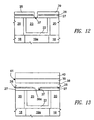
- a barrier layer 39 for example of Ti/TiN, and a metal layer 40 , for example of AlCu, are deposited.
- the structure of FIG. 13 is thus obtained.
- the stack formed by the metal layer 40 , barrier layer 39 , chalcogenic layer 38 , and adhesion layer 28 is defined using a same mask to form a bit line 41 .
- a third dielectric layer 42 is deposited, which is opened above the base contacts 19 b .
- the openings thus formed are filled with tungsten to form top contacts 43 in order to prolong upwards the base contacts 19 b .
- standard steps are performed for forming the connection lines for connection to the base contacts 19 b and to the bits lines 41 , and the final structure of FIG. 14 is thus obtained.
- the intersection between the cup-shaped region 22 and the thin portion 38 a of the chalcogenic layer 38 forms a contact area 45 which is approximately square and has sublithographic dimensions. This is due to the fact that both the cup-shaped region 22 and the thin portion 38 a have a width equal to the thickness of a deposited layer. In fact, the width of the cup-shaped region 22 is given by the thickness of the heating layer, and the width of the thin portions 38 a is determined by the thickness of the sacrificial layer 31 along the vertical side 30 .
- the cup-shaped region 22 has a sublithographic dimension in a first direction (Y direction), and the thin portion 38 a has a sublithographic dimension (width W 1 of FIG. 10 ) in a second direction (X direction) which is transverse to the first direction.
- sublithographic dimension means a linear dimension smaller than the limit dimension achievable with current optical (UV) lithographic techniques, and hence smaller than 100 nm, preferably 50-60 nm, down to approximately 20 nm.
- forming the thin portion 38 a of the chalcogenic layer 38 entails numerous steps and is somewhat complex. Consequently, it is desirable to avail a simpler alternative process.
- the dimensions of the contact area 45 depend upon the alignment tolerances between the mask used for forming the openings 21 and the mask used for removing part of the first delimiting layer 29 and for forming the vertical side 30 ( FIG. 8 ).
- FIGS. 16 a and 16 b which are top plan views of the contact area 45
- an alignment error of even only 0.05 ⁇ m between the two masks results in the thin portions 38 a no longer crossing the cup-shaped regions 22 perpendicularly, with a consequent considerable increase in the dimensions of the contact area 45 (see FIG. 16 b ) and hence a considerable increase in the flowing current, the value whereof would be uncontrollable.
- the thin portion 38 a crosses each cup-shaped region 22 in two points, thus doubling the total contact area between the thin portions 38 a and the cup-shaped regions 22 , and consequently also increasing the programming current.
- just one contact area is even obtained which has dimensions far greater than the requirements.
- the presence of a double contact gives rise to functional problems, given that in this situation it would be impossible to know which of the two contact areas 45 first causes switching of the overlying thin portion 38 a (i.e., the phase change portion), nor would it be possible to be certain that both of the thin portions 38 a overlying the two contact areas will switch.
- the process according to an embodiment of the present invention comprises initial steps equal to those described above, up to deposition of the second dielectric layer 20 ( FIG. 7 ).
- the openings 21 and the cup-shaped regions 22 are formed.
- a heater mask D is used which has rectangular windows (the term “rectangular” also comprising the particular case of a square shape). Consequently, the openings 21 have a substantially rectangular shape.
- the heating layer for example of TiSiN, TiAlN or TiSiC, with a thickness of 10-50 nm, preferably 20 nm, is deposited. The heating layer coats the walls and bottom of the openings 21 conformally.
- the cup-like regions 22 here define an ideally rectangular shape, possibly with rounded edges (on account of the lithographic limits), or at the most an ovalized shape, with the longer side, or main direction, parallel to the X direction ( FIG. 22 ).
- the heating layer is removed outside the openings 21 to form the cup-shaped regions 22 , which are then filled with the dielectric material 23 .
- a stop layer 48 for example of nitride deposited by PECVD (Plasma Enhanced Chemical Vapor Deposition) with a thickness of 40 nm
- a mold layer 49 for example of USG deposited by PECVD or SACVD (Sub-Atmospheric Chemical Vapor Deposition) with a thickness of 50-70 nm
- an adhesion layer 50 for example of Ti or Si with a thickness of 20-40 nm, are deposited in sequence.
- the adhesion layer 50 , the mold layer 49 and the stop layer 48 are etched.
- the minitrench mask E has a rectangular window that extends between two adjacent cells 5 in the Y direction (perpendicular to the alignment direction of the base and emitter regions 14 , 15 of each memory cell 5 , FIG. 7 ).
- part of the layers 48 , 49 and 50 is removed, so as to form an opening 51 having a rectangular shape, corresponding to that of the minitrench mask E.
- the width of the opening 51 in the X direction is, for example, 160 nm.
- the opening 51 uncovers part of the dielectric material 23 of the two adjacent cells 5 and crosses each cup-shaped region 22 only once, as can be clearly seen from the superposition of the heater mask D and minitrench mask E in FIG. 19 .
- a spacer layer 55 for example an oxide layer, is deposited (in particular, TEOS with a thickness of 50 nm) is deposited.
- the spacer layer 55 covers the adhesion layer 50 , as well as the walls and bottom of the opening 51 .
- the spacer layer 55 is anisotropicaily etched by etching back until the horizontal portions thereof are removed, according to the well known spacer formation technique.
- the spacer layer 55 is then completely removed above the adhesion layer 50 and is partially removed from the bottom of the opening 51 to form a spacer region 55 a which extends along the vertical sides of the opening 51 (along the perimeter of a rectangle or of an oval) and delimits a slit 56 , the base whereof forms a rectangular strip 57 having a sublithographic width W 2 (in the X direction) of approximately 60 nm.
- FIG. 21 the spacer layer 55 is anisotropicaily etched by etching back until the horizontal portions thereof are removed, according to the well known spacer formation technique.
- the spacer layer 55 is then completely removed above the adhesion layer 50 and is partially removed from the bottom of the opening 51 to form a spacer region 55 a which extends along the vertical sides of the opening 51 (along the perimeter of a rectangle or of an oval) and
- each cup-shaped region 22 is a top plan view of the structure thus obtained, and highlights how the strip 57 uncovers only one portion of the cup-shaped region 22 of each cell 5 , shown with dashed line in the figure.
- the uncovered portion of each cup-shaped region 22 forms a contact area 58 , as will be explained hereinafter.
- the chalcogenic layer 38 (also in the present case, for instance, of Ge 2 Sb 2 Te 5 with a thickness of 60 nm), the barrier layer 39 , and the metal layer 40 are deposited in succession, to form a stack of layers 41 .
- the chalcogenic layer 38 is in direct contact with the adhesion layer 50 , to which it adheres properly, and fills the slit 56 with a thin portion 38 a .
- the thin portion 38 a of the chalcogenic layer 38 deposits on the strip 57 , contacting the cup-shaped regions 22 at the contact areas 58 .
- the inclined wall formed by the spacer region 55 a favors filling of the slit 56 , so preventing problems linked to a poor aspect ratio of the opening 51 .
- the stack of layers 41 is defined using a stack mask F ( FIG. 24 ).
- the process continues with the steps described previously, which comprise deposition of the third dielectric layer 42 , opening of the third dielectric layer 42 above the base contacts 19 b , formation of the top contacts 43 , and formation of connection lines for connection to the base contacts 19 b and to the bit lines 41 , so as to obtain the final structure shown in FIG. 25 .
- the shape of the minitrench mask E makes it possible to obtain a single contact area 58 for each cup-shaped region 22 , and hence for each cell 5 , without requiring any additional masking steps.
- the rectangular or ovalized shape of the cup-shaped region 22 reduces the spread in the dimensions of the contact area 58 also when its shape, instead of being rectangular as in the ideal case, is oval, as may be seen from a comparison between FIG. 26 a , which shows the position of the cup-shaped region 22 with respect to thin region 38 a in the absence of mask misalignment, and FIG. 26 b , which shows the relative position in presence of misalignment.
- the sequence of steps required for forming the spacer region 55 a and of the strip 57 may vary.
- the spacer region 55 a is formed in the way described previously, by depositing a spacer layer and etching it anisotropically.
- the stop layer 48 is removed only where it is not covered by the spacer region 55 a , and in this way the strip 57 is uncovered.
- a protective layer 54 may be deposited, as shown in FIG. 27 .
- the protective layer 54 preferably deposited by PECVD, has, for instance, a thickness of between 20 and 30 nm.
- etching back is performed to remove the horizontal portions of the spacer layer 55 and then the horizontal portions of the protective layer 54 .
- a protective portion 54 a thus is left only beneath the spacer region 55 a , as shown in FIG. 28 .
- the protective layer 54 protects the adhesion layer 50 and prevents contamination thereof by the spacer layer 55 , which is of oxide, both at the top and at the sides. In addition, it functions as an etch stop and prevents undesired etching of the dielectric layer 20 and of the dielectric material 23 during etching back for forming the spacer region 55 a.
- a further nitride layer having a thickness of 20-30 nm is deposited. Then, using the minitrench mask E, the further nitride layer, the adhesion layer 50 , and the mold layer 49 are selectively removed, without the stop layer 48 being removed. The spacer layer 55 is deposited, and an etch back is performed for forming the spacer region 55 a . Next, a nitride etch is carried out, removing the horizontal portions of the further nitride layer above the adhesion layer 55 , and the exposed portion of the stop layer 48 . Then the other steps of depositing the chalcogenic layer 38 , and so forth, follow. In this way, the further nitride layer protects the adhesion layer 50 from any possible contamination by the spacer layer 55 .
Abstract
Description
Claims (14)
Priority Applications (2)
| Application Number | Priority Date | Filing Date | Title |
|---|---|---|---|
| US11/045,170 US7993957B2 (en) | 2002-02-20 | 2005-01-27 | Phase change memory cell and manufacturing method thereof using minitrenches |
| US13/158,291 US9876166B2 (en) | 2002-02-20 | 2011-06-10 | Phase change memory cell and manufacturing method thereof using minitrenches |
Applications Claiming Priority (6)
| Application Number | Priority Date | Filing Date | Title |
|---|---|---|---|
| EP02425087.0 | 2002-02-20 | ||
| EP02425087A EP1339110B1 (en) | 2002-02-20 | 2002-02-20 | Phase change memory cell and manufacturing method thereof using minitrenches |
| EP02425087 | 2002-02-20 | ||
| US10/313,991 US7227171B2 (en) | 2001-12-05 | 2002-12-05 | Small area contact region, high efficiency phase change memory cell and fabrication method thereof |
| US10/372,761 US6891747B2 (en) | 2002-02-20 | 2003-02-20 | Phase change memory cell and manufacturing method thereof using minitrenches |
| US11/045,170 US7993957B2 (en) | 2002-02-20 | 2005-01-27 | Phase change memory cell and manufacturing method thereof using minitrenches |
Related Parent Applications (1)
| Application Number | Title | Priority Date | Filing Date |
|---|---|---|---|
| US10/372,761 Division US6891747B2 (en) | 2002-02-20 | 2003-02-20 | Phase change memory cell and manufacturing method thereof using minitrenches |
Related Child Applications (1)
| Application Number | Title | Priority Date | Filing Date |
|---|---|---|---|
| US13/158,291 Continuation US9876166B2 (en) | 2002-02-20 | 2011-06-10 | Phase change memory cell and manufacturing method thereof using minitrenches |
Publications (2)
| Publication Number | Publication Date |
|---|---|
| US20050152208A1 US20050152208A1 (en) | 2005-07-14 |
| US7993957B2 true US7993957B2 (en) | 2011-08-09 |
Family
ID=46282014
Family Applications (3)
| Application Number | Title | Priority Date | Filing Date |
|---|---|---|---|
| US10/372,761 Expired - Lifetime US6891747B2 (en) | 2002-02-20 | 2003-02-20 | Phase change memory cell and manufacturing method thereof using minitrenches |
| US11/045,170 Active 2025-06-26 US7993957B2 (en) | 2002-02-20 | 2005-01-27 | Phase change memory cell and manufacturing method thereof using minitrenches |
| US13/158,291 Expired - Lifetime US9876166B2 (en) | 2002-02-20 | 2011-06-10 | Phase change memory cell and manufacturing method thereof using minitrenches |
Family Applications Before (1)
| Application Number | Title | Priority Date | Filing Date |
|---|---|---|---|
| US10/372,761 Expired - Lifetime US6891747B2 (en) | 2002-02-20 | 2003-02-20 | Phase change memory cell and manufacturing method thereof using minitrenches |
Family Applications After (1)
| Application Number | Title | Priority Date | Filing Date |
|---|---|---|---|
| US13/158,291 Expired - Lifetime US9876166B2 (en) | 2002-02-20 | 2011-06-10 | Phase change memory cell and manufacturing method thereof using minitrenches |
Country Status (1)
| Country | Link |
|---|---|
| US (3) | US6891747B2 (en) |
Cited By (3)
| Publication number | Priority date | Publication date | Assignee | Title |
|---|---|---|---|---|
| US20100243982A1 (en) * | 2007-06-18 | 2010-09-30 | Samsung Electronics Co., Ltd. | Variable resistance non-volatile memory cells and methods of fabricating same |
| US20110193048A1 (en) * | 2007-06-18 | 2011-08-11 | Samsung Electronics Co., Ltd. | Non-volatile memory device having bottom electrode |
| US20150170905A1 (en) * | 2007-07-30 | 2015-06-18 | Micron Technology, Inc. | Methods for device fabrication using pitch reduction and related devices |
Families Citing this family (54)
| Publication number | Priority date | Publication date | Assignee | Title |
|---|---|---|---|---|
| EP1318552A1 (en) * | 2001-12-05 | 2003-06-11 | STMicroelectronics S.r.l. | Small area contact region, high efficiency phase change memory cell and fabrication method thereof |
| EP1469532B1 (en) * | 2003-04-16 | 2009-08-26 | STMicroelectronics S.r.l. | Self-aligned process for manufacturing a phase change memory cell and phase change memory cell thereby manufactured |
| US6891747B2 (en) * | 2002-02-20 | 2005-05-10 | Stmicroelectronics S.R.L. | Phase change memory cell and manufacturing method thereof using minitrenches |
| US6972430B2 (en) * | 2002-02-20 | 2005-12-06 | Stmicroelectronics S.R.L. | Sublithographic contact structure, phase change memory cell with optimized heater shape, and manufacturing method thereof |
| US6930913B2 (en) * | 2002-02-20 | 2005-08-16 | Stmicroelectronics S.R.L. | Contact structure, phase change memory cell, and manufacturing method thereof with elimination of double contacts |
| EP1439583B1 (en) * | 2003-01-15 | 2013-04-10 | STMicroelectronics Srl | Sublithographic contact structure, in particular for a phase change memory cell, and fabrication process thereof |
| DE60310915D1 (en) * | 2003-08-05 | 2007-02-15 | St Microelectronics Srl | Method for producing an arrangement of phase change memories in copper damascene technology and correspondingly produced arrangements of phase change memories |
| EP1557875A1 (en) * | 2003-12-29 | 2005-07-27 | STMicroelectronics S.r.l. | Process for forming tapered trenches in a dielectric material |
| EP1748488B1 (en) * | 2004-05-14 | 2012-08-29 | Renesas Electronics Corporation | Semiconductor memory |
| US7411208B2 (en) * | 2004-05-27 | 2008-08-12 | Samsung Electronics Co., Ltd. | Phase-change memory device having a barrier layer and manufacturing method |
| US20050263801A1 (en) * | 2004-05-27 | 2005-12-01 | Jae-Hyun Park | Phase-change memory device having a barrier layer and manufacturing method |
| US7482616B2 (en) * | 2004-05-27 | 2009-01-27 | Samsung Electronics Co., Ltd. | Semiconductor devices having phase change memory cells, electronic systems employing the same and methods of fabricating the same |
| DE102005025209B4 (en) * | 2004-05-27 | 2011-01-13 | Samsung Electronics Co., Ltd., Suwon | Semiconductor memory device, electronic system and method for manufacturing a semiconductor memory device |
| US7009694B2 (en) * | 2004-05-28 | 2006-03-07 | International Business Machines Corporation | Indirect switching and sensing of phase change memory cells |
| US7002820B2 (en) * | 2004-06-17 | 2006-02-21 | Hewlett-Packard Development Company, L.P. | Semiconductor storage device |
| US20060097341A1 (en) * | 2004-11-05 | 2006-05-11 | Fabio Pellizzer | Forming phase change memory cell with microtrenches |
| EP1677371A1 (en) * | 2004-12-30 | 2006-07-05 | STMicroelectronics S.r.l. | Dual resistance heater for phase change devices and manufacturing method thereof |
| US7408240B2 (en) * | 2005-05-02 | 2008-08-05 | Infineon Technologies Ag | Memory device |
| US7221579B2 (en) * | 2005-06-13 | 2007-05-22 | International Business Machines Corporation | Method and structure for high performance phase change memory |
| US20070045606A1 (en) * | 2005-08-30 | 2007-03-01 | Michele Magistretti | Shaping a phase change layer in a phase change memory cell |
| GB2433647B (en) | 2005-12-20 | 2008-05-28 | Univ Southampton | Phase change memory materials, devices and methods |
| KR100655082B1 (en) * | 2005-12-23 | 2006-12-08 | 삼성전자주식회사 | Phase-change memory cell and method of fabricating the same |
| DE602006012793D1 (en) * | 2006-01-20 | 2010-04-22 | St Microelectronics Srl | Electric fuse structure based on a phase change memory element and corresponding programming method |
| US20070267618A1 (en) * | 2006-05-17 | 2007-11-22 | Shoaib Zaidi | Memory device |
| US20080048293A1 (en) * | 2006-08-22 | 2008-02-28 | Samsung Electronics Co., Ltd. | Semiconductor device having heating structure and method of forming the same |
| US7655497B1 (en) | 2006-08-25 | 2010-02-02 | The United States Of America As Represented By The Administrator Of The National Aeronautics And Space Administration | Growth method for chalcongenide phase-change nanostructures |
| US7541609B2 (en) * | 2006-11-17 | 2009-06-02 | International Business Machines Corporation | Phase change memory cell having a sidewall contact |
| US8426967B2 (en) * | 2007-01-05 | 2013-04-23 | International Business Machines Corporation | Scaled-down phase change memory cell in recessed heater |
| US20080265239A1 (en) * | 2007-04-26 | 2008-10-30 | Jan Boris Philipp | Integrated circuit including spacer material layer |
| US7705424B2 (en) * | 2007-05-15 | 2010-04-27 | Taiwan Semiconductor Manufacturing Company, Ltd. | Phase change memory |
| US7642170B2 (en) * | 2007-09-28 | 2010-01-05 | Taiwan Semiconductor Manufacturing Co., Ltd. | Phase change memory cell with roundless micro-trenches |
| DE102007058456A1 (en) * | 2007-12-05 | 2009-06-10 | Qimonda Ag | Method for manufacturing integrated circuit, involves forming insulation layer with multiple contact elements, where another insulation layer is formed on former insulation layer |
| US20090146131A1 (en) * | 2007-12-05 | 2009-06-11 | Thomas Happ | Integrated Circuit, and Method for Manufacturing an Integrated Circuit |
| US8158965B2 (en) * | 2008-02-05 | 2012-04-17 | Macronix International Co., Ltd. | Heating center PCRAM structure and methods for making |
| US7718464B2 (en) * | 2008-02-28 | 2010-05-18 | Qimonda North America Corp. | Integrated circuit fabricated using an oxidized polysilicon mask |
| KR100973273B1 (en) * | 2008-04-28 | 2010-07-30 | 주식회사 하이닉스반도체 | Phase change memory device and method for manufacturing the same |
| US8786396B2 (en) | 2008-09-17 | 2014-07-22 | Stmicroelectronics Pte. Ltd. | Heater design for heat-trimmed thin film resistors |
| US8558654B2 (en) | 2008-09-17 | 2013-10-15 | Stmicroelectronics (Grenoble 2) Sas | Vialess integration for dual thin films—thin film resistor and heater |
| US8242876B2 (en) | 2008-09-17 | 2012-08-14 | Stmicroelectronics, Inc. | Dual thin film precision resistance trimming |
| US20100163833A1 (en) * | 2008-12-31 | 2010-07-01 | Stmicroelectronics S.R.I. | Electrical fuse device based on a phase-change memory element and corresponding programming method |
| US8400257B2 (en) | 2010-08-24 | 2013-03-19 | Stmicroelectronics Pte Ltd | Via-less thin film resistor with a dielectric cap |
| US8436426B2 (en) | 2010-08-24 | 2013-05-07 | Stmicroelectronics Pte Ltd. | Multi-layer via-less thin film resistor |
| US8659085B2 (en) | 2010-08-24 | 2014-02-25 | Stmicroelectronics Pte Ltd. | Lateral connection for a via-less thin film resistor |
| US8927909B2 (en) | 2010-10-11 | 2015-01-06 | Stmicroelectronics, Inc. | Closed loop temperature controlled circuit to improve device stability |
| US8809861B2 (en) | 2010-12-29 | 2014-08-19 | Stmicroelectronics Pte Ltd. | Thin film metal-dielectric-metal transistor |
| US9159413B2 (en) | 2010-12-29 | 2015-10-13 | Stmicroelectronics Pte Ltd. | Thermo programmable resistor based ROM |
| US8981527B2 (en) * | 2011-08-23 | 2015-03-17 | United Microelectronics Corp. | Resistor and manufacturing method thereof |
| US8526214B2 (en) | 2011-11-15 | 2013-09-03 | Stmicroelectronics Pte Ltd. | Resistor thin film MTP memory |
| US9257197B2 (en) | 2012-07-06 | 2016-02-09 | Micron Technology, Inc. | Apparatuses and/or methods for operating a memory cell as an anti-fuse |
| US9425390B2 (en) | 2014-10-16 | 2016-08-23 | Micron Technology, Inc. | Select device for memory cell applications |
| US9418982B2 (en) | 2014-12-22 | 2016-08-16 | International Business Machines Corporation | Multi-layered integrated circuit with selective temperature coefficient of resistance |
| FR3043842B1 (en) * | 2015-11-13 | 2017-12-15 | Commissariat Energie Atomique | METHOD FOR MANUFACTURING A PCRAM MEMORY |
| CN108630806A (en) * | 2017-03-17 | 2018-10-09 | 中芯国际集成电路制造(上海)有限公司 | Phase transition storage and forming method thereof |
| US10580976B2 (en) | 2018-03-19 | 2020-03-03 | Sandisk Technologies Llc | Three-dimensional phase change memory device having a laterally constricted element and method of making the same |
Citations (37)
| Publication number | Priority date | Publication date | Assignee | Title |
|---|---|---|---|---|
| EP0477938A2 (en) | 1990-09-28 | 1992-04-01 | Kabushiki Kaisha Toshiba | Semiconductor memory device |
| US5789277A (en) | 1996-07-22 | 1998-08-04 | Micron Technology, Inc. | Method of making chalogenide memory device |
| US5814527A (en) * | 1996-07-22 | 1998-09-29 | Micron Technology, Inc. | Method of making small pores defined by a disposable internal spacer for use in chalcogenide memories |
| US5952671A (en) | 1997-05-09 | 1999-09-14 | Micron Technology, Inc. | Small electrode for a chalcogenide switching device and method for fabricating same |
| US5970336A (en) | 1996-08-22 | 1999-10-19 | Micron Technology, Inc. | Method of making memory cell incorporating a chalcogenide element |
| US6031287A (en) * | 1997-06-18 | 2000-02-29 | Micron Technology, Inc. | Contact structure and memory element incorporating the same |
| WO2000057498A1 (en) | 1999-03-25 | 2000-09-28 | Energy Conversion Devices, Inc. | Electrically programmable memory element with improved contacts |
| US6238946B1 (en) | 1999-08-17 | 2001-05-29 | International Business Machines Corporation | Process for fabricating single crystal resonant devices that are compatible with integrated circuit processing |
| US6313604B1 (en) | 2000-08-01 | 2001-11-06 | Han-Liang Chen | Charging seat for a rechargeable flashlight |
| US20020036931A1 (en) * | 1999-03-25 | 2002-03-28 | Tyler Lowrey | Electrically programmable memory element with reduced area of contact and method for making same |
| US20020070401A1 (en) | 1997-12-02 | 2002-06-13 | Nippon Steel Corporation | Semiconductor storage device and method of fabricating thereof |
| EP1227499A1 (en) | 2001-01-24 | 2002-07-31 | STMicroelectronics S.r.l. | Non-volatile electrically alterable semiconductor memory |
| US6440837B1 (en) | 2000-07-14 | 2002-08-27 | Micron Technology, Inc. | Method of forming a contact structure in a semiconductor device |
| US6512241B1 (en) * | 2001-12-31 | 2003-01-28 | Intel Corporation | Phase change material memory device |
| US6541333B2 (en) | 1998-06-12 | 2003-04-01 | Hitachi, Ltd. | Semiconductor integrated circuit device and method of manufacturing the same |
| US6545287B2 (en) | 2001-09-07 | 2003-04-08 | Intel Corporation | Using selective deposition to form phase-change memory cells |
| US20030075778A1 (en) | 1997-10-01 | 2003-04-24 | Patrick Klersy | Programmable resistance memory element and method for making same |
| US6586761B2 (en) | 2001-09-07 | 2003-07-01 | Intel Corporation | Phase change material memory device |
| US6589714B2 (en) * | 2001-06-26 | 2003-07-08 | Ovonyx, Inc. | Method for making programmable resistance memory element using silylated photoresist |
| US6613604B2 (en) * | 2001-08-02 | 2003-09-02 | Ovonyx, Inc. | Method for making small pore for use in programmable resistance memory element |
| US6617192B1 (en) | 1997-10-01 | 2003-09-09 | Ovonyx, Inc. | Electrically programmable memory element with multi-regioned contact |
| US20030219924A1 (en) | 2001-12-05 | 2003-11-27 | Stmicroelectronics S.R.L. | Small area contact region, high efficiency phase change memory cell and fabrication method thereof |
| US20030231530A1 (en) | 2002-02-20 | 2003-12-18 | Stmicroelectronics S.R.L. | Phase change memory cell and manufacturing method thereof using minitrenches |
| US20040011381A1 (en) | 2002-07-17 | 2004-01-22 | Klebanoff Leonard E. | Method for removing carbon contamination from optic surfaces |
| US20040012009A1 (en) | 2002-02-20 | 2004-01-22 | Stmicroelectronics S.R.L. | Sublithographic contact structure, phase change memory cell with optimized heater shape, and manufacturing method thereof |
| US6733956B2 (en) * | 2001-06-26 | 2004-05-11 | Ovonyx, Inc. | Method for making programmable resistance memory element |
| US6750079B2 (en) | 1999-03-25 | 2004-06-15 | Ovonyx, Inc. | Method for making programmable resistance memory element |
| US20040113136A1 (en) * | 2002-12-13 | 2004-06-17 | Dennison Charles H. | Phase change memory and method therefor |
| US6764894B2 (en) * | 2001-08-31 | 2004-07-20 | Ovonyx, Inc. | Elevated pore phase-change memory |
| US6774387B2 (en) | 2001-06-26 | 2004-08-10 | Ovonyx, Inc. | Programmable resistance memory element |
| US6777260B1 (en) * | 2003-08-14 | 2004-08-17 | Silicon Storage Technology, Inc. | Method of making sub-lithographic sized contact holes |
| US20040166604A1 (en) | 2003-02-25 | 2004-08-26 | Samsung Electronics Co. Ltd. | Phase changeable memory cells and methods of fabricating the same |
| US20040211953A1 (en) * | 2003-01-15 | 2004-10-28 | Stmicroelectronics S.R.L. | Sublithographic contact structure, in particular for a phase change memory cell, and fabrication process thereof |
| US20040245603A1 (en) | 1997-10-01 | 2004-12-09 | Tyler Lowrey | Electrically programmable memory element with improved contacts |
| US6995388B2 (en) * | 2002-11-01 | 2006-02-07 | Samsung Electronics Co., Ltd. | Phase changeable memory devices and methods of forming the same in which an upper electrode includes a tip that extends toward a lower electrode |
| US20060110888A1 (en) * | 2004-10-19 | 2006-05-25 | Byeong-Ok Cho | Phase changeable memory device and method of formation thereof |
| EP1830039A2 (en) | 2006-03-01 | 2007-09-05 | Nissan Motor Company Limited | Engine intake control |
Family Cites Families (11)
| Publication number | Priority date | Publication date | Assignee | Title |
|---|---|---|---|---|
| US4375660A (en) | 1981-02-03 | 1983-03-01 | Tektronix, Inc. | Ground isolation monitoring apparatus having a protective circuit |
| NL8502084A (en) | 1985-07-19 | 1987-02-16 | Lely Nv C Van Der | MILK MACHINE. |
| US5017317A (en) * | 1989-12-04 | 1991-05-21 | Board Of Regents, The Uni. Of Texas System | Gas phase selective beam deposition |
| US5768076A (en) * | 1993-11-10 | 1998-06-16 | International Business Machines Corporation | Magnetic recording disk having a laser-textured surface |
| US5586761A (en) | 1994-08-26 | 1996-12-24 | Brock; James H. | Golf swing training device |
| JPH09276273A (en) | 1996-04-17 | 1997-10-28 | Aloka Co Ltd | Ultrasonic diagnostic device |
| US6952671B1 (en) | 1999-10-04 | 2005-10-04 | Xvd Corporation | Vector quantization with a non-structured codebook for audio compression |
| WO2002009206A1 (en) | 2000-07-22 | 2002-01-31 | Ovonyx, Inc. | Electrically programmable memory element |
| US6429064B1 (en) * | 2000-09-29 | 2002-08-06 | Intel Corporation | Reduced contact area of sidewall conductor |
| US6770531B2 (en) * | 2001-06-30 | 2004-08-03 | Intel Corporation | Adhesive material for programmable device |
| US6867425B2 (en) | 2002-12-13 | 2005-03-15 | Intel Corporation | Lateral phase change memory and method therefor |
-
2003
- 2003-02-20 US US10/372,761 patent/US6891747B2/en not_active Expired - Lifetime
-
2005
- 2005-01-27 US US11/045,170 patent/US7993957B2/en active Active
-
2011
- 2011-06-10 US US13/158,291 patent/US9876166B2/en not_active Expired - Lifetime
Patent Citations (42)
| Publication number | Priority date | Publication date | Assignee | Title |
|---|---|---|---|---|
| EP0477938A2 (en) | 1990-09-28 | 1992-04-01 | Kabushiki Kaisha Toshiba | Semiconductor memory device |
| US5789277A (en) | 1996-07-22 | 1998-08-04 | Micron Technology, Inc. | Method of making chalogenide memory device |
| US5814527A (en) * | 1996-07-22 | 1998-09-29 | Micron Technology, Inc. | Method of making small pores defined by a disposable internal spacer for use in chalcogenide memories |
| US6316784B1 (en) | 1996-07-22 | 2001-11-13 | Micron Technology, Inc. | Method of making chalcogenide memory device |
| US5970336A (en) | 1996-08-22 | 1999-10-19 | Micron Technology, Inc. | Method of making memory cell incorporating a chalcogenide element |
| US20010002046A1 (en) | 1997-05-09 | 2001-05-31 | Reinberg Alan R. | Small electrode for a chalcogenide switching device and method for fabricating same |
| US5952671A (en) | 1997-05-09 | 1999-09-14 | Micron Technology, Inc. | Small electrode for a chalcogenide switching device and method for fabricating same |
| US6031287A (en) * | 1997-06-18 | 2000-02-29 | Micron Technology, Inc. | Contact structure and memory element incorporating the same |
| US6969866B1 (en) | 1997-10-01 | 2005-11-29 | Ovonyx, Inc. | Electrically programmable memory element with improved contacts |
| US20040245603A1 (en) | 1997-10-01 | 2004-12-09 | Tyler Lowrey | Electrically programmable memory element with improved contacts |
| US6617192B1 (en) | 1997-10-01 | 2003-09-09 | Ovonyx, Inc. | Electrically programmable memory element with multi-regioned contact |
| US20030075778A1 (en) | 1997-10-01 | 2003-04-24 | Patrick Klersy | Programmable resistance memory element and method for making same |
| US20020070401A1 (en) | 1997-12-02 | 2002-06-13 | Nippon Steel Corporation | Semiconductor storage device and method of fabricating thereof |
| US6541333B2 (en) | 1998-06-12 | 2003-04-01 | Hitachi, Ltd. | Semiconductor integrated circuit device and method of manufacturing the same |
| US20020017701A1 (en) | 1999-03-25 | 2002-02-14 | Patrick Klersy | Electrically programmable memory element with raised pore |
| US6750079B2 (en) | 1999-03-25 | 2004-06-15 | Ovonyx, Inc. | Method for making programmable resistance memory element |
| US20020036931A1 (en) * | 1999-03-25 | 2002-03-28 | Tyler Lowrey | Electrically programmable memory element with reduced area of contact and method for making same |
| US6943365B2 (en) | 1999-03-25 | 2005-09-13 | Ovonyx, Inc. | Electrically programmable memory element with reduced area of contact and method for making same |
| WO2000057498A1 (en) | 1999-03-25 | 2000-09-28 | Energy Conversion Devices, Inc. | Electrically programmable memory element with improved contacts |
| US6238946B1 (en) | 1999-08-17 | 2001-05-29 | International Business Machines Corporation | Process for fabricating single crystal resonant devices that are compatible with integrated circuit processing |
| US6440837B1 (en) | 2000-07-14 | 2002-08-27 | Micron Technology, Inc. | Method of forming a contact structure in a semiconductor device |
| US6313604B1 (en) | 2000-08-01 | 2001-11-06 | Han-Liang Chen | Charging seat for a rechargeable flashlight |
| EP1227499A1 (en) | 2001-01-24 | 2002-07-31 | STMicroelectronics S.r.l. | Non-volatile electrically alterable semiconductor memory |
| US6589714B2 (en) * | 2001-06-26 | 2003-07-08 | Ovonyx, Inc. | Method for making programmable resistance memory element using silylated photoresist |
| US6774387B2 (en) | 2001-06-26 | 2004-08-10 | Ovonyx, Inc. | Programmable resistance memory element |
| US6733956B2 (en) * | 2001-06-26 | 2004-05-11 | Ovonyx, Inc. | Method for making programmable resistance memory element |
| US6613604B2 (en) * | 2001-08-02 | 2003-09-02 | Ovonyx, Inc. | Method for making small pore for use in programmable resistance memory element |
| US6764894B2 (en) * | 2001-08-31 | 2004-07-20 | Ovonyx, Inc. | Elevated pore phase-change memory |
| US6586761B2 (en) | 2001-09-07 | 2003-07-01 | Intel Corporation | Phase change material memory device |
| US6545287B2 (en) | 2001-09-07 | 2003-04-08 | Intel Corporation | Using selective deposition to form phase-change memory cells |
| US20030219924A1 (en) | 2001-12-05 | 2003-11-27 | Stmicroelectronics S.R.L. | Small area contact region, high efficiency phase change memory cell and fabrication method thereof |
| US6512241B1 (en) * | 2001-12-31 | 2003-01-28 | Intel Corporation | Phase change material memory device |
| US20030231530A1 (en) | 2002-02-20 | 2003-12-18 | Stmicroelectronics S.R.L. | Phase change memory cell and manufacturing method thereof using minitrenches |
| US20040012009A1 (en) | 2002-02-20 | 2004-01-22 | Stmicroelectronics S.R.L. | Sublithographic contact structure, phase change memory cell with optimized heater shape, and manufacturing method thereof |
| US20040011381A1 (en) | 2002-07-17 | 2004-01-22 | Klebanoff Leonard E. | Method for removing carbon contamination from optic surfaces |
| US6995388B2 (en) * | 2002-11-01 | 2006-02-07 | Samsung Electronics Co., Ltd. | Phase changeable memory devices and methods of forming the same in which an upper electrode includes a tip that extends toward a lower electrode |
| US20040113136A1 (en) * | 2002-12-13 | 2004-06-17 | Dennison Charles H. | Phase change memory and method therefor |
| US20040211953A1 (en) * | 2003-01-15 | 2004-10-28 | Stmicroelectronics S.R.L. | Sublithographic contact structure, in particular for a phase change memory cell, and fabrication process thereof |
| US20040166604A1 (en) | 2003-02-25 | 2004-08-26 | Samsung Electronics Co. Ltd. | Phase changeable memory cells and methods of fabricating the same |
| US6777260B1 (en) * | 2003-08-14 | 2004-08-17 | Silicon Storage Technology, Inc. | Method of making sub-lithographic sized contact holes |
| US20060110888A1 (en) * | 2004-10-19 | 2006-05-25 | Byeong-Ok Cho | Phase changeable memory device and method of formation thereof |
| EP1830039A2 (en) | 2006-03-01 | 2007-09-05 | Nissan Motor Company Limited | Engine intake control |
Non-Patent Citations (2)
| Title |
|---|
| Palun, L., et al., "Fabrication of Single Electron Devices by Hybrid (E-Beam/DUV) Lithography," Microelectronic Engineering 53:167-170, 2000. |
| U.S. Appl. No. 09/276,273, filed Mar. 25, 1999, Klersy. |
Cited By (7)
| Publication number | Priority date | Publication date | Assignee | Title |
|---|---|---|---|---|
| US20100243982A1 (en) * | 2007-06-18 | 2010-09-30 | Samsung Electronics Co., Ltd. | Variable resistance non-volatile memory cells and methods of fabricating same |
| US20110193048A1 (en) * | 2007-06-18 | 2011-08-11 | Samsung Electronics Co., Ltd. | Non-volatile memory device having bottom electrode |
| US8138490B2 (en) * | 2007-06-18 | 2012-03-20 | Samsung Electronics Co., Ltd. | Variable resistance non-volatile memory cells and methods of fabricating same |
| US8237149B2 (en) | 2007-06-18 | 2012-08-07 | Samsung Electronics Co., Ltd. | Non-volatile memory device having bottom electrode |
| US20150170905A1 (en) * | 2007-07-30 | 2015-06-18 | Micron Technology, Inc. | Methods for device fabrication using pitch reduction and related devices |
| US10522348B2 (en) | 2007-07-30 | 2019-12-31 | Micron Technology, Inc. | Methods for device fabrication using pitch reduction |
| US11348788B2 (en) | 2007-07-30 | 2022-05-31 | Micron Technology, Inc. | Methods for device fabrication using pitch reduction |
Also Published As
| Publication number | Publication date |
|---|---|
| US20050152208A1 (en) | 2005-07-14 |
| US6891747B2 (en) | 2005-05-10 |
| US20030231530A1 (en) | 2003-12-18 |
| US20110237045A1 (en) | 2011-09-29 |
| US9876166B2 (en) | 2018-01-23 |
Similar Documents
| Publication | Publication Date | Title |
|---|---|---|
| US7993957B2 (en) | Phase change memory cell and manufacturing method thereof using minitrenches | |
| US7372166B2 (en) | Sublithographic contact structure, phase change memory cell with optimized heater shape, and manufacturing method thereof | |
| US7402455B2 (en) | Manufacturing method of a contact structure and phase change memory cell with elimination of double contacts | |
| US7244956B2 (en) | Self-aligned process for manufacturing a phase change memory cell and phase change memory cell thereby manufactured | |
| US7227171B2 (en) | Small area contact region, high efficiency phase change memory cell and fabrication method thereof | |
| US9659998B1 (en) | Memory having an interlayer insulating structure with different thermal resistance | |
| US7122824B2 (en) | Sublithographic contact structure, in particular for a phase change memory cell, and fabrication process thereof | |
| US7514362B2 (en) | Integrated circuit including sub-lithographic structures | |
| EP2156481B1 (en) | An electronic device comprising a convertible structure, and a method of manufacturing an electronic device | |
| US7220983B2 (en) | Self-aligned small contact phase-change memory method and device | |
| KR100595450B1 (en) | Phase Change Material Memory Device | |
| US7884343B2 (en) | Phase change memory cell with filled sidewall memory element and method for fabricating the same | |
| US7606056B2 (en) | Process for manufacturing a phase change memory array in Cu-damascene technology and phase change memory array thereby manufactured | |
| EP1339111B1 (en) | Contact structure, phase change memory cell, and manufacturing method thereof with elimination of double contacts | |
| EP1339110B1 (en) | Phase change memory cell and manufacturing method thereof using minitrenches | |
| EP1339103B1 (en) | Sublithographic contact structure, phase change memory cell with optimized heater shape, and manufacturing method thereof |
Legal Events
| Date | Code | Title | Description |
|---|---|---|---|
| STCF | Information on status: patent grant |
Free format text: PATENTED CASE |
|
| AS | Assignment |
Owner name: NUMONYX B.V., SWITZERLAND Free format text: ASSIGNMENT OF ASSIGNORS INTEREST;ASSIGNOR:STMICROELECTRONICS N.V.;REEL/FRAME:029076/0493 Effective date: 20120425 |
|
| AS | Assignment |
Owner name: MICRON TECHNOLOGY, INC., IDAHO Free format text: ASSIGNMENT OF ASSIGNORS INTEREST;ASSIGNOR:NUMONYX B.V.;REEL/FRAME:029406/0001 Effective date: 20120523 |
|
| AS | Assignment |
Owner name: STMICROELECTRONICS NV, SWITZERLAND Free format text: ASSIGNMENT OF ASSIGNORS INTEREST;ASSIGNOR:STMICROELECTRONICS S.R.L.;REEL/FRAME:029631/0001 Effective date: 20080206 |
|
| AS | Assignment |
Owner name: STMICROELECTRONICS S.R.L., ITALY Free format text: ASSIGNMENT OF ASSIGNORS INTEREST;ASSIGNORS:BEZ, ROBERTO;PELLIZZER, FABIO;TOSI, MARINA;AND OTHERS;REEL/FRAME:031230/0543 Effective date: 20030611 Owner name: OVONYX INC., IDAHO Free format text: ASSIGNMENT OF ASSIGNORS INTEREST;ASSIGNORS:BEZ, ROBERTO;PELLIZZER, FABIO;TOSI, MARINA;AND OTHERS;REEL/FRAME:031230/0543 Effective date: 20030611 |
|
| CC | Certificate of correction | ||
| AS | Assignment |
Owner name: MICRON TECHNOLOGY, INC., IDAHO Free format text: CORRECTIVE RECORDATION COVERSHEET AND APPENDIX TO REMOVE ERRONEOUSLY LISTED APPLICATION SERIAL NO. 11/495876 ON REEL 029406 FRAME 001;ASSIGNOR:NUMONYX B.V.;REEL/FRAME:032069/0337 Effective date: 20120523 |
|
| FPAY | Fee payment |
Year of fee payment: 4 |
|
| AS | Assignment |
Owner name: CARLOW INNOVATIONS LLC, VIRGINIA Free format text: ASSIGNMENT OF ASSIGNORS INTEREST;ASSIGNOR:OVONYX, INC.;REEL/FRAME:037244/0954 Effective date: 20150731 |
|
| AS | Assignment |
Owner name: OVONYX MEMORY TECHNOLOGY, LLC, VIRGINIA Free format text: CHANGE OF NAME;ASSIGNOR:CARLOW INNOVATIONS, LLC;REEL/FRAME:039379/0077 Effective date: 20160708 |
|
| AS | Assignment |
Owner name: OVONYX MEMORY TECHNOLOGY, LLC, VIRGINIA Free format text: ASSIGNMENT OF ASSIGNORS INTEREST;ASSIGNOR:MICRON TECHNOLOGY, INC;REEL/FRAME:039974/0496 Effective date: 20160829 |
|
| MAFP | Maintenance fee payment |
Free format text: PAYMENT OF MAINTENANCE FEE, 8TH YEAR, LARGE ENTITY (ORIGINAL EVENT CODE: M1552); ENTITY STATUS OF PATENT OWNER: LARGE ENTITY Year of fee payment: 8 |
|
| MAFP | Maintenance fee payment |
Free format text: PAYMENT OF MAINTENANCE FEE, 12TH YEAR, LARGE ENTITY (ORIGINAL EVENT CODE: M1553); ENTITY STATUS OF PATENT OWNER: LARGE ENTITY Year of fee payment: 12 |