US8007927B2 - Dibenzothiophene-containing materials in phosphorescent light emitting diodes - Google Patents
Dibenzothiophene-containing materials in phosphorescent light emitting diodes Download PDFInfo
- Publication number
- US8007927B2 US8007927B2 US12/208,907 US20890708A US8007927B2 US 8007927 B2 US8007927 B2 US 8007927B2 US 20890708 A US20890708 A US 20890708A US 8007927 B2 US8007927 B2 US 8007927B2
- Authority
- US
- United States
- Prior art keywords
- mmol
- compound
- layer
- organic
- devices
- Prior art date
- Legal status (The legal status is an assumption and is not a legal conclusion. Google has not performed a legal analysis and makes no representation as to the accuracy of the status listed.)
- Active, expires
Links
- 0 C1=CC(C2=CC=CC3=C2SC2=C3C=CC=C2)=CC(C2=CC=CC(C3=CC=CC4=C3SC3=C4C=CC=C3)=C2)=C1.C1=CC2=C(C=C1)C1=C(S2)C(/C2=C/C=C\C3=C2SC2=C3C=CC=C2C2=C3\SC4=C(C=CC=C4)\C3=C/C=C\2)=C\C=C/1.C1=CC2=C(SC3=C2/C=C\C=C/3N2C3=C(C=CC=C3)C3=C2C=CC=C3)C(N2C3=C(C=CC=C3)C3=C2C=CC=C3)=C1.C1=CC=C(C2=C(C3=CC=CC4=C3SC3=C4C=CC=C3)C=CC=C2)C(C2=CC=CC3=C2SC2=C3C=CC=C2)=C1.CC1=C(C2=C3SC4=C(C=CC=C4)C3=CC=C2)C(C)=C(C2=C3SC4=C(C=CC=C4)C3=CC=C2)C(C)=C1C1=C2SC3=C(C=CC=C3)C2=CC=C1.[1*]C.[1*]C.[1*]C.[1*]C.[1*]C.[2*]C.[2*]C.[2*]C.[2*]C.[2*]C.[3*]C.[3*]C.[3*]C.[3*]C.[3*]C.[4*]C.[4*]C.[4*]C.[4*]C.[4*]C.[5*]C.[5*]C.[5*]C.[5*]C.[5*]C.[6*]C.[6*]C.[6*]C.[6*]C.[6*]C Chemical compound C1=CC(C2=CC=CC3=C2SC2=C3C=CC=C2)=CC(C2=CC=CC(C3=CC=CC4=C3SC3=C4C=CC=C3)=C2)=C1.C1=CC2=C(C=C1)C1=C(S2)C(/C2=C/C=C\C3=C2SC2=C3C=CC=C2C2=C3\SC4=C(C=CC=C4)\C3=C/C=C\2)=C\C=C/1.C1=CC2=C(SC3=C2/C=C\C=C/3N2C3=C(C=CC=C3)C3=C2C=CC=C3)C(N2C3=C(C=CC=C3)C3=C2C=CC=C3)=C1.C1=CC=C(C2=C(C3=CC=CC4=C3SC3=C4C=CC=C3)C=CC=C2)C(C2=CC=CC3=C2SC2=C3C=CC=C2)=C1.CC1=C(C2=C3SC4=C(C=CC=C4)C3=CC=C2)C(C)=C(C2=C3SC4=C(C=CC=C4)C3=CC=C2)C(C)=C1C1=C2SC3=C(C=CC=C3)C2=CC=C1.[1*]C.[1*]C.[1*]C.[1*]C.[1*]C.[2*]C.[2*]C.[2*]C.[2*]C.[2*]C.[3*]C.[3*]C.[3*]C.[3*]C.[3*]C.[4*]C.[4*]C.[4*]C.[4*]C.[4*]C.[5*]C.[5*]C.[5*]C.[5*]C.[5*]C.[6*]C.[6*]C.[6*]C.[6*]C.[6*]C 0.000 description 30
- MZYDBGLUVPLRKR-UHFFFAOYSA-N C1=CC(N2C3=C(C=CC=C3)C3=C2C=CC=C3)=CC(N2C3=C(C=CC=C3)C3=C2C=CC=C3)=C1 Chemical compound C1=CC(N2C3=C(C=CC=C3)C3=C2C=CC=C3)=CC(N2C3=C(C=CC=C3)C3=C2C=CC=C3)=C1 MZYDBGLUVPLRKR-UHFFFAOYSA-N 0.000 description 3
- ORLJGWPGKDANOQ-UHFFFAOYSA-N C1=CC2=C(C=C1)C1=C(S2)/C(CC2=C/C3=C(\C=C/2)SC2=C3C=C(CC3=C4\SC5=C(C=CC=C5)\C4=C/C=C\3)C=C2)=C\C=C/1 Chemical compound C1=CC2=C(C=C1)C1=C(S2)/C(CC2=C/C3=C(\C=C/2)SC2=C3C=C(CC3=C4\SC5=C(C=CC=C5)\C4=C/C=C\3)C=C2)=C\C=C/1 ORLJGWPGKDANOQ-UHFFFAOYSA-N 0.000 description 3
- NSXJEEMTGWMJPY-UHFFFAOYSA-N C1=CC(N2C3=C(C=CC=C3)C3=C2C=CC=C3)=CC(C2=CC=CC(N3C4=C(C=CC=C4)C4=C3C=CC=C4)=C2)=C1 Chemical compound C1=CC(N2C3=C(C=CC=C3)C3=C2C=CC=C3)=CC(C2=CC=CC(N3C4=C(C=CC=C4)C4=C3C=CC=C4)=C2)=C1 NSXJEEMTGWMJPY-UHFFFAOYSA-N 0.000 description 2
- IBDJTRQCSOXERE-UHFFFAOYSA-N C1=CC2=C(C=C1)C1=C(S2)C([Si](C2=CC=CC3=C2SC2=C3C=CC=C2)(C2=CC=CC3=C2SC2=C3C=CC=C2)C2=CC=CC3=C2SC2=C3C=CC=C2)=CC=C1 Chemical compound C1=CC2=C(C=C1)C1=C(S2)C([Si](C2=CC=CC3=C2SC2=C3C=CC=C2)(C2=CC=CC3=C2SC2=C3C=CC=C2)C2=CC=CC3=C2SC2=C3C=CC=C2)=CC=C1 IBDJTRQCSOXERE-UHFFFAOYSA-N 0.000 description 2
- XQDZYSUVOKBIKV-UHFFFAOYSA-N C1=CC2=C(C=C1)C1=CC=CC(B3OB(C4=CC=CC5=C4SC4=C5C=CC=C4)OB(C4=C5SC6=C(C=CC=C6)C5=CC=C4)O3)=C1S2 Chemical compound C1=CC2=C(C=C1)C1=CC=CC(B3OB(C4=CC=CC5=C4SC4=C5C=CC=C4)OB(C4=C5SC6=C(C=CC=C6)C5=CC=C4)O3)=C1S2 XQDZYSUVOKBIKV-UHFFFAOYSA-N 0.000 description 2
- MAYIOCGGMCNVFR-UHFFFAOYSA-N C1=CC2=C(C=C1)C1=CC=CC(N(C3=C4SC5=C(C=CC=C5)C4=CC=C3)C3=C4SC5=C(C=CC=C5)C4=CC=C3)=C1S2 Chemical compound C1=CC2=C(C=C1)C1=CC=CC(N(C3=C4SC5=C(C=CC=C5)C4=CC=C3)C3=C4SC5=C(C=CC=C5)C4=CC=C3)=C1S2 MAYIOCGGMCNVFR-UHFFFAOYSA-N 0.000 description 2
- VFUDMQLBKNMONU-UHFFFAOYSA-N C1=CC2=C(C=C1)N(C1=CC=C(C3=CC=C(N4C5=C(C=CC=C5)C5=C4/C=C\C=C/5)C=C3)C=C1)C1=C2C=CC=C1 Chemical compound C1=CC2=C(C=C1)N(C1=CC=C(C3=CC=C(N4C5=C(C=CC=C5)C5=C4/C=C\C=C/5)C=C3)C=C1)C1=C2C=CC=C1 VFUDMQLBKNMONU-UHFFFAOYSA-N 0.000 description 2
- SDEFDICGRVDKPH-UHFFFAOYSA-M C1=CC2=C3/C(=C\C=C/2)O[AlH]N3=C1 Chemical compound C1=CC2=C3/C(=C\C=C/2)O[AlH]N3=C1 SDEFDICGRVDKPH-UHFFFAOYSA-M 0.000 description 2
- DHDHJYNTEFLIHY-UHFFFAOYSA-N C1=CC=C(C2=CC=NC3=C2C=CC2=C3N=CC=C2C2=CC=CC=C2)C=C1 Chemical compound C1=CC=C(C2=CC=NC3=C2C=CC2=C3N=CC=C2C2=CC=CC=C2)C=C1 DHDHJYNTEFLIHY-UHFFFAOYSA-N 0.000 description 2
- IBHBKWKFFTZAHE-UHFFFAOYSA-N C1=CC=C(N(C2=CC=C(C3=CC=C(N(C4=CC=CC=C4)C4=C5C=CC=CC5=CC=C4)C=C3)C=C2)C2=CC=CC3=C2/C=C\C=C/3)C=C1 Chemical compound C1=CC=C(N(C2=CC=C(C3=CC=C(N(C4=CC=CC=C4)C4=C5C=CC=CC5=CC=C4)C=C3)C=C2)C2=CC=CC3=C2/C=C\C=C/3)C=C1 IBHBKWKFFTZAHE-UHFFFAOYSA-N 0.000 description 2
- GEQBRULPNIVQPP-UHFFFAOYSA-N C1=CC=C(N2C(C3=CC(/C4=N/C5=C(C=CC=C5)N4C4=CC=CC=C4)=CC(/C4=N/C5=C(C=CC=C5)N4C4=CC=CC=C4)=C3)=NC3=C2C=CC=C3)C=C1 Chemical compound C1=CC=C(N2C(C3=CC(/C4=N/C5=C(C=CC=C5)N4C4=CC=CC=C4)=CC(/C4=N/C5=C(C=CC=C5)N4C4=CC=CC=C4)=C3)=NC3=C2C=CC=C3)C=C1 GEQBRULPNIVQPP-UHFFFAOYSA-N 0.000 description 2
- LYXTZYYMWXCIFZ-UHFFFAOYSA-N C1=CC=C2C(=C1)C1=C(/C=C\C=C/1)C2(C1=CC=C(OC2=CC=C(N3C4=C(C=CC=C4)C4=C3C=CC=C4)C=C2)C=C1)C1=CC=C(OC2=CC=C(N3C4=C(C=CC=C4)C4=C3C=CC=C4)C=C2)C=C1 Chemical compound C1=CC=C2C(=C1)C1=C(/C=C\C=C/1)C2(C1=CC=C(OC2=CC=C(N3C4=C(C=CC=C4)C4=C3C=CC=C4)C=C2)C=C1)C1=CC=C(OC2=CC=C(N3C4=C(C=CC=C4)C4=C3C=CC=C4)C=C2)C=C1 LYXTZYYMWXCIFZ-UHFFFAOYSA-N 0.000 description 2
- XYYYIVRDTLXJEF-UHFFFAOYSA-L CC1=N2C3=C(C=C1)/C=C\C=C/3O[Al]2OC1=CC=C(C2=CC=CC=C2)C=C1 Chemical compound CC1=N2C3=C(C=C1)/C=C\C=C/3O[Al]2OC1=CC=C(C2=CC=CC=C2)C=C1 XYYYIVRDTLXJEF-UHFFFAOYSA-L 0.000 description 2
- STTGYIUESPWXOW-UHFFFAOYSA-N CC1=NC2=C(C=CC3=C2N=C(C)C=C3C2=CC=CC=C2)C(C2=CC=CC=C2)=C1 Chemical compound CC1=NC2=C(C=CC3=C2N=C(C)C=C3C2=CC=CC=C2)C(C2=CC=CC=C2)=C1 STTGYIUESPWXOW-UHFFFAOYSA-N 0.000 description 2
- OCHLUUFRAVAYIM-UHFFFAOYSA-N O=C(C1=CC=C2C(=C1)C1(C3=C2C=CC=C3)C2=C(C=CC=C2)C2=C1C=CC=C2)C1=CC2=C(C=C1)C1=C(C=CC=C1)C21C2=C(C=CC=C2)C2=C1C=CC=C2 Chemical compound O=C(C1=CC=C2C(=C1)C1(C3=C2C=CC=C3)C2=C(C=CC=C2)C2=C1C=CC=C2)C1=CC2=C(C=C1)C1=C(C=CC=C1)C21C2=C(C=CC=C2)C2=C1C=CC=C2 OCHLUUFRAVAYIM-UHFFFAOYSA-N 0.000 description 2
- ZMPHKPWQRUITTR-UHFFFAOYSA-N BrC1=CC(N2C3=C(C=CC=C3)C3=C2/C=C\C=C/3)=CC=C1.BrC1=CC2=C(C=C1)SC1=C2/C=C(Br)\C=C/1.BrC1=CC=CC(I)=C1.C1=CC(C2=CC3=C(C=C2)SC2=C3/C=C(C3=CC=CC(N4C5=C(C=CC=C5)C5=C4C=CC=C5)=C3)\C=C/2)=CC(N2C3=C(C=CC=C3)C3=C2C=CC=C3)=C1.C1=CC2=C(C=C1)C1=C(/C=C\C=C/1)N2.CC1(C)OB(C2=CC(N3C4=C(C=CC=C4)C4=C3/C=C\C=C/4)=CC=C2)OC1(C)C.CC1(C)OB(C2=CC(N3C4=C(C=CC=C4)C4=C3/C=C\C=C/4)=CC=C2)OC1(C)C Chemical compound BrC1=CC(N2C3=C(C=CC=C3)C3=C2/C=C\C=C/3)=CC=C1.BrC1=CC2=C(C=C1)SC1=C2/C=C(Br)\C=C/1.BrC1=CC=CC(I)=C1.C1=CC(C2=CC3=C(C=C2)SC2=C3/C=C(C3=CC=CC(N4C5=C(C=CC=C5)C5=C4C=CC=C5)=C3)\C=C/2)=CC(N2C3=C(C=CC=C3)C3=C2C=CC=C3)=C1.C1=CC2=C(C=C1)C1=C(/C=C\C=C/1)N2.CC1(C)OB(C2=CC(N3C4=C(C=CC=C4)C4=C3/C=C\C=C/4)=CC=C2)OC1(C)C.CC1(C)OB(C2=CC(N3C4=C(C=CC=C4)C4=C3/C=C\C=C/4)=CC=C2)OC1(C)C ZMPHKPWQRUITTR-UHFFFAOYSA-N 0.000 description 1
- JMKMUMAFRRHIDV-UHFFFAOYSA-N BrC1=CC=CC(Br)=N1.C1=CC(C2=CC=CC3=C2SC2=C3C=CC=C2)=NC(C2=C3SC4=C(C=CC=C4)C3=CC=C2)=C1.OB(O)C1=CC=CC2=C1SC1=C2/C=C\C=C/1 Chemical compound BrC1=CC=CC(Br)=N1.C1=CC(C2=CC=CC3=C2SC2=C3C=CC=C2)=NC(C2=C3SC4=C(C=CC=C4)C3=CC=C2)=C1.OB(O)C1=CC=CC2=C1SC1=C2/C=C\C=C/1 JMKMUMAFRRHIDV-UHFFFAOYSA-N 0.000 description 1
- YHNDVMDDODPZNN-UHFFFAOYSA-N BrC1=CC=CC=C1C1=C(Br)C=CC=C1.C1=CC2=C(C=C1)C1=CC=CC(C3=CC=CC(C4=CC=CC5=C4SC4=C5C=CC=C4)=C3N3C4=C(C=CC=C4)C4=C3/C=C\C=C/4)=C1S2.COC1=CC=CC(OC)=C1N.COC1=CC=CC(OC)=C1N1C2=C(C=CC=C2)C2=C1/C=C\C=C/2.COC1=CC=CC(OC)=C1NC1C2=C(C=CC=C2)C2=C1/C=C\C=C/2.O=S(=O)(OC1=CC=CC(OS(=O)(=O)C(F)(F)F)=C1N1C2=C(C=CC=C2)C2=C1/C=C\C=C/2)C(F)(F)F.O=S(=O)(OC1=CC=CC(OS(=O)(=O)C(F)(F)F)=C1N1C2=C(C=CC=C2)C2=C1/C=C\C=C/2)C(F)(F)F.OB(O)/C1=C/C=C\C2=C1SC1=C2C=CC=C1.OC1=CC=CC(O)=C1N1C2=C(C=CC=C2)C2=C1/C=C\C=C/2 Chemical compound BrC1=CC=CC=C1C1=C(Br)C=CC=C1.C1=CC2=C(C=C1)C1=CC=CC(C3=CC=CC(C4=CC=CC5=C4SC4=C5C=CC=C4)=C3N3C4=C(C=CC=C4)C4=C3/C=C\C=C/4)=C1S2.COC1=CC=CC(OC)=C1N.COC1=CC=CC(OC)=C1N1C2=C(C=CC=C2)C2=C1/C=C\C=C/2.COC1=CC=CC(OC)=C1NC1C2=C(C=CC=C2)C2=C1/C=C\C=C/2.O=S(=O)(OC1=CC=CC(OS(=O)(=O)C(F)(F)F)=C1N1C2=C(C=CC=C2)C2=C1/C=C\C=C/2)C(F)(F)F.O=S(=O)(OC1=CC=CC(OS(=O)(=O)C(F)(F)F)=C1N1C2=C(C=CC=C2)C2=C1/C=C\C=C/2)C(F)(F)F.OB(O)/C1=C/C=C\C2=C1SC1=C2C=CC=C1.OC1=CC=CC(O)=C1N1C2=C(C=CC=C2)C2=C1/C=C\C=C/2 YHNDVMDDODPZNN-UHFFFAOYSA-N 0.000 description 1
- SPOOWDNJXKVSPG-UHFFFAOYSA-N BrC1=CC=CC=C1C1=CC=CC=C1Br.C1=CC2=C(C=C1)C1=C(S2)/C(C2=C(N3C4=C(C=CC=C4)C4=C3C=CC=C4)C=CC=C2)=C\C=C/1.NC1=C(Br)C=CC=C1.NC1=CC=CC=C1/C1=C/C=C\C2=C1SC1=C2C=CC=C1.OB(O)/C1=C/C=C\C2=C1SC1=C2C=CC=C1 Chemical compound BrC1=CC=CC=C1C1=CC=CC=C1Br.C1=CC2=C(C=C1)C1=C(S2)/C(C2=C(N3C4=C(C=CC=C4)C4=C3C=CC=C4)C=CC=C2)=C\C=C/1.NC1=C(Br)C=CC=C1.NC1=CC=CC=C1/C1=C/C=C\C2=C1SC1=C2C=CC=C1.OB(O)/C1=C/C=C\C2=C1SC1=C2C=CC=C1 SPOOWDNJXKVSPG-UHFFFAOYSA-N 0.000 description 1
- FSZHBEYFUBAVJU-UHFFFAOYSA-N C(#C[Au]12C3=CC=CC=C3C3=CC=CC(=N31)C1=CC=CC=C12)C1=CC=C(N(C2=CC=CC=C2)C2=CC=CC=C2)C=C1 Chemical compound C(#C[Au]12C3=CC=CC=C3C3=CC=CC(=N31)C1=CC=CC=C12)C1=CC=C(N(C2=CC=CC=C2)C2=CC=CC=C2)C=C1 FSZHBEYFUBAVJU-UHFFFAOYSA-N 0.000 description 1
- NHDZESQHWMKRPE-UHFFFAOYSA-N C.C.CCC Chemical compound C.C.CCC NHDZESQHWMKRPE-UHFFFAOYSA-N 0.000 description 1
- OTUKTSGDIFZEMK-UHFFFAOYSA-N C.C1=CC(CC2=CC3=C(C=C2)SC2=C3/C=C(CC3=CC=CC4=C3SC3=C4C=CC=C3)\C=C/2)=C2SC3=C(C=CC=C3)C2=C1.C1=CC2=C(C=C1)C1=C(S2)C(C2345B678B9%10%11B6%12%13B96%14B%109%15B%1172B932B437B%1285B%1363C%14%1527C2=CC=CC3=C2SC2=C3C=CC=C2)=CC=C1.C1=CC2=C(C=C1)C1=C(S2)C([Si](C2=CC=CC3=C2SC2=C3C=CC=C2)(C2=CC=CC3=C2SC2=C3C=CC=C2)C2=CC=CC3=C2SC2=C3C=CC=C2)=CC=C1.C1=CC2=C(C=C1)C1=CC=CC(N(C3=C4SC5=C(C=CC=C5)C4=CC=C3)C3=C4SC5=C(C=CC=C5)C4=CC=C3)=C1S2 Chemical compound C.C1=CC(CC2=CC3=C(C=C2)SC2=C3/C=C(CC3=CC=CC4=C3SC3=C4C=CC=C3)\C=C/2)=C2SC3=C(C=CC=C3)C2=C1.C1=CC2=C(C=C1)C1=C(S2)C(C2345B678B9%10%11B6%12%13B96%14B%109%15B%1172B932B437B%1285B%1363C%14%1527C2=CC=CC3=C2SC2=C3C=CC=C2)=CC=C1.C1=CC2=C(C=C1)C1=C(S2)C([Si](C2=CC=CC3=C2SC2=C3C=CC=C2)(C2=CC=CC3=C2SC2=C3C=CC=C2)C2=CC=CC3=C2SC2=C3C=CC=C2)=CC=C1.C1=CC2=C(C=C1)C1=CC=CC(N(C3=C4SC5=C(C=CC=C5)C4=CC=C3)C3=C4SC5=C(C=CC=C5)C4=CC=C3)=C1S2 OTUKTSGDIFZEMK-UHFFFAOYSA-N 0.000 description 1
- KHQWRNCSMPRKFU-UHFFFAOYSA-N C.C1=CC2=C(C=C1)C1=CC=CC(N(C3=C4SC5=C(C=CC=C5)C4=CC=C3)C3=C4SC5=C(C=CC=C5)C4=CC=C3)=C1S2 Chemical compound C.C1=CC2=C(C=C1)C1=CC=CC(N(C3=C4SC5=C(C=CC=C5)C4=CC=C3)C3=C4SC5=C(C=CC=C5)C4=CC=C3)=C1S2 KHQWRNCSMPRKFU-UHFFFAOYSA-N 0.000 description 1
- FEEVDOPOKYHDKB-UHFFFAOYSA-N C1=CC(C2=CC3=C(C=C2)C2=C(C=CC=C2)C2=C3C=CC=C2)=CC(C2=CC3=C(C=C2)C2=C(C=CC=C2)C2=C3C=CC=C2)=C1 Chemical compound C1=CC(C2=CC3=C(C=C2)C2=C(C=CC=C2)C2=C3C=CC=C2)=CC(C2=CC3=C(C=C2)C2=C(C=CC=C2)C2=C3C=CC=C2)=C1 FEEVDOPOKYHDKB-UHFFFAOYSA-N 0.000 description 1
- DKGOFXDJDFVDBB-UHFFFAOYSA-N C1=CC(C2=CC3=C(C=C2)SC2=C3/C=C(C3=CC=CC(N4C5=C(C=CC=C5)C5=C4C=CC=C5)=C3)\C=C/2)=CC(N2C3=C(C=CC=C3)C3=C2C=CC=C3)=C1.C1=CC(CC2=CC3=C(C=C2)SC2=C3/C=C(CC3=CC=CC4=C3SC3=C4C=CC=C3)\C=C/2)=C2SC3=C(C=CC=C3)C2=C1.C1=CC2=C(C=C1)C1=C(C=CC(N3C4=C(C=C(N5C6=C(C=CC=C6)C6=C5C=CC=C6)C=C4)C4=C3/C=C\C(N3C5=C(C=CC=C5)C5=C3C=CC=C5)=C/4)=C1)S2.C1=CC2=C(C=C1)C1=C(S2)C([Si](C2=CC=CC3=C2SC2=C3C=CC=C2)(C2=CC=CC3=C2SC2=C3C=CC=C2)C2=CC=CC3=C2SC2=C3C=CC=C2)=CC=C1 Chemical compound C1=CC(C2=CC3=C(C=C2)SC2=C3/C=C(C3=CC=CC(N4C5=C(C=CC=C5)C5=C4C=CC=C5)=C3)\C=C/2)=CC(N2C3=C(C=CC=C3)C3=C2C=CC=C3)=C1.C1=CC(CC2=CC3=C(C=C2)SC2=C3/C=C(CC3=CC=CC4=C3SC3=C4C=CC=C3)\C=C/2)=C2SC3=C(C=CC=C3)C2=C1.C1=CC2=C(C=C1)C1=C(C=CC(N3C4=C(C=C(N5C6=C(C=CC=C6)C6=C5C=CC=C6)C=C4)C4=C3/C=C\C(N3C5=C(C=CC=C5)C5=C3C=CC=C5)=C/4)=C1)S2.C1=CC2=C(C=C1)C1=C(S2)C([Si](C2=CC=CC3=C2SC2=C3C=CC=C2)(C2=CC=CC3=C2SC2=C3C=CC=C2)C2=CC=CC3=C2SC2=C3C=CC=C2)=CC=C1 DKGOFXDJDFVDBB-UHFFFAOYSA-N 0.000 description 1
- KFKHNBPNJMWUEG-UHFFFAOYSA-N C1=CC(C2=CC=CC(C3=C\C4=C(\C=C/3)C3=C(C=CC=C3)C3=C4C=CC=C3)=C2)=CC(C2=CC3=C(C=C2)C2=C(C=CC=C2)C2=C3C=CC=C2)=C1 Chemical compound C1=CC(C2=CC=CC(C3=C\C4=C(\C=C/3)C3=C(C=CC=C3)C3=C4C=CC=C3)=C2)=CC(C2=CC3=C(C=C2)C2=C(C=CC=C2)C2=C3C=CC=C2)=C1 KFKHNBPNJMWUEG-UHFFFAOYSA-N 0.000 description 1
- PXTXDDKFEOENEI-UHFFFAOYSA-N C1=CC(C2=CC=CC3=C2OC2=C3C=CC=C2)=NC(C2=C3OC4=C(C=CC=C4)C3=CC=C2)=C1.C1=CC(C2=CC=CC3=C2SC2=C3C=CC=C2)=NC(C2=C3OC4=C(C=CC=C4)C3=CC=C2)=C1.C1=CC2=C(C=C1)C1=C(C=CC(C3=CN=CC(C4=CC=C5SC6=C(C=CC=C6)C5=C4)=C3)=C1)O2.C1=CC2=C(C=C1)C1=CC(C3=CC(C4=CC5=C(C=C4)OC4=C5C=CC=C4)=CN=C3)=CC=C1O2.C1=CC2=C(C=C1)C1=CC(C3=CC(C4=CC5=C(C=C4)SC4=C5C=CC=C4)=CN=C3)=CC=C1S2 Chemical compound C1=CC(C2=CC=CC3=C2OC2=C3C=CC=C2)=NC(C2=C3OC4=C(C=CC=C4)C3=CC=C2)=C1.C1=CC(C2=CC=CC3=C2SC2=C3C=CC=C2)=NC(C2=C3OC4=C(C=CC=C4)C3=CC=C2)=C1.C1=CC2=C(C=C1)C1=C(C=CC(C3=CN=CC(C4=CC=C5SC6=C(C=CC=C6)C5=C4)=C3)=C1)O2.C1=CC2=C(C=C1)C1=CC(C3=CC(C4=CC5=C(C=C4)OC4=C5C=CC=C4)=CN=C3)=CC=C1O2.C1=CC2=C(C=C1)C1=CC(C3=CC(C4=CC5=C(C=C4)SC4=C5C=CC=C4)=CN=C3)=CC=C1S2 PXTXDDKFEOENEI-UHFFFAOYSA-N 0.000 description 1
- WWFVLYDIXQKUCM-UHFFFAOYSA-N C1=CC(C2=CC=CC3=C2SC2=C3C=CC=C2)=CC(C2=CC=CC(C3=CC=CC4=C3SC3=C4C=CC=C3)=C2)=C1 Chemical compound C1=CC(C2=CC=CC3=C2SC2=C3C=CC=C2)=CC(C2=CC=CC(C3=CC=CC4=C3SC3=C4C=CC=C3)=C2)=C1 WWFVLYDIXQKUCM-UHFFFAOYSA-N 0.000 description 1
- OFIORCYBGBELOG-UHFFFAOYSA-N C1=CC(C2=CC=CC3=C2SC2=C3C=CC=C2)=CC(C2=CC=CC(C3=CC=CC4=C3SC3=C4C=CC=C3)=C2)=C1.C1=CC2=C(C=C1)C1=C(S2)C(/C2=C/C=C\C3=C2SC2=C3C=CC=C2C2=C3\SC4=C(C=CC=C4)\C3=C/C=C\2)=C\C=C/1.C1=CC2=C(SC3=C2/C=C\C=C/3N2C3=C(C=CC=C3)C3=C2C=CC=C3)C(N2C3=C(C=CC=C3)C3=C2C=CC=C3)=C1.C1=CC=C(C2=C(C3=CC=CC4=C3SC3=C4C=CC=C3)C=CC=C2)C(C2=CC=CC3=C2SC2=C3C=CC=C2)=C1.CC1=C(C2=C3SC4=C(C=CC=C4)C3=CC=C2)C(C)=C(C2=C3SC4=C(C=CC=C4)C3=CC=C2)C(C)=C1C1=C2SC3=C(C=CC=C3)C2=CC=C1 Chemical compound C1=CC(C2=CC=CC3=C2SC2=C3C=CC=C2)=CC(C2=CC=CC(C3=CC=CC4=C3SC3=C4C=CC=C3)=C2)=C1.C1=CC2=C(C=C1)C1=C(S2)C(/C2=C/C=C\C3=C2SC2=C3C=CC=C2C2=C3\SC4=C(C=CC=C4)\C3=C/C=C\2)=C\C=C/1.C1=CC2=C(SC3=C2/C=C\C=C/3N2C3=C(C=CC=C3)C3=C2C=CC=C3)C(N2C3=C(C=CC=C3)C3=C2C=CC=C3)=C1.C1=CC=C(C2=C(C3=CC=CC4=C3SC3=C4C=CC=C3)C=CC=C2)C(C2=CC=CC3=C2SC2=C3C=CC=C2)=C1.CC1=C(C2=C3SC4=C(C=CC=C4)C3=CC=C2)C(C)=C(C2=C3SC4=C(C=CC=C4)C3=CC=C2)C(C)=C1C1=C2SC3=C(C=CC=C3)C2=CC=C1 OFIORCYBGBELOG-UHFFFAOYSA-N 0.000 description 1
- FIPLVGIPUPJRNC-UHFFFAOYSA-N C1=CC(C2=CC=CC3=C2SC2=C3C=CC=C2)=NC(C2=C3SC4=C(C=CC=C4)C3=CC=C2)=C1.C1=CC2=C(C=C1)C1=CC=CC(C3=C(C4=C5SC6=C(C=CC=C6)C5=CC=C4)C(C4=CC=CC5=C4SC4=C5C=CC=C4)=CC=C3)=C1S2.C1=CC2=C(C=C1)C1=CC=CC(C3=C(N4C5=C(C=CC=C5)C5=C4/C=C\C=C/5)C(C4=CC=CC5=C4SC4=C5C=CC=C4)=CC=C3)=C1S2.C1=CC2=C(C=C1)C1=CC=CC(C3=C(N4C5=C(C=CC=C5)C5=C4/C=C\C=C/5)C=CC=C3)=C1S2.C1=CC=C(C2=C(C3=C4SC5=C(C=CC=C5)C4=CC=C3)C=CC=C2C2=CC=CC3=C2SC2=C3C=CC=C2)C=C1 Chemical compound C1=CC(C2=CC=CC3=C2SC2=C3C=CC=C2)=NC(C2=C3SC4=C(C=CC=C4)C3=CC=C2)=C1.C1=CC2=C(C=C1)C1=CC=CC(C3=C(C4=C5SC6=C(C=CC=C6)C5=CC=C4)C(C4=CC=CC5=C4SC4=C5C=CC=C4)=CC=C3)=C1S2.C1=CC2=C(C=C1)C1=CC=CC(C3=C(N4C5=C(C=CC=C5)C5=C4/C=C\C=C/5)C(C4=CC=CC5=C4SC4=C5C=CC=C4)=CC=C3)=C1S2.C1=CC2=C(C=C1)C1=CC=CC(C3=C(N4C5=C(C=CC=C5)C5=C4/C=C\C=C/5)C=CC=C3)=C1S2.C1=CC=C(C2=C(C3=C4SC5=C(C=CC=C5)C4=CC=C3)C=CC=C2C2=CC=CC3=C2SC2=C3C=CC=C2)C=C1 FIPLVGIPUPJRNC-UHFFFAOYSA-N 0.000 description 1
- UHVFFYQCXFTKGL-UHFFFAOYSA-N C1=CC2=C(C=C1)C1=C(C=CC(N3C4=C(C=C(N5C6=C(C=CC=C6)C6=C5C=CC=C6)C=C4)C4=C3/C=C\C(N3C5=C(C=CC=C5)C5=C3C=CC=C5)=C/4)=C1)S2 Chemical compound C1=CC2=C(C=C1)C1=C(C=CC(N3C4=C(C=C(N5C6=C(C=CC=C6)C6=C5C=CC=C6)C=C4)C4=C3/C=C\C(N3C5=C(C=CC=C5)C5=C3C=CC=C5)=C/4)=C1)S2 UHVFFYQCXFTKGL-UHFFFAOYSA-N 0.000 description 1
- LLEGKPIDIWKJDE-UHFFFAOYSA-N C1=CC2=C(C=C1)C1=C(O2)C(C2=NC=CC(C3=C4SC5=C(C=CC=C5)C4=CC=C3)=C2)=CC=C1.C1=CC2=C(C=C1)C1=CC=CC(C3=CC(C4=CC=CC5=C4OC4=C5C=CC=C4)=NC(C4=CC=CC5=C4OC4=C5C=CC=C4)=C3)=C1O2.C1=CC2=C(C=C1)C1=CC=CC(C3=CC(C4=CC=CC5=C4SC4=C5C=CC=C4)=NC(C4=CC=CC5=C4SC4=C5C=CC=C4)=C3)=C1S2 Chemical compound C1=CC2=C(C=C1)C1=C(O2)C(C2=NC=CC(C3=C4SC5=C(C=CC=C5)C4=CC=C3)=C2)=CC=C1.C1=CC2=C(C=C1)C1=CC=CC(C3=CC(C4=CC=CC5=C4OC4=C5C=CC=C4)=NC(C4=CC=CC5=C4OC4=C5C=CC=C4)=C3)=C1O2.C1=CC2=C(C=C1)C1=CC=CC(C3=CC(C4=CC=CC5=C4SC4=C5C=CC=C4)=NC(C4=CC=CC5=C4SC4=C5C=CC=C4)=C3)=C1S2 LLEGKPIDIWKJDE-UHFFFAOYSA-N 0.000 description 1
- ZGANVZXLDHIZHH-UHFFFAOYSA-N C1=CC2=C(C=C1)C1=C(S2)/C(C2=CC=CC3=C2SC2=C3/C=C\C=C/2C2=C3SC4=C(/C=C\C=C/4)C3=CC=C2)=C\C=C/1 Chemical compound C1=CC2=C(C=C1)C1=C(S2)/C(C2=CC=CC3=C2SC2=C3/C=C\C=C/2C2=C3SC4=C(/C=C\C=C/4)C3=CC=C2)=C\C=C/1 ZGANVZXLDHIZHH-UHFFFAOYSA-N 0.000 description 1
- UHWJLLXKNOSIHN-UHFFFAOYSA-N C1=CC2=C(C=C1)C1=C(S2)/C(N2C3=C(C=CC=C3)C3=C2C=CC=C3)=C\C=C/1 Chemical compound C1=CC2=C(C=C1)C1=C(S2)/C(N2C3=C(C=CC=C3)C3=C2C=CC=C3)=C\C=C/1 UHWJLLXKNOSIHN-UHFFFAOYSA-N 0.000 description 1
- FRODMEINJKGLFD-UHFFFAOYSA-N C1=CC2=C(C=C1)C1=C(S2)/C(N2C3=C(C=CC=C3)C3=C2C=CC=C3)=C\C=C/1.C1=CC2=C(C=C1)C1=C(S2)C(C2345B678B9%10%11B6%12%13B96%14B%109%15B%1172B932B437B%1285B%1363C%14%1527C2=CC=CC3=C2SC2=C3C=CC=C2)=CC=C1.C1=CC=C(C2(C3=C4SC5=C(C=CC=C5)C4=CC=C3)C3=CC=CC=C3C3=C2C=CC=C3)C=C1.C1=CC=C(C2=C3SC4=C(C=CC=C4)C3=CC=C2)C(C2=CC(N3C4=C(C=CC=C4)C4=C3/C=C\C=C/4)=CC=C2)=C1.C1=CC=C2C(=C1)SC(C1=C3\SC4=C(C=CC=C4)\C3=C/C=C\1)=C2C1=C/C=C/C2=C\1SC1=C2C=CC=C1 Chemical compound C1=CC2=C(C=C1)C1=C(S2)/C(N2C3=C(C=CC=C3)C3=C2C=CC=C3)=C\C=C/1.C1=CC2=C(C=C1)C1=C(S2)C(C2345B678B9%10%11B6%12%13B96%14B%109%15B%1172B932B437B%1285B%1363C%14%1527C2=CC=CC3=C2SC2=C3C=CC=C2)=CC=C1.C1=CC=C(C2(C3=C4SC5=C(C=CC=C5)C4=CC=C3)C3=CC=CC=C3C3=C2C=CC=C3)C=C1.C1=CC=C(C2=C3SC4=C(C=CC=C4)C3=CC=C2)C(C2=CC(N3C4=C(C=CC=C4)C4=C3/C=C\C=C/4)=CC=C2)=C1.C1=CC=C2C(=C1)SC(C1=C3\SC4=C(C=CC=C4)\C3=C/C=C\1)=C2C1=C/C=C/C2=C\1SC1=C2C=CC=C1 FRODMEINJKGLFD-UHFFFAOYSA-N 0.000 description 1
- VFUSABJDBGAXEY-UHFFFAOYSA-N C1=CC2=C(C=C1)C1=C(S2)C(/C2=C/C=C\C3=C2SC2=C3C=CC=C2C2=C3\SC4=C(C=CC=C4)\C3=C/C=C\2)=C\C=C/1.C1=CC2=C(SC3=C2/C=C\C=C/3N2C3=C(C=CC=C3)C3=C2C=CC=C3)C(N2C3=C(C=CC=C3)C3=C2C=CC=C3)=C1.C1=CC=C(C2=C(C3=CC=CC4=C3SC3=C4C=CC=C3)C=CC=C2)C(C2=CC=CC3=C2SC2=C3C=CC=C2)=C1.CC1=C(C2=C3SC4=C(C=CC=C4)C3=CC=C2)C(C)=C(C2=C3SC4=C(C=CC=C4)C3=CC=C2)C(C)=C1C1=C2SC3=C(C=CC=C3)C2=CC=C1 Chemical compound C1=CC2=C(C=C1)C1=C(S2)C(/C2=C/C=C\C3=C2SC2=C3C=CC=C2C2=C3\SC4=C(C=CC=C4)\C3=C/C=C\2)=C\C=C/1.C1=CC2=C(SC3=C2/C=C\C=C/3N2C3=C(C=CC=C3)C3=C2C=CC=C3)C(N2C3=C(C=CC=C3)C3=C2C=CC=C3)=C1.C1=CC=C(C2=C(C3=CC=CC4=C3SC3=C4C=CC=C3)C=CC=C2)C(C2=CC=CC3=C2SC2=C3C=CC=C2)=C1.CC1=C(C2=C3SC4=C(C=CC=C4)C3=CC=C2)C(C)=C(C2=C3SC4=C(C=CC=C4)C3=CC=C2)C(C)=C1C1=C2SC3=C(C=CC=C3)C2=CC=C1 VFUSABJDBGAXEY-UHFFFAOYSA-N 0.000 description 1
- ZGXLXDJTXMDHSY-UHFFFAOYSA-N C1=CC2=C(C=C1)C1=C(S2)C(C234B56B7(B58B72B863)B23B56B27B52B64C372C2=CC=CC3=C2SC2=C3C=CC=C2)=CC=C1 Chemical compound C1=CC2=C(C=C1)C1=C(S2)C(C234B56B7(B58B72B863)B23B56B27B52B64C372C2=CC=CC3=C2SC2=C3C=CC=C2)=CC=C1 ZGXLXDJTXMDHSY-UHFFFAOYSA-N 0.000 description 1
- XLPDSYWXRIRABL-UHFFFAOYSA-N C1=CC2=C(C=C1)C1=CC=CC(B3OB(C4=CC=CC5=C4SC4=C5C=CC=C4)OB(C4=C5SC6=C(C=CC=C6)C5=CC=C4)O3)=C1S2.C1=CC2=C(C=C1)C1=CC=CC(C3=NC(C4=CC=CC5=C4SC4=C5C=CC=C4)=NC(C4=C5SC6=C(C=CC=C6)C5=CC=C4)=N3)=C1S2.C1=CC2=C(C=C1)C1=CC=CC(N(C3=C4SC5=C(C=CC=C5)C4=CC=C3)C3=C4SC5=C(C=CC=C5)C4=CC=C3)=C1S2.C1=CC=C2C(=C1)SC(C1=C3SC4=C(C=CC=C4)C3=CC=C1)=C2/C1=C/C=C\C2=C1SC1=C2C=CC=C1.CC1=CC(C)=C2B(C3=CC4=C(C=C3)SC3=C4/C=C(B4C5=C(C)C=C(C)C=C5CC5=C4C(C)=CC(C)=C5)\C=C/3)C3=C(C=C(C)C=C3C)CC2=C1 Chemical compound C1=CC2=C(C=C1)C1=CC=CC(B3OB(C4=CC=CC5=C4SC4=C5C=CC=C4)OB(C4=C5SC6=C(C=CC=C6)C5=CC=C4)O3)=C1S2.C1=CC2=C(C=C1)C1=CC=CC(C3=NC(C4=CC=CC5=C4SC4=C5C=CC=C4)=NC(C4=C5SC6=C(C=CC=C6)C5=CC=C4)=N3)=C1S2.C1=CC2=C(C=C1)C1=CC=CC(N(C3=C4SC5=C(C=CC=C5)C4=CC=C3)C3=C4SC5=C(C=CC=C5)C4=CC=C3)=C1S2.C1=CC=C2C(=C1)SC(C1=C3SC4=C(C=CC=C4)C3=CC=C1)=C2/C1=C/C=C\C2=C1SC1=C2C=CC=C1.CC1=CC(C)=C2B(C3=CC4=C(C=C3)SC3=C4/C=C(B4C5=C(C)C=C(C)C=C5CC5=C4C(C)=CC(C)=C5)\C=C/3)C3=C(C=C(C)C=C3C)CC2=C1 XLPDSYWXRIRABL-UHFFFAOYSA-N 0.000 description 1
- NXFFJDTXECGEHX-UHFFFAOYSA-N C1=CC2=C(C=C1)C1=CC=CC(B3OB(C4=CC=CC5=C4SC4=C5C=CC=C4)OB(C4=C5SC6=C(C=CC=C6)C5=CC=C4)O3)=C1S2.C1=CC2=C(C=C1)C1=CC=CC(C3=NC(C4=CC=CC5=C4SC4=C5C=CC=C4)=NC(C4=C5SC6=C(C=CC=C6)C5=CC=C4)=N3)=C1S2.C1=CC2=C(C=C1)C1=CC=CC(N(C3=C4SC5=C(C=CC=C5)C4=CC=C3)C3=C4SC5=C(C=CC=C5)C4=CC=C3)=C1S2.CC1=CC(C)=C2B(C3=CC4=C(C=C3)SC3=C4/C=C(B4C5=C(C)C=C(C)C=C5CC5=C4C(C)=CC(C)=C5)\C=C/3)C3=C(C=C(C)C=C3C)CC2=C1 Chemical compound C1=CC2=C(C=C1)C1=CC=CC(B3OB(C4=CC=CC5=C4SC4=C5C=CC=C4)OB(C4=C5SC6=C(C=CC=C6)C5=CC=C4)O3)=C1S2.C1=CC2=C(C=C1)C1=CC=CC(C3=NC(C4=CC=CC5=C4SC4=C5C=CC=C4)=NC(C4=C5SC6=C(C=CC=C6)C5=CC=C4)=N3)=C1S2.C1=CC2=C(C=C1)C1=CC=CC(N(C3=C4SC5=C(C=CC=C5)C4=CC=C3)C3=C4SC5=C(C=CC=C5)C4=CC=C3)=C1S2.CC1=CC(C)=C2B(C3=CC4=C(C=C3)SC3=C4/C=C(B4C5=C(C)C=C(C)C=C5CC5=C4C(C)=CC(C)=C5)\C=C/3)C3=C(C=C(C)C=C3C)CC2=C1 NXFFJDTXECGEHX-UHFFFAOYSA-N 0.000 description 1
- GRBQBIHCJFAFHT-UHFFFAOYSA-N C1=CC2=C(C=C1)C1=CC=CC(C3=C(C4=C5SC6=C(C=CC=C6)C5=CC=C4)C(C4=CC=CC5=C4SC4=C5C=CC=C4)=CC=C3)=C1S2 Chemical compound C1=CC2=C(C=C1)C1=CC=CC(C3=C(C4=C5SC6=C(C=CC=C6)C5=CC=C4)C(C4=CC=CC5=C4SC4=C5C=CC=C4)=CC=C3)=C1S2 GRBQBIHCJFAFHT-UHFFFAOYSA-N 0.000 description 1
- NPDCMBWKAMVLNH-UHFFFAOYSA-N C1=CC2=C(C=C1)C1=CC=CC(C3=CC(C4=CC=CC5=C4OC4=C5C=CC=C4)=NC=C3)=C1O2.C1=CC2=C(C=C1)C1=CC=CC(C3=CC(C4=CC=CC5=C4SC4=C5C=CC=C4)=NC=C3)=C1O2.C1=CC2=C(C=C1)C1=CC=CC(C3=CC(C4=CC=CC5=C4SC4=C5C=CC=C4)=NC=C3)=C1S2 Chemical compound C1=CC2=C(C=C1)C1=CC=CC(C3=CC(C4=CC=CC5=C4OC4=C5C=CC=C4)=NC=C3)=C1O2.C1=CC2=C(C=C1)C1=CC=CC(C3=CC(C4=CC=CC5=C4SC4=C5C=CC=C4)=NC=C3)=C1O2.C1=CC2=C(C=C1)C1=CC=CC(C3=CC(C4=CC=CC5=C4SC4=C5C=CC=C4)=NC=C3)=C1S2 NPDCMBWKAMVLNH-UHFFFAOYSA-N 0.000 description 1
- BNWIUPJFRUJOAO-UHFFFAOYSA-N C1=CC2=C(C=C1)C1=CC=CC(C3=CC(C4=CC=CC5=C4SC4=C5C=CC=C4)=NC(C4=CC=CC5=C4SC4=C5C=CC=C4)=C3)=C1O2 Chemical compound C1=CC2=C(C=C1)C1=CC=CC(C3=CC(C4=CC=CC5=C4SC4=C5C=CC=C4)=NC(C4=CC=CC5=C4SC4=C5C=CC=C4)=C3)=C1O2 BNWIUPJFRUJOAO-UHFFFAOYSA-N 0.000 description 1
- FLVNANCZADVGKD-UHFFFAOYSA-N C1=CC2=C(C=C1)C1=CC=CC(C3=NC(C4=CC=CC5=C4SC4=C5C=CC=C4)=NC(C4=C5SC6=C(C=CC=C6)C5=CC=C4)=N3)=C1S2 Chemical compound C1=CC2=C(C=C1)C1=CC=CC(C3=NC(C4=CC=CC5=C4SC4=C5C=CC=C4)=NC(C4=C5SC6=C(C=CC=C6)C5=CC=C4)=N3)=C1S2 FLVNANCZADVGKD-UHFFFAOYSA-N 0.000 description 1
- SDHNJSIZTIODFW-UHFFFAOYSA-N C1=CC2=C(C=C1)N(C1=CC3=C(C=C1)SC1=C3/C=C(N3C4=C(C=CC=C4)C4=C3/C=C\C=C/4)\C=C/1)C1=C2C=CC=C1 Chemical compound C1=CC2=C(C=C1)N(C1=CC3=C(C=C1)SC1=C3/C=C(N3C4=C(C=CC=C4)C4=C3/C=C\C=C/4)\C=C/1)C1=C2C=CC=C1 SDHNJSIZTIODFW-UHFFFAOYSA-N 0.000 description 1
- HXYOUWJNBJUZLC-UHFFFAOYSA-N C1=CC2=C(C=C1)N(C1=CC3=C(C=C1)SC1=C3/C=C(N3C4=C(C=CC=C4)C4=C3C=CC=C4)\C=C/1)C1=C2C=CC=C1.C1=CC=C(C2=CC(C3=CC=CC=C3)=C(N3C=CN4=C3C3=C(C=CC=C3)[Ir]4)C(C3=CC=CC=C3)=C2)C=C1.C1=CC=C(C2=CN3=C(C=C2)C2=CC=CC=C2[Ir]3)C=C1.CC1=CC=CC(C)=C1C1=CN2=C3C4=C(C=CC=C4C4=C(C=CC(CC(C)(C)C)=C4)N13)[Ir]2.CC1=CC=CN2=C1C1=CC=CC=C1[Ir]2 Chemical compound C1=CC2=C(C=C1)N(C1=CC3=C(C=C1)SC1=C3/C=C(N3C4=C(C=CC=C4)C4=C3C=CC=C4)\C=C/1)C1=C2C=CC=C1.C1=CC=C(C2=CC(C3=CC=CC=C3)=C(N3C=CN4=C3C3=C(C=CC=C3)[Ir]4)C(C3=CC=CC=C3)=C2)C=C1.C1=CC=C(C2=CN3=C(C=C2)C2=CC=CC=C2[Ir]3)C=C1.CC1=CC=CC(C)=C1C1=CN2=C3C4=C(C=CC=C4C4=C(C=CC(CC(C)(C)C)=C4)N13)[Ir]2.CC1=CC=CN2=C1C1=CC=CC=C1[Ir]2 HXYOUWJNBJUZLC-UHFFFAOYSA-N 0.000 description 1
- BIQMDCGZEFKZPA-UHFFFAOYSA-N C1=CC2=C(C=C1)N(C1=CC3=C(C=C1)SC1=C3/C=C(N3C4=C(C=CC=C4)C4=C3C=CC=C4)\C=C/1)C1=C2C=CC=C1.[HH] Chemical compound C1=CC2=C(C=C1)N(C1=CC3=C(C=C1)SC1=C3/C=C(N3C4=C(C=CC=C4)C4=C3C=CC=C4)\C=C/1)C1=C2C=CC=C1.[HH] BIQMDCGZEFKZPA-UHFFFAOYSA-N 0.000 description 1
- AWXGSYPUMWKTBR-UHFFFAOYSA-N C1=CC2=C(C=C1)N(C1=CC=C(N(C3=CC=C(N4C5=C(C=CC=C5)C5=C4C=CC=C5)C=C3)C3=CC=C(N4C5=C(C=CC=C5)C5=C4/C=C\C=C/5)C=C3)C=C1)C1=C2C=CC=C1 Chemical compound C1=CC2=C(C=C1)N(C1=CC=C(N(C3=CC=C(N4C5=C(C=CC=C5)C5=C4C=CC=C5)C=C3)C3=CC=C(N4C5=C(C=CC=C5)C5=C4/C=C\C=C/5)C=C3)C=C1)C1=C2C=CC=C1 AWXGSYPUMWKTBR-UHFFFAOYSA-N 0.000 description 1
- CQZOLIZFWRSNOM-UHFFFAOYSA-N C1=CC2=C(C=C1)N1CC3=CC=CC4=C3[Ir]35(C6=CN(CC7=CC=CC(=N73)CN3C=C5C5=C3C=CC=C5)C3=C6C=CC=C3)(N1=C2)N1=CC2=C(C=CC=C2)N1C4 Chemical compound C1=CC2=C(C=C1)N1CC3=CC=CC4=C3[Ir]35(C6=CN(CC7=CC=CC(=N73)CN3C=C5C5=C3C=CC=C5)C3=C6C=CC=C3)(N1=C2)N1=CC2=C(C=CC=C2)N1C4 CQZOLIZFWRSNOM-UHFFFAOYSA-N 0.000 description 1
- VDRONIBNVZLDJL-UHFFFAOYSA-N C1=CC2=C(SC3=C2/C=C\C=C/3N2C3=C(C=CC=C3)C3=C2C=CC=C3)C(N2C3=C(C=CC=C3)C3=C2C=CC=C3)=C1 Chemical compound C1=CC2=C(SC3=C2/C=C\C=C/3N2C3=C(C=CC=C3)C3=C2C=CC=C3)C(N2C3=C(C=CC=C3)C3=C2C=CC=C3)=C1 VDRONIBNVZLDJL-UHFFFAOYSA-N 0.000 description 1
- IZKKEYIPFTVWHN-UHFFFAOYSA-N C1=CC2=N(C=C1)[Ir]N1N=CC=C21 Chemical compound C1=CC2=N(C=C1)[Ir]N1N=CC=C21 IZKKEYIPFTVWHN-UHFFFAOYSA-N 0.000 description 1
- MKZDOOLFFBQAOV-UHFFFAOYSA-N C1=CC2=N(C=C1)[Os]N1N=CC=C21.C1=CC=C(P(C2=CC=CC=C2)C2=CC=CC=C2)C=C1 Chemical compound C1=CC2=N(C=C1)[Os]N1N=CC=C21.C1=CC=C(P(C2=CC=CC=C2)C2=CC=CC=C2)C=C1 MKZDOOLFFBQAOV-UHFFFAOYSA-N 0.000 description 1
- OJOMHFLGLXBGRI-UHFFFAOYSA-N C1=CC=C(C2(C3=C4SC5=C(C=CC=C5)C4=CC=C3)C3=CC=CC=C3C3=C2C=CC=C3)C=C1 Chemical compound C1=CC=C(C2(C3=C4SC5=C(C=CC=C5)C4=CC=C3)C3=CC=CC=C3C3=C2C=CC=C3)C=C1 OJOMHFLGLXBGRI-UHFFFAOYSA-N 0.000 description 1
- FTRMWYIEYRYEMO-UHFFFAOYSA-N C1=CC=C(C2(C3=C4SC5=C(C=CC=C5)C4=CC=C3)C3=CC=CC=C3C3=C2C=CC=C3)C=C1.C1=CC=C(C2=C3SC4=C(C=CC=C4)C3=CC=C2)C(C2=CC(N3C4=C(C=CC=C4)C4=C3C=CC=C4)=CC=C2)=C1 Chemical compound C1=CC=C(C2(C3=C4SC5=C(C=CC=C5)C4=CC=C3)C3=CC=CC=C3C3=C2C=CC=C3)C=C1.C1=CC=C(C2=C3SC4=C(C=CC=C4)C3=CC=C2)C(C2=CC(N3C4=C(C=CC=C4)C4=C3C=CC=C4)=CC=C2)=C1 FTRMWYIEYRYEMO-UHFFFAOYSA-N 0.000 description 1
- KQZRYZUSYOFRCR-UHFFFAOYSA-N C1=CC=C(C2=C(C3=C4SC5=C(C=CC=C5)C4=CC=C3)C=CC=C2C2=CC=CC3=C2SC2=C3C=CC=C2)C=C1.COC1=CC=CC(OC)=C1C1=CC=CC=C1.COC1=CC=CC(OC)=C1OS(=O)(=O)C(F)(F)F.O=S(=O)(OC1=CC=CC(OS(=O)(=O)C(F)(F)F)=C1C1=CC=CC=C1)C(F)(F)F.OB(O)C1=CC=CC2=C1SC1=C2C=CC=C1.OB(O)C1=CC=CC=C1.OC1=CC=CC(O)=C1C1=CC=CC=C1 Chemical compound C1=CC=C(C2=C(C3=C4SC5=C(C=CC=C5)C4=CC=C3)C=CC=C2C2=CC=CC3=C2SC2=C3C=CC=C2)C=C1.COC1=CC=CC(OC)=C1C1=CC=CC=C1.COC1=CC=CC(OC)=C1OS(=O)(=O)C(F)(F)F.O=S(=O)(OC1=CC=CC(OS(=O)(=O)C(F)(F)F)=C1C1=CC=CC=C1)C(F)(F)F.OB(O)C1=CC=CC2=C1SC1=C2C=CC=C1.OB(O)C1=CC=CC=C1.OC1=CC=CC(O)=C1C1=CC=CC=C1 KQZRYZUSYOFRCR-UHFFFAOYSA-N 0.000 description 1
- ULQQUIBGFOIFGD-UHFFFAOYSA-N C1=CC=C(C2=C(C3=CC=CC4=C3SC3=C4C=CC=C3)C=CC=C2)C(C2=CC=CC3=C2SC2=C3C=CC=C2)=C1 Chemical compound C1=CC=C(C2=C(C3=CC=CC4=C3SC3=C4C=CC=C3)C=CC=C2)C(C2=CC=CC3=C2SC2=C3C=CC=C2)=C1 ULQQUIBGFOIFGD-UHFFFAOYSA-N 0.000 description 1
- XYWVPKQJMYTINM-UHFFFAOYSA-N C1=CC=C(C2=C3SC4=C(C=CC=C4)C3=CC=C2)C(C2=CC(N3C4=C(C=CC=C4)C4=C3C=CC=C4)=CC=C2)=C1 Chemical compound C1=CC=C(C2=C3SC4=C(C=CC=C4)C3=CC=C2)C(C2=CC(N3C4=C(C=CC=C4)C4=C3C=CC=C4)=CC=C2)=C1 XYWVPKQJMYTINM-UHFFFAOYSA-N 0.000 description 1
- QOVBSTFBNQNRHR-OAFBTHGLSA-M C1=CC=C(C2=CC3=C(C=C2)[Ir]2(C4=C(C=CC=C4)C4=N2C=CC=C4)N2=C3C=CC=C2)C=C1.C1=CC=C(C2=CC3=C(C=C2C2=CC=CC=C2)C2=C(C=C(C4=CC=CC=C4)C(C4=CC=CC=C4)=C2)C2=C3C=C(C3=CC=CC=C3)C(C3=CC=CC=C3)=C2)C=C1.C1=CC=C(N(C2=CC=C(C3=CC=C(N(C4=CC=CC=C4)C4=C5C=CC=CC5=CC=C4)C=C3)C=C2)C2=CC=CC3=C2C=CC=C3)C=C1.CC1=CC2=C(C=C1)N1C(C3=C(C(C)C)C=CC=C3C(C)C)=CN3=C1C1=C(C=CC=C21)[Ir]3.CC1=CC=C2C(=C1)C1=N(C3=C(C=CC(C)=C3)C=C1)[Ir]21OC(C)=CC(C)=O1 Chemical compound C1=CC=C(C2=CC3=C(C=C2)[Ir]2(C4=C(C=CC=C4)C4=N2C=CC=C4)N2=C3C=CC=C2)C=C1.C1=CC=C(C2=CC3=C(C=C2C2=CC=CC=C2)C2=C(C=C(C4=CC=CC=C4)C(C4=CC=CC=C4)=C2)C2=C3C=C(C3=CC=CC=C3)C(C3=CC=CC=C3)=C2)C=C1.C1=CC=C(N(C2=CC=C(C3=CC=C(N(C4=CC=CC=C4)C4=C5C=CC=CC5=CC=C4)C=C3)C=C2)C2=CC=CC3=C2C=CC=C3)C=C1.CC1=CC2=C(C=C1)N1C(C3=C(C(C)C)C=CC=C3C(C)C)=CN3=C1C1=C(C=CC=C21)[Ir]3.CC1=CC=C2C(=C1)C1=N(C3=C(C=CC(C)=C3)C=C1)[Ir]21OC(C)=CC(C)=O1 QOVBSTFBNQNRHR-OAFBTHGLSA-M 0.000 description 1
- RSWOJEDGRFCGFR-UHFFFAOYSA-N C1=CC=C(C2=CC3=C(C=C2C2=CC=CC=C2)C2=C(C=C(C4=CC=CC=C4)C(C4=CC=CC=C4)=C2)C2=C3C=C(C3=CC=CC=C3)C(C3=CC=CC=C3)=C2)C=C1 Chemical compound C1=CC=C(C2=CC3=C(C=C2C2=CC=CC=C2)C2=C(C=C(C4=CC=CC=C4)C(C4=CC=CC=C4)=C2)C2=C3C=C(C3=CC=CC=C3)C(C3=CC=CC=C3)=C2)C=C1 RSWOJEDGRFCGFR-UHFFFAOYSA-N 0.000 description 1
- WXAIEIRYBSKHDP-UHFFFAOYSA-N C1=CC=C(C2=CC=C(N(C3=CC=C(C4=CC=CC=C4)C=C3)C3=CC=C(C4=CC=C(N(C5=CC=C(C6=CC=CC=C6)C=C5)C5=CC=C(C6=CC=CC=C6)C=C5)C=C4)C=C3)C=C2)C=C1 Chemical compound C1=CC=C(C2=CC=C(N(C3=CC=C(C4=CC=CC=C4)C=C3)C3=CC=C(C4=CC=C(N(C5=CC=C(C6=CC=CC=C6)C=C5)C5=CC=C(C6=CC=CC=C6)C=C5)C=C4)C=C3)C=C2)C=C1 WXAIEIRYBSKHDP-UHFFFAOYSA-N 0.000 description 1
- KQCREFMBDCFFGP-UHFFFAOYSA-N C1=CC=C(C2=CC=C(N(C3=CC=CC=C3)C3=CC=C(C4=CC=C(N(C5=CC=CC=C5)C5=CC=C(C6=CC=C(C7=CC=C(N(C8=CC=CC=C8)C8=CC=C(C9=CC=C(N(C%10=CC=CC=C%10)C%10=CC=C(C%11=CC=CC=C%11)C=C%10)C=C9)C=C8)C=C7)C=C6)C=C5)C=C4)C=C3)C=C2)C=C1 Chemical compound C1=CC=C(C2=CC=C(N(C3=CC=CC=C3)C3=CC=C(C4=CC=C(N(C5=CC=CC=C5)C5=CC=C(C6=CC=C(C7=CC=C(N(C8=CC=CC=C8)C8=CC=C(C9=CC=C(N(C%10=CC=CC=C%10)C%10=CC=C(C%11=CC=CC=C%11)C=C%10)C=C9)C=C8)C=C7)C=C6)C=C5)C=C4)C=C3)C=C2)C=C1 KQCREFMBDCFFGP-UHFFFAOYSA-N 0.000 description 1
- HTNRLCWDKMRUIH-UHFFFAOYSA-N C1=CC=C(C2=CC=N3C4=C2/C=C\C2=C(C5=CC=CC=C5)C=CN(=C24)[Pt]3(C2=CC=CC=C2)C2=CC=CC=C2)C=C1.CF.CF.FF.FF.FF.FF Chemical compound C1=CC=C(C2=CC=N3C4=C2/C=C\C2=C(C5=CC=CC=C5)C=CN(=C24)[Pt]3(C2=CC=CC=C2)C2=CC=CC=C2)C=C1.CF.CF.FF.FF.FF.FF HTNRLCWDKMRUIH-UHFFFAOYSA-N 0.000 description 1
- ICVRMAPETUQKIA-UHFFFAOYSA-N C1=CC=C(C2=NN=C(C3=CC=C(C4=NN=C(C5=CC=CC=C5)N4C4=CC=CC=C4)C=C3)O2)C=C1 Chemical compound C1=CC=C(C2=NN=C(C3=CC=C(C4=NN=C(C5=CC=CC=C5)N4C4=CC=CC=C4)C=C3)O2)C=C1 ICVRMAPETUQKIA-UHFFFAOYSA-N 0.000 description 1
- AOQKGYRILLEVJV-UHFFFAOYSA-N C1=CC=C(C2=NN=C(C3=CC=CC=C3)N2C2=CC=CC3=C2C=CC=C3)C=C1 Chemical compound C1=CC=C(C2=NN=C(C3=CC=CC=C3)N2C2=CC=CC3=C2C=CC=C3)C=C1 AOQKGYRILLEVJV-UHFFFAOYSA-N 0.000 description 1
- CRHRWHRNQKPUPO-UHFFFAOYSA-N C1=CC=C(N(C2=CC=C(N(C3=CC=C(N(C4=CC=CC=C4)C4=C5C=CC=CC5=CC=C4)C=C3)C3=CC=C(N(C4=CC=CC=C4)C4=C5C=CC=CC5=CC=C4)C=C3)C=C2)C2=C3C=CC=CC3=CC=C2)C=C1 Chemical compound C1=CC=C(N(C2=CC=C(N(C3=CC=C(N(C4=CC=CC=C4)C4=C5C=CC=CC5=CC=C4)C=C3)C3=CC=C(N(C4=CC=CC=C4)C4=C5C=CC=CC5=CC=C4)C=C3)C=C2)C2=C3C=CC=CC3=CC=C2)C=C1 CRHRWHRNQKPUPO-UHFFFAOYSA-N 0.000 description 1
- WLLRHFOXFKWDMQ-UHFFFAOYSA-N C1=CC=C(N(C2=CC=CC=C2)C2=CC=C(C3=CC=C(N(C4=CC=CC=C4)C4=CC=C(C5=CC=C(N(C6=CC=CC=C6)C6=CC=C(C7=CC=C(N(C8=CC=CC=C8)C8=CC=CC=C8)C=C7)C=C6)C=C5)C=C4)C=C3)C=C2)C=C1 Chemical compound C1=CC=C(N(C2=CC=CC=C2)C2=CC=C(C3=CC=C(N(C4=CC=CC=C4)C4=CC=C(C5=CC=C(N(C6=CC=CC=C6)C6=CC=C(C7=CC=C(N(C8=CC=CC=C8)C8=CC=CC=C8)C=C7)C=C6)C=C5)C=C4)C=C3)C=C2)C=C1 WLLRHFOXFKWDMQ-UHFFFAOYSA-N 0.000 description 1
- OWGROPIUHIMXLC-UHFFFAOYSA-L C1=CC=C(N(C2=CC=CC=C2)C2=CC=C(O[Al]3OC4=CC=CC=C4C4=N3C3=C(C=CC=C3)O4)C=C2)C=C1 Chemical compound C1=CC=C(N(C2=CC=CC=C2)C2=CC=C(O[Al]3OC4=CC=CC=C4C4=N3C3=C(C=CC=C3)O4)C=C2)C=C1 OWGROPIUHIMXLC-UHFFFAOYSA-L 0.000 description 1
- MQRCTQVBZYBPQE-UHFFFAOYSA-N C1=CC=C(N(C2=CC=CC=C2)C2=CC=C3C(=C2)C2(C4=C(C=CC(N(C5=CC=CC=C5)C5=CC=CC=C5)=C4)C4=C2C=C(N(C2=CC=CC=C2)C2=CC=CC=C2)C=C4)C2=C3/C=C\C(N(C3=CC=CC=C3)C3=CC=CC=C3)=C/2)C=C1 Chemical compound C1=CC=C(N(C2=CC=CC=C2)C2=CC=C3C(=C2)C2(C4=C(C=CC(N(C5=CC=CC=C5)C5=CC=CC=C5)=C4)C4=C2C=C(N(C2=CC=CC=C2)C2=CC=CC=C2)C=C4)C2=C3/C=C\C(N(C3=CC=CC=C3)C3=CC=CC=C3)=C/2)C=C1 MQRCTQVBZYBPQE-UHFFFAOYSA-N 0.000 description 1
- VOZBMWWMIQGZGM-UHFFFAOYSA-N C1=CC=C(N2C3=C(C=CC=C3)/N=C\2C2=CC=C(C3=CC4=C(C5=CC6=C(C=CC=C6)C=C5)C5=CC=CC=C5C(C5=CC=C6C=CC=CC6=C5)=C4C=C3)C=C2)C=C1 Chemical compound C1=CC=C(N2C3=C(C=CC=C3)/N=C\2C2=CC=C(C3=CC4=C(C5=CC6=C(C=CC=C6)C=C5)C5=CC=CC=C5C(C5=CC=C6C=CC=CC6=C5)=C4C=C3)C=C2)C=C1 VOZBMWWMIQGZGM-UHFFFAOYSA-N 0.000 description 1
- PFDGGTXOJGJINX-UHFFFAOYSA-N C1=CC=C(N2C3=C(C=CC=C3)N3=C2C2=CC=CC=C2[Ir]3)C=C1 Chemical compound C1=CC=C(N2C3=C(C=CC=C3)N3=C2C2=CC=CC=C2[Ir]3)C=C1 PFDGGTXOJGJINX-UHFFFAOYSA-N 0.000 description 1
- ILBCEHBXGSOZJK-UHFFFAOYSA-N C1=CC=C(N2C3=CC=CC=C3C3=C2C2=C(C=C3)C3=C(C=CC=C3)N2C2=CC=C(N3C4=C(C=CC=C4)C4=C3C3=C(C=C4)C4=CC=CC=C4N3C3=CC=CC=C3)C=C2)C=C1 Chemical compound C1=CC=C(N2C3=CC=CC=C3C3=C2C2=C(C=C3)C3=C(C=CC=C3)N2C2=CC=C(N3C4=C(C=CC=C4)C4=C3C3=C(C=C4)C4=CC=CC=C4N3C3=CC=CC=C3)C=C2)C=C1 ILBCEHBXGSOZJK-UHFFFAOYSA-N 0.000 description 1
- FLCOBMXLSOVHGE-UHFFFAOYSA-N C1=CC=C(N2C3=CC=CC=C3C3=C2C2=C(C=C3)C3=C(C=CC=C3)N2C2=CC=CC=C2)C=C1 Chemical compound C1=CC=C(N2C3=CC=CC=C3C3=C2C2=C(C=C3)C3=C(C=CC=C3)N2C2=CC=CC=C2)C=C1 FLCOBMXLSOVHGE-UHFFFAOYSA-N 0.000 description 1
- KSJBCQHLUVQQRU-UHFFFAOYSA-N C1=CC=C(N2C3=CC=CC=C3C3=CC4=C(C=C32)[Ir]N2=C4C=CC=C2)C=C1 Chemical compound C1=CC=C(N2C3=CC=CC=C3C3=CC4=C(C=C32)[Ir]N2=C4C=CC=C2)C=C1 KSJBCQHLUVQQRU-UHFFFAOYSA-N 0.000 description 1
- VNTLICYURVZKBN-UHFFFAOYSA-N C1=CC=C(N2C=CN3=C2C2=CC=CC=C2[Ir]3)C=C1 Chemical compound C1=CC=C(N2C=CN3=C2C2=CC=CC=C2[Ir]3)C=C1 VNTLICYURVZKBN-UHFFFAOYSA-N 0.000 description 1
- ROBUGAOOQWWSQP-UHFFFAOYSA-L C1=CC=C(O[Al]2OC3=CC=CC=C3C3=N2C2=C(C=CC=C2)O3)C=C1 Chemical compound C1=CC=C(O[Al]2OC3=CC=CC=C3C3=N2C2=C(C=CC=C2)O3)C=C1 ROBUGAOOQWWSQP-UHFFFAOYSA-L 0.000 description 1
- ASWCTGBIMZWXAP-UHFFFAOYSA-M C1=CC=C(O[Pt]23C4=C(C=CC=C4C4=CC=CC=N42)C2=CC=CC=N23)C=C1 Chemical compound C1=CC=C(O[Pt]23C4=C(C=CC=C4C4=CC=CC=N42)C2=CC=CC=N23)C=C1 ASWCTGBIMZWXAP-UHFFFAOYSA-M 0.000 description 1
- DISZOYLMLQLMFJ-UHFFFAOYSA-N C1=CC=C2C(=C1)C1=C(/C=C3/C4=C(C=CC=C4)N(C4=C5C=CC=CC5=CC=C4)/C3=C/1)N2C1=C2C=CC=CC2=CC=C1 Chemical compound C1=CC=C2C(=C1)C1=C(/C=C3/C4=C(C=CC=C4)N(C4=C5C=CC=CC5=CC=C4)/C3=C/1)N2C1=C2C=CC=CC2=CC=C1 DISZOYLMLQLMFJ-UHFFFAOYSA-N 0.000 description 1
- ZPXSBJSLTDIQDY-UHFFFAOYSA-N C1=CC=C2C(=C1)C1=C(/C=C\C=C/1)C2(C1=CC=C(C2=CC=C(N3C4=C(C=CC=C4)C4=C3C=CC=C4)C=C2)C=C1)C1=CC=C(C2=CC=C(N3C4=C(C=CC=C4)C4=C3C=CC=C4)C=C2)C=C1 Chemical compound C1=CC=C2C(=C1)C1=C(/C=C\C=C/1)C2(C1=CC=C(C2=CC=C(N3C4=C(C=CC=C4)C4=C3C=CC=C4)C=C2)C=C1)C1=CC=C(C2=CC=C(N3C4=C(C=CC=C4)C4=C3C=CC=C4)C=C2)C=C1 ZPXSBJSLTDIQDY-UHFFFAOYSA-N 0.000 description 1
- UDECAGDIODUDKR-UHFFFAOYSA-N C1=CC=C2C(=C1)C1=C3C(=CC=C1)[Ir]N1=C3N2C2=C1C=CC=C2 Chemical compound C1=CC=C2C(=C1)C1=C3C(=CC=C1)[Ir]N1=C3N2C2=C1C=CC=C2 UDECAGDIODUDKR-UHFFFAOYSA-N 0.000 description 1
- SUSUNAMVLCHRSL-UHFFFAOYSA-N C1=CC=C2C(=C1)C1=C3C(=CC=C1)[Ir]N1=C\3N2/C=C\1 Chemical compound C1=CC=C2C(=C1)C1=C3C(=CC=C1)[Ir]N1=C\3N2/C=C\1 SUSUNAMVLCHRSL-UHFFFAOYSA-N 0.000 description 1
- QKBWDYLFYVXTGE-UHFFFAOYSA-N C1=CC=C2C(=C1)C1=N(C=CC=C1)[Ir]213(C2=CC=CC=C2C2=N1C=CC=C2)C1=CC=CC=C1C1=N3C=CC=C1 Chemical compound C1=CC=C2C(=C1)C1=N(C=CC=C1)[Ir]213(C2=CC=CC=C2C2=N1C=CC=C2)C1=CC=CC=C1C1=N3C=CC=C1 QKBWDYLFYVXTGE-UHFFFAOYSA-N 0.000 description 1
- XCJYREBRNVKWGJ-UHFFFAOYSA-N C1=CC=C2C(=C1)C1=NC3=N4/C(=N\C5=C6C=CC=CC6=C6/N=C7/C8=C(C=CC=C8)C8=N7[Cu]4(N56)N1/C2=N\8)C1=C3C=CC=C1 Chemical compound C1=CC=C2C(=C1)C1=NC3=N4/C(=N\C5=C6C=CC=CC6=C6/N=C7/C8=C(C=CC=C8)C8=N7[Cu]4(N56)N1/C2=N\8)C1=C3C=CC=C1 XCJYREBRNVKWGJ-UHFFFAOYSA-N 0.000 description 1
- IYIUHXHCIXFOEJ-UHFFFAOYSA-M C1=CC=C2C(=C1)O[Zn]N1=C2C=CC=C1 Chemical compound C1=CC=C2C(=C1)O[Zn]N1=C2C=CC=C1 IYIUHXHCIXFOEJ-UHFFFAOYSA-M 0.000 description 1
- JTXCFSSIPVHVHI-UHFFFAOYSA-M C1=CC=C2C(=C1)O[Zn]N1=C2OC2=C1C=CC=C2 Chemical compound C1=CC=C2C(=C1)O[Zn]N1=C2OC2=C1C=CC=C2 JTXCFSSIPVHVHI-UHFFFAOYSA-M 0.000 description 1
- IPHJBEMZJPBDDQ-UHFFFAOYSA-M C1=CC=C2C(=C1)O[Zn]N1=C2SC2=C1C=CC=C2 Chemical compound C1=CC=C2C(=C1)O[Zn]N1=C2SC2=C1C=CC=C2 IPHJBEMZJPBDDQ-UHFFFAOYSA-M 0.000 description 1
- KAUJBVPMYPBFEZ-UHFFFAOYSA-N C1=CC=C2C(=C1)SC(C1=C3\SC4=C(C=CC=C4)\C3=C/C=C\1)=C2/C1=C/C=C\C2=C1SC1=C2C=CC=C1 Chemical compound C1=CC=C2C(=C1)SC(C1=C3\SC4=C(C=CC=C4)\C3=C/C=C\1)=C2/C1=C/C=C\C2=C1SC1=C2C=CC=C1 KAUJBVPMYPBFEZ-UHFFFAOYSA-N 0.000 description 1
- HXWLCVYLRPMRDY-UHFFFAOYSA-N C1=CC=C2C(=C1)[Ir]N1=C2C2=C(C=CC=C2)C=C1 Chemical compound C1=CC=C2C(=C1)[Ir]N1=C2C2=C(C=CC=C2)C=C1 HXWLCVYLRPMRDY-UHFFFAOYSA-N 0.000 description 1
- ZIBMOMRUIPOUQK-UHFFFAOYSA-N C1=CC=C2C(=C1)[Ir]N1=C2C=CC=C1 Chemical compound C1=CC=C2C(=C1)[Ir]N1=C2C=CC=C1 ZIBMOMRUIPOUQK-UHFFFAOYSA-N 0.000 description 1
- ZYWPVMDUIPQECG-UHFFFAOYSA-N CB1(C)B23CB24B25(BB2)B2(CC12(/C1=C/C=C\C2=C1SC1=C2C=CC=C1)B31BB1)C45(C)(C)C1=CC=CC2=C1SC1=C2C=CC=C1 Chemical compound CB1(C)B23CB24B25(BB2)B2(CC12(/C1=C/C=C\C2=C1SC1=C2C=CC=C1)B31BB1)C45(C)(C)C1=CC=CC2=C1SC1=C2C=CC=C1 ZYWPVMDUIPQECG-UHFFFAOYSA-N 0.000 description 1
- ZVFQEOPUXVPSLB-UHFFFAOYSA-N CC(C)(C)C1=CC=C(C2=NN=C(C3=CC=C(C4=CC=CC=C4)C=C3)N2C2=CC=CC=C2)C=C1 Chemical compound CC(C)(C)C1=CC=C(C2=NN=C(C3=CC=C(C4=CC=CC=C4)C=C3)N2C2=CC=CC=C2)C=C1 ZVFQEOPUXVPSLB-UHFFFAOYSA-N 0.000 description 1
- XZCJVWCMJYNSQO-UHFFFAOYSA-N CC(C)(C)C1=CC=C(C2=NN=C(C3=CC=C(C4=CC=CC=C4)C=C3)O2)C=C1 Chemical compound CC(C)(C)C1=CC=C(C2=NN=C(C3=CC=C(C4=CC=CC=C4)C=C3)O2)C=C1 XZCJVWCMJYNSQO-UHFFFAOYSA-N 0.000 description 1
- NYKPMLPNLGNWFS-UHFFFAOYSA-N CC1=C(C2=C(F)C(F)=C(F)C(F)=C2F)C(F)=C(F)C(C2=C(F)C(C3=C(F)C(F)=C(C4=C(F)C(F)=C(F)C(F)=C4F)C(F)=C3F)=C(F)C(C3=C(F)C(C4=C(F)C(F)=C(C5=C(F)C(F)=C(F)C(F)=C5F)C(F)=C4F)=C(F)C(C4=C(F)C(F)=C(C5=C(F)C(F)=C(F)C(F)=C5F)C(F)=C4F)=C3F)=C2F)=C1F Chemical compound CC1=C(C2=C(F)C(F)=C(F)C(F)=C2F)C(F)=C(F)C(C2=C(F)C(C3=C(F)C(F)=C(C4=C(F)C(F)=C(F)C(F)=C4F)C(F)=C3F)=C(F)C(C3=C(F)C(C4=C(F)C(F)=C(C5=C(F)C(F)=C(F)C(F)=C5F)C(F)=C4F)=C(F)C(C4=C(F)C(F)=C(C5=C(F)C(F)=C(F)C(F)=C5F)C(F)=C4F)=C3F)=C2F)=C1F NYKPMLPNLGNWFS-UHFFFAOYSA-N 0.000 description 1
- JOCZBBUZQZLHML-UHFFFAOYSA-N CC1=C(C2=C3SC4=C(C=CC=C4)C3=CC=C2)C(C)=C(C2=C3SC4=C(C=CC=C4)C3=CC=C2)C(C)=C1C1=C2SC3=C(C=CC=C3)C2=CC=C1 Chemical compound CC1=C(C2=C3SC4=C(C=CC=C4)C3=CC=C2)C(C)=C(C2=C3SC4=C(C=CC=C4)C3=CC=C2)C(C)=C1C1=C2SC3=C(C=CC=C3)C2=CC=C1 JOCZBBUZQZLHML-UHFFFAOYSA-N 0.000 description 1
- QXBUZULIIPOMBL-UHFFFAOYSA-N CC1=C2CC3=N(C=CC=N3)[Pt]3(C2=C(C)S1)N1=CC=CN1B(N1C=CC=N1)(N1C=CC=N1)N1C=CC=N13 Chemical compound CC1=C2CC3=N(C=CC=N3)[Pt]3(C2=C(C)S1)N1=CC=CN1B(N1C=CC=N1)(N1C=CC=N1)N1C=CC=N13 QXBUZULIIPOMBL-UHFFFAOYSA-N 0.000 description 1
- NLUSUFAIHHEUIZ-UHFFFAOYSA-N CC1=C2OCCOC2=C(C)S1.CCC(C)C1=CC=C(S(=O)(=O)[O-])C=C1.[H+] Chemical compound CC1=C2OCCOC2=C(C)S1.CCC(C)C1=CC=C(S(=O)(=O)[O-])C=C1.[H+] NLUSUFAIHHEUIZ-UHFFFAOYSA-N 0.000 description 1
- JAEQICRVUAVZNF-UHFFFAOYSA-N CC1=CC(C)=C(B(C2=CC=C(B(C3=C(C)C=C(C)C=C3C)C3=C(C)C=C(C)C=C3C)S2)C2=C(C)C=C(C)C=C2C)C(C)=C1 Chemical compound CC1=CC(C)=C(B(C2=CC=C(B(C3=C(C)C=C(C)C=C3C)C3=C(C)C=C(C)C=C3C)S2)C2=C(C)C=C(C)C=C2C)C(C)=C1 JAEQICRVUAVZNF-UHFFFAOYSA-N 0.000 description 1
- UKYGZODDWLSDMO-UHFFFAOYSA-N CC1=CC(C)=C2B(C3=CC4=C(C=C3)SC3=C4/C=C(B4C5=C(C)C=C(C)C=C5CC5=C4C(C)=CC(C)=C5)\C=C/3)C3=C(C=C(C)C=C3C)CC2=C1 Chemical compound CC1=CC(C)=C2B(C3=CC4=C(C=C3)SC3=C4/C=C(B4C5=C(C)C=C(C)C=C5CC5=C4C(C)=CC(C)=C5)\C=C/3)C3=C(C=C(C)C=C3C)CC2=C1 UKYGZODDWLSDMO-UHFFFAOYSA-N 0.000 description 1
- NKQMSRAZTQNDOB-LWFKIUJUSA-M CC1=CC(C)=C2C(=C1)C1=N(C3=C(C=CC(C)=C3)C=C1)[Ir]21OC(C)=CC(C)=O1 Chemical compound CC1=CC(C)=C2C(=C1)C1=N(C3=C(C=CC(C)=C3)C=C1)[Ir]21OC(C)=CC(C)=O1 NKQMSRAZTQNDOB-LWFKIUJUSA-M 0.000 description 1
- HIDSNMWGKBLAFT-LWFKIUJUSA-M CC1=CC(C)=O[Ir]2(O1)C(C)=CC1=N2C=CC=C1 Chemical compound CC1=CC(C)=O[Ir]2(O1)C(C)=CC1=N2C=CC=C1 HIDSNMWGKBLAFT-LWFKIUJUSA-M 0.000 description 1
- OJNAZBGMXMCMIB-LWFKIUJUSA-M CC1=CC(C)=O[Ir]2(O1)C1=C(SC3=C1C=CC=C3)C1=N2C=CC=C1 Chemical compound CC1=CC(C)=O[Ir]2(O1)C1=C(SC3=C1C=CC=C3)C1=N2C=CC=C1 OJNAZBGMXMCMIB-LWFKIUJUSA-M 0.000 description 1
- WTAZVZFIFJUSCQ-LWFKIUJUSA-M CC1=CC(C)=O[Ir]2(O1)C1=CC=CC=C1C1=N2C2=C(C=CC=C2)C=C1C Chemical compound CC1=CC(C)=O[Ir]2(O1)C1=CC=CC=C1C1=N2C2=C(C=CC=C2)C=C1C WTAZVZFIFJUSCQ-LWFKIUJUSA-M 0.000 description 1
- DJBWHQDTDAZYJX-LWFKIUJUSA-M CC1=CC(C)=O[Ir]2(O1)C1=CC=CC=C1C1=N2C2=C(C=CC=C2)N1C1=CC=CC=C1 Chemical compound CC1=CC(C)=O[Ir]2(O1)C1=CC=CC=C1C1=N2C2=C(C=CC=C2)N1C1=CC=CC=C1 DJBWHQDTDAZYJX-LWFKIUJUSA-M 0.000 description 1
- SFBJXBVMTPPEAT-LWFKIUJUSA-M CC1=CC(C)=O[Ir]2(O1)C1=CC=CC=C1C1=N2C=CC2=C1C=CC=C2 Chemical compound CC1=CC(C)=O[Ir]2(O1)C1=CC=CC=C1C1=N2C=CC2=C1C=CC=C2 SFBJXBVMTPPEAT-LWFKIUJUSA-M 0.000 description 1
- QISLNNOQKUEVTI-DVACKJPTSA-M CC1=CC(C)=O[Ir]23(O1)(C1=CC=CC=C1C1=N2C=CC=C1)C1=CC=CC=C1C1=N3C=CC=C1 Chemical compound CC1=CC(C)=O[Ir]23(O1)(C1=CC=CC=C1C1=N2C=CC=C1)C1=CC=CC=C1C1=N3C=CC=C1 QISLNNOQKUEVTI-DVACKJPTSA-M 0.000 description 1
- HHZZCQRWFCMCMG-LWFKIUJUSA-M CC1=CC(C)=O[Pt]2(O1)C1=CC=CC=C1C1=N2C=CC2=C1C=CC=C2 Chemical compound CC1=CC(C)=O[Pt]2(O1)C1=CC=CC=C1C1=N2C=CC2=C1C=CC=C2 HHZZCQRWFCMCMG-LWFKIUJUSA-M 0.000 description 1
- UBFXCBRNQSHADT-UHFFFAOYSA-N CC1=CC2=C(C=C1)N=C(C1=CC=C(C3=C4C=CC=CC4=C(C4=CC=C(C5=NC6=C(C=C(C)C=C6)S5)C=C4)C4=CC=CC=C43)C=C1)S2 Chemical compound CC1=CC2=C(C=C1)N=C(C1=CC=C(C3=C4C=CC=CC4=C(C4=CC=C(C5=NC6=C(C=C(C)C=C6)S5)C=C4)C4=CC=CC=C43)C=C1)S2 UBFXCBRNQSHADT-UHFFFAOYSA-N 0.000 description 1
- FBONBTOOOZPATB-UHFFFAOYSA-N CC1=CC2=C(C=CC=C2)N2=C1C1=CC=CC=C1[Ir]2 Chemical compound CC1=CC2=C(C=CC=C2)N2=C1C1=CC=CC=C1[Ir]2 FBONBTOOOZPATB-UHFFFAOYSA-N 0.000 description 1
- QJTPVXRZWHULFT-LWFKIUJUSA-M CC1=CC=C2C(=C1)C1=N(C3=C(C=CC(C)=C3)C=C1)[Ir]21OC(C)=CC(C)=O1 Chemical compound CC1=CC=C2C(=C1)C1=N(C3=C(C=CC(C)=C3)C=C1)[Ir]21OC(C)=CC(C)=O1 QJTPVXRZWHULFT-LWFKIUJUSA-M 0.000 description 1
- NCVNNECDDJDTKF-UHFFFAOYSA-N CC1=CC=CC(C)=C1N1C=CN2=C1C1=C(C=CC=C1)[Ir]2 Chemical compound CC1=CC=CC(C)=C1N1C=CN2=C1C1=C(C=CC=C1)[Ir]2 NCVNNECDDJDTKF-UHFFFAOYSA-N 0.000 description 1
- BSEKBMYVMVYRCW-UHFFFAOYSA-N CC1=CC=CC(N(C2=CC=CC=C2)C2=CC=C(C3=CC(C4=CC=C(N(C5=CC=CC=C5)C5=CC=CC(C)=C5)C=C4)=CC(C4=CC=C(N(C5=CC=CC=C5)C5=CC(C)=CC=C5)C=C4)=C3)C=C2)=C1 Chemical compound CC1=CC=CC(N(C2=CC=CC=C2)C2=CC=C(C3=CC(C4=CC=C(N(C5=CC=CC=C5)C5=CC=CC(C)=C5)C=C4)=CC(C4=CC=C(N(C5=CC=CC=C5)C5=CC(C)=CC=C5)C=C4)=C3)C=C2)=C1 BSEKBMYVMVYRCW-UHFFFAOYSA-N 0.000 description 1
- OGGKVJMNFFSDEV-UHFFFAOYSA-N CC1=CC=CC(N(C2=CC=CC=C2)C2=CC=C(C3=CC=C(N(C4=CC=CC=C4)C4=CC=CC(C)=C4)C=C3)C=C2)=C1 Chemical compound CC1=CC=CC(N(C2=CC=CC=C2)C2=CC=C(C3=CC=C(N(C4=CC=CC=C4)C4=CC=CC(C)=C4)C=C3)C=C2)=C1 OGGKVJMNFFSDEV-UHFFFAOYSA-N 0.000 description 1
- GKXHCHVYHRNWCL-UHFFFAOYSA-L CC1=N2C3=C(C=C1)/C=C\C=C/3O[Al]2OC1=CC2=C(C=C1)C=C(C1=CC=CC=C1)C=C2 Chemical compound CC1=N2C3=C(C=C1)/C=C\C=C/3O[Al]2OC1=CC2=C(C=C1)C=C(C1=CC=CC=C1)C=C2 GKXHCHVYHRNWCL-UHFFFAOYSA-L 0.000 description 1
- FTXZUYCJZZYKJP-UHFFFAOYSA-N CC1=N2[Ir]C3=C(C=CC=C3)C2=CN1C Chemical compound CC1=N2[Ir]C3=C(C=CC=C3)C2=CN1C FTXZUYCJZZYKJP-UHFFFAOYSA-N 0.000 description 1
- OBQHGYQKJRUXCO-UHFFFAOYSA-N CC1=NN2[Ru]N3=C(C2=C1)C1=C(C=CC=C1)C=C3.CP(C)C1=CC=CC=C1.CP(C)C1=CC=CC=C1 Chemical compound CC1=NN2[Ru]N3=C(C2=C1)C1=C(C=CC=C1)C=C3.CP(C)C1=CC=CC=C1.CP(C)C1=CC=CC=C1 OBQHGYQKJRUXCO-UHFFFAOYSA-N 0.000 description 1
- ZUJCVBCKDAFTBW-UHFFFAOYSA-N CCC(C)N1C2=C(C=CC=C2)C2=C1/C=C\C=C/2 Chemical compound CCC(C)N1C2=C(C=CC=C2)C2=C1/C=C\C=C/2 ZUJCVBCKDAFTBW-UHFFFAOYSA-N 0.000 description 1
- WAODGUVBNLMTSF-XTPDIVBZSA-N CCC1=C(CC)/C2=C/C3=N4/C(=C\C5=C(CC)C(CC)=C6/C=C7/C(CC)=C(CC)C8=N7[Pt]4(N65)N2C1=C8)C(CC)=C3CC Chemical compound CCC1=C(CC)/C2=C/C3=N4/C(=C\C5=C(CC)C(CC)=C6/C=C7/C(CC)=C(CC)C8=N7[Pt]4(N65)N2C1=C8)C(CC)=C3CC WAODGUVBNLMTSF-XTPDIVBZSA-N 0.000 description 1
- UGUBPPXUUAYBOO-UHFFFAOYSA-N CCCCCCCCC1(CCCCCCCC)C2=CC(C)=CC=C2C2=C1/C=C(C)\C=C/2 Chemical compound CCCCCCCCC1(CCCCCCCC)C2=CC(C)=CC=C2C2=C1/C=C(C)\C=C/2 UGUBPPXUUAYBOO-UHFFFAOYSA-N 0.000 description 1
- BOIALRTUCQJVLK-UHFFFAOYSA-N CCCCCCCCC1=CC=C2C(=C1)[Ir]N1=C2C2=C(C=CC=C2)C=C1 Chemical compound CCCCCCCCC1=CC=C2C(=C1)[Ir]N1=C2C2=C(C=CC=C2)C=C1 BOIALRTUCQJVLK-UHFFFAOYSA-N 0.000 description 1
- KQSGSRADGNSSNF-UHFFFAOYSA-N CCN1C2=C(C=CC=C2)C2=C1C=CC(N1C(C3=CC=CC=C3)=C3C(C4=CC=CC=C4)=C(C4=CC=CC=C4)C(C4=CC=CC=C4)=C(C4=CC=CC=C4)C3=C1C1=CC=CC=C1)=C2 Chemical compound CCN1C2=C(C=CC=C2)C2=C1C=CC(N1C(C3=CC=CC=C3)=C3C(C4=CC=CC=C4)=C(C4=CC=CC=C4)C(C4=CC=CC=C4)=C(C4=CC=CC=C4)C3=C1C1=CC=CC=C1)=C2 KQSGSRADGNSSNF-UHFFFAOYSA-N 0.000 description 1
- FFZAGEJIUNEDGO-UHFFFAOYSA-N CN1C2=C(C=CC=C2)N2C3=CC=CC4=C3[Os](C12)C1N(C)C2=C(C=CC=C2)N41 Chemical compound CN1C2=C(C=CC=C2)N2C3=CC=CC4=C3[Os](C12)C1N(C)C2=C(C=CC=C2)N41 FFZAGEJIUNEDGO-UHFFFAOYSA-N 0.000 description 1
- NEPGXQPMQUVMAR-UHFFFAOYSA-N CN1C2=C(C=CC=C2)N2CC3=C(C=CC=C3)[Ir]3(C4=CC=CC=C4C4=NC=NN43)C12 Chemical compound CN1C2=C(C=CC=C2)N2CC3=C(C=CC=C3)[Ir]3(C4=CC=CC=C4C4=NC=NN43)C12 NEPGXQPMQUVMAR-UHFFFAOYSA-N 0.000 description 1
- XNTKUECSJKTMPK-UHFFFAOYSA-N CN1C=C2C3=C(C4=CC=CC=C4)C=CN3[Ir]N2=C1 Chemical compound CN1C=C2C3=C(C4=CC=CC=C4)C=CN3[Ir]N2=C1 XNTKUECSJKTMPK-UHFFFAOYSA-N 0.000 description 1
- TVCDLZVXRKTULA-UHFFFAOYSA-N CN1C=CC2=N1[Ir]C1=C2C=CC=C1 Chemical compound CN1C=CC2=N1[Ir]C1=C2C=CC=C1 TVCDLZVXRKTULA-UHFFFAOYSA-N 0.000 description 1
- IUOKKZVPEPZXHV-UHFFFAOYSA-N CN1C=CN2=C1C1=C(C=CC=C1)[Ir]2 Chemical compound CN1C=CN2=C1C1=C(C=CC=C1)[Ir]2 IUOKKZVPEPZXHV-UHFFFAOYSA-N 0.000 description 1
- BPBCGDAGVIKDDK-UHFFFAOYSA-N CN1C=CN2C3=C(C=CC=C3)[Ir]C12 Chemical compound CN1C=CN2C3=C(C=CC=C3)[Ir]C12 BPBCGDAGVIKDDK-UHFFFAOYSA-N 0.000 description 1
- UCIDWKJCDWFTDQ-UHFFFAOYSA-N CN1C=N2[Ir]C3=C(C=CC=C3)C2=N1 Chemical compound CN1C=N2[Ir]C3=C(C=CC=C3)C2=N1 UCIDWKJCDWFTDQ-UHFFFAOYSA-N 0.000 description 1
- QUVYVGIOVGKGCG-UHFFFAOYSA-N COC1=CC=CC(OC)=C1C1=C2SC3=C(C=CC=C3)C2=CC=C1.COC1=CC=CC(OC)=C1C1=C2SC3=C(C=CC=C3)C2=CC=C1.COC1=CC=CC(OC)=C1O.COC1=CC=CC(OC)=C1OS(=O)(=O)C(F)(F)F.O=S(=O)(OC1=CC=CC(OS(=O)(=O)C(F)(F)F)=C1C1=C2SC3=C(C=CC=C3)C2=CC=C1)C(F)(F)F.O=S(=O)(OS(=O)(=O)C(F)(F)F)C(F)(F)F.OB(O)C1=CC=CC2=C1SC1=C2C=CC=C1.OB(O)C1=CC=CC2=C1SC1=C2C=CC=C1.OC1=CC=CC(O)=C1C1=C2SC3=C(C=CC=C3)C2=CC=C1 Chemical compound COC1=CC=CC(OC)=C1C1=C2SC3=C(C=CC=C3)C2=CC=C1.COC1=CC=CC(OC)=C1C1=C2SC3=C(C=CC=C3)C2=CC=C1.COC1=CC=CC(OC)=C1O.COC1=CC=CC(OC)=C1OS(=O)(=O)C(F)(F)F.O=S(=O)(OC1=CC=CC(OS(=O)(=O)C(F)(F)F)=C1C1=C2SC3=C(C=CC=C3)C2=CC=C1)C(F)(F)F.O=S(=O)(OS(=O)(=O)C(F)(F)F)C(F)(F)F.OB(O)C1=CC=CC2=C1SC1=C2C=CC=C1.OB(O)C1=CC=CC2=C1SC1=C2C=CC=C1.OC1=CC=CC(O)=C1C1=C2SC3=C(C=CC=C3)C2=CC=C1 QUVYVGIOVGKGCG-UHFFFAOYSA-N 0.000 description 1
- VRDSCFFRKBFWJY-UHFFFAOYSA-N CP(C)C1=CC=CC=C1.CP(C)C1=CC=CC=C1.FC(F)(F)C1=N/N2[Os]N3=C(C=CC=C3)\C2=C\1 Chemical compound CP(C)C1=CC=CC=C1.CP(C)C1=CC=CC=C1.FC(F)(F)C1=N/N2[Os]N3=C(C=CC=C3)\C2=C\1 VRDSCFFRKBFWJY-UHFFFAOYSA-N 0.000 description 1
- PEISKVGQULXWNZ-UHFFFAOYSA-N C[Si]1(C)C(C2=CC=CC(C3=NC=CC=C3)=N2)=C(C2=CC=CC=C2)C(C2=CC=CC=C2)=C1C1=NC(C2=CC=CC=N2)=CC=C1 Chemical compound C[Si]1(C)C(C2=CC=CC(C3=NC=CC=C3)=N2)=C(C2=CC=CC=C2)C(C2=CC=CC=C2)=C1C1=NC(C2=CC=CC=N2)=CC=C1 PEISKVGQULXWNZ-UHFFFAOYSA-N 0.000 description 1
- JJUBPQYHZBRCLX-UHFFFAOYSA-L Cl[Au]CC[PH]([Au]Cl)(C1=CC=CC=C1)C1=CC=CC=C1 Chemical compound Cl[Au]CC[PH]([Au]Cl)(C1=CC=CC=C1)C1=CC=CC=C1 JJUBPQYHZBRCLX-UHFFFAOYSA-L 0.000 description 1
- XUQIIQIDRDUWSG-UHFFFAOYSA-M Cl[Pt]12C3=C(C=CC=C3C3=CC=CC=N31)C1=CC=CC=N12 Chemical compound Cl[Pt]12C3=C(C=CC=C3C3=CC=CC=N31)C1=CC=CC=N12 XUQIIQIDRDUWSG-UHFFFAOYSA-M 0.000 description 1
- DISROFFTRPRYSG-UHFFFAOYSA-N FC1=C(F)C2=C(F)C(F)=C(C3=C(F)C(F)=C(C4=C(F)C(F)=C(C5=C(F)C(F)=C(C6=C(F)C(F)=C(C7=C(\F)C8=C(C(F)=C(F)C(F)=C8F)/C(F)=C\7F)C(F)=C6F)C(F)=C5F)C(F)=C4F)C(F)=C3F)C(F)=C2C(F)=C1F Chemical compound FC1=C(F)C2=C(F)C(F)=C(C3=C(F)C(F)=C(C4=C(F)C(F)=C(C5=C(F)C(F)=C(C6=C(F)C(F)=C(C7=C(\F)C8=C(C(F)=C(F)C(F)=C8F)/C(F)=C\7F)C(F)=C6F)C(F)=C5F)C(F)=C4F)C(F)=C3F)C(F)=C2C(F)=C1F DISROFFTRPRYSG-UHFFFAOYSA-N 0.000 description 1
- LURZOMJKBBEBSG-UHFFFAOYSA-N FC1=CC2=C(C(F)=C1)C1=CN3C=CC=CC3=N1[Ir]2 Chemical compound FC1=CC2=C(C(F)=C1)C1=CN3C=CC=CC3=N1[Ir]2 LURZOMJKBBEBSG-UHFFFAOYSA-N 0.000 description 1
- LBWUIEMCUYSDTN-UHFFFAOYSA-M O=C1O[Ir]2(C3=C(C(F)=CC(F)=C3)C3=N2C=CC=C3)N2=CC=CC=C12 Chemical compound O=C1O[Ir]2(C3=C(C(F)=CC(F)=C3)C3=N2C=CC=C3)N2=CC=CC=C12 LBWUIEMCUYSDTN-UHFFFAOYSA-M 0.000 description 1
- MYQSRQCVTVZWEN-UHFFFAOYSA-N O=C[Re]1(C=O)(C=O)(N2N=C(C(F)(F)F)C=C2C(F)(F)F)C2=CC=CC=C2C2=C1C=CC=C2 Chemical compound O=C[Re]1(C=O)(C=O)(N2N=C(C(F)(F)F)C=C2C(F)(F)F)C2=CC=CC=C2C2=C1C=CC=C2 MYQSRQCVTVZWEN-UHFFFAOYSA-N 0.000 description 1
- FDSIZKQZAKJVKC-UHFFFAOYSA-M [Be]1OC2=CC=CC3=C2C2=C(C=CC=N12)/C=C\3 Chemical compound [Be]1OC2=CC=CC3=C2C2=C(C=CC=N12)/C=C\3 FDSIZKQZAKJVKC-UHFFFAOYSA-M 0.000 description 1
- MNWNTIORGJAWHM-UHFFFAOYSA-O c(cc1c2ccc3)ccc1[s]c2c3[SH+](c1c2[s]c(cccc3)c3c2ccc1)(c1c2[s]c3ccccc3c2ccc1)c1cccc2c1[s]c1ccccc21 Chemical compound c(cc1c2ccc3)ccc1[s]c2c3[SH+](c1c2[s]c(cccc3)c3c2ccc1)(c1c2[s]c3ccccc3c2ccc1)c1cccc2c1[s]c1ccccc21 MNWNTIORGJAWHM-UHFFFAOYSA-O 0.000 description 1
Images


Classifications
-
- H—ELECTRICITY
- H10—SEMICONDUCTOR DEVICES; ELECTRIC SOLID-STATE DEVICES NOT OTHERWISE PROVIDED FOR
- H10K—ORGANIC ELECTRIC SOLID-STATE DEVICES
- H10K85/00—Organic materials used in the body or electrodes of devices covered by this subclass
- H10K85/60—Organic compounds having low molecular weight
- H10K85/649—Aromatic compounds comprising a hetero atom
- H10K85/657—Polycyclic condensed heteroaromatic hydrocarbons
- H10K85/6576—Polycyclic condensed heteroaromatic hydrocarbons comprising only sulfur in the heteroaromatic polycondensed ring system, e.g. benzothiophene
-
- C—CHEMISTRY; METALLURGY
- C07—ORGANIC CHEMISTRY
- C07D—HETEROCYCLIC COMPOUNDS
- C07D209/00—Heterocyclic compounds containing five-membered rings, condensed with other rings, with one nitrogen atom as the only ring hetero atom
- C07D209/56—Ring systems containing three or more rings
- C07D209/80—[b, c]- or [b, d]-condensed
- C07D209/82—Carbazoles; Hydrogenated carbazoles
- C07D209/86—Carbazoles; Hydrogenated carbazoles with only hydrogen atoms, hydrocarbon or substituted hydrocarbon radicals, directly attached to carbon atoms of the ring system
-
- C—CHEMISTRY; METALLURGY
- C07—ORGANIC CHEMISTRY
- C07D—HETEROCYCLIC COMPOUNDS
- C07D235/00—Heterocyclic compounds containing 1,3-diazole or hydrogenated 1,3-diazole rings, condensed with other rings
- C07D235/02—Heterocyclic compounds containing 1,3-diazole or hydrogenated 1,3-diazole rings, condensed with other rings condensed with carbocyclic rings or ring systems
- C07D235/04—Benzimidazoles; Hydrogenated benzimidazoles
- C07D235/18—Benzimidazoles; Hydrogenated benzimidazoles with aryl radicals directly attached in position 2
-
- C—CHEMISTRY; METALLURGY
- C07—ORGANIC CHEMISTRY
- C07D—HETEROCYCLIC COMPOUNDS
- C07D235/00—Heterocyclic compounds containing 1,3-diazole or hydrogenated 1,3-diazole rings, condensed with other rings
- C07D235/02—Heterocyclic compounds containing 1,3-diazole or hydrogenated 1,3-diazole rings, condensed with other rings condensed with carbocyclic rings or ring systems
- C07D235/04—Benzimidazoles; Hydrogenated benzimidazoles
- C07D235/20—Two benzimidazolyl-2 radicals linked together directly or via a hydrocarbon or substituted hydrocarbon radical
-
- C—CHEMISTRY; METALLURGY
- C07—ORGANIC CHEMISTRY
- C07D—HETEROCYCLIC COMPOUNDS
- C07D333/00—Heterocyclic compounds containing five-membered rings having one sulfur atom as the only ring hetero atom
- C07D333/50—Heterocyclic compounds containing five-membered rings having one sulfur atom as the only ring hetero atom condensed with carbocyclic rings or ring systems
- C07D333/76—Dibenzothiophenes
-
- C—CHEMISTRY; METALLURGY
- C07—ORGANIC CHEMISTRY
- C07D—HETEROCYCLIC COMPOUNDS
- C07D405/00—Heterocyclic compounds containing both one or more hetero rings having oxygen atoms as the only ring hetero atoms, and one or more rings having nitrogen as the only ring hetero atom
- C07D405/14—Heterocyclic compounds containing both one or more hetero rings having oxygen atoms as the only ring hetero atoms, and one or more rings having nitrogen as the only ring hetero atom containing three or more hetero rings
-
- C—CHEMISTRY; METALLURGY
- C07—ORGANIC CHEMISTRY
- C07D—HETEROCYCLIC COMPOUNDS
- C07D409/00—Heterocyclic compounds containing two or more hetero rings, at least one ring having sulfur atoms as the only ring hetero atoms
- C07D409/02—Heterocyclic compounds containing two or more hetero rings, at least one ring having sulfur atoms as the only ring hetero atoms containing two hetero rings
- C07D409/10—Heterocyclic compounds containing two or more hetero rings, at least one ring having sulfur atoms as the only ring hetero atoms containing two hetero rings linked by a carbon chain containing aromatic rings
-
- C—CHEMISTRY; METALLURGY
- C07—ORGANIC CHEMISTRY
- C07D—HETEROCYCLIC COMPOUNDS
- C07D409/00—Heterocyclic compounds containing two or more hetero rings, at least one ring having sulfur atoms as the only ring hetero atoms
- C07D409/14—Heterocyclic compounds containing two or more hetero rings, at least one ring having sulfur atoms as the only ring hetero atoms containing three or more hetero rings
-
- C—CHEMISTRY; METALLURGY
- C07—ORGANIC CHEMISTRY
- C07D—HETEROCYCLIC COMPOUNDS
- C07D413/00—Heterocyclic compounds containing two or more hetero rings, at least one ring having nitrogen and oxygen atoms as the only ring hetero atoms
- C07D413/02—Heterocyclic compounds containing two or more hetero rings, at least one ring having nitrogen and oxygen atoms as the only ring hetero atoms containing two hetero rings
- C07D413/10—Heterocyclic compounds containing two or more hetero rings, at least one ring having nitrogen and oxygen atoms as the only ring hetero atoms containing two hetero rings linked by a carbon chain containing aromatic rings
-
- C—CHEMISTRY; METALLURGY
- C07—ORGANIC CHEMISTRY
- C07D—HETEROCYCLIC COMPOUNDS
- C07D471/00—Heterocyclic compounds containing nitrogen atoms as the only ring hetero atoms in the condensed system, at least one ring being a six-membered ring with one nitrogen atom, not provided for by groups C07D451/00 - C07D463/00
- C07D471/02—Heterocyclic compounds containing nitrogen atoms as the only ring hetero atoms in the condensed system, at least one ring being a six-membered ring with one nitrogen atom, not provided for by groups C07D451/00 - C07D463/00 in which the condensed system contains two hetero rings
- C07D471/04—Ortho-condensed systems
-
- C—CHEMISTRY; METALLURGY
- C07—ORGANIC CHEMISTRY
- C07D—HETEROCYCLIC COMPOUNDS
- C07D487/00—Heterocyclic compounds containing nitrogen atoms as the only ring hetero atoms in the condensed system, not provided for by groups C07D451/00 - C07D477/00
- C07D487/02—Heterocyclic compounds containing nitrogen atoms as the only ring hetero atoms in the condensed system, not provided for by groups C07D451/00 - C07D477/00 in which the condensed system contains two hetero rings
- C07D487/04—Ortho-condensed systems
-
- C—CHEMISTRY; METALLURGY
- C07—ORGANIC CHEMISTRY
- C07F—ACYCLIC, CARBOCYCLIC OR HETEROCYCLIC COMPOUNDS CONTAINING ELEMENTS OTHER THAN CARBON, HYDROGEN, HALOGEN, OXYGEN, NITROGEN, SULFUR, SELENIUM OR TELLURIUM
- C07F5/00—Compounds containing elements of Groups 3 or 13 of the Periodic System
- C07F5/02—Boron compounds
- C07F5/027—Organoboranes and organoborohydrides
-
- C—CHEMISTRY; METALLURGY
- C07—ORGANIC CHEMISTRY
- C07F—ACYCLIC, CARBOCYCLIC OR HETEROCYCLIC COMPOUNDS CONTAINING ELEMENTS OTHER THAN CARBON, HYDROGEN, HALOGEN, OXYGEN, NITROGEN, SULFUR, SELENIUM OR TELLURIUM
- C07F7/00—Compounds containing elements of Groups 4 or 14 of the Periodic System
- C07F7/02—Silicon compounds
- C07F7/08—Compounds having one or more C—Si linkages
- C07F7/0803—Compounds with Si-C or Si-Si linkages
- C07F7/081—Compounds with Si-C or Si-Si linkages comprising at least one atom selected from the elements N, O, halogen, S, Se or Te
- C07F7/0812—Compounds with Si-C or Si-Si linkages comprising at least one atom selected from the elements N, O, halogen, S, Se or Te comprising a heterocyclic ring
- C07F7/0814—Compounds with Si-C or Si-Si linkages comprising at least one atom selected from the elements N, O, halogen, S, Se or Te comprising a heterocyclic ring said ring is substituted at a C ring atom by Si
-
- C—CHEMISTRY; METALLURGY
- C09—DYES; PAINTS; POLISHES; NATURAL RESINS; ADHESIVES; COMPOSITIONS NOT OTHERWISE PROVIDED FOR; APPLICATIONS OF MATERIALS NOT OTHERWISE PROVIDED FOR
- C09K—MATERIALS FOR MISCELLANEOUS APPLICATIONS, NOT PROVIDED FOR ELSEWHERE
- C09K11/00—Luminescent, e.g. electroluminescent, chemiluminescent materials
- C09K11/02—Use of particular materials as binders, particle coatings or suspension media therefor
- C09K11/025—Use of particular materials as binders, particle coatings or suspension media therefor non-luminescent particle coatings or suspension media
-
- C—CHEMISTRY; METALLURGY
- C09—DYES; PAINTS; POLISHES; NATURAL RESINS; ADHESIVES; COMPOSITIONS NOT OTHERWISE PROVIDED FOR; APPLICATIONS OF MATERIALS NOT OTHERWISE PROVIDED FOR
- C09K—MATERIALS FOR MISCELLANEOUS APPLICATIONS, NOT PROVIDED FOR ELSEWHERE
- C09K11/00—Luminescent, e.g. electroluminescent, chemiluminescent materials
- C09K11/06—Luminescent, e.g. electroluminescent, chemiluminescent materials containing organic luminescent materials
-
- H—ELECTRICITY
- H10—SEMICONDUCTOR DEVICES; ELECTRIC SOLID-STATE DEVICES NOT OTHERWISE PROVIDED FOR
- H10K—ORGANIC ELECTRIC SOLID-STATE DEVICES
- H10K85/00—Organic materials used in the body or electrodes of devices covered by this subclass
- H10K85/30—Coordination compounds
- H10K85/341—Transition metal complexes, e.g. Ru(II)polypyridine complexes
- H10K85/342—Transition metal complexes, e.g. Ru(II)polypyridine complexes comprising iridium
-
- H—ELECTRICITY
- H10—SEMICONDUCTOR DEVICES; ELECTRIC SOLID-STATE DEVICES NOT OTHERWISE PROVIDED FOR
- H10K—ORGANIC ELECTRIC SOLID-STATE DEVICES
- H10K85/00—Organic materials used in the body or electrodes of devices covered by this subclass
- H10K85/60—Organic compounds having low molecular weight
- H10K85/649—Aromatic compounds comprising a hetero atom
- H10K85/654—Aromatic compounds comprising a hetero atom comprising only nitrogen as heteroatom
-
- H—ELECTRICITY
- H10—SEMICONDUCTOR DEVICES; ELECTRIC SOLID-STATE DEVICES NOT OTHERWISE PROVIDED FOR
- H10K—ORGANIC ELECTRIC SOLID-STATE DEVICES
- H10K85/00—Organic materials used in the body or electrodes of devices covered by this subclass
- H10K85/60—Organic compounds having low molecular weight
- H10K85/649—Aromatic compounds comprising a hetero atom
- H10K85/657—Polycyclic condensed heteroaromatic hydrocarbons
- H10K85/6572—Polycyclic condensed heteroaromatic hydrocarbons comprising only nitrogen in the heteroaromatic polycondensed ring system, e.g. phenanthroline or carbazole
-
- C—CHEMISTRY; METALLURGY
- C09—DYES; PAINTS; POLISHES; NATURAL RESINS; ADHESIVES; COMPOSITIONS NOT OTHERWISE PROVIDED FOR; APPLICATIONS OF MATERIALS NOT OTHERWISE PROVIDED FOR
- C09K—MATERIALS FOR MISCELLANEOUS APPLICATIONS, NOT PROVIDED FOR ELSEWHERE
- C09K2211/00—Chemical nature of organic luminescent or tenebrescent compounds
- C09K2211/10—Non-macromolecular compounds
- C09K2211/1003—Carbocyclic compounds
- C09K2211/1007—Non-condensed systems
-
- C—CHEMISTRY; METALLURGY
- C09—DYES; PAINTS; POLISHES; NATURAL RESINS; ADHESIVES; COMPOSITIONS NOT OTHERWISE PROVIDED FOR; APPLICATIONS OF MATERIALS NOT OTHERWISE PROVIDED FOR
- C09K—MATERIALS FOR MISCELLANEOUS APPLICATIONS, NOT PROVIDED FOR ELSEWHERE
- C09K2211/00—Chemical nature of organic luminescent or tenebrescent compounds
- C09K2211/10—Non-macromolecular compounds
- C09K2211/1018—Heterocyclic compounds
- C09K2211/1025—Heterocyclic compounds characterised by ligands
- C09K2211/1029—Heterocyclic compounds characterised by ligands containing one nitrogen atom as the heteroatom
-
- C—CHEMISTRY; METALLURGY
- C09—DYES; PAINTS; POLISHES; NATURAL RESINS; ADHESIVES; COMPOSITIONS NOT OTHERWISE PROVIDED FOR; APPLICATIONS OF MATERIALS NOT OTHERWISE PROVIDED FOR
- C09K—MATERIALS FOR MISCELLANEOUS APPLICATIONS, NOT PROVIDED FOR ELSEWHERE
- C09K2211/00—Chemical nature of organic luminescent or tenebrescent compounds
- C09K2211/10—Non-macromolecular compounds
- C09K2211/1018—Heterocyclic compounds
- C09K2211/1025—Heterocyclic compounds characterised by ligands
- C09K2211/1044—Heterocyclic compounds characterised by ligands containing two nitrogen atoms as heteroatoms
-
- C—CHEMISTRY; METALLURGY
- C09—DYES; PAINTS; POLISHES; NATURAL RESINS; ADHESIVES; COMPOSITIONS NOT OTHERWISE PROVIDED FOR; APPLICATIONS OF MATERIALS NOT OTHERWISE PROVIDED FOR
- C09K—MATERIALS FOR MISCELLANEOUS APPLICATIONS, NOT PROVIDED FOR ELSEWHERE
- C09K2211/00—Chemical nature of organic luminescent or tenebrescent compounds
- C09K2211/18—Metal complexes
- C09K2211/185—Metal complexes of the platinum group, i.e. Os, Ir, Pt, Ru, Rh or Pd
-
- H—ELECTRICITY
- H10—SEMICONDUCTOR DEVICES; ELECTRIC SOLID-STATE DEVICES NOT OTHERWISE PROVIDED FOR
- H10K—ORGANIC ELECTRIC SOLID-STATE DEVICES
- H10K2101/00—Properties of the organic materials covered by group H10K85/00
- H10K2101/10—Triplet emission
-
- H—ELECTRICITY
- H10—SEMICONDUCTOR DEVICES; ELECTRIC SOLID-STATE DEVICES NOT OTHERWISE PROVIDED FOR
- H10K—ORGANIC ELECTRIC SOLID-STATE DEVICES
- H10K50/00—Organic light-emitting devices
- H10K50/10—OLEDs or polymer light-emitting diodes [PLED]
- H10K50/11—OLEDs or polymer light-emitting diodes [PLED] characterised by the electroluminescent [EL] layers
Definitions
- the claimed invention was made by, on behalf of, and/or in connection with one or more of the following parties to a joint university corporation research agreement: Regents of the University of Michigan, Princeton University, The University of Southern California, and the Universal Display Corporation. The agreement was in effect on and before the date the claimed invention was made, and the claimed invention was made as a result of activities undertaken within the scope of the agreement.
- the present invention is directed to organic light emitting devices (OLEDs). More specifically, the present invention relates to phosphorescent light emitting materials and devices that may have improved device lifetime.
- OLEDs organic light emitting devices
- Opto-electronic devices that make use of organic materials are becoming increasingly desirable for a number of reasons. Many of the materials used to make such devices are relatively inexpensive, so organic opto-electronic devices have the potential for cost advantages over inorganic devices. In addition, the inherent properties of organic materials, such as their flexibility, may make them well suited for particular applications such as fabrication on a flexible substrate. Examples of organic opto-electronic devices include organic light emitting devices (OLEDs), organic phototransistors, organic photovoltaic cells, and organic photodetectors. For OLEDs, the organic materials may have performance advantages over conventional materials. For example, the wavelength at which an organic emissive layer emits light may generally be readily tuned with appropriate dopants.
- OLEDs organic light emitting devices
- the wavelength at which an organic emissive layer emits light may generally be readily tuned with appropriate dopants.
- OLEDs make use of thin organic films that emit light when voltage is applied across the device. OLEDs are becoming an increasingly interesting technology for use in applications such as flat panel displays, illumination, and backlighting. Several OLED materials and configurations are described in U.S. Pat. Nos. 5,844,363, 6,303,238, and 5,707,745, which are incorporated herein by reference in their entirety.
- phosphorescent emissive molecules is a full color display.
- Industry standards for such a display call for pixels adapted to emit particular colors, referred to as “saturated” colors.
- these standards call for saturated red, green, and blue pixels. Color may be measured using CIE coordinates, which are well known to the art.
- a green emissive molecule is tris(2-phenylpyridine)iridium, denoted Ir(ppy) 3 , which has the structure of Formula I:
- organic includes polymeric materials as well as small molecule organic materials that may be used to fabricate organic opto-electronic devices.
- Small molecule refers to any organic material that is not a polymer, and “small molecules” may actually be quite large. Small molecules may include repeat units in some circumstances. For example, using a long chain alkyl group as a substituent does not remove a molecule from the “small molecule” class. Small molecules may also be incorporated into polymers, for example as a pendent group on a polymer backbone or as a part of the backbone. Small molecules may also serve as the core moiety of a dendrimer, which consists of a series of chemical shells built on the core moiety.
- the core moiety of a dendrimer may be a fluorescent or phosphorescent small molecule emitter.
- a dendrimer may be a “small molecule,” and it is believed that all dendrimers currently used in the field of OLEDs are small molecules.
- top means furthest away from the substrate, while “bottom” means closest to the substrate.
- first layer is described as “disposed over” a second layer, the first layer is disposed further away from substrate. There may be other layers between the first and second layer, unless it is specified that the first layer is “in contact with” the second layer.
- a cathode may be described as “disposed over” an anode, even though there are various organic layers in between.
- solution processible means capable of being dissolved, dispersed, or transported in and/or deposited from a liquid medium, either in solution or suspension form.
- a ligand may be referred to as “photoactive” when it is believed that the ligand directly contributes to the photoactive properties of an emissive material.
- a ligand may be referred to as “ancillary” when it is believed that the ligand does not contribute to the photoactive properties of an emissive material, although an ancillary ligand may alter the properties of a photoactive ligand.
- a first “Highest Occupied Molecular Orbital” (HOMO) or “Lowest Unoccupied Molecular Orbital” (LUMO) energy level is “greater than” or “higher than” a second HOMO or LUMO energy level if the first energy level is closer to the vacuum energy level.
- IP ionization potentials
- a higher HOMO energy level corresponds to an IP having a smaller absolute value (an IP that is less negative).
- a higher LUMO energy level corresponds to an electron affinity (EA) having a smaller absolute value (an EA that is less negative).
- the LUMO energy level of a material is higher than the HOMO energy level of the same material.
- a “higher” HOMO or LUMO energy level appears closer to the top of such a diagram than a “lower” HOMO or LUMO energy level.
- a first work function is “greater than” or “higher than” a second work function if the first work function has a higher absolute value. Because work functions are generally measured as negative numbers relative to vacuum level, this means that a “higher” work function is more negative. On a conventional energy level diagram, with the vacuum level at the top, a “higher” work function is illustrated as further away from the vacuum level in the downward direction. Thus, the definitions of HOMO and LUMO energy levels follow a different convention than work functions.
- the new class of materials has a dibenzothiophene-containing compound selected from the group consisting of:
- each of R 1 through R 6 are independently selected from the group consisting of any aryl and alkyl substituents and H, and where each of R 1 through R 6 may represent multiple substitutions. In one aspect, all of R 1 through R 6 are H.
- An organic light emitting device has an anode, a cathode, an and an organic layer disposed between the anode and the cathode.
- the organic layer further comprises a material containing a compound from the group consisting of Compound 1G through 12G, as described above, with or without substituents.
- the organic layer is an emissive layer having a host and an emissive dopant, and the compound is the host.
- the compound may also preferably be used as a material in an enhancement layer.
- New materials are provided.
- the materials have a dibenzothiophene-containing and/or dibenzofuran-containing compound selected from the group consisting of:
- each of R 1 through R 8 are independently selected from the group consisting of any aryl and alkyl substituents and H, and where each of R 1 through R 8 may represent multiple substitutions. In one aspect, all of R 1 through R 8 are H.
- An organic light emitting device has an anode, a cathode, and an organic layer disposed between the anode and the cathode.
- the organic layer further comprises a material containing a compound from the group consisting of Compound 2G through 35G, as described above, with or without substituents.
- the organic layer is an emissive layer having a host and an emissive dopant, and the compound is the host.
- the compound may also preferably be used as a material in an enhancement layer.
- a consumer product contains a device that has an anode, a cathode, and an organic layer disposed between the anode and the cathode, where the organic layer further comprises a material containing a compound from the group consisting of Compounds 2G through 35G, as described above, with or without substituents.
- FIG. 1 shows an organic light emitting device
- FIG. 2 shows an inverted organic light emitting device that does not have a separate electron transport layer.
- FIG. 3 shows an organic light emitting device including compounds disclosed herein.
- FIG. 4 shows a plot of normalized luminescence versus time for the device of FIG. 3 .
- FIG. 5 shows a plot of external quantum efficiency versus luminance for the device of FIG. 3 .
- FIG. 6 shows a plot of power efficacy versus luminance for the device of FIG. 3 .
- FIG. 7 shows a plot of luminance versus voltage for the device of FIG. 3 .
- FIG. 8 shows a plot of EL intensity versus wavelength for the device of FIG. 3 .
- FIG. 9 shows an organic light emitting device including compounds disclosed herein.
- FIG. 10 shows a plot of external quantum efficiency versus luminance for the device of FIG. 9 .
- FIG. 11 shows a plot of power efficacy versus luminance for the device of FIG. 9 .
- FIG. 12 shows a plot of luminance versus voltage for the device of FIG. 9 .
- FIG. 13 shows a plot of EL intensity versus wavelength for the device of FIG. 9 .
- FIG. 14 shows a dibenzothiophene-containing compound.
- an OLED comprises at least one organic layer disposed between and electrically connected to an anode and a cathode.
- the anode injects holes and the cathode injects electrons into the organic layer(s).
- the injected holes and electrons each migrate toward the oppositely charged electrode.
- an “exciton,” which is a localized electron-hole pair having an excited energy state is formed.
- Light is emitted when the exciton relaxes via a photoemissive mechanism.
- the exciton may be localized on an excimer or an exciplex. Non-radiative mechanisms, such as thermal relaxation, may also occur, but are generally considered undesirable.
- the initial OLEDs used emissive molecules that emitted light from their singlet states (“fluorescence”) as disclosed, for example, in U.S. Pat. No. 4,769,292, which is incorporated by reference in its entirety. Fluorescent emission generally occurs in a time frame of less than 10 nanoseconds.
- FIG. 1 shows an organic light emitting device 100 .
- Device 100 may include a substrate 110 , an anode 115 , a hole injection layer 120 (HIL), a hole transport layer 125 (HTL), an electron blocking layer 130 , an emissive layer 135 , a hole blocking layer 140 , an electron transport layer 145 , an electron injection layer 150 , a protective layer 155 , and a cathode 160 .
- Cathode 160 is a compound cathode having a first conductive layer 162 and a second conductive layer 164 .
- Device 100 may be fabricated by depositing the layers described, in order. The properties and functions of these various layers, as well as example materials, are described in more detail in U.S. Pat. No. 7,279,704 at cols. 6- 10, which are incorporated by reference.
- each of these layers are available.
- a flexible and transparent substrate-anode combination is disclosed in U.S. Pat. No. 5,844,363, which is incorporated by reference in its entirety.
- An example of a p-doped hole transport layer is m-MTDATA doped with F.sub.4-TCNQ at a molar ratio of 50:1, as disclosed in U.S. Patent Application Publication No. 2003/0230980, which is incorporated by reference in its entirety.
- Examples of emissive and host materials are disclosed in U.S. Pat. No. 6,303,238 to Thompson et al., which is incorporated by reference in its entirety.
- An example of an n-doped electron transport layer is BPhen doped with Li at a molar ratio of 1:1, as disclosed in U.S. Patent Application Publication No. 2003/0230980, which is incorporated by reference in its entirety.
- the theory and use of blocking layers is described in more detail in U.S. Pat. No. 6,097,147 and U.S. Patent Application Publication No.
- FIG. 2 shows an inverted OLED 200 .
- the device includes a substrate 210 , a cathode 215 , an emissive layer 220 , a hole transport layer 225 , and an anode 230 .
- Device 200 may be fabricated by depositing the layers described, in order. Because the most common OLED configuration has a cathode disposed over the anode, and device 200 has cathode 215 disposed under anode 230 , device 200 may be referred to as an “inverted” OLED. Materials similar to those described with respect to device 100 may be used in the corresponding layers of device 200 .
- FIG. 2 provides one example of how some layers may be omitted from the structure of device 100 .
- FIGS. 1 and 2 The simple layered structure illustrated in FIGS. 1 and 2 is provided by way of non-limiting example, and it is understood that embodiments of the invention may be used in connection with a wide variety of other structures.
- the specific materials and structures described are exemplary in nature, and other materials and structures may be used.
- Functional OLEDs may be achieved by combining the various layers described in different ways, or layers may be omitted entirely, based on design, performance, and cost factors. Other layers not specifically described may also be included. Materials other than those specifically described may be used. Although many of the examples provided herein describe various layers as comprising a single material, it is understood that combinations of materials, such as a mixture of host and dopant, or more generally a mixture, may be used. Also, the layers may have various sublayers.
- hole transport layer 225 transports holes and injects holes into emissive layer 220 , and may be described as a hole transport layer or a hole injection layer.
- an OLED may be described as having an “organic layer” disposed between a cathode and an anode. This organic layer may comprise a single layer, or may further comprise multiple layers of different organic materials as described, for example, with respect to FIGS. 1 and 2 .
- OLEDs comprised of polymeric materials (PLEDs) such as disclosed in U.S. Pat. No. 5,247,190 to Friend et al., which is incorporated by reference in its entirety.
- PLEDs polymeric materials
- OLEDs having a single organic layer may be used.
- OLEDs may be stacked, for example as described in U.S. Pat. No. 5,707,745 to Forrest et al, which is incorporated by reference in its entirety.
- the OLED structure may deviate from the simple layered structure illustrated in FIGS. 1 and 2 .
- the substrate may include an angled reflective surface to improve out-coupling, such as a mesa structure as described in U.S. Pat. No. 6,091,195 to Forrest et al., and/or a pit structure as described in U.S. Pat. No. 5,834,893 to Bulovic et al., which are incorporated by reference in their entireties.
- any of the layers of the various embodiments may be deposited by any suitable method.
- preferred methods include thermal evaporation, inkjet, such as described in U.S. Pat. Nos. 6,013,982 and 6,087,196, which are incorporated by reference in their entireties, organic vapor phase deposition (OVPD), such as described in U.S. Pat. No. 6,337,102 to Forrest et al., which is incorporated by reference in its entirety, and deposition by organic vapor jet printing (OVJP), such as described in U.S. patent application Ser. No. 10/233,470, which is incorporated by reference in its entirety.
- OVPD organic vapor phase deposition
- OJP organic vapor jet printing
- Other suitable deposition methods include spin coating and other solution based processes.
- Solution based processes are preferably carried out in nitrogen or an inert atmosphere.
- preferred methods include thermal evaporation.
- Preferred patterning methods include deposition through a mask, cold welding such as described in U.S. Pat. Nos. 6,294,398 and 6,468,819, which are incorporated by reference in their entireties, and patterning associated with some of the deposition methods such as ink-jet and OVJD. Other methods may also be used.
- the materials to be deposited may be modified to make them compatible with a particular deposition method. For example, substituents such as alkyl and aryl groups, branched or unbranched, and preferably containing at least 3 carbons, may be used in small molecules to enhance their ability to undergo solution processing.
- Substituents having 20 carbons or more may be used, and 3-20 carbons is a preferred range. Materials with asymmetric structures may have better solution processibility than those having symmetric structures, because asymmetric materials may have a lower tendency to recrystallize. Dendrimer substituents may be used to enhance the ability of small molecules to undergo solution processing.
- Devices fabricated in accordance with embodiments of the invention may be incorporated into a wide variety of consumer products, including flat panel displays, computer monitors, televisions, billboards, lights for interior or exterior illumination and/or signaling, heads up displays, fully transparent displays, flexible displays, laser printers, telephones, cell phones, personal digital assistants (PDAs), laptop computers, digital cameras, camcorders, viewfinders, micro-displays, vehicles, a large area wall, theater or stadium screen, or a sign.
- PDAs personal digital assistants
- Various control mechanisms may be used to control devices fabricated in accordance with the present invention, including passive matrix and active matrix. Many of the devices are intended for use in a temperature range comfortable to humans, such as 18 degrees C. to 30 degrees C., and more preferably at room temperature (20-25 degrees C.).
- the materials and structures described herein may have applications in devices other than OLEDs.
- other optoelectronic devices such as organic solar cells and organic photodetectors may employ the materials and structures.
- organic devices such as organic transistors, may employ the materials and structures.
- halo, halogen, alkyl, cycloalkyl, alkenyl, alkynyl, arylkyl, heterocyclic group, aryl, aromatic group, and heteroaryl are known to the art, and are defined in U.S. Pat. No. 7,279,704 at cols. 31-32, which are incorporated herein by reference.
- Dibenzo[b,d]thiophene also referred to herein as “dibenzothiophene”)-containing materials are provided, which can be used in the PHOLED devices fabricated by both vapor deposition or solution processing, giving long lifetime stable devices with low voltage.
- the materials may be used as a stable host in PHOLED devices, or in other layers, such as an enhancement layer.
- Dibenzothiophenes and dibenzofurans may be used as hole and/or electron transporting organic conductors, they usually exhibit more reversible electrochemical reduction in solution than some common organic groups, such as biphenyl.
- the triplet energies of dibenzothiophenes and dibenzofurans are relatively high. Therefore, a compound containing dibenzothiophene and/or dibenzofuran may be advantageously used as a host or a material for an enhancement layer in PHOLED devices.
- the triplet energy of dibenzothiophene is high enough for use in a blue or green PHOLED device.
- Dibenzothiophene and/or dibenzofuran-containing compounds may provide improved device stability while maintaining good device efficiency.
- Dibenzothiophene-containing materials may have the following general structure:
- R 1 and R 2 may be independently selected from the group consisting of any alkyl, alkoxy, amino, alkenyl, alkynyl, arylkyl, aryl, heteroaryl, and hydrogen, and where R 1 and R 2 may represent multiple substitutions.
- dibenzothiophene compounds are provided, which may be advantageously used in OLEDs, having the following structures:
- R 1 through R 6 are independently selected from the group consisting of any alkyl, alkoxy, amino, alkenyl, alkynyl, arylkyl, aryl, heteroaryl, and hydrogen, and where each of R 1 through R 6 may represent multiple substitutions.
- dibenzothiophene-containing compounds which may be advantageously used in OLEDs, are provided:
- Dibenzothiophene-containing and/or dibenzofuran-containing compounds are provided, which may be advantageously used in OLEDs, having the following structures:
- R 1 through R 8 are independently selected from the group consisting of any alkyl, alkoxy, amino, alkenyl, alkynyl, arylkyl, aryl, heteroaryl, and hydrogen, and where each of R 1 through R8 may represent multiple substitutions.
- dibenzothiophene-containing and/or dibenzofuran-containing compounds are provided, which may be advantageously used in OLEDs, are provided:
- Particular host-dopant combinations for the emissive layer of an OLED are also provided which may lead to devices having particularly good properties.
- devices having an emissive layer using H1 as the host and P1, P2, or P7 as an emissive dopant are demonstrated to have particularly good properties.
- Such devices may be particularly favorable when the emissive layer includes two organic layers, a first organic layer including H1 doped with P1, and a second organic layer including H1 doped with P2, as illustrated in FIG. 3 .
- devices having an emissive layer using Compound 1 as the host and P3, P4 and/or P5 as dopants may lead to devices having particularly good properties.
- Such devices may be particularly favorable when the emissive layer includes two organic layers, a first organic layer including Compound 1 doped with P3, and a second organic layer including Compound 1 doped with P4 and P5, as illustrated in FIG. 9 .
- Devices having an emissive layer using Compound 23 as the host and P1 as the dopant may also lead to devices having particularly good properties.
- a consumer product comprising a device having an anode, a cathode, and an organic layer, disposed between the anode and the cathode.
- the organic layer further comprises a material containing a compound selected from the group consisting of Compound 2G-35G where R 1 through R 8 are independently selected from the group consisting of any alkyl, alkoxy, amino, alkenyl, alkynyl, arylkyl, aryl, heteroaryl and hydrogen, and where each of R 1 through R 8 may represent multiple substitutions.
- the materials described herein as useful for a particular layer in an organic light emitting device may be used in combination with a wide variety of other materials present in the device.
- emissive dopants disclosed herein may be used in conjunction with a wide variety of hosts, transport layers, blocking layers, injection layers, electrodes and other layers that may be present.
- the materials described or referred to below are non-limiting examples of materials that may be useful in combination with the compounds disclosed herein, and one of skill in the art can readily consult the literature to identify other materials that may be useful in combination.
- hole injection materials In addition to and/or in combination with the materials disclosed herein, many hole injection materials, hole transporting materials, host materials, dopant materials, exiton/hole blocking layer materials, electron transporting and electron injecting materials may be used in an OLED.
- Non-limiting examples of the materials that may be used in an OLED in combination with materials disclosed herein are listed in Table 1 below. Table 1 lists non-limiting classes of materials, non-limiting examples of compounds for each class, and references that disclose the materials.
- Step 1 3,3′-dihydroxybiphenyl (9.3 g, 50 mmol) was dissolved in 100 mL of CH 2 Cl 2 , followed by the addition of pyridine (15.8 g, 200 mmol). To this solution at ⁇ 15° C., Tf 2 O (42.3 g, 150 mmol) was added dropwise. The mixture was continued to stir at room temperature for 5 h. The organic phase was separated and washed with brine once. The crude product was further purified by a silica column. 3,3′-ditriflatebiphenyl was obtained as pale white solid (21.3 g).
- Step 2 To a 500 mL round flask was added 3,3′-ditriflatebiphenyl (2.7 g, 6 mmol), 4-dibenzothiopheneboronic acid (4.1 g, 18 mmol), Pd 2 (dba) 3 (0.2 g, 0.2 mmol), 2-dicyclohexylphosphino-2′,6′-dimethoxybiphenyl (0.3 g, 0.8 mmol), potassium phosphate tribasic (5.1 g, 24 mmol), and 150 mL of toluene. The reaction was heated to reflux and stirred under a nitrogen atmosphere for 24 hours. After cooling, the mixture was purified by a silica gel column. Yield was 2.6 g.
- Step 1 2,6-Dibromo-1,3,5-trimethylbenzene (8.34 g, 30 mmol) was dissolved in 50 ml of CHCl 3 and suspended with 1.0 g of iron powder in 200 ml round-bottom flask. Bromine (2.00 ml, 31 mmol) was added dropwise at room temperature and reaction mixture was heated to reflux for 3 hours, cooled down to room temperature and stirred overnight. Solution was decanted, washed with NaOH 10% aq., filtered and evaporated. The solid residue was crystallized from chloroform, providing 7.00 g of yellow solid (2,4,6-tribromo-1,3,5-trimethylbenzene).
- Step 2 The 1 L round-bottom flask equipped with magnetic stirrer and reflux condenser was charged with 2,4,6-tribromo-1,3,5-trimethylbenzene (3.4 g, 9.5 mmol), 4-dibenzothiopheneboronic acid (8.7 g, 38 mmol), Pd 2 (OAc) 2 (0.16 g, 0.7 mmol), 2-dicyclohexylphosphino-2′,6′-dimethoxybiphenyl (0.46 g, 1.1 mmol), potassium phosphate tribasic (53 g, 250 mmol), 1.2 ml of water and 700 mL of toluene. The reaction was heated to reflux and stirred under a nitrogen atmosphere for 24 hours. After cooling, the mixture was purified by a silica gel column. Yield was 5.2 g.
- 2,8-Dibromobenzothiophene (2.5 g, 7.3 mmol) in 150 mL of THF was treated with n-BuLi (1.6 M in hexane, 10 mL, 16 mmol) at ⁇ 78° C. for 1 h.
- Dimesitylboron fluoride (5.0 g, 16.8 mmol) in 40 mL of ether was added dropwise. After the mixture was stirred for another 1 h, the mixture was slowly warmed up to room temperature and continued to stir overnight. The product was purified by a silica gel column. Yield was 2.8 g.
- lithium amide (0.2 g, 10 mmol), 4-iododibenzothiophene (9.9 g, 32 mmol), Pd 2 (dba) 3 (0.2 g, 0.2 mmol), 2-dicyclohexylphosphino -2′,4′,6′-triisopropylbiphenyl (0.4 g, 0.8 mmol), sodium t-butoxide (2.9 g, 30 mmol), and 200 mL of toluene were added. The reaction was heated to reflux and stirred under a nitrogen atmosphere for 24 hours. After cooling, the mixture was purified by a silica gel column. Yield was 4.0 g.
- Step 1 Dibenzothiophene (9.21 g, 50 mmol) was dissolved in 100 ml of dry THF and solution was cooled to ⁇ 50° C. n-BuLi (1.6 molar solution in hexanes, 40 ml, 64 mmol) was added dropwise. The reaction mixture was warmed to room temperature, stirred for 4 hours and cooled to ⁇ 30° C. Dibenzofluorenone (9.0 g, 50 mmol) in 70 ml THF was added dropwise, reaction mixture was allowed to warm to room temperature and stirred overnight. The reaction mixture was diluted with ethyl acetate (75 ml), washed with brine 3 times, dried over MgSO 4 , filtered and evaporated.
- n-BuLi 1.6 molar solution in hexanes, 40 ml, 64 mmol
- Step 2 9-(Dibenzo[b,d]thiophen-4-yl)-9H-fluoren-9-ol (product from the Step 1, 3.64 g, 10 mmol) were dissolved in 100 ml of dry toluene. Twenty drops of 10% solution of P 2 O 5 in CH 3 SO 3 H were added at room temperature, and reaction mixture was stirred for 5 hours. The solution was decanted from solid residue, filtered through silica plug and evaporated. The solid residue was subjected to column chromatography (silica, hexane/ethyl acetate 4/1) providing 4.0 g of white solid.
- Step 1 The 200 ml round-bottom flask equipped with reflux condenser and magnetic stirrer was charged with carbazole (14.75 g, 88 mmol), 3-iodobromobenzene (25.0 g, 88 mmol), Pd 2 (dba) 3 (0.8 g, 0.85 mmol) and dppf (1,1′-bis(diphenylphosphino)ferrocene, 0.98 g, 1.8 mmol), sodium t-buthoxide (25 g, 265 mmol) and 100 ml of dry xylene. Reaction mixture was refluxed under N 2 atmosphere for 48 hours, cooled down to room temperature and evaporated.
- Step 2 9-(3-Bromophenyl)-9H-carbazole (11.7 g, 36 mmol), Bis(pinacolato)diboron (13.85 g, 54 mmol), potassium acetate (7.00 g, 71 mmol), 1,1′-bis(diphenylphosphino)ferrocene]dichloropalladium (II) (0.6 g) were dissolved in 100 ml of dry dioxane and refluxed under N 2 atmosphere overnight. Then reaction mixture was cooled down to room temperature, diluted with ethyl acetate, washed with brine, dried over magnesium sulfate, and evaporated.
- Step 3 2-Bromoanisole (5.61 g, 30 mmol) and 4-dibenzothiopheneboronic acid (6.84 g, 30 mmol), Pd 2 (PPh 3 ) 4 (1.00 g, 0.8 mmol) were dissolved in 100 ml of toluene. Saturated solution of sodium carbonate (12.5 g in water) was added, and reaction mixture was heated to reflux under N 2 atmosphere overnight. Then reaction mixture was cooled down to room temperature, separated organic phase and evaporated toluene.
- Step 4 4-(2-Methoxyphenyl)dibenzo[b,d]thiophene (6.6 g, 23 mmol) and pyridinium hydrochloride (27 g, 230 mmol) were mixed together, placed in the 100 ml round bottom flask and heated to reflux for 45 min. Reaction mixture was cooled to 60° C., diluted with 100 ml water and extracted with ethyl acetate. The organic phase was separated, dried over magnesium sulfate, filtered and evaporated.
- Step 6 The 200 ml round bottom flask with reflux condenser and magnetic stirrer was charged with triflate from Step 5 (4.1 g, 10 mmol) and boronic ester from Step 2 (3.7 g, 10 mmol) followed by tribasic potassium phosphate (6.36 g, 30 mmol), palladium acetate (0.67 g, 0.3 mmol), ), 2-dicyclohexylphosphino-2′,6′-dimethoxybiphenyl (0.8 g, 0.6 mmol), 200 ml of toluene and 6 ml of water.
- the reaction was heated to reflux and stirred under a nitrogen atmosphere for 24 hours. After cooling, the mixture was purified by a silica gel column with eluent hexane/ethyl acetate 4/1, providing 2.8 g of target compound as white solid.
- Step 1 Dibenzothiophene (27 g, 147 mmol) in 400 mL of THF was treated slowly with n-BuLi (1.6 M in hexane, 100 mL, 160 mmol) at ⁇ 50° C. The resulting mixture was slowly warmed up to room temperature and continued to stir for 5 h. The solution was cooled back to ⁇ 78° C., DMF (61 mL) in 100 mL of THF was added slowly. The mixture continued to stir for another 2 h at this temperature and then warmed up to room temperature. The product was extracted with EtOAc and further purified by a silica gel column. Yield of 4-dibenzothiophenealdhyde was 21 g.
- Step 2 To a 300 mL of THF solution of 2,8-dibromodibenzothiophene (3.4 g, 10 mmol) at ⁇ 78° C. was added slowly by n-BuLi (1.6 M in hexane, 13.8 mL, 22 mmol). After stirred for 1 h at this temperature, the mixture was treated slowly with a 100 mL of THF solution of 4-dibenzothiophenealdhyde (4.2 g, 20 mmol). The solution was then allowed to warm up to room temperature. The product was extracted with EtOAc and further purified by a silica gel column. Yield of dicarbinol intermediate was 4.2 g.
- Step 3 To a 50 mL of CH 2 Cl 2 solution of above dicarbinol intermediate (4.5 g, 7.4 mmol) and CF 3 COOH (60 mL) was added portionwise of solid powder of sodium borohydride (2.8 g, 74 mmol. The mixture was stirred under nitrogen overnight. The solvents was removed by rotovap, and the solid was washed with water then with NaHCO 3 solution. The crude product was further purified by a silica gel column. Yield of final product was 2.4 g.
- reaction mixture was heated to reflux and stirred under nitrogen atmosphere for 24 hours. Then reaction was cooled down to room temperature, filtered through silica plug and evaporated. The residue was washed with hexane, ethanol, water, ethanol and hexane, then was crystallized from toluene. Sublimation (255° C. at 10 ⁇ 5 mm Hg) provided pure material (white solid, 2.0 g, structure confirmed by NMR.
- reaction mixture was heated at reflux for 18 h. Heating was then discontinued.
- the reaction mixture was diluted with 200 mL of water.
- the toluene layer was separated.
- the aqueous was extracted 1 ⁇ 200 mL toluene.
- the toluene extracts were combined, were dried over magnesium sulfate then were filtered and concentrated under vacuum.
- 2,6-Dimethoxytriflate (8.58 g, 30 mmol), 4-dibenzothiopheneboronic acid (6.84 g, 30 mmol), potassium phosphate tribasic monohydrate (20.7 g), palladium (II) acetate (672 mg), 2-dicylohexylphosphino-2′,6′-dimethoxybiphenyl (700 mg) and 150 ml of toluene and 3 ml of water were heated to reflux and stirred under nitrogen atmosphere for 24 hours.
- Triflate (5.56 g, 10 mmol), 4-dibenzothiopheneboronic acid (5.35 g, 25 mmol), palladium (II) acetate (44 mg), 2-dicylohexylphosphino-2′,6′-dimethoxybiphenyl (161 mg) and potassium phosphate tribasic trihydrate (7.00 g) were suspended in 100 ml of toluene and refluxed under nitrogen atmosphere for 24 hours. Hot reaction mixture was filtered and evaporated, the residue was crystallized from toluene twice. Sublimation (245° C., 10 ⁇ 5 mm Hg) provided 5.0 g of target compound.
- 2,6-Dimethoxybiphenyl (5.00 g) and 15 g of pyridinium hydrochloride were placed in the round-bottom flask and immersed in the oil bath (210° C., 1.5 hours). Then the reaction was cooled down to room temperature, diluted with 200 ml of water and extracted with ethyl acetate (4 ⁇ 50 ml). Organic fractions were combined, dried over sodium sulfate and evaporated. The residue was subjected to column chromatography on silica gel (eluent hexane/ethyl acetate 1/1 mixture), providing 3.3 of biphenyl-2,6-diol as yellow solid.
- the reaction mixture was heated at reflux for 18 h. Heating was then discontinued.
- the reaction mixture was diluted with 200 mL of water.
- the toluene layer was separated.
- the aqueous was extracted 1 ⁇ 200 mL toluene.
- the toluene extracts were combined, were dried over magnesium sulfate then were filtered and concentrated under vacuum.
- Crude material was washed with hexane and crystallized from toluene-DCM.
- the material was additionally purified by sublimation (190° C., 10 ⁇ 5 mm Hg), providing 6.23 g of pure crystalline material.
- All example devices were fabricated by high vacuum ( ⁇ 10 ⁇ 7 Torr) thermal evaporation.
- the anode electrode is ⁇ 800 ⁇ , 1200 ⁇ or 2000 ⁇ of indium tin oxide (ITO), or 800 ⁇ Sapphire/IZO.
- the cathode consists of 10 ⁇ of LiF followed by 1000 ⁇ of Al. All devices are encapsulated with a glass lid sealed with an epoxy resin in a nitrogen glove box ( ⁇ 1 ppm of H 2 O and O 2 ) immediately after fabrication, and a moisture getter was incorporated inside the package.
- the organic stack of Device Examples 1-8 consisted of sequentially, from the ITO surface (1200 ⁇ ), 100 ⁇ of P1 as the hole injection layer (HIL), 300 ⁇ of 4,4′-bis[N-(1-naphthyl)-N-phenylamino]biphenyl ( ⁇ -NPD) as the hole transporting layer (HTL), 300 ⁇ of the invention compound doped with 10 or 15 wt % of an Ir phosphorescent compound as the emissive layer (EML), 50 ⁇ or 100 ⁇ of HPT or the invention compound as the ETL2 and 400 or 450 ⁇ of tris-8-hydroxyquinoline aluminum (Alq 3 ) as the ETL1.
- HIL hole injection layer
- ⁇ -NPD 4,4′-bis[N-(1-naphthyl)-N-phenylamino]biphenyl
- HTL hole transporting layer
- EML emissive layer
- ETL2 tris-8-hydroxyquinoline aluminum
- Comparative Example 1 was fabricated similarly to the Device Examples except that CBP was used as the host.
- the materials for the Emissive Layer, and the materials and thicknesses for ETL 2 and ETL1, of Device Examples 1-8 are provided in Table 2.
- the devices were tested, and the results measured are provided in Table 3. Compound is abbreviated using the term Cmpd.
- T 80% (defined as the time required for the initial luminance, L 0 , to decay to 80% of its value, at a constant current density of 40 mA/cm 2 at room temperature) are 300 hours and 105 hours respectively, with Device Example 3 having a slightly higher L 0 . This translates to almost a 3 fold improvement in the device stability.
- the invention compounds may function well as the enhancement layer (ETL2).
- Device Example 1 and Device Example 3 both have Compound 1 as the host, but Compound 1 and 2,3,6,7,10,11-hexaphenyltriphenylene (HPT) as the enhancement layer respectively. They have T 0.8 of 325 and 300 hours respectively with similar L 0 ( ⁇ 13600 cd/m 2 ), indicating the good performance of the invention compound as the enhancement layer.
- arylbenzothiophenes particularly biphenyl substituted dibenzothiophenes, are excellent hosts and enhancement layer for phosphorescent OLEDs, providing as least the same efficiency and multiple times of improvement in stability compared to the commonly used CBP as the host.
- a number of devices were fabricated having two different doped emissive layers, where the devices do not include a hole transport layer using a material such as NPD. Table 4 shows the structures for these devices. Table 5 shows measured experimental results for these devices.
- the devices had an ITO anode, a hole injection layer of LG101TM (purchased from LG Chemical, Korea), and an emissive layer having a first organic layer and a second organic layer with an interface in between.
- Some of the devices had an enhancement layer (ETL2).
- All of the devices had an electron transport layer (ETL1) of LG201, available from the same source as LG101.
- Devices 9-16 have first and second organic layers with the same non-emissive materials, and different phosphorescent materials, where the first organic layer additionally includes a lower energy emissive material. All of devices 9-16 include emissive layers having a first and second organic layer with an interface in between. In all of these devices, the concentration of phosphorescent material is higher in the first (closer to anode) organic layer.
- the materials and thicknesses for Device Examples 9-16 are provided in Table 4. The devices were tested, and the results measured are provided in Table 5. Compound is abbreviated using the term Cmpd. All percentages are wt % unless otherwise noted.
- Device Examples 9-11 differ only in the concentration of the emissive compound P3 (i.e., devices contain varying concentrations of P3) as all of Device Examples 9-11 contained Inventive Compound 1 as the host, and were without a blocking layer between the EML and the LG201.
- Devices 12-14 differ only in the concentration of the emissive compounds P3, as all of devices 12-14 contained the inventive Compound 1 as the host and the blocking layer situated between the EML and ETL.
- Compound 1 is an efficient electron transport and blocking layer material, because the efficiency of each of Devices 12, 13, and 14 was shown to exceed that of Devices 9, 10, and 11.
- the electron stability of Compound 1 was found to be significant, because Devices 12-14 demonstrated an LT 60% stability that exceeded 100,000 hrs from 1,000 cd/m 2 initial luminance.
- the devices show variation in device characteristics (e.g., CIE, efficiency) when the injection layer LG101 thickness is varied (e.g., 200 ⁇ versus 100 ⁇ ).
- device characteristics e.g., CIE, efficiency
- the organic stack of Device Examples 17-20 consisted of sequentially, from the ITO surface, 100 ⁇ of P1 as the hole injection layer (HIL), 300 ⁇ of NPD as the hole transport layer (HTL), 300 ⁇ of the invention compound doped with 10 wt % or 15 wt % of P1, an Ir phosphorescent compound, as the emissive layer (EML), 50 ⁇ or 100 ⁇ of HPT or the invention compound as enhancement layer (ETL2), an electron transport layer (ETL1) of Alq 3 having a thickness identified in Table 5, and a LiF/Al cathode.
- the BL and ETL have a sum total of 500 ⁇ .
- the general device structure for the devices of Table 5 was: ITO(1200 ⁇ )/P1 (100 ⁇ )/NPD(300 ⁇ )/Host: P1 x % (300 ⁇ )/ETL2 (50 ⁇ or 100 ⁇ )/Alq3 (400 ⁇ or 450 ⁇ )/LiF(10 ⁇ )/Al(1000 ⁇ ).
- the data in Table 6 describes the performance of Devices Examples 17-20.
- the voltage, luminous efficiency, external quantum efficiency and power efficiency data were measured at 1000 cd/m 2 (display level brightness). The lifetime was measured at accelerated conditions: 40 ma/cm 2 DC.
- the initial device luminance (L 0 ) at life-test conditions (40 mA/cm 2 ) is also shown in Table 5.
- Compound 23 was used as a host for the green phosphorescent emitter P1.
- Two different dopant concentrations (10% or 15%) and two different ETL1 layers (Alq 3 of 400 ⁇ or 450 ⁇ ) were varied in the devices and tested experimentally. The data show no significant difference in the device performance due to dopant concentration variation.
- the organic stack of Device Examples 21-24 consisted of sequentially, from the anode surface, 100 ⁇ of P1 or LG101 as the hole injection layer (HIL), 300 ⁇ of NPD as the hole transport layer (HTL) or no HTL, 300 ⁇ of the invention compound doped with 9 wt %, 15 wt % or 20 wt % of P2 or P7 Ir phosphorescent compounds as the emissive layer (EML), 50 ⁇ , 150 ⁇ or 250 ⁇ of H1 as the enhancement layer (ETL2), and 200 ⁇ , 300 ⁇ or 400 ⁇ of Alq 3 as the electron transport layer (ETL1).
- the materials and thicknesses of Device Examples 21-24 are provided in Table 7. The devices were tested, and the corresponding results measured are provided in Table 8.
- Devices 21, 22, 23, and 24 demonstrate differences between device structures having an emissive layer containing H1 and an emissive compound P2 or P7.
- Device Example 21 did not have an HTL, and used a thick EML to enhance device operational stability.
- the measured CIE coordinates of Device Example 21 were not blue saturated, so the structures of Device Examples 22, 23, and 24 used a 30 nm EML.
- Device Example 22 also incorporated a 200 nm ITO layer to saturate the device blue CIE.
- Device Example 23 was a standard blue PHOLED that was not optimized for operational stability.
- Device Example 24 was a blue PHOLED using the same emissive compound P7 as used in Device Example 23.
- Device Example 24 had several features that enabled longevity such as no NPD, sapphire heat sink substrate, a thick blocking layer, and high emitter concentration. Hence, the LT 80% of Device Example 24 exceeded the LT 80% of Device Example 23, and Device Example 24 had improved blue CIE compared to Device Example 23.
- FIG. 3 shows an organic light emitting device having only a layer with a high hole conductivity between an emissive layer and the anode, an enhancement layer of the same material used as a non-emissive host in the emissive layer, and an emissive layer having first and second organic layers with different concentrations of phosphorescent material and non-emissive materials, where the concentration of phosphorescent material in the second organic layer is variable.
- FIG. 4 shows a plot of normalized luminescence versus time for the device of FIG. 3 .
- FIG. 5 shows a plot of external quantum efficiency versus luminance for the device of FIG. 3 .
- FIG. 6 shows a plot of power efficacy versus luminance for the device of FIG. 3 .
- FIG. 7 shows a plot of luminance versus voltage for the device of FIG. 3 .
- FIG. 8 shows a plot of EL intensity versus wavelength for the device of FIG. 3 .
- FIG. 9 shows an organic light emitting device having only a layer with a high hole conductivity between an emissive layer and the anode, an enhancement layer of the same material used as a non-emissive host in the emissive layer, and an emissive layer having first and second organic layers with different phosphorescent materials in the first and second organic layers, where the concentration of phosphorescent material in the second organic emissive layer is variable.
- the device of FIG. 9 is very similar to that of FIG.
- the device of FIG. 9 uses different emissive phosphorescent material in the first and second organic emissive layers, while the device of FIG. 3 uses the same phosphorescent material in both layers.
- the concentrations of the phosphorescent materials are the same in the device of FIG. 3 compared to the device of FIG. 9 .
- FIG. 10 shows a plot of external quantum efficiency versus luminance for the device of FIG. 9 .
- FIG. 11 shows a plot of power efficacy versus luminance for the device of FIG. 9 .
- FIG. 12 shows a plot of luminance versus voltage for the device of FIG. 9 .
- FIG. 13 shows a plot of EL intensity versus wavelength for the device of FIG. 9 .
- the device of FIG. 9 may be compared to the device of FIG. 3 .
- the devices are similar except in the emissive layer, where the device of FIG. 9 has an emissive layer doped with phosphorescent emitter P1 and another emissive layer doped phosphorescent emitter P2, whereas the device of FIG. 3 has only phosphorescent emitter P2.
- Both devices have a step in dopant concentration, and similar concentrations even in the layers where the actual dopant is different.
- the device of FIG. 9 exhibits a broad emission spectra that is a combination of emission from both P1 and P2. As a result, it can be inferred that the device of FIG.
- FIG. 9 is emitting from both the layer doped with 30% P2 and the layer doped with a lesser concentration of P2. Comparing FIG. 5 to FIG. 10 , it can be seen that the device of FIG. 9 has better charge balance than the device of FIG. 3 , as evidenced by a relatively flat external quantum efficiency over three orders of magnitude for the device of FIG. 9 as compared to two orders of magnitude for the device of FIG. 3 .
Abstract
Description


where each of R1 through R6 are independently selected from the group consisting of any aryl and alkyl substituents and H, and where each of R1 through R6 may represent multiple substitutions. In one aspect, all of R1 through R6 are H.


where each of R1 through R8 are independently selected from the group consisting of any aryl and alkyl substituents and H, and where each of R1 through R8 may represent multiple substitutions. In one aspect, all of R1 through R8 are H.

Each of R1 and R2 may be independently selected from the group consisting of any alkyl, alkoxy, amino, alkenyl, alkynyl, arylkyl, aryl, heteroaryl, and hydrogen, and where R1 and R2 may represent multiple substitutions.


Each of R1 through R6 are independently selected from the group consisting of any alkyl, alkoxy, amino, alkenyl, alkynyl, arylkyl, aryl, heteroaryl, and hydrogen, and where each of R1 through R6 may represent multiple substitutions.


Each of R1 through R8 are independently selected from the group consisting of any alkyl, alkoxy, amino, alkenyl, alkynyl, arylkyl, aryl, heteroaryl, and hydrogen, and where each of R1 through R8 may represent multiple substitutions.


| TABLE 1 | ||
| MATERIAL | EXAMPLES OF MATERIAL | PUBLICATIONS |
| Hole injection materials | ||
| Phthalocyanine and porphryin compounds |
 |
Appl. Phys. Lett. 69, 2160 (1996) |
| Starburst triarylamines |
 |
J. Lumin. 72-74, 985 (1997) |
| CFx Fluorohydrocarbon polymer |
|
Appl. Phys. Lett. 78, 673 (2001) |
| Conducting polymers (e.g., PEDOT:PSS, polyaniline, polypthiophene) |
 |
Synth. Met. 87, 171 (1997) |
| Arylamines complexed with metal oxides such as molybdenum and tungsten oxides |
 |
SID Symposium Digest, 37, 923 (2006) |
| Hole transporting materials | ||
| Triarylamines (e.g., TPD, α-NPD) |
 |
Appl. Phys. Lett. 51, 913 (1987) |
 |
US5061569 | |
 |
EP650955 | |
 |
J. Mater. Chem. 3, 319 (1993) | |
 |
Appl. Phys. Lett. 90, 183503 (2007) | |
 |
Appl. Phys. Lett. 90, 183503 (2007) | |
| Triaylamine on spirofluorene core |
 |
Synth. Met. 91, 209 (1997) |
| Arylamine carbazole compounds |
 |
Adv. Mater. 6, 677 (1994) |
| Indolocarbazoles |
 |
Synth. Met. 111, 421 (2000) |
| Isoindole compounds |
 |
Chem. Mater. 15, 3148 (2003) |
| Phosphorescent OLED host materials |
| Red hosts |
| Arylcarbazoles |
 |
Appl. Phys. Lett. 78, 1622 (2001) |
| Metal 8-hydroxyquinolates (e.g., Alq3, BAlq) |
 |
Nature 395, 151 (1998) |
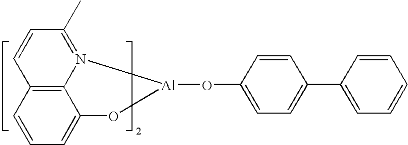 |
US20060202194 | |
 |
WO2005014551 | |
| Metal phenoxybenzothiazole compounds |
 |
Appl. Phys. Lett. 90, 123509 (2007) |
| Conjugated oligomers and polymers (e.g., polyfluorene) |
 |
Org. Electron. 1, 15 (2000) |
| Green hosts | ||
| Arylcarbazoles |
 |
Appl. Phys. Lett. 78, 1622 (2001) |
 |
US2003175553 | |
 |
WO2001039234 | |
| Aryltriphenylene compounds |
 |
US20060280965 |
 |
US20060280965 | |
| Polymers (e.g., PVK) |
 |
Appl. Phys. Lett. 77, 2280 (2000) |
| Spirofluorene compounds |
 |
WO2004093207 |
| Metal phenoxybenzooxazole compounds |
 |
WO05089025 |
 |
WO06132173 | |
 |
JP200511610 | |
| Spirofluorene-carbazole compounds |
 |
JP2007254297 |
 |
JP2007254297 | |
| Indolocabazoles |
 |
WO07063796 |
 |
WO07063754 | |
| 5-member ring electron deficient heterocycles (e.g., triazole, oxadiazole) |
 |
J. Appl. Phys. 90, 5048 (2001) |
 |
WO04107822 | |
| Metal phenoxypyridine compounds |
 |
WO05030900 |
| Blue hosts | ||
| Arylcarbazoles |
 |
Appl. Phys. Lett, 82, 2422 (2003) |
 |
US20070190359 | |
| Dibenzothiophene- carbazole compounds |
 |
WO2006114966 |
| Phosphorescent dopants | ||
| Red dopants | ||
| Heavy metal porphyrins (e.g., PtOEP) |
 |
Nature 395, 151 (1998) |
| Iridium(III) organometallic complexes |
 |
Appl. Phys. Lett. 78, 1622 (2001) |
 |
US06835469 | |
 |
US06835469 | |
 |
US20060202194 | |
 |
US20060202194 | |
 |
US07087321 | |
 |
US07087321 | |
 |
Adv. Mater. 19, 739 (2007) | |
| Platinum(II) organometallic complexes |
 |
WO2003040257 |
| Osminum(III) complexes |
 |
Chem. Mater. 17, 3532 (2005) |
| Ruthenium(II) complexes |
 |
Adv. Mater. 17, 1059 (2005) |
| Green dopants | ||
| Iridium(III) organometallic complexes |
 |
Inorg. Chem. 40, 1704 (2001) |
 |
US2002034656 | |
 |
US06687266 | |
 |
Chem. Mater. 16, 2480 (2004) | |
 |
US2007190359 | |
 |
US 2006008670 JP2007123392 | |
 |
Adv. Mater. 16, 2003 (2004) | |
 |
Angew. Chem. Int. Ed. 2006, 45, 7800 | |
| Pt(II) organometallic complexes |
 |
Appl. Phys. Lett. 86, 153505 (2005) |
 |
Appl. Phys. Lett. 86, 153505 (2005) | |
 |
Chem. Lett. 34, 592 (2005) | |
| Gold complexes |
 |
Chem. Commun. 2906 (2005) |
| Rhenium(III) complexes |
 |
Inorg. Chem. 42, 1248 (2003) |
| Blue dopants | ||
| Iridium(III) organometallic complexes |
 |
WO2002002714 |
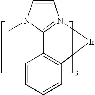 |
WO2006009024 | |
 |
US2006251923 | |
 |
WO2006056418, US2005260441 | |
 |
US2007190359 | |
 |
US2002134984 | |
 |
Angew. Chem. Int. Ed. 47, 1 (2008) | |
 |
Chem. Mater. 18, 5119 (2006) | |
 |
Inorg. Chem. 46, 4308 (2007) | |
 |
WO05123873 | |
 |
WO05123873 | |
 |
WO07004380 | |
 |
WO06082742 | |
| Osmium(II) complexes |
 |
US2005260449 |
 |
Organometallics 23, 3745 (2004) | |
| Gold complexes |
 |
Appl. Phys. Lett. 74, 1361 (1999) |
| Platinum(II) complexes |
 |
WO06098120, WO06103874 |
| Exciton/hole blocking layer materials |
| Bathocuprine compounds (e.g., BCP, BPhen) |
 |
Appl. Phys. Lett. 75, 4 (1999) |
 |
Appl. Phys. Lett. 79, 449 (2001) | |
| Metal 8-hydroxyquinolates (e.g., BAlq) |
 |
Appl. Phys. Lett. 81, 162 (2002) |
| 5-member ring electron dificient heterocycles such as triazole, oxadiazole, imidazole, benzoimidazole |
 |
Appl. Phys. Lett. 81, 162 (2002) |
| Triphenylene compounds |
 |
US20050025993 |
| Fluorinated aromatic compounds |
 |
Appl. Phys. Lett. 79, 156 (2001) |
| Electron transporting materials |
| Anthracene- benzoimidazole compounds |
 |
WO03060956 |
| Anthracene-benzothiazole compounds |
 |
Appl. Phys. Lett. 89, 063504 (2006) |
| Metal 8-hydroxyquinolates (e.g., Alq3) |
 |
Appl. Phys. Lett. 51, 913 (1987) |
| Metal hydroxybenoquinolates |
 |
Chem. Lett. 5, 905 (1993) |
| Bathocuprine compounds such as BCP, BPhen, etc |
 |
Appl. Phys. Lett. 91. 263503 (2007) |
 |
Appl. Phys. Lett. 79, 449 (2001) | |
| 5-member ring electron deficient heterocycles (e.g., triazole, oxadiazole, imidazole, benzoimidazole) |
 |
Appl. Phys. Lett. 74, 865 (1999) |
 |
Appl. Phys. Lett. 55, 1489 (1989) | |
 |
Jpn. J. Apply. Phys. 32, L917 (1993) | |
| Silole compounds |
 |
Org. Electron. 4, 113 (2003) |
| Arylborane compounds |
 |
J. Am. Chem. Soc. 120, 9714 (1998) |
| Fluorinated aromatic compounds |
 |
J. Am. Chem. Soc. 122, 1832 (2000) |


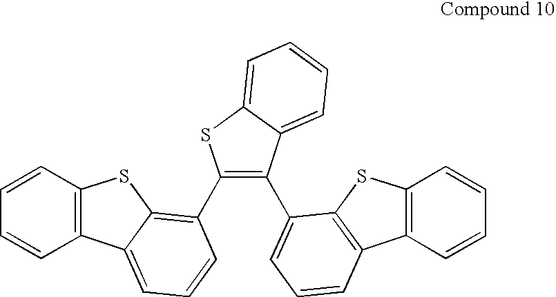


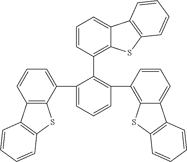


| TABLE 2 | |||||
| ITO | |||||
| Device | Dopant | thickness | |||
| Example | Host | wt % | ETL2 (Å) | ETL1 (Å) | (Å) |
| Comparative 1 | | P1 | 10% | HPT (50) | Alq3 (450) | 1200 |
| 1 | Cmpd 1 | |
Cmpd 1 | Alq3 (400) | 1200 | |
| (100) | ||||||
| 2 | Cmpd 1 | |
Cmpd 1 | Alq3 (400) | 1200 | |
| (100) | ||||||
| 3 | Cmpd 1 | |
HPT (50) | Alq3 (450) | 1200 | |
| 4 | Cmpd 1 | |
HPT (50) | Alq3 (450) | 1200 | |
| 5 | |
|
HPT (50) | Alq3 (400) | 800 | |
| 6 | |
|
HPT (50) | Alq3 (400) | 800 | |
| 7 | |
|
HPT (50) | Alq3 (400) | 1200 | |
| 8 | |
|
HPT (50) | Alq3 (400) | 1200 | |
| TABLE 3 | |||
| At J = | |||
| At L = 1000 cd/m2 | 40 mA/cm2 | ||
| Device | CIE | Emission | FWHM | LE | EQE | PE | L0 | LT80% |
| Example | X | Y | max (nm) | (nm) | V (V) | (cd/A) | (%) | (lm/W) | (cd/m2) | (hr) |
| Comparative 1 | 0.346 | 0.613 | 522 | 75 | 6.2 | 57.0 | 16 | 28.9 | 13,304 | 105 |
| 1 | 0.337 | 0.619 | 523 | 73 | 7.4 | 48.2 | 13 | 20.5 | 13,611 | 325 |
| 2 | 0.328 | 0.620 | 520 | 73 | 7.4 | 36.8 | 10 | 15.6 | 12,284 | 340 |
| 3 | 0.338 | 0.618 | 524 | 73 | 6.3 | 60.3 | 17 | 30.1 | 13,683 | 300 |
| 4 | 0.328 | 0.621 | 520 | 73 | 6.4 | 52 | 14.4 | 25.5 | 14,014 | 187 |
| 5 | 0.336 | 0.623 | 524 | 72 | 5.9 | 53.8 | 15 | 28.7 | 16389 | 18 |
| 6 | 0.349 | 0.614 | 528 | 73 | 6.1 | 45.5 | 12 | 23.2 | 15672 | 28 |
| 7 | 0.355 | 0.609 | 528 | 74 | 6.8 | 39.6 | 11 | 18.3 | 13403 | 98 |
| 8 | 0.353 | 0.613 | 528 | 72 | 6.3 | 49.5 | 14 | 24.7 | 15442 | 5.5 |
| TABLE 4 | ||||||
| Device | Anode | HIL | EML1 | EML2 | ETL2 | ETL1 |
| 9 | ITO | LG101 | Cmpd 1: | Cmpd 1: P3 (18%) | none | LG201 |
| [1200 Å] | [100 Å] | P4 (30%):P5 (0.5%) [300 Å] | [250 Å] | [300 Å] | ||
| 10 | ITO | LG101 | Cmpd 1: | Cmpd 1: P3 (12%) | none | LG201 |
| [1200 Å] | [100 Å] | P4 (30%):P5 (0.5%) [300 Å] | [250 Å] | [300 Å] | ||
| 11 | ITO | LG101 | Cmpd 1: | Cmpd 1: P3 (24%) | none | LG201 |
| [1200 Å] | [100 Å] | P4 (30%):P5 (0.5%) [300 Å] | [250 Å] | [300 Å] | ||
| 12 | ITO | LG101 | Cmpd 1: | Cmpd 1: P3 (24%) | Cmpd 1 [50 Å] | LG201 |
| [1200 Å] | [100 Å] | P4 (30%):P5 (0.5%) [300 Å] | [250 Å] | [300 Å] | ||
| 13 | ITO | LG101 | Cmpd 1: | Cmpd 1: P3 (18%) | Cmpd 1 [50 Å] | LG201 |
| [1200 Å] | [100 Å] | P4 (30%):P5 (0.5%) [300 Å] | [250 Å] | [300 Å] | ||
| 14 | ITO | LG101 | Cmpd 1: | Cmpd 1: P3 (12%) | Cmpd 1 [50 Å] | LG201 |
| [1200 Å] | [100 Å] | P4 (30%):P5 (0.5%) [300 Å] | [250 Å] | [300 Å] | ||
| 15 | ITO | LG101 | Cmpd 1: | Cmpd 1: P3 (18%) | Cmpd 1 [50 Å] | LG201 |
| [1200 Å] | [200 Å] | P4 (30%):P5 (0.5%) [200 Å] | [250 Å] | [300 Å] | ||
| 16 | ITO | LG101 | Cmpd 1: | Cmpd 1: P3 (18%) | Cmpd 1 [50 Å] | LG201 |
| [1200 Å] | [100 Å] | P4 (30%):P5 (0.5%) [200 Å] | [250 Å] | [300 Å] | ||
| TABLE 5 | ||||
| At 1,000 cd/m2 | At 10 | |||
| V | LE | EQE | PE | mA/cm2 | At L0 = 1,000 cd/m2 |
| Device | (V) | (cd/A) | (%) | (lm/W) | CIE x | CIE y | LT70% (hr) | LT60% (hr) |
| 9 | 6.1 | 23.7 | 10.9 | 12.3 | 0.467 | 0.457 | Not measured | Not measured |
| 10 | 6.2 | 31.7 | 15.1 | 16.1 | 0.500 | 0.445 | 35,500 | 100,000 |
| 11 | 6.2 | 14.9 | 6.9 | 7.5 | 0.467 | 0.457 | Not measured | Not measured |
| 12 | 6.1 | 29.5 | 13.5 | 15.2 | 0.456 | 0.460 | 78,000 | 140,000 |
| 13 | 6.3 | 32.4 | 15.3 | 16.1 | 0.437 | 0.451 | 90,000 | 230,000 |
| 14 | 7.0 | 33.2 | 16.3 | 15.0 | 0.505 | 0.439 | 88,000 | 180,000 |
| 15 | 6.4 | 29.0 | 13.9 | 14.3 | 0.472 | 0.449 | Not measured | Not measured |
| 16 | 6.2 | 29.4 | 14.2 | 14.9 | 0.467 | 0.448 | Not measured | Not measured |
| TABLE 6 | |||
| At 1000 cd/m2 | At 40 mA/cm2 | ||
| Device | Host | Dopant | ETL2 | ETL1 | CIE | V | L.E. | EQE | PE | L0 | LT80% |
| example | Cmpd | x % | (Å) | (Å) | X | Y | (V) | (cd/A) | (%) | (lm/W) | (cd/m2) | (hr) |
| 17 | 23 | P1 10% | 23 | Alq3 | 0.355 | 0.605 | 7.1 | 42.2 | 11.7 | 18.66 | 13,580 | 160 |
| (100 Å) | (400 Å) | |||||||||||
| 18 | 23 | P1 15% | 23 | Alq3 | 0.353 | 0.609 | 6.8 | 42.1 | 11.6 | 19.44 | 14,521 | 155 |
| (100 Å) | (450 Å) | |||||||||||
| 19 | 23 | P1 1% | HPT | Alq3 | 0.355 | 0.607 | 6.8 | 46.9 | 13 | 21.66 | 14,728 | 94 |
| (50 Å) | (450 Å) | |||||||||||
| 20 | 23 | P1 15% | HPT | Alq3 | 0.352 | 0.611 | 6.6 | 44.9 | 12.3 | 21.36 | 15,070 | 63 |
| (50 Å) | (400 Å) | |||||||||||
| TABLE 7 | ||||||
| Device | Anode | HIL | HTL | EML | ETL2 | ETL1 |
| 21 | ITO | LG101 | none | H1: |
H1 [250 Å] | Alq3 |
| [800 Å] | [100 Å] | [200 Å] | ||||
| 22 | ITO | LG101 | NPD | H1: |
H1 [50 Å] | Alq3 |
| [2000 Å] | [100 Å] | [300 Å] | [400 Å] | |||
| 23 | ITO | P1[100 Å] | NPD | H1: |
H1 [50 Å] | Alq3 |
| [800 Å] | [300 Å] | [400 Å] | ||||
| 24 | Sapphire/IZO | LG101 | none | H1: |
H1 [150 Å] | Alq3 |
| [800 Å] | [100 Å] | [300 Å] | ||||
| TABLE 8 | ||||
| At L0 = | ||||
| At 1000 cd/m2 | At 10 | 1000 | ||
| V | LE | EQE | PE | mA/cm2 | cd/m2 |
| Device | (V) | (cd/A) | (%) | (lm/W) | CIE x | CIE y | LT80% (hr) |
| 21 | 12.9 | 10.0 | 5.3 | 2.4 | 0.160 | 0.285 | 352 |
| 22 | 7.6 | 10.9 | 6.6 | 4.5 | 0.155 | 0.234 | 77 |
| 23 | 9.0 | 12.1 | 6.0 | 4.2 | 0.162 | 0.317 | 151 |
| 24 | 7.1 | 8.9 | 5.5 | 4.0 | 0.145 | 0.232 | 205 |
Claims (12)


Priority Applications (7)
| Application Number | Priority Date | Filing Date | Title |
|---|---|---|---|
| US12/208,907 US8007927B2 (en) | 2007-12-28 | 2008-09-11 | Dibenzothiophene-containing materials in phosphorescent light emitting diodes |
| US12/869,284 US8586204B2 (en) | 2007-12-28 | 2010-08-26 | Phosphorescent emitters and host materials with improved stability |
| US13/186,204 US8580402B2 (en) | 2007-12-28 | 2011-07-19 | Dibenzothiophene-containing materials in phosphorescent light emitting diodes |
| US14/026,868 US9123903B2 (en) | 2007-12-28 | 2013-09-13 | Dibenzothiophene-containing materials in phosphorescent light emitting diodes |
| US14/054,239 US20140042413A1 (en) | 2007-12-28 | 2013-10-15 | Phosphorescent emitters and host materials with improved stability |
| US14/802,051 US9997726B2 (en) | 2007-12-28 | 2015-07-17 | Dibenzothiophene-containing materials in phosphorescent light emitting diodes |
| US15/395,470 US9735377B2 (en) | 2005-05-06 | 2016-12-30 | Phosphorescent emitters and host materials with improved stability |
Applications Claiming Priority (2)
| Application Number | Priority Date | Filing Date | Title |
|---|---|---|---|
| US1748007P | 2007-12-28 | 2007-12-28 | |
| US12/208,907 US8007927B2 (en) | 2007-12-28 | 2008-09-11 | Dibenzothiophene-containing materials in phosphorescent light emitting diodes |
Related Parent Applications (1)
| Application Number | Title | Priority Date | Filing Date |
|---|---|---|---|
| US14/713,615 Continuation-In-Part US10381579B2 (en) | 2005-05-06 | 2015-05-15 | Stability OLED materials and devices |
Related Child Applications (2)
| Application Number | Title | Priority Date | Filing Date |
|---|---|---|---|
| US12/869,284 Continuation-In-Part US8586204B2 (en) | 2005-05-06 | 2010-08-26 | Phosphorescent emitters and host materials with improved stability |
| US13/186,204 Division US8580402B2 (en) | 2007-12-28 | 2011-07-19 | Dibenzothiophene-containing materials in phosphorescent light emitting diodes |
Publications (2)
| Publication Number | Publication Date |
|---|---|
| US20090167162A1 US20090167162A1 (en) | 2009-07-02 |
| US8007927B2 true US8007927B2 (en) | 2011-08-30 |
Family
ID=40689327
Family Applications (4)
| Application Number | Title | Priority Date | Filing Date |
|---|---|---|---|
| US12/208,907 Active 2029-06-02 US8007927B2 (en) | 2005-05-06 | 2008-09-11 | Dibenzothiophene-containing materials in phosphorescent light emitting diodes |
| US13/186,204 Active US8580402B2 (en) | 2007-12-28 | 2011-07-19 | Dibenzothiophene-containing materials in phosphorescent light emitting diodes |
| US14/026,868 Active 2029-02-19 US9123903B2 (en) | 2007-12-28 | 2013-09-13 | Dibenzothiophene-containing materials in phosphorescent light emitting diodes |
| US14/802,051 Active 2029-06-24 US9997726B2 (en) | 2007-12-28 | 2015-07-17 | Dibenzothiophene-containing materials in phosphorescent light emitting diodes |
Family Applications After (3)
| Application Number | Title | Priority Date | Filing Date |
|---|---|---|---|
| US13/186,204 Active US8580402B2 (en) | 2007-12-28 | 2011-07-19 | Dibenzothiophene-containing materials in phosphorescent light emitting diodes |
| US14/026,868 Active 2029-02-19 US9123903B2 (en) | 2007-12-28 | 2013-09-13 | Dibenzothiophene-containing materials in phosphorescent light emitting diodes |
| US14/802,051 Active 2029-06-24 US9997726B2 (en) | 2007-12-28 | 2015-07-17 | Dibenzothiophene-containing materials in phosphorescent light emitting diodes |
Country Status (3)
| Country | Link |
|---|---|
| US (4) | US8007927B2 (en) |
| TW (3) | TWI554506B (en) |
| WO (1) | WO2009085344A2 (en) |
Cited By (21)
| Publication number | Priority date | Publication date | Assignee | Title |
|---|---|---|---|---|
| US20100141126A1 (en) * | 2007-05-16 | 2010-06-10 | Konica Minolta Holdings, Inc. | Organic electroluminescent element, display and illuminating device |
| US20100301383A1 (en) * | 2009-05-29 | 2010-12-02 | Semiconductor Energy Laboratory Co., Ltd. | Light-Emitting Element, Light-Emitting Device, and Method for Manufacturing the Same |
| US20100301382A1 (en) * | 2009-05-29 | 2010-12-02 | Semiconductor Energy Laboratory Co., Ltd. | Light-Emitting Element, Light-Emitting Device, Lighting Device, and Electronic Appliance |
| US20120049165A1 (en) * | 2010-08-31 | 2012-03-01 | National Tsing Hua University | Organic light emitting diode and manufacturing method thereof |
| US20130002132A1 (en) * | 2010-01-20 | 2013-01-03 | Universal Display Corporation | Electroluminescent devices for lighting applications |
| US8993125B2 (en) | 2010-05-21 | 2015-03-31 | Semiconductor Energy Laboratory Co., Ltd. | Triazole derivative, and light-emitting element, light-emitting device, electronic device and lighting device using the triazole derivative |
| US9065058B2 (en) | 2010-09-10 | 2015-06-23 | Semiconductor Energy Laboratory Co., Ltd. | Light-emitting element and electronic device |
| US9123903B2 (en) | 2007-12-28 | 2015-09-01 | Universal Display Corporation | Dibenzothiophene-containing materials in phosphorescent light emitting diodes |
| US9309223B2 (en) | 2011-07-08 | 2016-04-12 | Semiconductor Energy Laboratory Co., Ltd. | Heterocyclic compound, light-emitting element, light-emitting device, electronic device, and lighting device |
| US9406889B2 (en) | 2010-10-29 | 2016-08-02 | Semiconductor Energy Laboratory Co., Ltd. | Phenanthrene compound, light-emitting element, light-emitting device, electronic device, and lighting device |
| US9406893B2 (en) | 2010-09-09 | 2016-08-02 | Semiconductor Energy Laboratory Co., Ltd. | Heterocyclic compound, light-emitting element, light-emitting device, electronic device, and lighting device |
| US9496505B2 (en) | 2010-10-04 | 2016-11-15 | Semiconductor Energy Laboratory Co., Ltd. | Composite material, light-emitting element, light-emitting device, electronic device, and lighting device |
| US9799834B2 (en) | 2011-08-18 | 2017-10-24 | Semiconductor Energy Laboratory Co., Ltd. | Carbazole compound light-emitting element, light-emitting device, electronic device, and lighting device |
| US9831435B2 (en) | 2011-03-23 | 2017-11-28 | Semiconductor Energy Laboratory Co., Ltd. | Composite material, light-emitting element, light-emitting device, electronic device, and lighting device |
| US9905782B2 (en) | 2013-03-26 | 2018-02-27 | Semiconductor Energy Laboratory Co., Ltd. | Light-emitting element, compound, organic compound, display module, lighting module, light-emitting device, display device, lighting device, and electronic device |
| US9960368B2 (en) | 2011-02-01 | 2018-05-01 | Semiconductor Energy Laboratory Co., Ltd. | Heterocyclic compound |
| US10017691B2 (en) | 2007-05-16 | 2018-07-10 | Konica Minolta, Inc. | Organic electroluminescent element, display device and lighting device |
| US10071993B2 (en) | 2010-09-21 | 2018-09-11 | Semiconductor Energy Laboratory Co., Ltd. | Carbazole derivative, light-emitting element material and organic semiconductor material |
| US10424745B2 (en) | 2009-11-02 | 2019-09-24 | Semiconductor Energy Laboratory Co., Ltd. | Organometallic complex, light-emitting element, display device, electronic device, and lighting device |
| US10586931B2 (en) | 2015-12-25 | 2020-03-10 | Semiconductor Energy Laboratory Co., Ltd. | Compound, light-emitting element, display device, electronic device, and lighting device |
| US11107995B2 (en) | 2016-06-24 | 2021-08-31 | Semiconductor Energy Laboratory Co., Ltd. | Organic compound, light-emitting element, light-emitting device, electronic device, and lighting device |
Families Citing this family (572)
| Publication number | Priority date | Publication date | Assignee | Title |
|---|---|---|---|---|
| US8128753B2 (en) | 2004-11-19 | 2012-03-06 | Massachusetts Institute Of Technology | Method and apparatus for depositing LED organic film |
| US8986780B2 (en) | 2004-11-19 | 2015-03-24 | Massachusetts Institute Of Technology | Method and apparatus for depositing LED organic film |
| US9070884B2 (en) | 2005-04-13 | 2015-06-30 | Universal Display Corporation | Hybrid OLED having phosphorescent and fluorescent emitters |
| US9051344B2 (en) | 2005-05-06 | 2015-06-09 | Universal Display Corporation | Stability OLED materials and devices |
| US8586204B2 (en) * | 2007-12-28 | 2013-11-19 | Universal Display Corporation | Phosphorescent emitters and host materials with improved stability |
| CN101415718B (en) | 2006-02-10 | 2013-05-29 | 通用显示公司 | Metal complexes of cyclometallated imidazo[1,2-f]phenanthridine and diimidazo[1,2-a:1',2'-c]quinazoline ligands and isoelectronic and benzannulated analogs thereof |
| US8778508B2 (en) | 2006-12-08 | 2014-07-15 | Universal Display Corporation | Light-emitting organometallic complexes |
| US20130032785A1 (en) | 2011-08-01 | 2013-02-07 | Universal Display Corporation | Materials for organic light emitting diode |
| US9130177B2 (en) | 2011-01-13 | 2015-09-08 | Universal Display Corporation | 5-substituted 2 phenylquinoline complexes materials for light emitting diode |
| KR102413285B1 (en) | 2007-03-08 | 2022-06-28 | 유니버셜 디스플레이 코포레이션 | Phosphorescent materials |
| US8556389B2 (en) | 2011-02-04 | 2013-10-15 | Kateeva, Inc. | Low-profile MEMS thermal printhead die having backside electrical connections |
| WO2008157420A2 (en) * | 2007-06-14 | 2008-12-24 | Massachusetts Institute Of Technology | Method and apparatus for thermal jet printing |
| CN103601609B (en) | 2007-08-08 | 2017-07-28 | 通用显示公司 | The luxuriant and rich with fragrance chromophore of single benzo [9,10] in phosphorescent light emitting diode |
| TWI531567B (en) | 2007-08-08 | 2016-05-01 | 環球展覽公司 | Organic electroluminescent materials and devices |
| EP2288671B1 (en) * | 2008-06-10 | 2012-08-15 | Basf Se | Novel transition metal complex and use thereof in organic light-emitting diodes - iii |
| US8632145B2 (en) | 2008-06-13 | 2014-01-21 | Kateeva, Inc. | Method and apparatus for printing using a facetted drum |
| US10434804B2 (en) | 2008-06-13 | 2019-10-08 | Kateeva, Inc. | Low particle gas enclosure systems and methods |
| US8899171B2 (en) | 2008-06-13 | 2014-12-02 | Kateeva, Inc. | Gas enclosure assembly and system |
| US9048344B2 (en) | 2008-06-13 | 2015-06-02 | Kateeva, Inc. | Gas enclosure assembly and system |
| US8383202B2 (en) | 2008-06-13 | 2013-02-26 | Kateeva, Inc. | Method and apparatus for load-locked printing |
| US9604245B2 (en) | 2008-06-13 | 2017-03-28 | Kateeva, Inc. | Gas enclosure systems and methods utilizing an auxiliary enclosure |
| CN102131767B (en) | 2008-06-30 | 2013-08-21 | 通用显示公司 | Hole transport materials containing triphenylene |
| WO2010027583A1 (en) | 2008-09-03 | 2010-03-11 | Universal Display Corporation | Phosphorescent materials |
| TWI555734B (en) | 2008-09-16 | 2016-11-01 | 環球展覽公司 | Phosphorescent materials |
| KR101678235B1 (en) | 2008-09-25 | 2016-11-21 | 유니버셜 디스플레이 코포레이션 | Organoselenium materials and their uses in organic light emitting devices |
| KR101919207B1 (en) * | 2008-11-11 | 2018-11-15 | 유니버셜 디스플레이 코포레이션 | Phosphorescent emitters |
| US8815415B2 (en) | 2008-12-12 | 2014-08-26 | Universal Display Corporation | Blue emitter with high efficiency based on imidazo[1,2-f] phenanthridine iridium complexes |
| US20100188457A1 (en) * | 2009-01-05 | 2010-07-29 | Madigan Connor F | Method and apparatus for controlling the temperature of an electrically-heated discharge nozzle |
| KR100994118B1 (en) * | 2009-01-13 | 2010-11-15 | 삼성모바일디스플레이주식회사 | Organic light emitting diode and manufacturing method thereof |
| US9067947B2 (en) * | 2009-01-16 | 2015-06-30 | Universal Display Corporation | Organic electroluminescent materials and devices |
| US8722205B2 (en) | 2009-03-23 | 2014-05-13 | Universal Display Corporation | Heteroleptic iridium complex |
| US8709615B2 (en) | 2011-07-28 | 2014-04-29 | Universal Display Corporation | Heteroleptic iridium complexes as dopants |
| US11910700B2 (en) | 2009-03-23 | 2024-02-20 | Universal Display Corporation | Heteroleptic iridium complexes as dopants |
| TWI687408B (en) | 2009-04-28 | 2020-03-11 | 美商環球展覽公司 | Iridium complex with methyl-D3 substitution |
| WO2010127328A2 (en) * | 2009-05-01 | 2010-11-04 | Kateeva, Inc. | Method and apparatus for organic vapor printing |
| US8586203B2 (en) | 2009-05-20 | 2013-11-19 | Universal Display Corporation | Metal complexes with boron-nitrogen heterocycle containing ligands |
| US8545996B2 (en) | 2009-11-02 | 2013-10-01 | The University Of Southern California | Ion-pairing soft salts based on organometallic complexes and their applications in organic light emitting diodes |
| US8580394B2 (en) | 2009-11-19 | 2013-11-12 | Universal Display Corporation | 3-coordinate copper(I)-carbene complexes |
| US9156870B2 (en) * | 2010-02-25 | 2015-10-13 | Universal Display Corporation | Phosphorescent emitters |
| US9175211B2 (en) * | 2010-03-03 | 2015-11-03 | Universal Display Corporation | Phosphorescent materials |
| WO2011119162A1 (en) | 2010-03-25 | 2011-09-29 | Universal Display Corporation | Solution processable doped triarylamine hole injection materials |
| CN102823016A (en) * | 2010-03-31 | 2012-12-12 | 出光兴产株式会社 | Material for organic electroluminescent element and organic electroluminescent element using same |
| KR101181261B1 (en) | 2010-04-21 | 2012-09-10 | 덕산하이메탈(주) | Compound Containing Dibenzothiophene, Arylamine Derivatives And Organic Electronic Element Using The Same, Terminal Thereof |
| US8968887B2 (en) | 2010-04-28 | 2015-03-03 | Universal Display Corporation | Triphenylene-benzofuran/benzothiophene/benzoselenophene compounds with substituents joining to form fused rings |
| CN103026521B (en) | 2010-04-28 | 2016-11-09 | 通用显示公司 | The material of deposition premixing |
| KR20110122051A (en) | 2010-05-03 | 2011-11-09 | 제일모직주식회사 | Compound for organic photoelectric device and organic photoelectric device including the same |
| JP2013200939A (en) | 2010-06-08 | 2013-10-03 | Idemitsu Kosan Co Ltd | Organic electroluminescent element |
| US8742657B2 (en) | 2010-06-11 | 2014-06-03 | Universal Display Corporation | Triplet-Triplet annihilation up conversion (TTA-UC) for display and lighting applications |
| US8673458B2 (en) | 2010-06-11 | 2014-03-18 | Universal Display Corporation | Delayed fluorescence OLED |
| CN101935523A (en) * | 2010-07-13 | 2011-01-05 | 西安瑞联近代电子材料有限责任公司 | Novel efficient metallic iridium coordination compound red organic electrophosphorescent material and organic electroluminescent device thereof |
| CN101899296A (en) * | 2010-07-13 | 2010-12-01 | 西安瑞联近代电子材料有限责任公司 | Red organic electroluminescent phosphorescent material containing aryl united quinazoline metal iridium complexes and organic electroluminescent device thereof |
| WO2012016074A1 (en) | 2010-07-29 | 2012-02-02 | University Of Southern California | Co-deposition methods for the fabrication of organic optoelectronic devices |
| JP5763309B2 (en) * | 2010-07-30 | 2015-08-12 | ユー・ディー・シー アイルランド リミテッド | Organic electroluminescent device and compound |
| TWI480279B (en) * | 2010-08-16 | 2015-04-11 | Novel carbazole derivatives and organic light emitting diode devices for their applications | |
| KR102004629B1 (en) | 2010-08-20 | 2019-07-26 | 유니버셜 디스플레이 코포레이션 | Bicarbazole compounds for oleds |
| EP2428512B1 (en) * | 2010-09-08 | 2014-10-22 | Semiconductor Energy Laboratory Co., Ltd. | Fluorene compound, light-emitting element, light-emitting device, electronic device and lighting device |
| JP5847420B2 (en) * | 2010-09-08 | 2016-01-20 | ユー・ディー・シー アイルランド リミテッド | Organic electroluminescent device and compound |
| JP5729957B2 (en) * | 2010-09-29 | 2015-06-03 | キヤノン株式会社 | Dibenzothiophene compound and organic light emitting device having the same |
| US8932734B2 (en) | 2010-10-08 | 2015-01-13 | Universal Display Corporation | Organic electroluminescent materials and devices |
| US9133173B2 (en) * | 2010-10-15 | 2015-09-15 | Semiconductor Energy Laboratory Co., Ltd. | Carbazole compound, material for light-emitting element, organic semiconductor material, light-emitting element |
| TWI431003B (en) | 2010-10-21 | 2014-03-21 | Ind Tech Res Inst | Organic compound and organic electroluminescence device employing the same |
| US8269317B2 (en) | 2010-11-11 | 2012-09-18 | Universal Display Corporation | Phosphorescent materials |
| KR101531612B1 (en) | 2010-12-02 | 2015-06-25 | 제일모직 주식회사 | Compound for organic photoelectric device and organic photoelectric device including the same |
| US20120138906A1 (en) | 2010-12-07 | 2012-06-07 | The University of Southern California USC Stevens Institute for Innovation | Capture agents for unsaturated metal complexes |
| US10008677B2 (en) | 2011-01-13 | 2018-06-26 | Universal Display Corporation | Materials for organic light emitting diode |
| US8415031B2 (en) | 2011-01-24 | 2013-04-09 | Universal Display Corporation | Electron transporting compounds |
| JP2012153628A (en) * | 2011-01-25 | 2012-08-16 | Canon Inc | Dibenzothiophene dioxide compound and organic light-emitting device using the same |
| US9005772B2 (en) | 2011-02-23 | 2015-04-14 | Universal Display Corporation | Thioazole and oxazole carbene metal complexes as phosphorescent OLED materials |
| US8563737B2 (en) | 2011-02-23 | 2013-10-22 | Universal Display Corporation | Methods of making bis-tridentate carbene complexes of ruthenium and osmium |
| TWI644918B (en) | 2011-02-23 | 2018-12-21 | Universal Display Corporation | Novel tetradentate platinum complexes |
| US8748011B2 (en) | 2011-02-23 | 2014-06-10 | Universal Display Corporation | Ruthenium carbene complexes for OLED material |
| US8492006B2 (en) | 2011-02-24 | 2013-07-23 | Universal Display Corporation | Germanium-containing red emitter materials for organic light emitting diode |
| US8883322B2 (en) | 2011-03-08 | 2014-11-11 | Universal Display Corporation | Pyridyl carbene phosphorescent emitters |
| JP5984450B2 (en) | 2011-03-31 | 2016-09-06 | ユー・ディー・シー アイルランド リミテッド | ORGANIC ELECTROLUMINESCENT ELEMENT, LIGHT EMITTING DEVICE USING THE ELEMENT, DISPLAY DEVICE, LIGHTING DEVICE, AND COMPOUND FOR THE ELEMENT |
| US8580399B2 (en) * | 2011-04-08 | 2013-11-12 | Universal Display Corporation | Substituted oligoazacarbazoles for light emitting diodes |
| US8927308B2 (en) | 2011-05-12 | 2015-01-06 | Universal Display Corporation | Method of forming bus line designs for large-area OLED lighting |
| US8432095B2 (en) | 2011-05-11 | 2013-04-30 | Universal Display Corporation | Process for fabricating metal bus lines for OLED lighting panels |
| US8564192B2 (en) | 2011-05-11 | 2013-10-22 | Universal Display Corporation | Process for fabricating OLED lighting panels |
| US9212197B2 (en) | 2011-05-19 | 2015-12-15 | Universal Display Corporation | Phosphorescent heteroleptic phenylbenzimidazole dopants |
| US8795850B2 (en) | 2011-05-19 | 2014-08-05 | Universal Display Corporation | Phosphorescent heteroleptic phenylbenzimidazole dopants and new synthetic methodology |
| KR101559431B1 (en) * | 2011-05-20 | 2015-10-15 | 주식회사 엠비케이 | Organic light compound and organic light device using the same |
| US8748012B2 (en) | 2011-05-25 | 2014-06-10 | Universal Display Corporation | Host materials for OLED |
| US10079349B2 (en) | 2011-05-27 | 2018-09-18 | Universal Display Corporation | Organic electroluminescent materials and devices |
| US10158089B2 (en) | 2011-05-27 | 2018-12-18 | Universal Display Corporation | Organic electroluminescent materials and devices |
| KR102119353B1 (en) | 2011-06-08 | 2020-06-29 | 유니버셜 디스플레이 코포레이션 | Heteroleptic iridium carbene complexes and light emitting device using them |
| US8659036B2 (en) | 2011-06-17 | 2014-02-25 | Universal Display Corporation | Fine tuning of emission spectra by combination of multiple emitter spectra |
| US8884316B2 (en) | 2011-06-17 | 2014-11-11 | Universal Display Corporation | Non-common capping layer on an organic device |
| KR101965014B1 (en) | 2011-07-14 | 2019-04-02 | 유니버셜 디스플레이 코포레이션 | Inorganic hosts in oleds |
| US9023420B2 (en) | 2011-07-14 | 2015-05-05 | Universal Display Corporation | Composite organic/inorganic layer for organic light-emitting devices |
| US9397310B2 (en) | 2011-07-14 | 2016-07-19 | Universal Display Corporation | Organice electroluminescent materials and devices |
| US9783564B2 (en) | 2011-07-25 | 2017-10-10 | Universal Display Corporation | Organic electroluminescent materials and devices |
| US8409729B2 (en) | 2011-07-28 | 2013-04-02 | Universal Display Corporation | Host materials for phosphorescent OLEDs |
| US8926119B2 (en) | 2011-08-04 | 2015-01-06 | Universal Display Corporation | Extendable light source with variable light emitting area |
| US8552420B2 (en) | 2011-08-09 | 2013-10-08 | Universal Display Corporation | OLED light panel with controlled brightness variation |
| US9493698B2 (en) | 2011-08-31 | 2016-11-15 | Universal Display Corporation | Organic electroluminescent materials and devices |
| WO2013038843A1 (en) * | 2011-09-12 | 2013-03-21 | 新日鉄住金化学株式会社 | Organic electroluminescent element |
| US8652656B2 (en) | 2011-11-14 | 2014-02-18 | Universal Display Corporation | Triphenylene silane hosts |
| JP2013103918A (en) | 2011-11-15 | 2013-05-30 | Udc Ireland Ltd | Charge-transporting material, organic electroluminescent element, and light-emitting device, display device and illumination device characterized by using the element |
| US9193745B2 (en) | 2011-11-15 | 2015-11-24 | Universal Display Corporation | Heteroleptic iridium complex |
| US9217004B2 (en) | 2011-11-21 | 2015-12-22 | Universal Display Corporation | Organic light emitting materials |
| US9512355B2 (en) | 2011-12-09 | 2016-12-06 | Universal Display Corporation | Organic light emitting materials |
| US20130146875A1 (en) | 2011-12-13 | 2013-06-13 | Universal Display Corporation | Split electrode for organic devices |
| WO2013094834A1 (en) * | 2011-12-19 | 2013-06-27 | 율촌화학 주식회사 | Novel compound having stability, and charge transfer material and blue phosphorescent organic light emitting diode comprising same |
| US8987451B2 (en) | 2012-01-03 | 2015-03-24 | Universal Display Corporation | Synthesis of cyclometallated platinum(II) complexes |
| US9461254B2 (en) | 2012-01-03 | 2016-10-04 | Universal Display Corporation | Organic electroluminescent materials and devices |
| US9163174B2 (en) | 2012-01-04 | 2015-10-20 | Universal Display Corporation | Highly efficient phosphorescent materials |
| KR102012047B1 (en) | 2012-01-06 | 2019-08-19 | 유니버셜 디스플레이 코포레이션 | Highly efficient phosphorescent materials |
| US8969592B2 (en) | 2012-01-10 | 2015-03-03 | Universal Display Corporation | Heterocyclic host materials |
| US10211413B2 (en) | 2012-01-17 | 2019-02-19 | Universal Display Corporation | Organic electroluminescent materials and devices |
| US9118017B2 (en) | 2012-02-27 | 2015-08-25 | Universal Display Corporation | Host compounds for red phosphorescent OLEDs |
| US9386657B2 (en) | 2012-03-15 | 2016-07-05 | Universal Display Corporation | Organic Electroluminescent materials and devices |
| US9054323B2 (en) | 2012-03-15 | 2015-06-09 | Universal Display Corporation | Secondary hole transporting layer with diarylamino-phenyl-carbazole compounds |
| US8723209B2 (en) | 2012-04-27 | 2014-05-13 | Universal Display Corporation | Out coupling layer containing particle polymer composite |
| US9184399B2 (en) | 2012-05-04 | 2015-11-10 | Universal Display Corporation | Asymmetric hosts with triaryl silane side chains |
| WO2013172835A1 (en) * | 2012-05-17 | 2013-11-21 | Universal Display Corporation | Biscarbazole derivative host materials for oled emissive region |
| US9773985B2 (en) | 2012-05-21 | 2017-09-26 | Universal Display Corporation | Organic electroluminescent materials and devices |
| JP5182441B1 (en) * | 2012-05-24 | 2013-04-17 | 三菱化学株式会社 | Organic electroluminescent device, organic electroluminescent lighting device and organic electroluminescent display device |
| US9670404B2 (en) | 2012-06-06 | 2017-06-06 | Universal Display Corporation | Organic electroluminescent materials and devices |
| JP6100368B2 (en) * | 2012-06-14 | 2017-03-22 | ユニバーサル ディスプレイ コーポレイション | Biscarbazole derivative host material and green light emitter for OLED light emitting region |
| US9502672B2 (en) | 2012-06-21 | 2016-11-22 | Universal Display Corporation | Organic electroluminescent materials and devices |
| US9725476B2 (en) | 2012-07-09 | 2017-08-08 | Universal Display Corporation | Silylated metal complexes |
| US9231218B2 (en) | 2012-07-10 | 2016-01-05 | Universal Display Corporation | Phosphorescent emitters containing dibenzo[1,4]azaborinine structure |
| US9540329B2 (en) | 2012-07-19 | 2017-01-10 | Universal Display Corporation | Organic electroluminescent materials and devices |
| US9059412B2 (en) | 2012-07-19 | 2015-06-16 | Universal Display Corporation | Transition metal complexes containing substituted imidazole carbene as ligands and their application in OLEDs |
| US9663544B2 (en) | 2012-07-25 | 2017-05-30 | Universal Display Corporation | Organic electroluminescent materials and devices |
| US9318710B2 (en) | 2012-07-30 | 2016-04-19 | Universal Display Corporation | Organic electroluminescent materials and devices |
| US9978958B2 (en) | 2012-08-24 | 2018-05-22 | Universal Display Corporation | Phosphorescent emitters with phenylimidazole ligands |
| US8952362B2 (en) | 2012-08-31 | 2015-02-10 | The Regents Of The University Of Michigan | High efficiency and brightness fluorescent organic light emitting diode by triplet-triplet fusion |
| US10957870B2 (en) | 2012-09-07 | 2021-03-23 | Universal Display Corporation | Organic light emitting device |
| US9287513B2 (en) | 2012-09-24 | 2016-03-15 | Universal Display Corporation | Organic electroluminescent materials and devices |
| US9312505B2 (en) | 2012-09-25 | 2016-04-12 | Universal Display Corporation | Organic electroluminescent materials and devices |
| JP6194645B2 (en) | 2012-09-27 | 2017-09-13 | 東ソー株式会社 | Amine compounds and uses thereof |
| US9252363B2 (en) | 2012-10-04 | 2016-02-02 | Universal Display Corporation | Aryloxyalkylcarboxylate solvent compositions for inkjet printing of organic layers |
| US8692241B1 (en) | 2012-11-08 | 2014-04-08 | Universal Display Corporation | Transition metal complexes containing triazole and tetrazole carbene ligands |
| US9634264B2 (en) | 2012-11-09 | 2017-04-25 | Universal Display Corporation | Organic electroluminescent materials and devices |
| US8946697B1 (en) | 2012-11-09 | 2015-02-03 | Universal Display Corporation | Iridium complexes with aza-benzo fused ligands |
| US9748500B2 (en) | 2015-01-15 | 2017-08-29 | Universal Display Corporation | Organic light emitting materials |
| US9685617B2 (en) | 2012-11-09 | 2017-06-20 | Universal Display Corporation | Organic electronuminescent materials and devices |
| US10069090B2 (en) | 2012-11-20 | 2018-09-04 | Universal Display Corporation | Organic electroluminescent materials and devices |
| US9190623B2 (en) | 2012-11-20 | 2015-11-17 | Universal Display Corporation | Organic electroluminescent materials and devices |
| US9512136B2 (en) | 2012-11-26 | 2016-12-06 | Universal Display Corporation | Organic electroluminescent materials and devices |
| US9166175B2 (en) | 2012-11-27 | 2015-10-20 | Universal Display Corporation | Organic electroluminescent materials and devices |
| US9196860B2 (en) | 2012-12-04 | 2015-11-24 | Universal Display Corporation | Compounds for triplet-triplet annihilation upconversion |
| US8716484B1 (en) | 2012-12-05 | 2014-05-06 | Universal Display Corporation | Hole transporting materials with twisted aryl groups |
| US9209411B2 (en) | 2012-12-07 | 2015-12-08 | Universal Display Corporation | Organic electroluminescent materials and devices |
| US9653691B2 (en) | 2012-12-12 | 2017-05-16 | Universal Display Corporation | Phosphorescence-sensitizing fluorescence material system |
| KR102160720B1 (en) * | 2012-12-17 | 2020-09-28 | 닛테츠 케미컬 앤드 머티리얼 가부시키가이샤 | Organic electrical field light-emitting element |
| US20140203259A1 (en) * | 2013-01-18 | 2014-07-24 | Universal Display Corporation | Host for organic light emitting devices |
| US10400163B2 (en) | 2013-02-08 | 2019-09-03 | Universal Display Corporation | Organic electroluminescent materials and devices |
| US10367154B2 (en) | 2013-02-21 | 2019-07-30 | Universal Display Corporation | Organic electroluminescent materials and devices |
| US8927749B2 (en) | 2013-03-07 | 2015-01-06 | Universal Display Corporation | Organic electroluminescent materials and devices |
| US9419225B2 (en) | 2013-03-14 | 2016-08-16 | Universal Display Corporation | Organic electroluminescent materials and devices |
| US9997712B2 (en) | 2013-03-27 | 2018-06-12 | Universal Display Corporation | Organic electroluminescent materials and devices |
| US9537106B2 (en) | 2013-05-09 | 2017-01-03 | Universal Display Corporation | Organic electroluminescent materials and devices |
| US9735373B2 (en) | 2013-06-10 | 2017-08-15 | Universal Display Corporation | Organic electroluminescent materials and devices |
| US9673401B2 (en) | 2013-06-28 | 2017-06-06 | Universal Display Corporation | Organic electroluminescent materials and devices |
| US10199581B2 (en) | 2013-07-01 | 2019-02-05 | Universal Display Corporation | Organic electroluminescent materials and devices |
| US10121975B2 (en) | 2013-07-03 | 2018-11-06 | Universal Display Corporation | Organic electroluminescent materials and devices |
| CN104277063B (en) * | 2013-07-07 | 2019-02-01 | 潘才法 | A kind of compound based on borazine and the application in organic electronic device |
| US9761807B2 (en) | 2013-07-15 | 2017-09-12 | Universal Display Corporation | Organic light emitting diode materials |
| US9553274B2 (en) | 2013-07-16 | 2017-01-24 | Universal Display Corporation | Organic electroluminescent materials and devices |
| US9324949B2 (en) | 2013-07-16 | 2016-04-26 | Universal Display Corporation | Organic electroluminescent materials and devices |
| TWI633100B (en) | 2013-07-19 | 2018-08-21 | 半導體能源研究所股份有限公司 | Organic compound, light-emitting element, display module, lighting module, light-emitting device, display device, lighting device, and electronic device |
| US9224958B2 (en) | 2013-07-19 | 2015-12-29 | Universal Display Corporation | Organic electroluminescent materials and devices |
| US20150028290A1 (en) | 2013-07-25 | 2015-01-29 | Universal Display Corporation | Heteroleptic osmium complex and method of making the same |
| US10074806B2 (en) | 2013-08-20 | 2018-09-11 | Universal Display Corporation | Organic electroluminescent materials and devices |
| US9831437B2 (en) | 2013-08-20 | 2017-11-28 | Universal Display Corporation | Organic electroluminescent materials and devices |
| US9932359B2 (en) | 2013-08-30 | 2018-04-03 | University Of Southern California | Organic electroluminescent materials and devices |
| US10199582B2 (en) | 2013-09-03 | 2019-02-05 | University Of Southern California | Organic electroluminescent materials and devices |
| US9735378B2 (en) | 2013-09-09 | 2017-08-15 | Universal Display Corporation | Organic electroluminescent materials and devices |
| US9748503B2 (en) | 2013-09-13 | 2017-08-29 | Universal Display Corporation | Organic electroluminescent materials and devices |
| US10003034B2 (en) | 2013-09-30 | 2018-06-19 | Universal Display Corporation | Organic electroluminescent materials and devices |
| US9831447B2 (en) | 2013-10-08 | 2017-11-28 | Universal Display Corporation | Organic electroluminescent materials and devices |
| US9293712B2 (en) | 2013-10-11 | 2016-03-22 | Universal Display Corporation | Disubstituted pyrene compounds with amino group containing ortho aryl group and devices containing the same |
| US9853229B2 (en) | 2013-10-23 | 2017-12-26 | University Of Southern California | Organic electroluminescent materials and devices |
| US20150115250A1 (en) | 2013-10-29 | 2015-04-30 | Universal Display Corporation | Organic electroluminescent materials and devices |
| US9306179B2 (en) | 2013-11-08 | 2016-04-05 | Universal Display Corporation | Organic electroluminescent materials and devices |
| US9647218B2 (en) | 2013-11-14 | 2017-05-09 | Universal Display Corporation | Organic electroluminescent materials and devices |
| US10033000B2 (en) | 2013-11-15 | 2018-07-24 | Universal Display Corporation | Organic electroluminescent materials and devices |
| US10056565B2 (en) | 2013-11-20 | 2018-08-21 | Universal Display Corporation | Organic electroluminescent materials and devices |
| US10644251B2 (en) | 2013-12-04 | 2020-05-05 | Universal Display Corporation | Organic electroluminescent materials and devices |
| US9876173B2 (en) | 2013-12-09 | 2018-01-23 | Universal Display Corporation | Organic electroluminescent materials and devices |
| US10355227B2 (en) | 2013-12-16 | 2019-07-16 | Universal Display Corporation | Metal complex for phosphorescent OLED |
| US9847496B2 (en) | 2013-12-23 | 2017-12-19 | Universal Display Corporation | Organic electroluminescent materials and devices |
| CN105794011B (en) | 2013-12-26 | 2017-07-21 | 新日铁住金化学株式会社 | Organic electric-field light-emitting element material and use its organic electric-field light-emitting element |
| EP3787016B1 (en) | 2013-12-26 | 2023-09-20 | Kateeva, Inc. | Apparatus and techniques for thermal treatment of electronic devices |
| US10283721B2 (en) * | 2013-12-26 | 2019-05-07 | Nippon Steel Chemical & Material Co., Ltd. | Material for organic electroluminescent elements, and organic electroluminescent element using same |
| US10135008B2 (en) | 2014-01-07 | 2018-11-20 | Universal Display Corporation | Organic electroluminescent materials and devices |
| US9978961B2 (en) | 2014-01-08 | 2018-05-22 | Universal Display Corporation | Organic electroluminescent materials and devices |
| EP3624175B1 (en) | 2014-01-21 | 2021-12-22 | Kateeva, Inc. | Method for electronic device encapsulation |
| US9755159B2 (en) | 2014-01-23 | 2017-09-05 | Universal Display Corporation | Organic materials for OLEDs |
| US9935277B2 (en) | 2014-01-30 | 2018-04-03 | Universal Display Corporation | Organic electroluminescent materials and devices |
| US9590194B2 (en) | 2014-02-14 | 2017-03-07 | Universal Display Corporation | Organic electroluminescent materials and devices |
| US10003033B2 (en) | 2014-02-18 | 2018-06-19 | Universal Display Corporation | Organic electroluminescent materials and devices |
| US9847497B2 (en) | 2014-02-18 | 2017-12-19 | Universal Display Corporation | Organic electroluminescent materials and devices |
| US10707423B2 (en) | 2014-02-21 | 2020-07-07 | Universal Display Corporation | Organic electroluminescent materials and devices |
| US9647217B2 (en) | 2014-02-24 | 2017-05-09 | Universal Display Corporation | Organic electroluminescent materials and devices |
| US9502656B2 (en) | 2014-02-24 | 2016-11-22 | Universal Display Corporation | Organic electroluminescent materials and devices |
| US10403825B2 (en) | 2014-02-27 | 2019-09-03 | Universal Display Corporation | Organic electroluminescent materials and devices |
| US9590195B2 (en) | 2014-02-28 | 2017-03-07 | Universal Display Corporation | Organic electroluminescent materials and devices |
| US9673407B2 (en) | 2014-02-28 | 2017-06-06 | Universal Display Corporation | Organic electroluminescent materials and devices |
| US9181270B2 (en) | 2014-02-28 | 2015-11-10 | Universal Display Corporation | Method of making sulfide compounds |
| US9190620B2 (en) | 2014-03-01 | 2015-11-17 | Universal Display Corporation | Organic electroluminescent materials and devices |
| US10497883B2 (en) * | 2014-03-11 | 2019-12-03 | Kyulux, Inc. | Organic light-emitting device, host material, light-emitting material, and compound |
| US9397309B2 (en) | 2014-03-13 | 2016-07-19 | Universal Display Corporation | Organic electroluminescent devices |
| US10208026B2 (en) | 2014-03-18 | 2019-02-19 | Universal Display Corporation | Organic electroluminescent materials and devices |
| US10529932B2 (en) | 2014-03-24 | 2020-01-07 | Nippon Steel Chemical & Material Co., Ltd. | Organic-electroluminescent-element material and organic electroluminescent element using same |
| EP3125326B1 (en) | 2014-03-24 | 2018-08-29 | Nippon Steel & Sumikin Chemical Co., Ltd. | Organic-electroluminescent-element material and organic electroluminescent elements using same |
| US9748504B2 (en) | 2014-03-25 | 2017-08-29 | Universal Display Corporation | Organic electroluminescent materials and devices |
| US9929353B2 (en) | 2014-04-02 | 2018-03-27 | Universal Display Corporation | Organic electroluminescent materials and devices |
| US9691993B2 (en) | 2014-04-09 | 2017-06-27 | Universal Display Corporation | Organic electroluminescent materials and devices |
| US10008679B2 (en) | 2014-04-14 | 2018-06-26 | Universal Display Corporation | Organic electroluminescent materials and devices |
| US9847498B2 (en) | 2014-04-14 | 2017-12-19 | Universal Display Corporation | Organic electroluminescent materials and devices |
| US10256427B2 (en) | 2014-04-15 | 2019-04-09 | Universal Display Corporation | Efficient organic electroluminescent devices |
| US9450198B2 (en) | 2014-04-15 | 2016-09-20 | Universal Display Corporation | Organic electroluminescent materials and devices |
| JP6307332B2 (en) * | 2014-04-21 | 2018-04-04 | 新日鉄住金化学株式会社 | Organic electroluminescence device |
| US9741941B2 (en) | 2014-04-29 | 2017-08-22 | Universal Display Corporation | Organic electroluminescent materials and devices |
| KR102177898B1 (en) | 2014-04-30 | 2020-11-12 | 카티바, 인크. | Gas cushion apparatus and techniques for substrate coating |
| US10457699B2 (en) | 2014-05-02 | 2019-10-29 | Universal Display Corporation | Organic electroluminescent materials and devices |
| EP3741768B1 (en) | 2014-05-08 | 2022-12-07 | Universal Display Corporation | Stabilized imidazophenanthridine materials |
| US10301338B2 (en) | 2014-05-08 | 2019-05-28 | Universal Display Corporation | Organic electroluminescent materials and devices |
| US10636983B2 (en) | 2014-05-08 | 2020-04-28 | Universal Display Corporation | Organic electroluminescent materials and devices |
| US10403830B2 (en) | 2014-05-08 | 2019-09-03 | Universal Display Corporation | Organic electroluminescent materials and devices |
| US9997716B2 (en) | 2014-05-27 | 2018-06-12 | Universal Display Corporation | Organic electroluminescent materials and devices |
| US10461260B2 (en) | 2014-06-03 | 2019-10-29 | Universal Display Corporation | Organic electroluminescent materials and devices |
| US9911931B2 (en) | 2014-06-26 | 2018-03-06 | Universal Display Corporation | Organic electroluminescent materials and devices |
| US10297762B2 (en) | 2014-07-09 | 2019-05-21 | Universal Display Corporation | Organic electroluminescent materials and devices |
| US10566546B2 (en) | 2014-07-14 | 2020-02-18 | Universal Display Corporation | Organic electroluminescent materials and devices |
| US9929357B2 (en) | 2014-07-22 | 2018-03-27 | Universal Display Corporation | Organic electroluminescent materials and devices |
| US10411200B2 (en) | 2014-08-07 | 2019-09-10 | Universal Display Corporation | Electroluminescent (2-phenylpyridine)iridium complexes and devices |
| US11108000B2 (en) | 2014-08-07 | 2021-08-31 | Unniversal Display Corporation | Organic electroluminescent materials and devices |
| KR101733151B1 (en) * | 2014-08-21 | 2017-05-08 | 삼성디스플레이 주식회사 | Organic light emitting diode and organic light emitting display device including the same |
| US10135007B2 (en) | 2014-09-29 | 2018-11-20 | Universal Display Corporation | Organic electroluminescent materials and devices |
| JP6383623B2 (en) * | 2014-09-29 | 2018-08-29 | 新日鉄住金化学株式会社 | Organic electroluminescence device |
| US10043987B2 (en) | 2014-09-29 | 2018-08-07 | Universal Display Corporation | Organic electroluminescent materials and devices |
| US10749113B2 (en) | 2014-09-29 | 2020-08-18 | Universal Display Corporation | Organic electroluminescent materials and devices |
| US10361375B2 (en) | 2014-10-06 | 2019-07-23 | Universal Display Corporation | Organic electroluminescent materials and devices |
| US9397302B2 (en) | 2014-10-08 | 2016-07-19 | Universal Display Corporation | Organic electroluminescent materials and devices |
| US10854826B2 (en) | 2014-10-08 | 2020-12-01 | Universal Display Corporation | Organic electroluminescent compounds, compositions and devices |
| US10950803B2 (en) | 2014-10-13 | 2021-03-16 | Universal Display Corporation | Compounds and uses in devices |
| US9484541B2 (en) | 2014-10-20 | 2016-11-01 | Universal Display Corporation | Organic electroluminescent materials and devices |
| US10868261B2 (en) | 2014-11-10 | 2020-12-15 | Universal Display Corporation | Organic electroluminescent materials and devices |
| US10038151B2 (en) | 2014-11-12 | 2018-07-31 | Universal Display Corporation | Organic electroluminescent materials and devices |
| US10411201B2 (en) | 2014-11-12 | 2019-09-10 | Universal Display Corporation | Organic electroluminescent materials and devices |
| US9882151B2 (en) | 2014-11-14 | 2018-01-30 | Universal Display Corporation | Organic electroluminescent materials and devices |
| US9871212B2 (en) | 2014-11-14 | 2018-01-16 | Universal Display Corporation | Organic electroluminescent materials and devices |
| US9761814B2 (en) | 2014-11-18 | 2017-09-12 | Universal Display Corporation | Organic light-emitting materials and devices |
| US9444075B2 (en) | 2014-11-26 | 2016-09-13 | Universal Display Corporation | Emissive display with photo-switchable polarization |
| US9450195B2 (en) | 2014-12-17 | 2016-09-20 | Universal Display Corporation | Organic electroluminescent materials and devices |
| US10253252B2 (en) | 2014-12-30 | 2019-04-09 | Universal Display Corporation | Organic electroluminescent materials and devices |
| US10636978B2 (en) | 2014-12-30 | 2020-04-28 | Universal Display Corporation | Organic electroluminescent materials and devices |
| US9312499B1 (en) | 2015-01-05 | 2016-04-12 | Universal Display Corporation | Organic electroluminescent materials and devices |
| US9406892B2 (en) | 2015-01-07 | 2016-08-02 | Universal Display Corporation | Organic electroluminescent materials and devices |
| US10418569B2 (en) | 2015-01-25 | 2019-09-17 | Universal Display Corporation | Organic electroluminescent materials and devices |
| US9711730B2 (en) | 2015-01-25 | 2017-07-18 | Universal Display Corporation | Organic electroluminescent materials and devices |
| US10418562B2 (en) | 2015-02-06 | 2019-09-17 | Universal Display Corporation | Organic electroluminescent materials and devices |
| US10644247B2 (en) | 2015-02-06 | 2020-05-05 | Universal Display Corporation | Organic electroluminescent materials and devices |
| US10355222B2 (en) | 2015-02-06 | 2019-07-16 | Universal Display Corporation | Organic electroluminescent materials and devices |
| US10177316B2 (en) | 2015-02-09 | 2019-01-08 | Universal Display Corporation | Organic electroluminescent materials and devices |
| US10144867B2 (en) | 2015-02-13 | 2018-12-04 | Universal Display Corporation | Organic electroluminescent materials and devices |
| US10680183B2 (en) | 2015-02-15 | 2020-06-09 | Universal Display Corporation | Organic electroluminescent materials and devices |
| US9929361B2 (en) | 2015-02-16 | 2018-03-27 | Universal Display Corporation | Organic electroluminescent materials and devices |
| US10600966B2 (en) | 2015-02-27 | 2020-03-24 | Universal Display Corporation | Organic electroluminescent materials and devices |
| US11056657B2 (en) | 2015-02-27 | 2021-07-06 | University Display Corporation | Organic electroluminescent materials and devices |
| US10686143B2 (en) | 2015-03-05 | 2020-06-16 | Universal Display Corporation | Organic electroluminescent materials and devices |
| US10270046B2 (en) | 2015-03-06 | 2019-04-23 | Universal Display Corporation | Organic electroluminescent materials and devices |
| US9780316B2 (en) | 2015-03-16 | 2017-10-03 | Universal Display Corporation | Organic electroluminescent materials and devices |
| US9911928B2 (en) | 2015-03-19 | 2018-03-06 | Universal Display Corporation | Organic electroluminescent materials and devices |
| US9871214B2 (en) | 2015-03-23 | 2018-01-16 | Universal Display Corporation | Organic electroluminescent materials and devices |
| US10529931B2 (en) | 2015-03-24 | 2020-01-07 | Universal Display Corporation | Organic Electroluminescent materials and devices |
| US10297770B2 (en) | 2015-03-27 | 2019-05-21 | Universal Display Corporation | Organic electroluminescent materials and devices |
| US11495749B2 (en) | 2015-04-06 | 2022-11-08 | Universal Display Corporation | Organic electroluminescent materials and devices |
| US10593890B2 (en) | 2015-04-06 | 2020-03-17 | Universal Display Corporation | Organic electroluminescent materials and devices |
| US11818949B2 (en) | 2015-04-06 | 2023-11-14 | Universal Display Corporation | Organic electroluminescent materials and devices |
| KR101910112B1 (en) * | 2015-05-06 | 2018-10-19 | 삼성에스디아이 주식회사 | Dopant for organic optoelectronic device and organic optoelectronic device and display device |
| US10777749B2 (en) | 2015-05-07 | 2020-09-15 | Universal Display Corporation | Organic electroluminescent materials and devices |
| US10403826B2 (en) | 2015-05-07 | 2019-09-03 | Universal Display Corporation | Organic electroluminescent materials and devices |
| US9478758B1 (en) | 2015-05-08 | 2016-10-25 | Universal Display Corporation | Organic electroluminescent materials and devices |
| US9859510B2 (en) | 2015-05-15 | 2018-01-02 | Universal Display Corporation | Organic electroluminescent materials and devices |
| US10256411B2 (en) | 2015-05-21 | 2019-04-09 | Universal Display Corporation | Organic electroluminescent materials and devices |
| US10109799B2 (en) | 2015-05-21 | 2018-10-23 | Universal Display Corporation | Organic electroluminescent materials and devices |
| WO2016193845A1 (en) | 2015-05-29 | 2016-12-08 | Semiconductor Energy Laboratory Co., Ltd. | Light-emitting element, light-emitting device, display device, electronic device, and lighting device |
| US10033004B2 (en) | 2015-06-01 | 2018-07-24 | Universal Display Corporation | Organic electroluminescent materials and devices |
| US10418568B2 (en) | 2015-06-01 | 2019-09-17 | Universal Display Corporation | Organic electroluminescent materials and devices |
| US11925102B2 (en) | 2015-06-04 | 2024-03-05 | Universal Display Corporation | Organic electroluminescent materials and devices |
| US10825997B2 (en) | 2015-06-25 | 2020-11-03 | Universal Display Corporation | Organic electroluminescent materials and devices |
| US10873036B2 (en) | 2015-07-07 | 2020-12-22 | Universal Display Corporation | Organic electroluminescent materials and devices |
| US9978956B2 (en) | 2015-07-15 | 2018-05-22 | Universal Display Corporation | Organic electroluminescent materials and devices |
| US11127905B2 (en) | 2015-07-29 | 2021-09-21 | Universal Display Corporation | Organic electroluminescent materials and devices |
| US11018309B2 (en) | 2015-08-03 | 2021-05-25 | Universal Display Corporation | Organic electroluminescent materials and devices |
| US11522140B2 (en) | 2015-08-17 | 2022-12-06 | Universal Display Corporation | Organic electroluminescent materials and devices |
| US10522769B2 (en) | 2015-08-18 | 2019-12-31 | Universal Display Corporation | Organic electroluminescent materials and devices |
| US10181564B2 (en) | 2015-08-26 | 2019-01-15 | Universal Display Corporation | Organic electroluminescent materials and devices |
| US10672996B2 (en) | 2015-09-03 | 2020-06-02 | Universal Display Corporation | Organic electroluminescent materials and devices |
| US11706972B2 (en) | 2015-09-08 | 2023-07-18 | Universal Display Corporation | Organic electroluminescent materials and devices |
| US11302872B2 (en) | 2015-09-09 | 2022-04-12 | Universal Display Corporation | Organic electroluminescent materials and devices |
| US10770664B2 (en) | 2015-09-21 | 2020-09-08 | Universal Display Corporation | Organic electroluminescent materials and devices |
| US20170092880A1 (en) | 2015-09-25 | 2017-03-30 | Universal Display Corporation | Organic electroluminescent materials and devices |
| US10593892B2 (en) | 2015-10-01 | 2020-03-17 | Universal Display Corporation | Organic electroluminescent materials and devices |
| US10847728B2 (en) | 2015-10-01 | 2020-11-24 | Universal Display Corporation | Organic electroluminescent materials and devices |
| US10991895B2 (en) | 2015-10-06 | 2021-04-27 | Universal Display Corporation | Organic electroluminescent materials and devices |
| US10388892B2 (en) | 2015-10-29 | 2019-08-20 | Universal Display Corporation | Organic electroluminescent materials and devices |
| US10177318B2 (en) | 2015-10-29 | 2019-01-08 | Universal Display Corporation | Organic electroluminescent materials and devices |
| US10388893B2 (en) | 2015-10-29 | 2019-08-20 | Universal Display Corporation | Organic electroluminescent materials and devices |
| CN108350352B (en) * | 2015-11-02 | 2021-03-30 | 默克专利有限公司 | Material for organic electroluminescent device |
| US10998507B2 (en) | 2015-11-23 | 2021-05-04 | Universal Display Corporation | Organic electroluminescent materials and devices |
| US10476010B2 (en) | 2015-11-30 | 2019-11-12 | Universal Display Corporation | Organic electroluminescent materials and devices |
| US10957861B2 (en) | 2015-12-29 | 2021-03-23 | Universal Display Corporation | Organic electroluminescent materials and devices |
| US11024808B2 (en) | 2015-12-29 | 2021-06-01 | Universal Display Corporation | Organic electroluminescent materials and devices |
| US10135006B2 (en) | 2016-01-04 | 2018-11-20 | Universal Display Corporation | Organic electroluminescent materials and devices |
| US20170229663A1 (en) | 2016-02-09 | 2017-08-10 | Universal Display Corporation | Organic electroluminescent materials and devices |
| US10707427B2 (en) | 2016-02-09 | 2020-07-07 | Universal Display Corporation | Organic electroluminescent materials and devices |
| US10457864B2 (en) | 2016-02-09 | 2019-10-29 | Universal Display Corporation | Organic electroluminescent materials and devices |
| US10600967B2 (en) | 2016-02-18 | 2020-03-24 | Universal Display Corporation | Organic electroluminescent materials and devices |
| US11094891B2 (en) | 2016-03-16 | 2021-08-17 | Universal Display Corporation | Organic electroluminescent materials and devices |
| CN108886105A (en) | 2016-03-28 | 2018-11-23 | 新日铁住金化学株式会社 | Organic electric-field light-emitting element |
| US10276809B2 (en) | 2016-04-05 | 2019-04-30 | Universal Display Corporation | Organic electroluminescent materials and devices |
| US10236456B2 (en) | 2016-04-11 | 2019-03-19 | Universal Display Corporation | Organic electroluminescent materials and devices |
| US10566552B2 (en) | 2016-04-13 | 2020-02-18 | Universal Display Corporation | Organic electroluminescent materials and devices |
| US11228003B2 (en) | 2016-04-22 | 2022-01-18 | Universal Display Corporation | Organic electroluminescent materials and devices |
| US11228002B2 (en) | 2016-04-22 | 2022-01-18 | Universal Display Corporation | Organic electroluminescent materials and devices |
| US11081647B2 (en) | 2016-04-22 | 2021-08-03 | Universal Display Corporation | Organic electroluminescent materials and devices |
| US10840458B2 (en) | 2016-05-25 | 2020-11-17 | Universal Display Corporation | Organic electroluminescent materials and devices |
| KR102018682B1 (en) * | 2016-05-26 | 2019-09-04 | 덕산네오룩스 주식회사 | Compound for organic electronic element, organic electronic element using the same, and an electronic device thereof |
| US10468609B2 (en) | 2016-06-02 | 2019-11-05 | Universal Display Corporation | Organic electroluminescent materials and devices |
| US10686140B2 (en) | 2016-06-20 | 2020-06-16 | Universal Display Corporation | Organic electroluminescent materials and devices |
| US10727423B2 (en) | 2016-06-20 | 2020-07-28 | Universal Display Corporation | Organic electroluminescent materials and devices |
| US10672997B2 (en) | 2016-06-20 | 2020-06-02 | Universal Display Corporation | Organic electroluminescent materials and devices |
| US10651403B2 (en) | 2016-06-20 | 2020-05-12 | Universal Display Corporation | Organic electroluminescent materials and devices |
| US10862054B2 (en) | 2016-06-20 | 2020-12-08 | Universal Display Corporation | Organic electroluminescent materials and devices |
| US11482683B2 (en) | 2016-06-20 | 2022-10-25 | Universal Display Corporation | Organic electroluminescent materials and devices |
| US10957866B2 (en) | 2016-06-30 | 2021-03-23 | Universal Display Corporation | Organic electroluminescent materials and devices |
| US9929360B2 (en) | 2016-07-08 | 2018-03-27 | Universal Display Corporation | Organic electroluminescent materials and devices |
| US10566547B2 (en) | 2016-07-11 | 2020-02-18 | Universal Display Corporation | Organic electroluminescent materials and devices |
| US10720587B2 (en) | 2016-07-19 | 2020-07-21 | Universal Display Corporation | Organic electroluminescent materials and devices |
| US10153443B2 (en) | 2016-07-19 | 2018-12-11 | Universal Display Corporation | Organic electroluminescent materials and devices |
| US10205105B2 (en) | 2016-08-15 | 2019-02-12 | Universal Display Corporation | Organic electroluminescent materials and devices |
| US10608186B2 (en) | 2016-09-14 | 2020-03-31 | Universal Display Corporation | Organic electroluminescent materials and devices |
| US10505127B2 (en) | 2016-09-19 | 2019-12-10 | Universal Display Corporation | Organic electroluminescent materials and devices |
| US10680187B2 (en) | 2016-09-23 | 2020-06-09 | Universal Display Corporation | Organic electroluminescent materials and devices |
| US11196010B2 (en) | 2016-10-03 | 2021-12-07 | Universal Display Corporation | Organic electroluminescent materials and devices |
| US11081658B2 (en) | 2016-10-03 | 2021-08-03 | Universal Display Corporation | Organic electroluminescent materials and devices |
| US11183642B2 (en) | 2016-10-03 | 2021-11-23 | Universal Display Corporation | Organic electroluminescent materials and devices |
| US11189804B2 (en) | 2016-10-03 | 2021-11-30 | Universal Display Corporation | Organic electroluminescent materials and devices |
| US11127906B2 (en) | 2016-10-03 | 2021-09-21 | Universal Display Corporation | Organic electroluminescent materials and devices |
| US11011709B2 (en) | 2016-10-07 | 2021-05-18 | Universal Display Corporation | Organic electroluminescent materials and devices |
| US11239432B2 (en) | 2016-10-14 | 2022-02-01 | Universal Display Corporation | Organic electroluminescent materials and devices |
| US10608185B2 (en) | 2016-10-17 | 2020-03-31 | Univeral Display Corporation | Organic electroluminescent materials and devices |
| US10236458B2 (en) | 2016-10-24 | 2019-03-19 | Universal Display Corporation | Organic electroluminescent materials and devices |
| US20180130956A1 (en) | 2016-11-09 | 2018-05-10 | Universal Display Corporation | Organic electroluminescent materials and devices |
| US10340464B2 (en) | 2016-11-10 | 2019-07-02 | Universal Display Corporation | Organic electroluminescent materials and devices |
| US10680188B2 (en) | 2016-11-11 | 2020-06-09 | Universal Display Corporation | Organic electroluminescent materials and devices |
| US10897016B2 (en) | 2016-11-14 | 2021-01-19 | Universal Display Corporation | Organic electroluminescent materials and devices |
| US10662196B2 (en) | 2016-11-17 | 2020-05-26 | Universal Display Corporation | Organic electroluminescent materials and devices |
| US10964893B2 (en) | 2016-11-17 | 2021-03-30 | Universal Display Corporation | Organic electroluminescent materials and devices |
| US10153445B2 (en) | 2016-11-21 | 2018-12-11 | Universal Display Corporation | Organic electroluminescent materials and devices |
| US10833276B2 (en) | 2016-11-21 | 2020-11-10 | Universal Display Corporation | Organic electroluminescent materials and devices |
| GB2556125A (en) * | 2016-11-22 | 2018-05-23 | Sumitomo Chemical Co | Method |
| US11555048B2 (en) | 2016-12-01 | 2023-01-17 | Universal Display Corporation | Organic electroluminescent materials and devices |
| US11548905B2 (en) | 2016-12-15 | 2023-01-10 | Universal Display Corporation | Organic electroluminescent materials and devices |
| US10490753B2 (en) | 2016-12-15 | 2019-11-26 | Universal Display Corporation | Organic electroluminescent materials and devices |
| US11545636B2 (en) | 2016-12-15 | 2023-01-03 | Universal Display Corporation | Organic electroluminescent materials and devices |
| US10811618B2 (en) | 2016-12-19 | 2020-10-20 | Universal Display Corporation | Organic electroluminescent materials and devices |
| KR101915716B1 (en) * | 2016-12-20 | 2018-11-08 | 희성소재 (주) | Organic light emitting device and composition for organic layer of organic light emitting device |
| US11152579B2 (en) | 2016-12-28 | 2021-10-19 | Universal Display Corporation | Organic electroluminescent materials and devices |
| US11780865B2 (en) | 2017-01-09 | 2023-10-10 | Universal Display Corporation | Organic electroluminescent materials and devices |
| US11201298B2 (en) | 2017-01-09 | 2021-12-14 | Universal Display Corporation | Organic electroluminescent materials and devices |
| US10804475B2 (en) | 2017-01-11 | 2020-10-13 | Universal Display Corporation | Organic electroluminescent materials and devices |
| US11545637B2 (en) | 2017-01-13 | 2023-01-03 | Universal Display Corporation | Organic electroluminescent materials and devices |
| US10629820B2 (en) | 2017-01-18 | 2020-04-21 | Universal Display Corporation | Organic electroluminescent materials and devices |
| US11053268B2 (en) | 2017-01-20 | 2021-07-06 | Universal Display Corporation | Organic electroluminescent materials and devices |
| US10964904B2 (en) | 2017-01-20 | 2021-03-30 | Universal Display Corporation | Organic electroluminescent materials and devices |
| US11765968B2 (en) | 2017-01-23 | 2023-09-19 | Universal Display Corporation | Organic electroluminescent materials and devices |
| US11050028B2 (en) | 2017-01-24 | 2021-06-29 | Universal Display Corporation | Organic electroluminescent materials and devices |
| US10978647B2 (en) | 2017-02-15 | 2021-04-13 | Universal Display Corporation | Organic electroluminescent materials and devices |
| US10822361B2 (en) | 2017-02-22 | 2020-11-03 | Universal Display Corporation | Organic electroluminescent materials and devices |
| US10745431B2 (en) | 2017-03-08 | 2020-08-18 | Universal Display Corporation | Organic electroluminescent materials and devices |
| US10741780B2 (en) | 2017-03-10 | 2020-08-11 | Universal Display Corporation | Organic electroluminescent materials and devices |
| US10672998B2 (en) | 2017-03-23 | 2020-06-02 | Universal Display Corporation | Organic electroluminescent materials and devices |
| US10873037B2 (en) | 2017-03-28 | 2020-12-22 | Universal Display Corporation | Organic electroluminescent materials and devices |
| US10910577B2 (en) | 2017-03-28 | 2021-02-02 | Universal Display Corporation | Organic electroluminescent materials and devices |
| US11158820B2 (en) | 2017-03-29 | 2021-10-26 | Universal Display Corporation | Organic electroluminescent materials and devices |
| US11056658B2 (en) | 2017-03-29 | 2021-07-06 | Universal Display Corporation | Organic electroluminescent materials and devices |
| US10844085B2 (en) | 2017-03-29 | 2020-11-24 | Universal Display Corporation | Organic electroluminescent materials and devices |
| US10862046B2 (en) | 2017-03-30 | 2020-12-08 | Universal Display Corporation | Organic electroluminescent materials and devices |
| US11276829B2 (en) | 2017-03-31 | 2022-03-15 | Universal Display Corporation | Organic electroluminescent materials and devices |
| US11139443B2 (en) | 2017-03-31 | 2021-10-05 | Universal Display Corporation | Organic electroluminescent materials and devices |
| US10777754B2 (en) | 2017-04-11 | 2020-09-15 | Universal Display Corporation | Organic electroluminescent materials and devices |
| US11038117B2 (en) | 2017-04-11 | 2021-06-15 | Universal Display Corporation | Organic electroluminescent materials and devices |
| US11084838B2 (en) | 2017-04-21 | 2021-08-10 | Universal Display Corporation | Organic electroluminescent materials and device |
| US11101434B2 (en) | 2017-04-21 | 2021-08-24 | Universal Display Corporation | Organic electroluminescent materials and devices |
| US10975113B2 (en) | 2017-04-21 | 2021-04-13 | Universal Display Corporation | Organic electroluminescent materials and devices |
| US10910570B2 (en) | 2017-04-28 | 2021-02-02 | Universal Display Corporation | Organic electroluminescent materials and devices |
| US11038137B2 (en) | 2017-04-28 | 2021-06-15 | Universal Display Corporation | Organic electroluminescent materials and devices |
| US11117897B2 (en) | 2017-05-01 | 2021-09-14 | Universal Display Corporation | Organic electroluminescent materials and devices |
| US10941170B2 (en) | 2017-05-03 | 2021-03-09 | Universal Display Corporation | Organic electroluminescent materials and devices |
| US10221153B2 (en) | 2017-05-03 | 2019-03-05 | Saint Louis University | Dibenzothiophene compounds |
| US11201299B2 (en) | 2017-05-04 | 2021-12-14 | Universal Display Corporation | Organic electroluminescent materials and devices |
| US10862055B2 (en) | 2017-05-05 | 2020-12-08 | Universal Display Corporation | Organic electroluminescent materials and devices |
| US10870668B2 (en) | 2017-05-05 | 2020-12-22 | Universal Display Corporation | Organic electroluminescent materials and devices |
| US10930864B2 (en) | 2017-05-10 | 2021-02-23 | Universal Display Corporation | Organic electroluminescent materials and devices |
| US10944060B2 (en) | 2017-05-11 | 2021-03-09 | Universal Display Corporation | Organic electroluminescent materials and devices |
| US10822362B2 (en) | 2017-05-11 | 2020-11-03 | Universal Display Corporation | Organic electroluminescent materials and devices |
| US10944062B2 (en) | 2017-05-18 | 2021-03-09 | Universal Display Corporation | Organic electroluminescent materials and devices |
| US10840459B2 (en) | 2017-05-18 | 2020-11-17 | Universal Display Corporation | Organic electroluminescent materials and devices |
| US10934293B2 (en) | 2017-05-18 | 2021-03-02 | Universal Display Corporation | Organic electroluminescent materials and devices |
| US10790455B2 (en) | 2017-05-18 | 2020-09-29 | Universal Display Corporation | Organic electroluminescent materials and devices |
| US11038115B2 (en) | 2017-05-18 | 2021-06-15 | Universal Display Corporation | Organic electroluminescent materials and device |
| US10930862B2 (en) | 2017-06-01 | 2021-02-23 | Universal Display Corporation | Organic electroluminescent materials and devices |
| US11814403B2 (en) | 2017-06-23 | 2023-11-14 | Universal Display Corporation | Organic electroluminescent materials and devices |
| US11832510B2 (en) | 2017-06-23 | 2023-11-28 | Universal Display Corporation | Organic electroluminescent materials and devices |
| US11802136B2 (en) | 2017-06-23 | 2023-10-31 | Universal Display Corporation | Organic electroluminescent materials and devices |
| US11608321B2 (en) | 2017-06-23 | 2023-03-21 | Universal Display Corporation | Organic electroluminescent materials and devices |
| US11495757B2 (en) | 2017-06-23 | 2022-11-08 | Universal Display Corporation | Organic electroluminescent materials and devices |
| US11552261B2 (en) | 2017-06-23 | 2023-01-10 | Universal Display Corporation | Organic electroluminescent materials and devices |
| US11678565B2 (en) | 2017-06-23 | 2023-06-13 | Universal Display Corporation | Organic electroluminescent materials and devices |
| US11758804B2 (en) | 2017-06-23 | 2023-09-12 | Universal Display Corporation | Organic electroluminescent materials and devices |
| US20180370999A1 (en) | 2017-06-23 | 2018-12-27 | Universal Display Corporation | Organic electroluminescent materials and devices |
| US11725022B2 (en) | 2017-06-23 | 2023-08-15 | Universal Display Corporation | Organic electroluminescent materials and devices |
| US11174259B2 (en) | 2017-06-23 | 2021-11-16 | Universal Display Corporation | Organic electroluminescent materials and devices |
| US10968226B2 (en) | 2017-06-23 | 2021-04-06 | Universal Display Corporation | Organic electroluminescent materials and devices |
| US11469382B2 (en) | 2017-07-12 | 2022-10-11 | Universal Display Corporation | Organic electroluminescent materials and devices |
| US11917843B2 (en) | 2017-07-26 | 2024-02-27 | Universal Display Corporation | Organic electroluminescent materials and devices |
| US11239433B2 (en) | 2017-07-26 | 2022-02-01 | Universal Display Corporation | Organic electroluminescent materials and devices |
| US11228010B2 (en) | 2017-07-26 | 2022-01-18 | Universal Display Corporation | Organic electroluminescent materials and devices |
| US11322691B2 (en) | 2017-07-26 | 2022-05-03 | Universal Display Corporation | Organic electroluminescent materials and devices |
| US11765970B2 (en) | 2017-07-26 | 2023-09-19 | Universal Display Corporation | Organic electroluminescent materials and devices |
| US11744141B2 (en) | 2017-08-09 | 2023-08-29 | Universal Display Corporation | Organic electroluminescent materials and devices |
| US11910699B2 (en) | 2017-08-10 | 2024-02-20 | Universal Display Corporation | Organic electroluminescent materials and devices |
| US11744142B2 (en) | 2017-08-10 | 2023-08-29 | Universal Display Corporation | Organic electroluminescent materials and devices |
| US11508913B2 (en) | 2017-08-10 | 2022-11-22 | Universal Display Corporation | Organic electroluminescent materials and devices |
| US11349083B2 (en) | 2017-08-10 | 2022-05-31 | Universal Display Corporation | Organic electroluminescent materials and devices |
| US11723269B2 (en) | 2017-08-22 | 2023-08-08 | Universal Display Corporation | Organic electroluminescent materials and devices |
| US11462697B2 (en) | 2017-08-22 | 2022-10-04 | Universal Display Corporation | Organic electroluminescent materials and devices |
| US11437591B2 (en) | 2017-08-24 | 2022-09-06 | Universal Display Corporation | Organic electroluminescent materials and devices |
| US11605791B2 (en) | 2017-09-01 | 2023-03-14 | Universal Display Corporation | Organic electroluminescent materials and devices |
| US11696492B2 (en) | 2017-09-07 | 2023-07-04 | Universal Display Corporation | Organic electroluminescent materials and devices |
| US11424420B2 (en) | 2017-09-07 | 2022-08-23 | Universal Display Corporation | Organic electroluminescent materials and devices |
| US11444249B2 (en) | 2017-09-07 | 2022-09-13 | Universal Display Corporation | Organic electroluminescent materials and devices |
| US10608188B2 (en) | 2017-09-11 | 2020-03-31 | Universal Display Corporation | Organic electroluminescent materials and devices |
| US11778897B2 (en) | 2017-09-20 | 2023-10-03 | Universal Display Corporation | Organic electroluminescent materials and devices |
| US11183646B2 (en) | 2017-11-07 | 2021-11-23 | Universal Display Corporation | Organic electroluminescent materials and devices |
| US11214587B2 (en) | 2017-11-07 | 2022-01-04 | Universal Display Corporation | Organic electroluminescent materials and devices |
| US11910702B2 (en) | 2017-11-07 | 2024-02-20 | Universal Display Corporation | Organic electroluminescent devices |
| US11168103B2 (en) | 2017-11-17 | 2021-11-09 | Universal Display Corporation | Organic electroluminescent materials and devices |
| US20190161504A1 (en) | 2017-11-28 | 2019-05-30 | University Of Southern California | Carbene compounds and organic electroluminescent devices |
| US11825735B2 (en) | 2017-11-28 | 2023-11-21 | Universal Display Corporation | Organic electroluminescent materials and devices |
| EP3492480B1 (en) | 2017-11-29 | 2021-10-20 | Universal Display Corporation | Organic electroluminescent materials and devices |
| US11937503B2 (en) | 2017-11-30 | 2024-03-19 | Universal Display Corporation | Organic electroluminescent materials and devices |
| US10971687B2 (en) | 2017-12-14 | 2021-04-06 | Universal Display Corporation | Organic electroluminescent materials and devices |
| US11233205B2 (en) | 2017-12-14 | 2022-01-25 | Universal Display Corporation | Organic electroluminescent materials and devices |
| US11233204B2 (en) | 2017-12-14 | 2022-01-25 | Universal Display Corporation | Organic electroluminescent materials and devices |
| US11081659B2 (en) | 2018-01-10 | 2021-08-03 | Universal Display Corporation | Organic electroluminescent materials and devices |
| US11700765B2 (en) | 2018-01-10 | 2023-07-11 | Universal Display Corporation | Organic electroluminescent materials and devices |
| US11271177B2 (en) | 2018-01-11 | 2022-03-08 | Universal Display Corporation | Organic electroluminescent materials and devices |
| US11515493B2 (en) | 2018-01-11 | 2022-11-29 | Universal Display Corporation | Organic electroluminescent materials and devices |
| US11367840B2 (en) | 2018-01-26 | 2022-06-21 | Universal Display Corporation | Organic electroluminescent materials and devices |
| US11845764B2 (en) | 2018-01-26 | 2023-12-19 | Universal Display Corporation | Organic electroluminescent materials and devices |
| US11542289B2 (en) | 2018-01-26 | 2023-01-03 | Universal Display Corporation | Organic electroluminescent materials and devices |
| US11239434B2 (en) | 2018-02-09 | 2022-02-01 | Universal Display Corporation | Organic electroluminescent materials and devices |
| US11342509B2 (en) | 2018-02-09 | 2022-05-24 | Universal Display Corporation | Organic electroluminescent materials and devices |
| US11180519B2 (en) | 2018-02-09 | 2021-11-23 | Universal Display Corporation | Organic electroluminescent materials and devices |
| US11557733B2 (en) | 2018-03-12 | 2023-01-17 | Universal Display Corporation | Organic electroluminescent materials and devices |
| US11279722B2 (en) | 2018-03-12 | 2022-03-22 | Universal Display Corporation | Organic electroluminescent materials and devices |
| US11165028B2 (en) | 2018-03-12 | 2021-11-02 | Universal Display Corporation | Organic electroluminescent materials and devices |
| US11217757B2 (en) | 2018-03-12 | 2022-01-04 | Universal Display Corporation | Host materials for electroluminescent devices |
| US11142538B2 (en) | 2018-03-12 | 2021-10-12 | Universal Display Corporation | Organic electroluminescent materials and devices |
| US11882759B2 (en) | 2018-04-13 | 2024-01-23 | Universal Display Corporation | Organic electroluminescent materials and devices |
| US11390639B2 (en) | 2018-04-13 | 2022-07-19 | Universal Display Corporation | Organic electroluminescent materials and devices |
| US11616203B2 (en) | 2018-04-17 | 2023-03-28 | Universal Display Corporation | Organic electroluminescent materials and devices |
| US11753427B2 (en) | 2018-05-04 | 2023-09-12 | Universal Display Corporation | Organic electroluminescent materials and devices |
| US11515494B2 (en) | 2018-05-04 | 2022-11-29 | Universal Display Corporation | Organic electroluminescent materials and devices |
| US11342513B2 (en) | 2018-05-04 | 2022-05-24 | Universal Display Corporation | Organic electroluminescent materials and devices |
| US11793073B2 (en) | 2018-05-06 | 2023-10-17 | Universal Display Corporation | Host materials for electroluminescent devices |
| US11450822B2 (en) | 2018-05-25 | 2022-09-20 | Universal Display Corporation | Organic electroluminescent materials and devices |
| US11459349B2 (en) | 2018-05-25 | 2022-10-04 | Universal Display Corporation | Organic electroluminescent materials and devices |
| US11716900B2 (en) | 2018-05-30 | 2023-08-01 | Universal Display Corporation | Host materials for electroluminescent devices |
| US11404653B2 (en) | 2018-06-04 | 2022-08-02 | Universal Display Corporation | Organic electroluminescent materials and devices |
| US11925103B2 (en) | 2018-06-05 | 2024-03-05 | Universal Display Corporation | Organic electroluminescent materials and devices |
| US11339182B2 (en) | 2018-06-07 | 2022-05-24 | Universal Display Corporation | Organic electroluminescent materials and devices |
| KR20190140233A (en) * | 2018-06-11 | 2019-12-19 | 엘지디스플레이 주식회사 | An electroluminescent compound and an electroluminescent device comprising the same |
| US11228004B2 (en) | 2018-06-22 | 2022-01-18 | Universal Display Corporation | Organic electroluminescent materials and devices |
| US11261207B2 (en) | 2018-06-25 | 2022-03-01 | Universal Display Corporation | Organic electroluminescent materials and devices |
| US11753425B2 (en) | 2018-07-11 | 2023-09-12 | Universal Display Corporation | Organic electroluminescent materials and devices |
| US20200075870A1 (en) | 2018-08-22 | 2020-03-05 | Universal Display Corporation | Organic electroluminescent materials and devices |
| US11233203B2 (en) | 2018-09-06 | 2022-01-25 | Universal Display Corporation | Organic electroluminescent materials and devices |
| US11485706B2 (en) | 2018-09-11 | 2022-11-01 | Universal Display Corporation | Organic electroluminescent materials and devices |
| US11718634B2 (en) | 2018-09-14 | 2023-08-08 | Universal Display Corporation | Organic electroluminescent materials and devices |
| US11903305B2 (en) | 2018-09-24 | 2024-02-13 | Universal Display Corporation | Organic electroluminescent materials and devices |
| US11469383B2 (en) | 2018-10-08 | 2022-10-11 | Universal Display Corporation | Organic electroluminescent materials and devices |
| US11495752B2 (en) | 2018-10-08 | 2022-11-08 | Universal Display Corporation | Organic electroluminescent materials and devices |
| US11476430B2 (en) | 2018-10-15 | 2022-10-18 | Universal Display Corporation | Organic electroluminescent materials and devices |
| US11515482B2 (en) | 2018-10-23 | 2022-11-29 | Universal Display Corporation | Deep HOMO (highest occupied molecular orbital) emitter device structures |
| US11469384B2 (en) | 2018-11-02 | 2022-10-11 | Universal Display Corporation | Organic electroluminescent materials and devices |
| US11825736B2 (en) | 2018-11-19 | 2023-11-21 | Universal Display Corporation | Organic electroluminescent materials and devices |
| US11716899B2 (en) | 2018-11-28 | 2023-08-01 | Universal Display Corporation | Organic electroluminescent materials and devices |
| US11672176B2 (en) | 2018-11-28 | 2023-06-06 | Universal Display Corporation | Host materials for electroluminescent devices |
| US11690285B2 (en) | 2018-11-28 | 2023-06-27 | Universal Display Corporation | Electroluminescent devices |
| US11706980B2 (en) | 2018-11-28 | 2023-07-18 | Universal Display Corporation | Host materials for electroluminescent devices |
| US11672165B2 (en) | 2018-11-28 | 2023-06-06 | Universal Display Corporation | Organic electroluminescent materials and devices |
| US11623936B2 (en) | 2018-12-11 | 2023-04-11 | Universal Display Corporation | Organic electroluminescent materials and devices |
| US11737349B2 (en) | 2018-12-12 | 2023-08-22 | Universal Display Corporation | Organic electroluminescent materials and devices |
| US11834459B2 (en) | 2018-12-12 | 2023-12-05 | Universal Display Corporation | Host materials for electroluminescent devices |
| US11812624B2 (en) | 2019-01-30 | 2023-11-07 | The University Of Southern California | Organic electroluminescent materials and devices |
| US11780829B2 (en) | 2019-01-30 | 2023-10-10 | The University Of Southern California | Organic electroluminescent materials and devices |
| US20200251664A1 (en) | 2019-02-01 | 2020-08-06 | Universal Display Corporation | Organic electroluminescent materials and devices |
| US11325932B2 (en) | 2019-02-08 | 2022-05-10 | Universal Display Corporation | Organic electroluminescent materials and devices |
| US11370809B2 (en) | 2019-02-08 | 2022-06-28 | Universal Display Corporation | Organic electroluminescent materials and devices |
| US11773320B2 (en) | 2019-02-21 | 2023-10-03 | Universal Display Corporation | Organic electroluminescent materials and devices |
| US11871653B2 (en) | 2019-02-22 | 2024-01-09 | Universal Display Corporation | Organic electroluminescent materials and devices |
| US11758807B2 (en) | 2019-02-22 | 2023-09-12 | Universal Display Corporation | Organic electroluminescent materials and devices |
| US11512093B2 (en) | 2019-03-04 | 2022-11-29 | Universal Display Corporation | Compound used for organic light emitting device (OLED), consumer product and formulation |
| US11739081B2 (en) | 2019-03-11 | 2023-08-29 | Universal Display Corporation | Organic electroluminescent materials and devices |
| US11569480B2 (en) | 2019-03-12 | 2023-01-31 | Universal Display Corporation | Plasmonic OLEDs and vertical dipole emitters |
| US20200295291A1 (en) | 2019-03-12 | 2020-09-17 | Universal Display Corporation | OLED WITH TRIPLET EMITTER AND EXCITED STATE LIFETIME LESS THAN 200 ns |
| US11637261B2 (en) | 2019-03-12 | 2023-04-25 | Universal Display Corporation | Nanopatch antenna outcoupling structure for use in OLEDs |
| JP2020158491A (en) | 2019-03-26 | 2020-10-01 | ユニバーサル ディスプレイ コーポレイション | Organic electroluminescent materials and devices |
| US11639363B2 (en) | 2019-04-22 | 2023-05-02 | Universal Display Corporation | Organic electroluminescent materials and devices |
| US11613550B2 (en) | 2019-04-30 | 2023-03-28 | Universal Display Corporation | Organic electroluminescent materials and devices comprising benzimidazole-containing metal complexes |
| US11560398B2 (en) | 2019-05-07 | 2023-01-24 | Universal Display Corporation | Organic electroluminescent materials and devices |
| US11495756B2 (en) | 2019-05-07 | 2022-11-08 | Universal Display Corporation | Organic electroluminescent materials and devices |
| US11827651B2 (en) | 2019-05-13 | 2023-11-28 | Universal Display Corporation | Organic electroluminescent materials and devices |
| US11634445B2 (en) | 2019-05-21 | 2023-04-25 | Universal Display Corporation | Organic electroluminescent materials and devices |
| US11647667B2 (en) | 2019-06-14 | 2023-05-09 | Universal Display Corporation | Organic electroluminescent compounds and organic light emitting devices using the same |
| US11920070B2 (en) | 2019-07-12 | 2024-03-05 | The University Of Southern California | Luminescent janus-type, two-coordinated metal complexes |
| US11685754B2 (en) | 2019-07-22 | 2023-06-27 | Universal Display Corporation | Heteroleptic organic electroluminescent materials |
| US11926638B2 (en) | 2019-07-22 | 2024-03-12 | Universal Display Corporation | Organic electroluminescent materials and devices |
| US20210032278A1 (en) | 2019-07-30 | 2021-02-04 | Universal Display Corporation | Organic electroluminescent materials and devices |
| US11708355B2 (en) | 2019-08-01 | 2023-07-25 | Universal Display Corporation | Organic electroluminescent materials and devices |
| US11374181B2 (en) | 2019-08-14 | 2022-06-28 | Universal Display Corporation | Organic electroluminescent materials and devices |
| US11930699B2 (en) | 2019-08-15 | 2024-03-12 | Universal Display Corporation | Organic electroluminescent materials and devices |
| US20210047354A1 (en) | 2019-08-16 | 2021-02-18 | Universal Display Corporation | Organic electroluminescent materials and devices |
| US11925105B2 (en) | 2019-08-26 | 2024-03-05 | Universal Display Corporation | Organic electroluminescent materials and devices |
| US11937494B2 (en) | 2019-08-28 | 2024-03-19 | Universal Display Corporation | Organic electroluminescent materials and devices |
| US11600787B2 (en) | 2019-08-30 | 2023-03-07 | Universal Display Corporation | Organic electroluminescent materials and devices |
| US11820783B2 (en) | 2019-09-06 | 2023-11-21 | Universal Display Corporation | Organic electroluminescent materials and devices |
| US11864458B2 (en) | 2019-10-08 | 2024-01-02 | Universal Display Corporation | Organic electroluminescent materials and devices |
| US11697653B2 (en) | 2019-10-21 | 2023-07-11 | Universal Display Corporation | Organic electroluminescent materials and devices |
| US11919914B2 (en) | 2019-10-25 | 2024-03-05 | Universal Display Corporation | Organic electroluminescent materials and devices |
| US11765965B2 (en) | 2019-10-30 | 2023-09-19 | Universal Display Corporation | Organic electroluminescent materials and devices |
| US20210135130A1 (en) | 2019-11-04 | 2021-05-06 | Universal Display Corporation | Organic electroluminescent materials and devices |
| US11889708B2 (en) | 2019-11-14 | 2024-01-30 | Universal Display Corporation | Organic electroluminescent materials and devices |
| JP2021082801A (en) | 2019-11-14 | 2021-05-27 | ユニバーサル ディスプレイ コーポレイション | Organic electroluminescence material and device |
| US20210217969A1 (en) | 2020-01-06 | 2021-07-15 | Universal Display Corporation | Organic electroluminescent materials and devices |
| US11778895B2 (en) | 2020-01-13 | 2023-10-03 | Universal Display Corporation | Organic electroluminescent materials and devices |
| US11917900B2 (en) | 2020-01-28 | 2024-02-27 | Universal Display Corporation | Organic electroluminescent materials and devices |
| US20220336759A1 (en) | 2020-01-28 | 2022-10-20 | Universal Display Corporation | Organic electroluminescent materials and devices |
| US11932660B2 (en) | 2020-01-29 | 2024-03-19 | Universal Display Corporation | Organic electroluminescent materials and devices |
| EP3937268A1 (en) | 2020-07-10 | 2022-01-12 | Universal Display Corporation | Plasmonic oleds and vertical dipole emitters |
| US20220158096A1 (en) | 2020-11-16 | 2022-05-19 | Universal Display Corporation | Organic electroluminescent materials and devices |
| US20220165967A1 (en) | 2020-11-24 | 2022-05-26 | Universal Display Corporation | Organic electroluminescent materials and devices |
| US20220162243A1 (en) | 2020-11-24 | 2022-05-26 | Universal Display Corporation | Organic electroluminescent materials and devices |
| US20220271241A1 (en) | 2021-02-03 | 2022-08-25 | Universal Display Corporation | Organic electroluminescent materials and devices |
| EP4059915A3 (en) | 2021-02-26 | 2022-12-28 | Universal Display Corporation | Organic electroluminescent materials and devices |
| EP4060758A3 (en) | 2021-02-26 | 2023-03-29 | Universal Display Corporation | Organic electroluminescent materials and devices |
| US20220298192A1 (en) | 2021-03-05 | 2022-09-22 | Universal Display Corporation | Organic electroluminescent materials and devices |
| US20220298190A1 (en) | 2021-03-12 | 2022-09-22 | Universal Display Corporation | Organic electroluminescent materials and devices |
| US20220298193A1 (en) | 2021-03-15 | 2022-09-22 | Universal Display Corporation | Organic electroluminescent materials and devices |
| US20220340607A1 (en) | 2021-04-05 | 2022-10-27 | Universal Display Corporation | Organic electroluminescent materials and devices |
| EP4075531A1 (en) | 2021-04-13 | 2022-10-19 | Universal Display Corporation | Plasmonic oleds and vertical dipole emitters |
| US20220352478A1 (en) | 2021-04-14 | 2022-11-03 | Universal Display Corporation | Organic eletroluminescent materials and devices |
| US20230006149A1 (en) | 2021-04-23 | 2023-01-05 | Universal Display Corporation | Organic electroluminescent materials and devices |
| US20220407020A1 (en) | 2021-04-23 | 2022-12-22 | Universal Display Corporation | Organic electroluminescent materials and devices |
| US20230133787A1 (en) | 2021-06-08 | 2023-05-04 | University Of Southern California | Molecular Alignment of Homoleptic Iridium Phosphors |
| EP4151699A1 (en) | 2021-09-17 | 2023-03-22 | Universal Display Corporation | Organic electroluminescent materials and devices |
| EP4212539A1 (en) | 2021-12-16 | 2023-07-19 | Universal Display Corporation | Organic electroluminescent materials and devices |
| US20230292592A1 (en) | 2022-03-09 | 2023-09-14 | Universal Display Corporation | Organic electroluminescent materials and devices |
| US20230337516A1 (en) | 2022-04-18 | 2023-10-19 | Universal Display Corporation | Organic electroluminescent materials and devices |
| US20230389421A1 (en) | 2022-05-24 | 2023-11-30 | Universal Display Corporation | Organic electroluminescent materials and devices |
| EP4293001A1 (en) | 2022-06-08 | 2023-12-20 | Universal Display Corporation | Organic electroluminescent materials and devices |
| US20240016051A1 (en) | 2022-06-28 | 2024-01-11 | Universal Display Corporation | Organic electroluminescent materials and devices |
| US20240107880A1 (en) | 2022-08-17 | 2024-03-28 | Universal Display Corporation | Organic electroluminescent materials and devices |
Citations (70)
| Publication number | Priority date | Publication date | Assignee | Title |
|---|---|---|---|---|
| JPS62283341A (en) | 1986-05-30 | 1987-12-09 | Canon Inc | Electrophotographic sensitive body |
| US5061569A (en) | 1990-07-26 | 1991-10-29 | Eastman Kodak Company | Electroluminescent device with organic electroluminescent medium |
| US5247190A (en) | 1989-04-20 | 1993-09-21 | Cambridge Research And Innovation Limited | Electroluminescent devices |
| JPH0753950A (en) * | 1993-08-10 | 1995-02-28 | Toyo Ink Mfg Co Ltd | Organic electroluminescent element material and organic electroluminescent element made using the same |
| EP0650955A1 (en) | 1993-11-01 | 1995-05-03 | Hodogaya Chemical Co., Ltd. | Amine compound and electro-luminescence device comprising same |
| US5703436A (en) | 1994-12-13 | 1997-12-30 | The Trustees Of Princeton University | Transparent contacts for organic devices |
| US5707745A (en) | 1994-12-13 | 1998-01-13 | The Trustees Of Princeton University | Multicolor organic light emitting devices |
| US5834893A (en) | 1996-12-23 | 1998-11-10 | The Trustees Of Princeton University | High efficiency organic light emitting devices with light directing structures |
| US5844363A (en) | 1997-01-23 | 1998-12-01 | The Trustees Of Princeton Univ. | Vacuum deposited, non-polymeric flexible organic light emitting devices |
| US6013982A (en) | 1996-12-23 | 2000-01-11 | The Trustees Of Princeton University | Multicolor display devices |
| US6087196A (en) | 1998-01-30 | 2000-07-11 | The Trustees Of Princeton University | Fabrication of organic semiconductor devices using ink jet printing |
| US6091195A (en) | 1997-02-03 | 2000-07-18 | The Trustees Of Princeton University | Displays having mesa pixel configuration |
| US6097147A (en) | 1998-09-14 | 2000-08-01 | The Trustees Of Princeton University | Structure for high efficiency electroluminescent device |
| WO2001039234A2 (en) | 1999-11-24 | 2001-05-31 | The Trustees Of Princeton University | Organic light emitting diode having a blue phosphorescent molecule as an emitter |
| US6294398B1 (en) | 1999-11-23 | 2001-09-25 | The Trustees Of Princeton University | Method for patterning devices |
| US6303238B1 (en) | 1997-12-01 | 2001-10-16 | The Trustees Of Princeton University | OLEDs doped with phosphorescent compounds |
| US6337102B1 (en) | 1997-11-17 | 2002-01-08 | The Trustees Of Princeton University | Low pressure vapor phase deposition of organic thin films |
| WO2002002714A2 (en) | 2000-06-30 | 2002-01-10 | E.I. Du Pont De Nemours And Company | Electroluminescent iridium compounds with fluorinated phenylpyridines, phenylpyrimidines, and phenylquinolines and devices made with such compounds |
| US20020034656A1 (en) | 1998-09-14 | 2002-03-21 | Thompson Mark E. | Organometallic complexes as phosphorescent emitters in organic LEDs |
| US20020134984A1 (en) | 2001-02-01 | 2002-09-26 | Fuji Photo Film Co., Ltd. | Transition metal complex and light-emitting device |
| WO2003040257A1 (en) | 2001-11-07 | 2003-05-15 | E. I. Du Pont De Nemours And Company | Electroluminescent platinum compounds and devices made with such compounds |
| WO2003060956A2 (en) | 2002-01-18 | 2003-07-24 | Lg Chem, Ltd. | New material for transporting electrons and organic electroluminescent display using the same |
| US20030175553A1 (en) | 2001-12-28 | 2003-09-18 | Thompson Mark E. | White light emitting oleds from combined monomer and aggregate emission |
| US20030230980A1 (en) | 2002-06-18 | 2003-12-18 | Forrest Stephen R | Very low voltage, high efficiency phosphorescent oled in a p-i-n structure |
| US6687266B1 (en) | 2002-11-08 | 2004-02-03 | Universal Display Corporation | Organic light emitting materials and devices |
| US20040174116A1 (en) | 2001-08-20 | 2004-09-09 | Lu Min-Hao Michael | Transparent electrodes |
| WO2004093207A2 (en) | 2003-04-15 | 2004-10-28 | Covion Organic Semiconductors Gmbh | Mixtures of matrix materials and organic semiconductors capable of emission, use of the same and electronic components containing said mixtures |
| WO2004107822A1 (en) | 2003-05-29 | 2004-12-09 | Nippon Steel Chemical Co., Ltd. | Organic electroluminescent element |
| US6835469B2 (en) | 2001-10-17 | 2004-12-28 | The University Of Southern California | Phosphorescent compounds and devices comprising the same |
| JP2005011610A (en) | 2003-06-18 | 2005-01-13 | Nippon Steel Chem Co Ltd | Organic electroluminescent element |
| US20050025993A1 (en) | 2003-07-25 | 2005-02-03 | Thompson Mark E. | Materials and structures for enhancing the performance of organic light emitting devices |
| WO2005014551A1 (en) | 2003-08-07 | 2005-02-17 | Nippon Steel Chemical Co., Ltd. | Aluminum chelate compelx for organic el material |
| WO2005030900A1 (en) | 2003-09-25 | 2005-04-07 | Nippon Steel Chemical Co., Ltd. | Organic electroluminescent device |
| WO2005089025A1 (en) | 2004-03-15 | 2005-09-22 | Nippon Steel Chemical Co., Ltd. | Organic electroluminescent device |
| US20050260441A1 (en) | 2004-05-18 | 2005-11-24 | Thompson Mark E | Luminescent compounds with carbene ligands |
| US20050260449A1 (en) | 2004-05-18 | 2005-11-24 | Robert Walters | Complexes with tridentate ligands |
| WO2005123873A1 (en) | 2004-06-17 | 2005-12-29 | Konica Minolta Holdings, Inc. | Organic electroluminescent device material, organic electroluminescent device, display and illuminating device |
| US20060008670A1 (en) | 2004-07-06 | 2006-01-12 | Chun Lin | Organic light emitting materials and devices |
| WO2006009024A1 (en) | 2004-07-23 | 2006-01-26 | Konica Minolta Holdings, Inc. | Organic electroluminescent device, display and illuminating device |
| US20060046172A1 (en) | 2004-08-30 | 2006-03-02 | Violeta Vaitkeviciene | Polymeric charge transport materials having carbazolyl repeating units |
| WO2006056418A2 (en) | 2004-11-25 | 2006-06-01 | Basf Aktiengesellschaft | Use of transition metal carbene complexes in organic light-emitting diodes (oleds) |
| US20060134538A1 (en) | 2004-12-16 | 2006-06-22 | Radu Nora S | Aromatic chalcogen compounds and their use |
| US7087321B2 (en) | 2003-04-22 | 2006-08-08 | Universal Display Corporation | Organic light emitting devices having reduced pixel shrinkage |
| WO2006082742A1 (en) | 2005-02-04 | 2006-08-10 | Konica Minolta Holdings, Inc. | Organic electroluminescent device material, organic electroluminescent device, display and illuminating device |
| US20060202194A1 (en) | 2005-03-08 | 2006-09-14 | Jeong Hyun C | Red phosphorescene compounds and organic electroluminescence device using the same |
| WO2006098120A1 (en) | 2005-03-16 | 2006-09-21 | Konica Minolta Holdings, Inc. | Organic electroluminescent device material and organic electroluminescent device |
| WO2006103874A1 (en) | 2005-03-29 | 2006-10-05 | Konica Minolta Holdings, Inc. | Organic electroluminescent device material, organic electroluminescent device, display and illuminating device |
| WO2006114966A1 (en) | 2005-04-18 | 2006-11-02 | Konica Minolta Holdings, Inc. | Organic electroluminescent device, display and illuminating device |
| US20060251923A1 (en) | 2005-05-06 | 2006-11-09 | Chun Lin | Stability OLED materials and devices |
| WO2006128800A1 (en) | 2005-05-30 | 2006-12-07 | Ciba Specialty Chemicals Holding Inc. | Electroluminescent device |
| WO2006132173A1 (en) | 2005-06-07 | 2006-12-14 | Nippon Steel Chemical Co., Ltd. | Organic metal complex and organic electroluminescent device using same |
| US20060280965A1 (en) | 2005-05-31 | 2006-12-14 | Raymond Kwong | Triphenylene hosts in phosphorescent light emitting diodes |
| WO2007004380A1 (en) | 2005-07-01 | 2007-01-11 | Konica Minolta Holdings, Inc. | Organic electroluminescent element material, organic electroluminescent element, display device, and lighting equipment |
| WO2007029798A1 (en) | 2005-09-08 | 2007-03-15 | Toray Industries, Inc. | Light-emitting device material and light-emitting device |
| JP2007123392A (en) | 2005-10-26 | 2007-05-17 | Konica Minolta Holdings Inc | Organic electroluminescence device, display device and lighting device |
| JP2007126403A (en) | 2005-11-04 | 2007-05-24 | Sanyo Electric Co Ltd | Dibenzothiophene derivative and organic electroluminescent device using the same |
| WO2007063796A1 (en) | 2005-12-01 | 2007-06-07 | Nippon Steel Chemical Co., Ltd. | Organic electroluminescent device |
| WO2007063754A1 (en) | 2005-12-01 | 2007-06-07 | Nippon Steel Chemical Co., Ltd. | Compound for organic electroluminescent element and organic electroluminescent element |
| WO2007069569A1 (en) | 2005-12-15 | 2007-06-21 | Idemitsu Kosan Co., Ltd. | Organic electroluminescence element material and organic electroluminescence element using same |
| US20070141387A1 (en) | 2005-12-15 | 2007-06-21 | Idemitsu Kosan Co., Ltd. | Material for organic electroluminescence device and electroluminescence device employing the same |
| WO2007077810A1 (en) | 2006-01-05 | 2007-07-12 | Konica Minolta Holdings, Inc. | Organic electroluminescent device, display and illuminating device |
| US20070190359A1 (en) | 2006-02-10 | 2007-08-16 | Knowles David B | Metal complexes of cyclometallated imidazo[1,2-ƒ]phenanthridine and diimidazo[1,2-a:1',2'-c]quinazoline ligands and isoelectronic and benzannulated analogs thereof |
| JP2007238500A (en) | 2006-03-08 | 2007-09-20 | Mitsui Chemicals Inc | Anthracene compound and organic electroluminescent element containing the compound |
| US20070224446A1 (en) * | 2006-03-24 | 2007-09-27 | Idemitsu Kosan Co., Ltd. | Material for organic electroluminescence device and organic electroluminescence device using the same |
| JP2007254297A (en) | 2006-03-20 | 2007-10-04 | Nippon Steel Chem Co Ltd | Compound of light-emitting layer and organic electroluminescent device |
| JP2008074939A (en) | 2006-09-21 | 2008-04-03 | Konica Minolta Holdings Inc | Organic electroluminescence element material, organic electroluminescence element, display device and illumination device |
| JP2008078362A (en) | 2006-09-21 | 2008-04-03 | Toray Ind Inc | Light emitting element material and light emitting element |
| WO2009008100A1 (en) | 2007-07-10 | 2009-01-15 | Idemitsu Kosan Co., Ltd. | Material for organic electroluminescence element, and organic electroluminescence element prepared by using the material |
| US20090030202A1 (en) | 2007-07-10 | 2009-01-29 | Idemitsu Kosan Co., Ltd. | Material for organic electroluminescent element and organic electroluminescent element employing the same |
| WO2009030981A2 (en) | 2006-12-28 | 2009-03-12 | Universal Display Corporation | Long lifetime phosphorescent organic light emitting device (oled) structures |
Family Cites Families (75)
| Publication number | Priority date | Publication date | Assignee | Title |
|---|---|---|---|---|
| US4769292A (en) | 1987-03-02 | 1988-09-06 | Eastman Kodak Company | Electroluminescent device with modified thin film luminescent zone |
| US6528187B1 (en) | 1998-09-08 | 2003-03-04 | Fuji Photo Film Co., Ltd. | Material for luminescence element and luminescence element using the same |
| US6821645B2 (en) * | 1999-12-27 | 2004-11-23 | Fuji Photo Film Co., Ltd. | Light-emitting material comprising orthometalated iridium complex, light-emitting device, high efficiency red light-emitting device, and novel iridium complex |
| KR100377321B1 (en) | 1999-12-31 | 2003-03-26 | 주식회사 엘지화학 | Electronic device comprising organic compound having p-type semiconducting characteristics |
| KR100884039B1 (en) | 2000-08-11 | 2009-02-19 | 더 트러스티즈 오브 프린스턴 유니버시티 | Organometallic compounds and emission-shifting organic electrophosphorescence |
| US6579630B2 (en) | 2000-12-07 | 2003-06-17 | Canon Kabushiki Kaisha | Deuterated semiconducting organic compounds used for opto-electronic devices |
| JP4307000B2 (en) | 2001-03-08 | 2009-08-05 | キヤノン株式会社 | Metal coordination compound, electroluminescent element and display device |
| JP4310077B2 (en) | 2001-06-19 | 2009-08-05 | キヤノン株式会社 | Metal coordination compound and organic light emitting device |
| US7396598B2 (en) | 2001-06-20 | 2008-07-08 | Showa Denko K.K. | Light emitting material and organic light-emitting device |
| US7250226B2 (en) | 2001-08-31 | 2007-07-31 | Nippon Hoso Kyokai | Phosphorescent compound, a phosphorescent composition and an organic light-emitting device |
| US7431968B1 (en) | 2001-09-04 | 2008-10-07 | The Trustees Of Princeton University | Process and apparatus for organic vapor jet deposition |
| US6878975B2 (en) | 2002-02-08 | 2005-04-12 | Agilent Technologies, Inc. | Polarization field enhanced tunnel structures |
| US7189989B2 (en) | 2002-08-22 | 2007-03-13 | Fuji Photo Film Co., Ltd. | Light emitting element |
| EP1550707B1 (en) | 2002-08-27 | 2016-03-23 | UDC Ireland Limited | Organometallic complexes, organic el devices, and organic el displays |
| JP4365196B2 (en) | 2002-12-27 | 2009-11-18 | 富士フイルム株式会社 | Organic electroluminescence device |
| JP4365199B2 (en) | 2002-12-27 | 2009-11-18 | 富士フイルム株式会社 | Organic electroluminescence device |
| CN101429219B (en) | 2003-03-24 | 2014-08-06 | 南加利福尼亚大学 | Phenyl-pyrazole complexes of Ir |
| US7090928B2 (en) | 2003-04-01 | 2006-08-15 | The University Of Southern California | Binuclear compounds |
| DE10338550A1 (en) | 2003-08-19 | 2005-03-31 | Basf Ag | Transition metal complexes with carbene ligands as emitters for organic light-emitting diodes (OLEDs) |
| JP4822687B2 (en) | 2003-11-21 | 2011-11-24 | 富士フイルム株式会社 | Organic electroluminescence device |
| US7332232B2 (en) | 2004-02-03 | 2008-02-19 | Universal Display Corporation | OLEDs utilizing multidentate ligand systems |
| KR100834327B1 (en) | 2004-03-11 | 2008-06-02 | 미쓰비시 가가꾸 가부시키가이샤 | Composition for charge-transporting film and ion compound, charge-transporting film and organic electroluminescent device using same, and method for manufacturing organic electroluminescent device and method for producing charge-transporting film |
| JP4869565B2 (en) | 2004-04-23 | 2012-02-08 | 富士フイルム株式会社 | Organic electroluminescence device |
| US7393599B2 (en) | 2004-05-18 | 2008-07-01 | The University Of Southern California | Luminescent compounds with carbene ligands |
| US7154114B2 (en) | 2004-05-18 | 2006-12-26 | Universal Display Corporation | Cyclometallated iridium carbene complexes for use as hosts |
| US7534505B2 (en) | 2004-05-18 | 2009-05-19 | The University Of Southern California | Organometallic compounds for use in electroluminescent devices |
| US7445855B2 (en) | 2004-05-18 | 2008-11-04 | The University Of Southern California | Cationic metal-carbene complexes |
| WO2006000544A2 (en) | 2004-06-28 | 2006-01-05 | Ciba Specialty Chemicals Holding Inc. | Electroluminescent metal complexes with triazoles and benzotriazoles |
| DE102004037451A1 (en) | 2004-08-02 | 2006-03-16 | Niels Raeder | Packaging, in particular bag, with an information carrier |
| JP2008526766A (en) | 2004-12-30 | 2008-07-24 | イー・アイ・デュポン・ドウ・ヌムール・アンド・カンパニー | Organometallic complex |
| DE102005014284A1 (en) | 2005-03-24 | 2006-09-28 | Basf Ag | Use of compounds containing aromatic or heteroaromatic rings containing groups via carbonyl groups as matrix materials in organic light-emitting diodes |
| US7807275B2 (en) | 2005-04-21 | 2010-10-05 | Universal Display Corporation | Non-blocked phosphorescent OLEDs |
| JP4533796B2 (en) | 2005-05-06 | 2010-09-01 | 富士フイルム株式会社 | Organic electroluminescence device |
| US8007927B2 (en) | 2007-12-28 | 2011-08-30 | Universal Display Corporation | Dibenzothiophene-containing materials in phosphorescent light emitting diodes |
| US7902374B2 (en) * | 2005-05-06 | 2011-03-08 | Universal Display Corporation | Stability OLED materials and devices |
| US8586204B2 (en) | 2007-12-28 | 2013-11-19 | Universal Display Corporation | Phosphorescent emitters and host materials with improved stability |
| WO2006132012A1 (en) * | 2005-06-09 | 2006-12-14 | Konica Minolta Holdings, Inc. | Organic electroluminescence element, lighting apparatus and display device |
| JP5324217B2 (en) | 2005-06-27 | 2013-10-23 | イー・アイ・デュポン・ドウ・ヌムール・アンド・カンパニー | Conductive polymer composition |
| WO2007028417A1 (en) | 2005-09-07 | 2007-03-15 | Technische Universität Braunschweig | Triplett emitter having condensed five-membered rings |
| CN101287546B (en) | 2005-09-27 | 2011-03-30 | 研究三角协会 | Regenerable sorbents for removal of sulfur from hydrocarbons and processes for their preparation and use |
| US8148891B2 (en) | 2005-10-04 | 2012-04-03 | Universal Display Corporation | Electron impeding layer for high efficiency phosphorescent OLEDs |
| JP5186365B2 (en) | 2006-04-26 | 2013-04-17 | 出光興産株式会社 | Aromatic amine derivatives and organic electroluminescence devices using them |
| KR101384046B1 (en) | 2006-05-11 | 2014-04-09 | 이데미쓰 고산 가부시키가이샤 | Organic electroluminescent device |
| JP5081821B2 (en) | 2006-06-02 | 2012-11-28 | 出光興産株式会社 | Material for organic electroluminescence device and organic electroluminescence device using the same |
| JP5139297B2 (en) | 2006-08-23 | 2013-02-06 | 出光興産株式会社 | Aromatic amine derivatives and organic electroluminescence devices using them |
| US8062769B2 (en) | 2006-11-09 | 2011-11-22 | Nippon Steel Chemical Co., Ltd. | Indolocarbazole compound for use in organic electroluminescent device and organic electroluminescent device |
| KR101347519B1 (en) | 2006-11-24 | 2014-01-03 | 이데미쓰 고산 가부시키가이샤 | Aromatic amine derivative and organic electroluminescent element using the same |
| US8778508B2 (en) | 2006-12-08 | 2014-07-15 | Universal Display Corporation | Light-emitting organometallic complexes |
| US8119255B2 (en) | 2006-12-08 | 2012-02-21 | Universal Display Corporation | Cross-linkable iridium complexes and organic light-emitting devices using the same |
| CN101631793B (en) | 2007-02-23 | 2013-12-25 | 巴斯夫欧洲公司 | Electroluminescent metal complexes with benzotriazoles |
| EP2150556B1 (en) | 2007-04-26 | 2011-01-12 | Basf Se | Silanes containing phenothiazine-s-oxide or phenothiazine-s,s-dioxide groups and the use thereof in oleds |
| WO2008156879A1 (en) | 2007-06-20 | 2008-12-24 | Universal Display Corporation | Blue phosphorescent imidazophenanthridine materials |
| US8440826B2 (en) | 2007-06-22 | 2013-05-14 | Basf Se | Light emitting Cu (I) complexes |
| WO2009003898A1 (en) | 2007-07-05 | 2009-01-08 | Basf Se | Organic light-emitting diodes containing carbene transition metal complex emitters and at least one compound selected from disilylcarbazoles, disilyldibenzofurans, disilyldibenzothiophenes, disilyldibenzophospholes, disilyldibenzothiophene s-oxides and disilyldibenzothiophene s,s-dioxides |
| WO2009008205A1 (en) | 2007-07-07 | 2009-01-15 | Idemitsu Kosan Co., Ltd. | Organic electroluminescent device and material for organic electroluminescent device |
| WO2009008311A1 (en) | 2007-07-07 | 2009-01-15 | Idemitsu Kosan Co., Ltd. | Chrysene derivative and organic electroluminescent device using the same |
| US8779655B2 (en) | 2007-07-07 | 2014-07-15 | Idemitsu Kosan Co., Ltd. | Organic electroluminescence device and material for organic electroluminescence device |
| WO2009008201A1 (en) | 2007-07-07 | 2009-01-15 | Idemitsu Kosan Co., Ltd. | Naphthalene derivative, material for organic el element, and organic el element using the material |
| US20090045731A1 (en) | 2007-07-07 | 2009-02-19 | Idemitsu Kosan Co., Ltd. | Organic electroluminescence device and material for organic electroluminescence device |
| CN101688052A (en) | 2007-07-27 | 2010-03-31 | E.I.内穆尔杜邦公司 | The aqueous dispersion that comprises the conductive polymers of inorganic nanoparticles |
| CN103601609B (en) | 2007-08-08 | 2017-07-28 | 通用显示公司 | The luxuriant and rich with fragrance chromophore of single benzo [9,10] in phosphorescent light emitting diode |
| TWI531567B (en) | 2007-08-08 | 2016-05-01 | 環球展覽公司 | Organic electroluminescent materials and devices |
| JP2009040728A (en) | 2007-08-09 | 2009-02-26 | Canon Inc | Organometallic complex and organic light-emitting element using the same |
| WO2009050290A1 (en) | 2007-10-17 | 2009-04-23 | Basf Se | Transition metal complexes having bridged carbene ligands and the use thereof in oleds |
| US20090101870A1 (en) | 2007-10-22 | 2009-04-23 | E. I. Du Pont De Nemours And Company | Electron transport bi-layers and devices made with such bi-layers |
| US7914908B2 (en) | 2007-11-02 | 2011-03-29 | Global Oled Technology Llc | Organic electroluminescent device having an azatriphenylene derivative |
| WO2009060742A1 (en) | 2007-11-08 | 2009-05-14 | Konica Minolta Holdings, Inc. | Organic electroluminescent device, display device, and illuminating device |
| DE102007053771A1 (en) | 2007-11-12 | 2009-05-14 | Merck Patent Gmbh | Organic electroluminescent devices |
| KR101353635B1 (en) | 2007-11-15 | 2014-01-20 | 이데미쓰 고산 가부시키가이샤 | Benzochrysene derivative and organic electroluminescent device using the same |
| CN101874316B (en) | 2007-11-22 | 2012-09-05 | 出光兴产株式会社 | Organic EL element and solution containing organic EL material |
| KR20100106414A (en) | 2007-11-22 | 2010-10-01 | 이데미쓰 고산 가부시키가이샤 | Organic el element |
| US20090153034A1 (en) | 2007-12-13 | 2009-06-18 | Universal Display Corporation | Carbazole-containing materials in phosphorescent light emittinig diodes |
| US8221905B2 (en) | 2007-12-28 | 2012-07-17 | Universal Display Corporation | Carbazole-containing materials in phosphorescent light emitting diodes |
| JP5709528B2 (en) | 2008-02-12 | 2015-04-30 | ビーエーエスエフ ソシエタス・ヨーロピアBasf Se | Electroluminescent metal complex using dibenzo [f, h] quinoxaline |
| EP2555270B1 (en) | 2010-03-31 | 2015-05-13 | Idemitsu Kosan Co., Ltd. | Material for organic electroluminescence element, and organic electroluminescence element using same |
-
2008
- 2008-09-11 US US12/208,907 patent/US8007927B2/en active Active
- 2008-09-11 WO PCT/US2008/076011 patent/WO2009085344A2/en active Application Filing
- 2008-09-12 TW TW103106912A patent/TWI554506B/en active
- 2008-09-12 TW TW097135272A patent/TWI443094B/en active
- 2008-09-12 TW TW104134261A patent/TWI561513B/en active
-
2011
- 2011-07-19 US US13/186,204 patent/US8580402B2/en active Active
-
2013
- 2013-09-13 US US14/026,868 patent/US9123903B2/en active Active
-
2015
- 2015-07-17 US US14/802,051 patent/US9997726B2/en active Active
Patent Citations (74)
| Publication number | Priority date | Publication date | Assignee | Title |
|---|---|---|---|---|
| JPS62283341A (en) | 1986-05-30 | 1987-12-09 | Canon Inc | Electrophotographic sensitive body |
| US5247190A (en) | 1989-04-20 | 1993-09-21 | Cambridge Research And Innovation Limited | Electroluminescent devices |
| US5061569A (en) | 1990-07-26 | 1991-10-29 | Eastman Kodak Company | Electroluminescent device with organic electroluminescent medium |
| JPH0753950A (en) * | 1993-08-10 | 1995-02-28 | Toyo Ink Mfg Co Ltd | Organic electroluminescent element material and organic electroluminescent element made using the same |
| EP0650955A1 (en) | 1993-11-01 | 1995-05-03 | Hodogaya Chemical Co., Ltd. | Amine compound and electro-luminescence device comprising same |
| US5707745A (en) | 1994-12-13 | 1998-01-13 | The Trustees Of Princeton University | Multicolor organic light emitting devices |
| US5703436A (en) | 1994-12-13 | 1997-12-30 | The Trustees Of Princeton University | Transparent contacts for organic devices |
| US5834893A (en) | 1996-12-23 | 1998-11-10 | The Trustees Of Princeton University | High efficiency organic light emitting devices with light directing structures |
| US6013982A (en) | 1996-12-23 | 2000-01-11 | The Trustees Of Princeton University | Multicolor display devices |
| US5844363A (en) | 1997-01-23 | 1998-12-01 | The Trustees Of Princeton Univ. | Vacuum deposited, non-polymeric flexible organic light emitting devices |
| US6091195A (en) | 1997-02-03 | 2000-07-18 | The Trustees Of Princeton University | Displays having mesa pixel configuration |
| US6337102B1 (en) | 1997-11-17 | 2002-01-08 | The Trustees Of Princeton University | Low pressure vapor phase deposition of organic thin films |
| US6303238B1 (en) | 1997-12-01 | 2001-10-16 | The Trustees Of Princeton University | OLEDs doped with phosphorescent compounds |
| US6087196A (en) | 1998-01-30 | 2000-07-11 | The Trustees Of Princeton University | Fabrication of organic semiconductor devices using ink jet printing |
| US20020034656A1 (en) | 1998-09-14 | 2002-03-21 | Thompson Mark E. | Organometallic complexes as phosphorescent emitters in organic LEDs |
| US6097147A (en) | 1998-09-14 | 2000-08-01 | The Trustees Of Princeton University | Structure for high efficiency electroluminescent device |
| US6468819B1 (en) | 1999-11-23 | 2002-10-22 | The Trustees Of Princeton University | Method for patterning organic thin film devices using a die |
| US6294398B1 (en) | 1999-11-23 | 2001-09-25 | The Trustees Of Princeton University | Method for patterning devices |
| WO2001039234A2 (en) | 1999-11-24 | 2001-05-31 | The Trustees Of Princeton University | Organic light emitting diode having a blue phosphorescent molecule as an emitter |
| WO2002002714A2 (en) | 2000-06-30 | 2002-01-10 | E.I. Du Pont De Nemours And Company | Electroluminescent iridium compounds with fluorinated phenylpyridines, phenylpyrimidines, and phenylquinolines and devices made with such compounds |
| US20020134984A1 (en) | 2001-02-01 | 2002-09-26 | Fuji Photo Film Co., Ltd. | Transition metal complex and light-emitting device |
| US20040174116A1 (en) | 2001-08-20 | 2004-09-09 | Lu Min-Hao Michael | Transparent electrodes |
| US6835469B2 (en) | 2001-10-17 | 2004-12-28 | The University Of Southern California | Phosphorescent compounds and devices comprising the same |
| WO2003040257A1 (en) | 2001-11-07 | 2003-05-15 | E. I. Du Pont De Nemours And Company | Electroluminescent platinum compounds and devices made with such compounds |
| US20030175553A1 (en) | 2001-12-28 | 2003-09-18 | Thompson Mark E. | White light emitting oleds from combined monomer and aggregate emission |
| WO2003060956A2 (en) | 2002-01-18 | 2003-07-24 | Lg Chem, Ltd. | New material for transporting electrons and organic electroluminescent display using the same |
| US20030230980A1 (en) | 2002-06-18 | 2003-12-18 | Forrest Stephen R | Very low voltage, high efficiency phosphorescent oled in a p-i-n structure |
| US6687266B1 (en) | 2002-11-08 | 2004-02-03 | Universal Display Corporation | Organic light emitting materials and devices |
| WO2004093207A2 (en) | 2003-04-15 | 2004-10-28 | Covion Organic Semiconductors Gmbh | Mixtures of matrix materials and organic semiconductors capable of emission, use of the same and electronic components containing said mixtures |
| US7087321B2 (en) | 2003-04-22 | 2006-08-08 | Universal Display Corporation | Organic light emitting devices having reduced pixel shrinkage |
| WO2004107822A1 (en) | 2003-05-29 | 2004-12-09 | Nippon Steel Chemical Co., Ltd. | Organic electroluminescent element |
| JP2005011610A (en) | 2003-06-18 | 2005-01-13 | Nippon Steel Chem Co Ltd | Organic electroluminescent element |
| US20050025993A1 (en) | 2003-07-25 | 2005-02-03 | Thompson Mark E. | Materials and structures for enhancing the performance of organic light emitting devices |
| WO2005014551A1 (en) | 2003-08-07 | 2005-02-17 | Nippon Steel Chemical Co., Ltd. | Aluminum chelate compelx for organic el material |
| WO2005030900A1 (en) | 2003-09-25 | 2005-04-07 | Nippon Steel Chemical Co., Ltd. | Organic electroluminescent device |
| WO2005089025A1 (en) | 2004-03-15 | 2005-09-22 | Nippon Steel Chemical Co., Ltd. | Organic electroluminescent device |
| US20050260449A1 (en) | 2004-05-18 | 2005-11-24 | Robert Walters | Complexes with tridentate ligands |
| US20050260441A1 (en) | 2004-05-18 | 2005-11-24 | Thompson Mark E | Luminescent compounds with carbene ligands |
| US7279704B2 (en) | 2004-05-18 | 2007-10-09 | The University Of Southern California | Complexes with tridentate ligands |
| WO2005123873A1 (en) | 2004-06-17 | 2005-12-29 | Konica Minolta Holdings, Inc. | Organic electroluminescent device material, organic electroluminescent device, display and illuminating device |
| US20060008670A1 (en) | 2004-07-06 | 2006-01-12 | Chun Lin | Organic light emitting materials and devices |
| WO2006009024A1 (en) | 2004-07-23 | 2006-01-26 | Konica Minolta Holdings, Inc. | Organic electroluminescent device, display and illuminating device |
| US20060046172A1 (en) | 2004-08-30 | 2006-03-02 | Violeta Vaitkeviciene | Polymeric charge transport materials having carbazolyl repeating units |
| WO2006056418A2 (en) | 2004-11-25 | 2006-06-01 | Basf Aktiengesellschaft | Use of transition metal carbene complexes in organic light-emitting diodes (oleds) |
| US20060134538A1 (en) | 2004-12-16 | 2006-06-22 | Radu Nora S | Aromatic chalcogen compounds and their use |
| WO2006082742A1 (en) | 2005-02-04 | 2006-08-10 | Konica Minolta Holdings, Inc. | Organic electroluminescent device material, organic electroluminescent device, display and illuminating device |
| US20060202194A1 (en) | 2005-03-08 | 2006-09-14 | Jeong Hyun C | Red phosphorescene compounds and organic electroluminescence device using the same |
| WO2006098120A1 (en) | 2005-03-16 | 2006-09-21 | Konica Minolta Holdings, Inc. | Organic electroluminescent device material and organic electroluminescent device |
| WO2006103874A1 (en) | 2005-03-29 | 2006-10-05 | Konica Minolta Holdings, Inc. | Organic electroluminescent device material, organic electroluminescent device, display and illuminating device |
| WO2006114966A1 (en) | 2005-04-18 | 2006-11-02 | Konica Minolta Holdings, Inc. | Organic electroluminescent device, display and illuminating device |
| US20060251923A1 (en) | 2005-05-06 | 2006-11-09 | Chun Lin | Stability OLED materials and devices |
| WO2006128800A1 (en) | 2005-05-30 | 2006-12-07 | Ciba Specialty Chemicals Holding Inc. | Electroluminescent device |
| US20090131673A1 (en) | 2005-05-30 | 2009-05-21 | Junichi Tanabe | Electroluminescent Device |
| US20060280965A1 (en) | 2005-05-31 | 2006-12-14 | Raymond Kwong | Triphenylene hosts in phosphorescent light emitting diodes |
| WO2006132173A1 (en) | 2005-06-07 | 2006-12-14 | Nippon Steel Chemical Co., Ltd. | Organic metal complex and organic electroluminescent device using same |
| WO2007004380A1 (en) | 2005-07-01 | 2007-01-11 | Konica Minolta Holdings, Inc. | Organic electroluminescent element material, organic electroluminescent element, display device, and lighting equipment |
| WO2007029798A1 (en) | 2005-09-08 | 2007-03-15 | Toray Industries, Inc. | Light-emitting device material and light-emitting device |
| JP2007123392A (en) | 2005-10-26 | 2007-05-17 | Konica Minolta Holdings Inc | Organic electroluminescence device, display device and lighting device |
| JP2007126403A (en) | 2005-11-04 | 2007-05-24 | Sanyo Electric Co Ltd | Dibenzothiophene derivative and organic electroluminescent device using the same |
| WO2007063796A1 (en) | 2005-12-01 | 2007-06-07 | Nippon Steel Chemical Co., Ltd. | Organic electroluminescent device |
| WO2007063754A1 (en) | 2005-12-01 | 2007-06-07 | Nippon Steel Chemical Co., Ltd. | Compound for organic electroluminescent element and organic electroluminescent element |
| WO2007069569A1 (en) | 2005-12-15 | 2007-06-21 | Idemitsu Kosan Co., Ltd. | Organic electroluminescence element material and organic electroluminescence element using same |
| US20070141387A1 (en) | 2005-12-15 | 2007-06-21 | Idemitsu Kosan Co., Ltd. | Material for organic electroluminescence device and electroluminescence device employing the same |
| WO2007077810A1 (en) | 2006-01-05 | 2007-07-12 | Konica Minolta Holdings, Inc. | Organic electroluminescent device, display and illuminating device |
| US20070190359A1 (en) | 2006-02-10 | 2007-08-16 | Knowles David B | Metal complexes of cyclometallated imidazo[1,2-ƒ]phenanthridine and diimidazo[1,2-a:1',2'-c]quinazoline ligands and isoelectronic and benzannulated analogs thereof |
| JP2007238500A (en) | 2006-03-08 | 2007-09-20 | Mitsui Chemicals Inc | Anthracene compound and organic electroluminescent element containing the compound |
| JP2007254297A (en) | 2006-03-20 | 2007-10-04 | Nippon Steel Chem Co Ltd | Compound of light-emitting layer and organic electroluminescent device |
| US20070224446A1 (en) * | 2006-03-24 | 2007-09-27 | Idemitsu Kosan Co., Ltd. | Material for organic electroluminescence device and organic electroluminescence device using the same |
| JP2008074939A (en) | 2006-09-21 | 2008-04-03 | Konica Minolta Holdings Inc | Organic electroluminescence element material, organic electroluminescence element, display device and illumination device |
| JP2008078362A (en) | 2006-09-21 | 2008-04-03 | Toray Ind Inc | Light emitting element material and light emitting element |
| WO2009030981A2 (en) | 2006-12-28 | 2009-03-12 | Universal Display Corporation | Long lifetime phosphorescent organic light emitting device (oled) structures |
| WO2009008100A1 (en) | 2007-07-10 | 2009-01-15 | Idemitsu Kosan Co., Ltd. | Material for organic electroluminescence element, and organic electroluminescence element prepared by using the material |
| WO2009008099A1 (en) | 2007-07-10 | 2009-01-15 | Idemitsu Kosan Co., Ltd. | Material for organic electroluminescence element, and organic electroluminescence element prepared by using the material |
| US20090030202A1 (en) | 2007-07-10 | 2009-01-29 | Idemitsu Kosan Co., Ltd. | Material for organic electroluminescent element and organic electroluminescent element employing the same |
Non-Patent Citations (60)
Cited By (37)
| Publication number | Priority date | Publication date | Assignee | Title |
|---|---|---|---|---|
| US10017691B2 (en) | 2007-05-16 | 2018-07-10 | Konica Minolta, Inc. | Organic electroluminescent element, display device and lighting device |
| US20100141126A1 (en) * | 2007-05-16 | 2010-06-10 | Konica Minolta Holdings, Inc. | Organic electroluminescent element, display and illuminating device |
| US9123903B2 (en) | 2007-12-28 | 2015-09-01 | Universal Display Corporation | Dibenzothiophene-containing materials in phosphorescent light emitting diodes |
| US9997726B2 (en) | 2007-12-28 | 2018-06-12 | Universal Display Corporation | Dibenzothiophene-containing materials in phosphorescent light emitting diodes |
| US20100301383A1 (en) * | 2009-05-29 | 2010-12-02 | Semiconductor Energy Laboratory Co., Ltd. | Light-Emitting Element, Light-Emitting Device, and Method for Manufacturing the Same |
| US20100301382A1 (en) * | 2009-05-29 | 2010-12-02 | Semiconductor Energy Laboratory Co., Ltd. | Light-Emitting Element, Light-Emitting Device, Lighting Device, and Electronic Appliance |
| US8841653B2 (en) | 2009-05-29 | 2014-09-23 | Semiconductor Energy Laboratory Co., Ltd. | Light-emitting element, light-emitting device, lighting device, and electronic appliance |
| US9741955B2 (en) | 2009-05-29 | 2017-08-22 | Semiconductor Energy Laboratory Co., Ltd. | Light-emitting element, light-emitting device, and method for manufacturing the same |
| US10424745B2 (en) | 2009-11-02 | 2019-09-24 | Semiconductor Energy Laboratory Co., Ltd. | Organometallic complex, light-emitting element, display device, electronic device, and lighting device |
| US20130002132A1 (en) * | 2010-01-20 | 2013-01-03 | Universal Display Corporation | Electroluminescent devices for lighting applications |
| US9054344B2 (en) | 2010-01-20 | 2015-06-09 | Universal Display Corporation | Electroluminescent devices for lighting applications |
| US9359335B2 (en) | 2010-05-21 | 2016-06-07 | Semiconductor Energy Laboratory Co., Ltd. | Triazole derivative, and light-emitting element, light-emitting device, electronic device and lighting device using the triazole derivative |
| US8993125B2 (en) | 2010-05-21 | 2015-03-31 | Semiconductor Energy Laboratory Co., Ltd. | Triazole derivative, and light-emitting element, light-emitting device, electronic device and lighting device using the triazole derivative |
| US9806268B2 (en) | 2010-05-21 | 2017-10-31 | Semiconductor Energy Laboratory Co., Ltd. | Triazole derivative, and light-emitting element, light-emitting device, electronic device and lighting device using the triazole derivative |
| US8188490B2 (en) * | 2010-08-31 | 2012-05-29 | National Tsing Hua University | Organic light emitting diode and manufacturing method thereof |
| US20120049165A1 (en) * | 2010-08-31 | 2012-03-01 | National Tsing Hua University | Organic light emitting diode and manufacturing method thereof |
| US9406893B2 (en) | 2010-09-09 | 2016-08-02 | Semiconductor Energy Laboratory Co., Ltd. | Heterocyclic compound, light-emitting element, light-emitting device, electronic device, and lighting device |
| US9065058B2 (en) | 2010-09-10 | 2015-06-23 | Semiconductor Energy Laboratory Co., Ltd. | Light-emitting element and electronic device |
| US9735372B2 (en) | 2010-09-10 | 2017-08-15 | Semiconductor Energy Laboratory Co., Ltd. | Light-emitting element and electronic device |
| US10833282B2 (en) | 2010-09-10 | 2020-11-10 | Semiconductor Energy Laboratory Co., Ltd. | Light-emitting element and electronic device |
| US10071993B2 (en) | 2010-09-21 | 2018-09-11 | Semiconductor Energy Laboratory Co., Ltd. | Carbazole derivative, light-emitting element material and organic semiconductor material |
| US9496505B2 (en) | 2010-10-04 | 2016-11-15 | Semiconductor Energy Laboratory Co., Ltd. | Composite material, light-emitting element, light-emitting device, electronic device, and lighting device |
| US9406889B2 (en) | 2010-10-29 | 2016-08-02 | Semiconductor Energy Laboratory Co., Ltd. | Phenanthrene compound, light-emitting element, light-emitting device, electronic device, and lighting device |
| US9960368B2 (en) | 2011-02-01 | 2018-05-01 | Semiconductor Energy Laboratory Co., Ltd. | Heterocyclic compound |
| US10121972B2 (en) | 2011-03-23 | 2018-11-06 | Semiconductor Energy Laboratory Co., Ltd. | Composite material, light-emitting element, light-emitting device, electronic device, and lighting device |
| US9831435B2 (en) | 2011-03-23 | 2017-11-28 | Semiconductor Energy Laboratory Co., Ltd. | Composite material, light-emitting element, light-emitting device, electronic device, and lighting device |
| US10535823B2 (en) | 2011-03-23 | 2020-01-14 | Semiconductor Energy Laboratory Co., Ltd. | Composite material, light-emitting element, light-emitting device, electronic device, and lighting device |
| US9843000B2 (en) | 2011-07-08 | 2017-12-12 | Semiconductor Energy Laboratory Co., Ltd. | Heterocyclic compound, light-emitting element, light-emitting device, electronic device, and lighting device |
| US9309223B2 (en) | 2011-07-08 | 2016-04-12 | Semiconductor Energy Laboratory Co., Ltd. | Heterocyclic compound, light-emitting element, light-emitting device, electronic device, and lighting device |
| US9799834B2 (en) | 2011-08-18 | 2017-10-24 | Semiconductor Energy Laboratory Co., Ltd. | Carbazole compound light-emitting element, light-emitting device, electronic device, and lighting device |
| US9905782B2 (en) | 2013-03-26 | 2018-02-27 | Semiconductor Energy Laboratory Co., Ltd. | Light-emitting element, compound, organic compound, display module, lighting module, light-emitting device, display device, lighting device, and electronic device |
| US10193086B2 (en) | 2013-03-26 | 2019-01-29 | Semiconductor Energy Laboratory Co., Ltd. | Light-emitting element, compound, Organic compound, display module, lighting module, light-emitting device, display device, lighting device, and electronic device |
| US10700291B2 (en) | 2013-03-26 | 2020-06-30 | Semiconductor Energy Laboratory Co., Ltd. | Light-emitting element, compound, organic compound, display module, lighting module, light-emitting device, display device, lighting device, and electronic device |
| US11600789B2 (en) | 2013-03-26 | 2023-03-07 | Semiconductor Energy Laboratory Co., Ltd. | Light-emitting element, compound, organic compound, display module, lighting module, light-emitting device, display device, lighting device, and electronic device |
| US10586931B2 (en) | 2015-12-25 | 2020-03-10 | Semiconductor Energy Laboratory Co., Ltd. | Compound, light-emitting element, display device, electronic device, and lighting device |
| US11088332B2 (en) | 2015-12-25 | 2021-08-10 | Semiconductor Energy Laboratory Co., Ltd. | Compound, light-emitting element, display device, electronic device, and lighting device |
| US11107995B2 (en) | 2016-06-24 | 2021-08-31 | Semiconductor Energy Laboratory Co., Ltd. | Organic compound, light-emitting element, light-emitting device, electronic device, and lighting device |
Also Published As
| Publication number | Publication date |
|---|---|
| TW201602090A (en) | 2016-01-16 |
| WO2009085344A3 (en) | 2009-10-15 |
| US8580402B2 (en) | 2013-11-12 |
| US20160372685A1 (en) | 2016-12-22 |
| US20090167162A1 (en) | 2009-07-02 |
| US9123903B2 (en) | 2015-09-01 |
| TWI554506B (en) | 2016-10-21 |
| US20140008643A1 (en) | 2014-01-09 |
| US20120012829A1 (en) | 2012-01-19 |
| TWI443094B (en) | 2014-07-01 |
| US9997726B2 (en) | 2018-06-12 |
| TW200927742A (en) | 2009-07-01 |
| WO2009085344A2 (en) | 2009-07-09 |
| TWI561513B (en) | 2016-12-11 |
| TW201422601A (en) | 2014-06-16 |
Similar Documents
| Publication | Publication Date | Title |
|---|---|---|
| US9997726B2 (en) | Dibenzothiophene-containing materials in phosphorescent light emitting diodes | |
| US20220216421A1 (en) | Organic electroluminescent materials and devices | |
| US9831442B2 (en) | Organic electroluminescent materials and devices | |
| US9548459B2 (en) | Organic materials for organic light emitting devices | |
| US9005771B2 (en) | 2-azatriphenylene materials for organic light emitting diodes | |
| US10056566B2 (en) | Organic electroluminescent materials and devices | |
| US10211413B2 (en) | Organic electroluminescent materials and devices | |
| US9175211B2 (en) | Phosphorescent materials | |
| US8945727B2 (en) | Organoselenium materials and their uses in organic light emitting devices | |
| US8227801B2 (en) | Bicarbzole containing compounds for OLEDs | |
| US9673401B2 (en) | Organic electroluminescent materials and devices | |
| US8221905B2 (en) | Carbazole-containing materials in phosphorescent light emitting diodes | |
| US20090153034A1 (en) | Carbazole-containing materials in phosphorescent light emittinig diodes | |
| US10446767B2 (en) | Organic-electroluminescent-element material and organic electroluminescent element using same | |
| US8716484B1 (en) | Hole transporting materials with twisted aryl groups | |
| US20140361252A1 (en) | Aluminum chelates as materials for oleds |
Legal Events
| Date | Code | Title | Description |
|---|---|---|---|
| AS | Assignment |
Owner name: UNIVERSAL DISPLAY CORPORATION, NEW JERSEY Free format text: ASSIGNMENT OF ASSIGNORS INTEREST;ASSIGNORS:LIN, CHUN;DYATKIN, ALEXEY B.;ELSHENAWY, ZEINAB;AND OTHERS;REEL/FRAME:021946/0535 Effective date: 20081125 |
|
| STCF | Information on status: patent grant |
Free format text: PATENTED CASE |
|
| FEPP | Fee payment procedure |
Free format text: PAYOR NUMBER ASSIGNED (ORIGINAL EVENT CODE: ASPN); ENTITY STATUS OF PATENT OWNER: LARGE ENTITY Free format text: PAYER NUMBER DE-ASSIGNED (ORIGINAL EVENT CODE: RMPN); ENTITY STATUS OF PATENT OWNER: LARGE ENTITY |
|
| FPAY | Fee payment |
Year of fee payment: 4 |
|
| MAFP | Maintenance fee payment |
Free format text: PAYMENT OF MAINTENANCE FEE, 8TH YEAR, LARGE ENTITY (ORIGINAL EVENT CODE: M1552); ENTITY STATUS OF PATENT OWNER: LARGE ENTITY Year of fee payment: 8 |
|
| MAFP | Maintenance fee payment |
Free format text: PAYMENT OF MAINTENANCE FEE, 12TH YEAR, LARGE ENTITY (ORIGINAL EVENT CODE: M1553); ENTITY STATUS OF PATENT OWNER: LARGE ENTITY Year of fee payment: 12 |